EP2337084A2 - Couche de tellurure d'alliage gradué dans des dispositifs photovoltaïques à film mince en tellurure de cadmium et procédés de fabrication associés - Google Patents
Couche de tellurure d'alliage gradué dans des dispositifs photovoltaïques à film mince en tellurure de cadmium et procédés de fabrication associés Download PDFInfo
- Publication number
- EP2337084A2 EP2337084A2 EP10194274A EP10194274A EP2337084A2 EP 2337084 A2 EP2337084 A2 EP 2337084A2 EP 10194274 A EP10194274 A EP 10194274A EP 10194274 A EP10194274 A EP 10194274A EP 2337084 A2 EP2337084 A2 EP 2337084A2
- Authority
- EP
- European Patent Office
- Prior art keywords
- layer
- telluride
- cadmium
- alloy
- graded
- Prior art date
- Legal status (The legal status is an assumption and is not a legal conclusion. Google has not performed a legal analysis and makes no representation as to the accuracy of the status listed.)
- Withdrawn
Links
- 239000000956 alloy Substances 0.000 title claims abstract description 211
- 229910045601 alloy Inorganic materials 0.000 title claims abstract description 211
- MARUHZGHZWCEQU-UHFFFAOYSA-N 5-phenyl-2h-tetrazole Chemical compound C1=CC=CC=C1C1=NNN=N1 MARUHZGHZWCEQU-UHFFFAOYSA-N 0.000 title claims abstract description 177
- XSOKHXFFCGXDJZ-UHFFFAOYSA-N telluride(2-) Chemical compound [Te-2] XSOKHXFFCGXDJZ-UHFFFAOYSA-N 0.000 title claims abstract description 131
- 239000010409 thin film Substances 0.000 title claims abstract description 45
- 238000000034 method Methods 0.000 title claims abstract description 28
- 238000004519 manufacturing process Methods 0.000 title claims abstract description 11
- WUPHOULIZUERAE-UHFFFAOYSA-N 3-(oxolan-2-yl)propanoic acid Chemical compound OC(=O)CCC1CCCO1 WUPHOULIZUERAE-UHFFFAOYSA-N 0.000 claims abstract description 70
- 229910052980 cadmium sulfide Inorganic materials 0.000 claims abstract description 69
- 229910052793 cadmium Inorganic materials 0.000 claims abstract description 43
- BDOSMKKIYDKNTQ-UHFFFAOYSA-N cadmium atom Chemical compound [Cd] BDOSMKKIYDKNTQ-UHFFFAOYSA-N 0.000 claims abstract description 40
- 230000003247 decreasing effect Effects 0.000 claims abstract description 29
- 239000010410 layer Substances 0.000 claims description 496
- 239000002356 single layer Substances 0.000 claims description 8
- 230000007423 decrease Effects 0.000 claims description 5
- 239000011701 zinc Substances 0.000 claims description 5
- SKJCKYVIQGBWTN-UHFFFAOYSA-N (4-hydroxyphenyl) methanesulfonate Chemical compound CS(=O)(=O)OC1=CC=C(O)C=C1 SKJCKYVIQGBWTN-UHFFFAOYSA-N 0.000 claims description 3
- HCHKCACWOHOZIP-UHFFFAOYSA-N Zinc Chemical compound [Zn] HCHKCACWOHOZIP-UHFFFAOYSA-N 0.000 claims description 3
- VMINMXIEZOMBRH-UHFFFAOYSA-N manganese(ii) telluride Chemical compound [Te]=[Mn] VMINMXIEZOMBRH-UHFFFAOYSA-N 0.000 claims description 2
- ZTBJFXYWWZPTFM-UHFFFAOYSA-N tellanylidenemagnesium Chemical compound [Te]=[Mg] ZTBJFXYWWZPTFM-UHFFFAOYSA-N 0.000 claims description 2
- 229910052725 zinc Inorganic materials 0.000 claims description 2
- 238000004544 sputter deposition Methods 0.000 description 22
- 239000011521 glass Substances 0.000 description 16
- 239000000463 material Substances 0.000 description 16
- 229910052751 metal Inorganic materials 0.000 description 12
- 239000002184 metal Substances 0.000 description 12
- 239000000758 substrate Substances 0.000 description 12
- 230000005855 radiation Effects 0.000 description 10
- XOLBLPGZBRYERU-UHFFFAOYSA-N tin dioxide Chemical compound O=[Sn]=O XOLBLPGZBRYERU-UHFFFAOYSA-N 0.000 description 10
- XLOMVQKBTHCTTD-UHFFFAOYSA-N Zinc monoxide Chemical compound [Zn]=O XLOMVQKBTHCTTD-UHFFFAOYSA-N 0.000 description 9
- 239000012298 atmosphere Substances 0.000 description 9
- 229910052802 copper Inorganic materials 0.000 description 9
- 239000010949 copper Substances 0.000 description 9
- 239000000203 mixture Substances 0.000 description 9
- RYGMFSIKBFXOCR-UHFFFAOYSA-N Copper Chemical compound [Cu] RYGMFSIKBFXOCR-UHFFFAOYSA-N 0.000 description 8
- -1 O2) Chemical compound 0.000 description 8
- YKYOUMDCQGMQQO-UHFFFAOYSA-L cadmium dichloride Chemical compound Cl[Cd]Cl YKYOUMDCQGMQQO-UHFFFAOYSA-L 0.000 description 8
- OKTJSMMVPCPJKN-UHFFFAOYSA-N Carbon Chemical compound [C] OKTJSMMVPCPJKN-UHFFFAOYSA-N 0.000 description 7
- 238000000137 annealing Methods 0.000 description 7
- 239000010408 film Substances 0.000 description 6
- 238000010521 absorption reaction Methods 0.000 description 5
- CXKCTMHTOKXKQT-UHFFFAOYSA-N cadmium oxide Inorganic materials [Cd]=O CXKCTMHTOKXKQT-UHFFFAOYSA-N 0.000 description 5
- 238000005229 chemical vapour deposition Methods 0.000 description 5
- 238000000151 deposition Methods 0.000 description 5
- 229910052799 carbon Inorganic materials 0.000 description 4
- 238000006243 chemical reaction Methods 0.000 description 4
- XEEYBQQBJWHFJM-UHFFFAOYSA-N iron Substances [Fe] XEEYBQQBJWHFJM-UHFFFAOYSA-N 0.000 description 4
- 239000004065 semiconductor Substances 0.000 description 4
- 229910001887 tin oxide Inorganic materials 0.000 description 4
- 239000011787 zinc oxide Substances 0.000 description 4
- OKKJLVBELUTLKV-UHFFFAOYSA-N Methanol Chemical compound OC OKKJLVBELUTLKV-UHFFFAOYSA-N 0.000 description 3
- QVGXLLKOCUKJST-UHFFFAOYSA-N atomic oxygen Chemical compound [O] QVGXLLKOCUKJST-UHFFFAOYSA-N 0.000 description 3
- CFEAAQFZALKQPA-UHFFFAOYSA-N cadmium(2+);oxygen(2-) Chemical compound [O-2].[Cd+2] CFEAAQFZALKQPA-UHFFFAOYSA-N 0.000 description 3
- 239000004020 conductor Substances 0.000 description 3
- 239000002019 doping agent Substances 0.000 description 3
- 230000005684 electric field Effects 0.000 description 3
- 229910002804 graphite Inorganic materials 0.000 description 3
- 239000010439 graphite Substances 0.000 description 3
- 230000003993 interaction Effects 0.000 description 3
- 239000001301 oxygen Substances 0.000 description 3
- 229910052760 oxygen Inorganic materials 0.000 description 3
- 238000001552 radio frequency sputter deposition Methods 0.000 description 3
- 238000002202 sandwich sublimation Methods 0.000 description 3
- 238000005118 spray pyrolysis Methods 0.000 description 3
- 229940071182 stannate Drugs 0.000 description 3
- 238000011282 treatment Methods 0.000 description 3
- MYMOFIZGZYHOMD-UHFFFAOYSA-N Dioxygen Chemical compound O=O MYMOFIZGZYHOMD-UHFFFAOYSA-N 0.000 description 2
- PIICEJLVQHRZGT-UHFFFAOYSA-N Ethylenediamine Chemical compound NCCN PIICEJLVQHRZGT-UHFFFAOYSA-N 0.000 description 2
- PXHVJJICTQNCMI-UHFFFAOYSA-N Nickel Chemical compound [Ni] PXHVJJICTQNCMI-UHFFFAOYSA-N 0.000 description 2
- ATJFFYVFTNAWJD-UHFFFAOYSA-N Tin Chemical compound [Sn] ATJFFYVFTNAWJD-UHFFFAOYSA-N 0.000 description 2
- 230000015572 biosynthetic process Effects 0.000 description 2
- 230000008859 change Effects 0.000 description 2
- 238000010586 diagram Methods 0.000 description 2
- 230000005611 electricity Effects 0.000 description 2
- 239000005329 float glass Substances 0.000 description 2
- 229910052742 iron Inorganic materials 0.000 description 2
- 150000002739 metals Chemical class 0.000 description 2
- 238000012986 modification Methods 0.000 description 2
- 230000004048 modification Effects 0.000 description 2
- 230000001590 oxidative effect Effects 0.000 description 2
- 230000008569 process Effects 0.000 description 2
- 239000000243 solution Substances 0.000 description 2
- 239000002904 solvent Substances 0.000 description 2
- 238000001228 spectrum Methods 0.000 description 2
- 238000005507 spraying Methods 0.000 description 2
- 239000011135 tin Substances 0.000 description 2
- 229910052718 tin Inorganic materials 0.000 description 2
- QTBSBXVTEAMEQO-UHFFFAOYSA-M Acetate Chemical compound CC([O-])=O QTBSBXVTEAMEQO-UHFFFAOYSA-M 0.000 description 1
- VEXZGXHMUGYJMC-UHFFFAOYSA-M Chloride anion Chemical compound [Cl-] VEXZGXHMUGYJMC-UHFFFAOYSA-M 0.000 description 1
- VYZAMTAEIAYCRO-UHFFFAOYSA-N Chromium Chemical compound [Cr] VYZAMTAEIAYCRO-UHFFFAOYSA-N 0.000 description 1
- JPVYNHNXODAKFH-UHFFFAOYSA-N Cu2+ Chemical compound [Cu+2] JPVYNHNXODAKFH-UHFFFAOYSA-N 0.000 description 1
- YCKRFDGAMUMZLT-UHFFFAOYSA-N Fluorine atom Chemical compound [F] YCKRFDGAMUMZLT-UHFFFAOYSA-N 0.000 description 1
- BQCADISMDOOEFD-UHFFFAOYSA-N Silver Chemical compound [Ag] BQCADISMDOOEFD-UHFFFAOYSA-N 0.000 description 1
- 229910021626 Tin(II) chloride Inorganic materials 0.000 description 1
- 239000005083 Zinc sulfide Substances 0.000 description 1
- MZEWONGNQNXVKA-UHFFFAOYSA-N [Cu].[Cu].[Te] Chemical compound [Cu].[Cu].[Te] MZEWONGNQNXVKA-UHFFFAOYSA-N 0.000 description 1
- 230000002411 adverse Effects 0.000 description 1
- 229910052782 aluminium Inorganic materials 0.000 description 1
- XAGFODPZIPBFFR-UHFFFAOYSA-N aluminium Chemical compound [Al] XAGFODPZIPBFFR-UHFFFAOYSA-N 0.000 description 1
- 239000007864 aqueous solution Substances 0.000 description 1
- 239000012300 argon atmosphere Substances 0.000 description 1
- 229910052785 arsenic Inorganic materials 0.000 description 1
- 230000005540 biological transmission Effects 0.000 description 1
- 239000005388 borosilicate glass Substances 0.000 description 1
- LHQLJMJLROMYRN-UHFFFAOYSA-L cadmium acetate Chemical compound [Cd+2].CC([O-])=O.CC([O-])=O LHQLJMJLROMYRN-UHFFFAOYSA-L 0.000 description 1
- 239000000919 ceramic Substances 0.000 description 1
- 238000000224 chemical solution deposition Methods 0.000 description 1
- 229910052804 chromium Inorganic materials 0.000 description 1
- 239000011651 chromium Substances 0.000 description 1
- 229910001431 copper ion Inorganic materials 0.000 description 1
- ORTQZVOHEJQUHG-UHFFFAOYSA-L copper(II) chloride Chemical compound Cl[Cu]Cl ORTQZVOHEJQUHG-UHFFFAOYSA-L 0.000 description 1
- 230000007547 defect Effects 0.000 description 1
- 230000008021 deposition Effects 0.000 description 1
- 230000006866 deterioration Effects 0.000 description 1
- 238000009792 diffusion process Methods 0.000 description 1
- 229910001882 dioxygen Inorganic materials 0.000 description 1
- 230000000694 effects Effects 0.000 description 1
- 238000009429 electrical wiring Methods 0.000 description 1
- 238000004070 electrodeposition Methods 0.000 description 1
- 239000005357 flat glass Substances 0.000 description 1
- 239000011737 fluorine Substances 0.000 description 1
- 229910052731 fluorine Inorganic materials 0.000 description 1
- 239000007789 gas Substances 0.000 description 1
- PCHJSUWPFVWCPO-UHFFFAOYSA-N gold Chemical compound [Au] PCHJSUWPFVWCPO-UHFFFAOYSA-N 0.000 description 1
- 229910052737 gold Inorganic materials 0.000 description 1
- 239000010931 gold Substances 0.000 description 1
- 239000012535 impurity Substances 0.000 description 1
- AMGQUBHHOARCQH-UHFFFAOYSA-N indium;oxotin Chemical compound [In].[Sn]=O AMGQUBHHOARCQH-UHFFFAOYSA-N 0.000 description 1
- 238000001755 magnetron sputter deposition Methods 0.000 description 1
- 238000001883 metal evaporation Methods 0.000 description 1
- 229910044991 metal oxide Inorganic materials 0.000 description 1
- 229910052759 nickel Inorganic materials 0.000 description 1
- 229910052757 nitrogen Inorganic materials 0.000 description 1
- 239000012299 nitrogen atmosphere Substances 0.000 description 1
- 230000003287 optical effect Effects 0.000 description 1
- KYKLWYKWCAYAJY-UHFFFAOYSA-N oxotin;zinc Chemical compound [Zn].[Sn]=O KYKLWYKWCAYAJY-UHFFFAOYSA-N 0.000 description 1
- 229910052698 phosphorus Inorganic materials 0.000 description 1
- 229920002959 polymer blend Polymers 0.000 description 1
- 239000002243 precursor Substances 0.000 description 1
- 238000002360 preparation method Methods 0.000 description 1
- 238000007650 screen-printing Methods 0.000 description 1
- 229910052710 silicon Inorganic materials 0.000 description 1
- 239000010703 silicon Substances 0.000 description 1
- 229910052709 silver Inorganic materials 0.000 description 1
- 239000004332 silver Substances 0.000 description 1
- 230000007480 spreading Effects 0.000 description 1
- 238000003892 spreading Methods 0.000 description 1
- 235000011150 stannous chloride Nutrition 0.000 description 1
- 239000000126 substance Substances 0.000 description 1
- 239000002344 surface layer Substances 0.000 description 1
- 229910052713 technetium Inorganic materials 0.000 description 1
- GKLVYJBZJHMRIY-UHFFFAOYSA-N technetium atom Chemical compound [Tc] GKLVYJBZJHMRIY-UHFFFAOYSA-N 0.000 description 1
- AXZWODMDQAVCJE-UHFFFAOYSA-L tin(II) chloride (anhydrous) Chemical compound [Cl-].[Cl-].[Sn+2] AXZWODMDQAVCJE-UHFFFAOYSA-L 0.000 description 1
- 239000012780 transparent material Substances 0.000 description 1
- XLYOFNOQVPJJNP-UHFFFAOYSA-N water Substances O XLYOFNOQVPJJNP-UHFFFAOYSA-N 0.000 description 1
- 229910052984 zinc sulfide Inorganic materials 0.000 description 1
- UQMZPFKLYHOJDL-UHFFFAOYSA-N zinc;cadmium(2+);disulfide Chemical compound [S-2].[S-2].[Zn+2].[Cd+2] UQMZPFKLYHOJDL-UHFFFAOYSA-N 0.000 description 1
- BNEMLSQAJOPTGK-UHFFFAOYSA-N zinc;dioxido(oxo)tin Chemical compound [Zn+2].[O-][Sn]([O-])=O BNEMLSQAJOPTGK-UHFFFAOYSA-N 0.000 description 1
- DRDVZXDWVBGGMH-UHFFFAOYSA-N zinc;sulfide Chemical compound [S-2].[Zn+2] DRDVZXDWVBGGMH-UHFFFAOYSA-N 0.000 description 1
Images


Classifications
-
- H—ELECTRICITY
- H01—ELECTRIC ELEMENTS
- H01L—SEMICONDUCTOR DEVICES NOT COVERED BY CLASS H10
- H01L31/00—Semiconductor devices sensitive to infrared radiation, light, electromagnetic radiation of shorter wavelength or corpuscular radiation and specially adapted either for the conversion of the energy of such radiation into electrical energy or for the control of electrical energy by such radiation; Processes or apparatus specially adapted for the manufacture or treatment thereof or of parts thereof; Details thereof
- H01L31/0248—Semiconductor devices sensitive to infrared radiation, light, electromagnetic radiation of shorter wavelength or corpuscular radiation and specially adapted either for the conversion of the energy of such radiation into electrical energy or for the control of electrical energy by such radiation; Processes or apparatus specially adapted for the manufacture or treatment thereof or of parts thereof; Details thereof characterised by their semiconductor bodies
- H01L31/0256—Semiconductor devices sensitive to infrared radiation, light, electromagnetic radiation of shorter wavelength or corpuscular radiation and specially adapted either for the conversion of the energy of such radiation into electrical energy or for the control of electrical energy by such radiation; Processes or apparatus specially adapted for the manufacture or treatment thereof or of parts thereof; Details thereof characterised by their semiconductor bodies characterised by the material
- H01L31/0264—Inorganic materials
- H01L31/0296—Inorganic materials including, apart from doping material or other impurities, only AIIBVI compounds, e.g. CdS, ZnS, HgCdTe
-
- C—CHEMISTRY; METALLURGY
- C23—COATING METALLIC MATERIAL; COATING MATERIAL WITH METALLIC MATERIAL; CHEMICAL SURFACE TREATMENT; DIFFUSION TREATMENT OF METALLIC MATERIAL; COATING BY VACUUM EVAPORATION, BY SPUTTERING, BY ION IMPLANTATION OR BY CHEMICAL VAPOUR DEPOSITION, IN GENERAL; INHIBITING CORROSION OF METALLIC MATERIAL OR INCRUSTATION IN GENERAL
- C23C—COATING METALLIC MATERIAL; COATING MATERIAL WITH METALLIC MATERIAL; SURFACE TREATMENT OF METALLIC MATERIAL BY DIFFUSION INTO THE SURFACE, BY CHEMICAL CONVERSION OR SUBSTITUTION; COATING BY VACUUM EVAPORATION, BY SPUTTERING, BY ION IMPLANTATION OR BY CHEMICAL VAPOUR DEPOSITION, IN GENERAL
- C23C14/00—Coating by vacuum evaporation, by sputtering or by ion implantation of the coating forming material
- C23C14/06—Coating by vacuum evaporation, by sputtering or by ion implantation of the coating forming material characterised by the coating material
- C23C14/0623—Sulfides, selenides or tellurides
- C23C14/0629—Sulfides, selenides or tellurides of zinc, cadmium or mercury
-
- H—ELECTRICITY
- H01—ELECTRIC ELEMENTS
- H01L—SEMICONDUCTOR DEVICES NOT COVERED BY CLASS H10
- H01L31/00—Semiconductor devices sensitive to infrared radiation, light, electromagnetic radiation of shorter wavelength or corpuscular radiation and specially adapted either for the conversion of the energy of such radiation into electrical energy or for the control of electrical energy by such radiation; Processes or apparatus specially adapted for the manufacture or treatment thereof or of parts thereof; Details thereof
- H01L31/0248—Semiconductor devices sensitive to infrared radiation, light, electromagnetic radiation of shorter wavelength or corpuscular radiation and specially adapted either for the conversion of the energy of such radiation into electrical energy or for the control of electrical energy by such radiation; Processes or apparatus specially adapted for the manufacture or treatment thereof or of parts thereof; Details thereof characterised by their semiconductor bodies
- H01L31/0256—Semiconductor devices sensitive to infrared radiation, light, electromagnetic radiation of shorter wavelength or corpuscular radiation and specially adapted either for the conversion of the energy of such radiation into electrical energy or for the control of electrical energy by such radiation; Processes or apparatus specially adapted for the manufacture or treatment thereof or of parts thereof; Details thereof characterised by their semiconductor bodies characterised by the material
- H01L31/0264—Inorganic materials
- H01L31/0296—Inorganic materials including, apart from doping material or other impurities, only AIIBVI compounds, e.g. CdS, ZnS, HgCdTe
- H01L31/02966—Inorganic materials including, apart from doping material or other impurities, only AIIBVI compounds, e.g. CdS, ZnS, HgCdTe including ternary compounds, e.g. HgCdTe
-
- H—ELECTRICITY
- H01—ELECTRIC ELEMENTS
- H01L—SEMICONDUCTOR DEVICES NOT COVERED BY CLASS H10
- H01L31/00—Semiconductor devices sensitive to infrared radiation, light, electromagnetic radiation of shorter wavelength or corpuscular radiation and specially adapted either for the conversion of the energy of such radiation into electrical energy or for the control of electrical energy by such radiation; Processes or apparatus specially adapted for the manufacture or treatment thereof or of parts thereof; Details thereof
- H01L31/04—Semiconductor devices sensitive to infrared radiation, light, electromagnetic radiation of shorter wavelength or corpuscular radiation and specially adapted either for the conversion of the energy of such radiation into electrical energy or for the control of electrical energy by such radiation; Processes or apparatus specially adapted for the manufacture or treatment thereof or of parts thereof; Details thereof adapted as photovoltaic [PV] conversion devices
- H01L31/06—Semiconductor devices sensitive to infrared radiation, light, electromagnetic radiation of shorter wavelength or corpuscular radiation and specially adapted either for the conversion of the energy of such radiation into electrical energy or for the control of electrical energy by such radiation; Processes or apparatus specially adapted for the manufacture or treatment thereof or of parts thereof; Details thereof adapted as photovoltaic [PV] conversion devices characterised by at least one potential-jump barrier or surface barrier
- H01L31/065—Semiconductor devices sensitive to infrared radiation, light, electromagnetic radiation of shorter wavelength or corpuscular radiation and specially adapted either for the conversion of the energy of such radiation into electrical energy or for the control of electrical energy by such radiation; Processes or apparatus specially adapted for the manufacture or treatment thereof or of parts thereof; Details thereof adapted as photovoltaic [PV] conversion devices characterised by at least one potential-jump barrier or surface barrier the potential barriers being only of the graded gap type
-
- H—ELECTRICITY
- H01—ELECTRIC ELEMENTS
- H01L—SEMICONDUCTOR DEVICES NOT COVERED BY CLASS H10
- H01L31/00—Semiconductor devices sensitive to infrared radiation, light, electromagnetic radiation of shorter wavelength or corpuscular radiation and specially adapted either for the conversion of the energy of such radiation into electrical energy or for the control of electrical energy by such radiation; Processes or apparatus specially adapted for the manufacture or treatment thereof or of parts thereof; Details thereof
- H01L31/04—Semiconductor devices sensitive to infrared radiation, light, electromagnetic radiation of shorter wavelength or corpuscular radiation and specially adapted either for the conversion of the energy of such radiation into electrical energy or for the control of electrical energy by such radiation; Processes or apparatus specially adapted for the manufacture or treatment thereof or of parts thereof; Details thereof adapted as photovoltaic [PV] conversion devices
- H01L31/06—Semiconductor devices sensitive to infrared radiation, light, electromagnetic radiation of shorter wavelength or corpuscular radiation and specially adapted either for the conversion of the energy of such radiation into electrical energy or for the control of electrical energy by such radiation; Processes or apparatus specially adapted for the manufacture or treatment thereof or of parts thereof; Details thereof adapted as photovoltaic [PV] conversion devices characterised by at least one potential-jump barrier or surface barrier
- H01L31/072—Semiconductor devices sensitive to infrared radiation, light, electromagnetic radiation of shorter wavelength or corpuscular radiation and specially adapted either for the conversion of the energy of such radiation into electrical energy or for the control of electrical energy by such radiation; Processes or apparatus specially adapted for the manufacture or treatment thereof or of parts thereof; Details thereof adapted as photovoltaic [PV] conversion devices characterised by at least one potential-jump barrier or surface barrier the potential barriers being only of the PN heterojunction type
- H01L31/073—Semiconductor devices sensitive to infrared radiation, light, electromagnetic radiation of shorter wavelength or corpuscular radiation and specially adapted either for the conversion of the energy of such radiation into electrical energy or for the control of electrical energy by such radiation; Processes or apparatus specially adapted for the manufacture or treatment thereof or of parts thereof; Details thereof adapted as photovoltaic [PV] conversion devices characterised by at least one potential-jump barrier or surface barrier the potential barriers being only of the PN heterojunction type comprising only AIIBVI compound semiconductors, e.g. CdS/CdTe solar cells
-
- H—ELECTRICITY
- H01—ELECTRIC ELEMENTS
- H01L—SEMICONDUCTOR DEVICES NOT COVERED BY CLASS H10
- H01L31/00—Semiconductor devices sensitive to infrared radiation, light, electromagnetic radiation of shorter wavelength or corpuscular radiation and specially adapted either for the conversion of the energy of such radiation into electrical energy or for the control of electrical energy by such radiation; Processes or apparatus specially adapted for the manufacture or treatment thereof or of parts thereof; Details thereof
- H01L31/18—Processes or apparatus specially adapted for the manufacture or treatment of these devices or of parts thereof
- H01L31/1828—Processes or apparatus specially adapted for the manufacture or treatment of these devices or of parts thereof the active layers comprising only AIIBVI compounds, e.g. CdS, ZnS, CdTe
- H01L31/1836—Processes or apparatus specially adapted for the manufacture or treatment of these devices or of parts thereof the active layers comprising only AIIBVI compounds, e.g. CdS, ZnS, CdTe comprising a growth substrate not being an AIIBVI compound
-
- Y—GENERAL TAGGING OF NEW TECHNOLOGICAL DEVELOPMENTS; GENERAL TAGGING OF CROSS-SECTIONAL TECHNOLOGIES SPANNING OVER SEVERAL SECTIONS OF THE IPC; TECHNICAL SUBJECTS COVERED BY FORMER USPC CROSS-REFERENCE ART COLLECTIONS [XRACs] AND DIGESTS
- Y02—TECHNOLOGIES OR APPLICATIONS FOR MITIGATION OR ADAPTATION AGAINST CLIMATE CHANGE
- Y02E—REDUCTION OF GREENHOUSE GAS [GHG] EMISSIONS, RELATED TO ENERGY GENERATION, TRANSMISSION OR DISTRIBUTION
- Y02E10/00—Energy generation through renewable energy sources
- Y02E10/50—Photovoltaic [PV] energy
- Y02E10/543—Solar cells from Group II-VI materials
-
- Y—GENERAL TAGGING OF NEW TECHNOLOGICAL DEVELOPMENTS; GENERAL TAGGING OF CROSS-SECTIONAL TECHNOLOGIES SPANNING OVER SEVERAL SECTIONS OF THE IPC; TECHNICAL SUBJECTS COVERED BY FORMER USPC CROSS-REFERENCE ART COLLECTIONS [XRACs] AND DIGESTS
- Y02—TECHNOLOGIES OR APPLICATIONS FOR MITIGATION OR ADAPTATION AGAINST CLIMATE CHANGE
- Y02P—CLIMATE CHANGE MITIGATION TECHNOLOGIES IN THE PRODUCTION OR PROCESSING OF GOODS
- Y02P70/00—Climate change mitigation technologies in the production process for final industrial or consumer products
- Y02P70/50—Manufacturing or production processes characterised by the final manufactured product
Definitions
- the subject matter disclosed herein relates generally to cadmium telluride thin film photovoltaic devices and methods of their manufacture. More particularly, the subject matter disclosed herein relates to cadmium telluride thin film photovoltaic devices having a graded alloy telluride layer on a cadmium telluride layer.
- V Thin film photovoltaic (PV) modules (also referred to as “solar panels") based on cadmium telluride (CdTe) paired with cadmium sulfide (CdS) as the photo-reactive components are gaining wide acceptance and interest in the industry.
- CdTe is a semiconductor material having characteristics particularly suited for conversion of solar energy to electricity.
- CdTe has an energy bandgap of about 1.45 eV, which enables it to convert more energy from the solar spectrum as compared to lower bandgap semiconductor materials historically used in solar cell applications (e.g., about 1.1 eV for silicon).
- CdTe converts radiation energy in lower or diffuse light conditions as compared to the lower bandgap materials and, thus, has a longer effective conversion time over the course of a day or in cloudy conditions as compared to other conventional materials.
- the junction of the n-type layer and the p-type layer is generally responsible for the generation of electric potential and electric current when the CdTe PV module is exposed to light energy, such as sunlight.
- the cadmium telluride (CdTe) layer and the cadmium sulfide (CdS) form a p-n heterojunction, where the CdTe layer acts as a p-type layer (i.e., a positive, electron accepting layer) and the CdS layer acts as a n-type layer (i.e., a negative, electron donating layer). Free carrier pairs are created by light energy and then separated by the p-n heterojunction to produce an electrical current.
- CdTe PV devices make a poor contact with the cadmium telluride layer. This contact problem can lead to significantly reduced energy conversion efficiency in the device, and can lead to an increased rate of deterioration of the device.
- Cadmium telluride thin film photovoltaic devices are generally disclosed including a graded alloy telluride layer.
- the device can include a cadmium sulfide layer, a graded alloy telluride layer on the cadmium sulfide layer, and a back contact on the graded alloy telluride layer.
- the graded alloy telluride layer generally has an increasing alloy concentration and decreasing cadmium concentration extending in a direction from the cadmium sulfide layer towards the back contact layer.
- the device can further include a cadmium telluride layer between the cadmium sulfide layer and the graded alloy telluride layer.
- Methods are also generally disclosed for manufacturing a cadmium telluride based thin film photovoltaic device having a graded cadmium telluride structure.
- a plurality of alloy telluride layers step-wise can be formed directly on a cadmium sulfide layer such that the plurality of alloy telluride layers have an increasing alloy content and decreasing cadmium content as the layers extend away from the cadmium sulfide layer.
- the plurality of alloy telluride layers can then be annealed to form a single graded alloy telluride layer directly on the cadmium sulfide layer.
- a back contact layer can be formed on the graded alloy telluride layer.
- a graded alloy telluride layer can be formed directly on a cadmium telluride layer such that the graded alloy telluride layer has an increasing alloy concentration and decreasing cadmium concentration extending away from the cadmium telluride layer.
- the graded alloy telluride layer and the cadmium telluride layer can be annealed, and a back contact layer can be formed on the graded alloy telluride layer.
- the layers can either be directly contacting each other or have another layer or feature between the layers.
- these terms are simply describing the relative position of the layers to each other and do not necessarily mean “on top of” since the relative position above or below depends upon the orientation of the device to the viewer.
- the term "thin” describing any film layers of the photovoltaic device generally refers to the film layer having a thickness less than about 10 micrometers (“microns" or " ⁇ m").
- ranges and limits mentioned herein include all ranges located within the prescribed limits (i.e., subranges). For instance, a range from about 100 to about 200 also includes ranges from 110 to 150, 170 to 190, 153 to 162, and 145.3 to 149.6. Further, a limit of up to about 7 also includes a limit of up to about 5, up to 3, and up to about 4.5, as well as ranges within the limit, such as from about 1 to about 5, and from about 3.2 to about 6.5.
- cadmium telluride thin film photovoltaic devices having a graded alloy telluride layer, along with methods of its manufacture.
- the graded alloy telluride layer can be between a cadmium sulfide layer and the back contact layer(s).
- the graded alloy telluride layer can be directly on the cadmium sulfide layer in place of a cadmium telluride layer.
- the surface of the graded alloy telluride layer facing the cadmium sulfide layer can define a cadmium telluride surface.
- the graded alloy telluride layer can be directly on a cadmium telluride layer.
- the graded alloy telluride layer generally has an increasing alloy concentration and decreasing cadmium concentration extending from the cadmium telluride layer towards the back contact layer.
- the graded alloy telluride layer can raise the bandgap of the cadmium telluride layer, thus improving the current collection of the device through formation of an electric field throughout the device, instead of just at the p-n junction (i.e., the CdS/CdTe junction). Additionally, the graded alloy telluride layer can improve contact between the cadmium telluride layer and the back contact layer(s) to increase the current collection of the device. Thus, the graded alloy telluride layer can allow for simultaneous high doping levels of the cadmium telluride layer and good current collection from the cadmium telluride layer.
- the alloy of the graded alloy telluride layer can include Zn-, Mg-, or Mn-, or combinations.
- the graded alloy telluride layer can include a zinc telluride graded structure (e.g., Cd x Zn 1-x Te, where 0 ⁇ x ⁇ 1).
- the graded alloy telluride layer can include a dopant(s) or can be undoped.
- the thickness of the graded alloy telluride layer can be configured to adjust and tailor the interaction and/or electrical field between the cadmium telluride layer and the graded alloy telluride layer.
- the graded alloy telluride layer can be a thin film layer (e.g., having a thickness from about 1 ⁇ m to about 5 ⁇ m).
- the thickness of the graded alloy telluride layer can be less than the thickness of the cadmium telluride layer.
- the thickness of the graded alloy telluride layer can be between about 0.01 ⁇ m and about 1 ⁇ m, for example between about 10 nm to about 500 nm or from about 50 nm to about 250 nm.
- the graded alloy telluride layer can be included in any cadmium telluride device that utilizes a cadmium telluride layer, such as in the cadmium telluride thin film photovoltaic device disclosed in U.S. Publication No. 2009/0194165 of Murphy, et al. titled "Ultra-high Current Density Cadmium Telluride Photovoltaic Modules.”
- Fig. 1 represents an exemplary cadmium telluride thin film photovoltaic device 10 having a graded alloy telluride layer 22 positioned between a cadmium telluride layer 20 and a back contact layer 24.
- the exemplary device 10 of Fig. 1 includes a top sheet of glass 12 employed as the substrate.
- the glass 12 can be referred to as a "superstrate", as it is the substrate on which the subsequent layers are formed even though it faces upward to the radiation source (e.g., the sun) when the cadmium telluride thin film photovoltaic device 10 is in used.
- the top sheet of glass 12 can be a high-transmission glass (e.g., high transmission borosilicate glass), low-iron float glass, or other highly transparent glass material.
- the glass is generally thick enough to provide support for the subsequent film layers (e.g., from about 0.5 mm to about 10 mm thick), and is substantially flat to provide a good surface for forming the subsequent film layers.
- the glass 12 can be a low iron float glass containing less than about 0.15% by weight iron (Fe), and may have a transmissiveness of about 0.9 or greater in the spectrum of interest (e.g., wavelengths from about 300 nm to about 900 nm).
- a transparent conductive oxide (TCO) layer 14 is shown on the glass 12 of the exemplary device 10 of Fig. 1 .
- the TCO layer 14 allows light to pass through with minimal absorption while also allowing electric current produced by the device 10 to travel sideways to opaque metal conductors (not shown).
- the TCO layer 14 can have a sheet resistance less than about 30 ohm per square, such as from about 4 ohm per square to about 20 ohm per square (e.g., from about 8 ohm per square to about 15 ohm per square).
- the TCO layer 14 generally includes at least one conductive oxide, such as tin oxide, zinc oxide, or indium tin oxide, or mixtures thereof. Additionally, the TCO layer 14 can include other conductive, transparent materials.
- the TCO layer 14 can also include zinc stannate and/or cadmium stannate.
- the TCO layer 14 can be formed by sputtering, chemical vapor deposition, spray pyrolysis, or any other suitable deposition method.
- the TCO layer 14 can be formed by sputtering (e.g., DC sputtering or RF sputtering) on the glass 12.
- a cadmium stannate layer can be formed by sputtering a hot-pressed target containing stoichiometric amounts of SnO 2 and CdO onto the glass 12 in a ratio of about 1 to about 2.
- the cadmium stannate can alternatively be prepared by using cadmium acetate and tin (II) chloride precursors by spray pyrolysis.
- the TCO layer 14 can have a thickness between about 0.1 ⁇ m and about 1 ⁇ m, for example from about 0.1 ⁇ m to about 0.5 ⁇ m, such as from about 0.25 ⁇ m to about 0.35 ⁇ m.
- Suitable flat glass substrates having a TCO layer 14 formed on the superstrate surface can be purchased commercially from various glass manufactures and suppliers.
- a particularly suitable glass 12 including a TCO layer 14 includes TEC 15 glass commercially available under the name TEC 15 TCO from Pilkington North America Inc. (Toledo, Ohio), which includes a TCO layer having a sheet resistance of 15 ohms per square.
- a resistive transparent buffer layer 16 (RTB layer) is shown on the TCO layer 14 on the exemplary cadmium telluride thin film photovoltaic device 10 of Fig. 1 .
- the RTB layer 16 is generally more resistive than the TCO layer 14 and can help protect the device 10 from chemical interactions between the TCO layer 14 and the subsequent layers during processing of the device 10.
- the RTB layer 16 can have a sheet resistance that is greater than about 1000 ohms per square, such as from about 10 kOhms per square to about 1000 MOhms per square.
- the RTB layer 16 can also have a wide optical bandgap (e.g., greater than about 2.5 eV, such as from about 2.7 eV to about 3.0 eV).
- the presence of the RTB layer 16 between the TCO layer 14 and the cadmium sulfide layer 18 can allow for a relatively thin cadmium sulfide layer 18 to be included in the device 10 by reducing the possibility of interface defects (i.e., "pinholes" in the cadmium sulfide layer 18) creating shunts between the TCO layer 14 and the cadmium telluride layer 20.
- the RTB layer 16 allows for improved adhesion and/or interaction between the TCO layer 14 and the cadmium telluride layer 20, thereby allowing a relatively thin cadmium sulfide layer 18 to be formed thereon without significant adverse effects that would otherwise result from such a relatively thin cadmium sulfide layer 18 formed directly on the TCO layer 14.
- the RTB layer 16 can include, for instance, a combination of zinc oxide (ZnO) and tin oxide (SnO 2 ), which can be referred to as a zinc tin oxide layer ("ZTO").
- ZTO zinc tin oxide layer
- the RTB layer 16 can include more tin oxide than zinc oxide.
- the RTB layer 16 can have a composition with a stoichiometric ratio of ZnO/SnO 2 between about 0.25 and about 3, such as in about an one to two (1:2) stoichiometric ratio of tin oxide to zinc oxide.
- the RTB layer 16 can be formed by sputtering, chemical vapor deposition, spraying pryolysis, or any other suitable deposition method.
- the RTB layer 16 can be formed by sputtering (e.g., DC sputtering or RF sputtering) on the TCO layer 14.
- the RTB layer 16 can be deposited using a DC sputtering method by applying a DC current to a metallic source material (e.g., elemental zinc, elemental tin, or a mixture thereof) and sputtering the metallic source material onto the TCO layer 14 in the presence of an oxidizing atmosphere (e.g., O 2 gas).
- O 2 gas oxygen gas
- the atmosphere can be greater than about 95% pure oxygen, such as greater than about 99%.
- the RTB layer 16 can have a thickness between about 0.075 ⁇ m and about 1 ⁇ m, for example from about 0.1 ⁇ m to about 0.5 ⁇ m. In particular embodiments, the RTB layer 16 can have a thickness between about 0.08 ⁇ m and about 0.2 ⁇ m, for example from about 0.1 ⁇ m to about 0.15 ⁇ m.
- a cadmium sulfide layer 18 is shown on RTB layer 16 of the exemplary device 10 of Fig. 1 .
- the cadmium sulfide layer 18 is a n-type layer that generally includes cadmium sulfide (CdS) but may also include other materials, such as zinc sulfide, cadmium zinc sulfide, etc., and mixtures thereof as well as dopants and other impurities.
- the cadmium sulfide layer may include oxygen up to about 25% by atomic percentage, for example from about 5% to about 20% by atomic percentage.
- the cadmium sulfide layer 18 can have a wide band gap (e.g., from about 2.25 eV to about 2.5 eV, such as about 2.4 eV) in order to allow most radiation energy (e.g., solar radiation) to pass. As such, the cadmium sulfide layer 18 is considered a transparent layer on the device 10.
- the cadmium sulfide layer 18 can be formed by sputtering, chemical vapor deposition, chemical bath deposition, and other suitable deposition methods.
- the cadmium sulfide layer 18 can be formed by sputtering (e.g., direct current (DC) sputtering or radio frequency (RF) sputtering) on the RTB layer 16.
- Sputtering deposition generally involves ejecting material from a target, which is the material source, and depositing the ejected material onto the substrate to form the film.
- DC sputtering generally involves applying a current to a metal target (i.e., the cathode) positioned near the substrate (i.e., the anode) within a sputtering chamber to form a direct-current discharge.
- the sputtering chamber can have a reactive atmosphere (e.g., an oxygen atmosphere, nitrogen atmosphere, fluorine atmosphere) that forms a plasma field between the metal target and the substrate.
- the pressure of the reactive atmosphere can be between about 1 mTorr and about 20 mTorr for magnetron sputtering.
- the metal atoms released from the metal target can form a metallic oxide layer on the substrate.
- the current applied to the source material can vary depending on the size of the source material, size of the sputtering chamber, amount of surface area of substrate, and other variables. In some embodiments, the current applied can be from about 2 amps to about 20 amps.
- RF sputtering generally involves exciting a capacitive discharge by applying an alternating-current (AC) or radio-frequency (RF) signal between the target (e.g., a ceramic source material) and the substrate.
- the sputtering chamber can have an inert atmosphere (e.g., an argon atmosphere) having a pressure between about 1 mTorr and about 20 mTorr.
- the cadmium sulfide layer 18 can have a thickness that is less than about 0.1 ⁇ m, such as between about 10 nm and about 100 nm, such as from about 50 nm to about 80 nm, with a minimal presence of pinholes between the TCO layer 14 and the cadmium sulfide layer 18. Additionally, a cadmium sulfide layer 18 having a thickness less than about 0.1 ⁇ m reduces any absorption of radiation energy by the cadmium sulfide layer 18, effectively increasing the amount of radiation energy reaching the underlying cadmium telluride layer 22.
- a cadmium telluride layer 20 is shown on the cadmium sulfide layer 18 in the exemplary cadmium telluride thin film photovoltaic device 10 of Fig. 1 .
- the cadmium telluride layer 20 is a p-type layer that generally includes cadmium telluride (CdS) but may also include other materials.
- the cadmium telluride layer 20 is the photovoltaic layer that interacts with the cadmium sulfide layer 18 (i.e., the n-type layer) to produce current from the absorption of radiation energy by absorbing the majority of the radiation energy passing into the device 10 due to its high absorption coefficient and creating electron-hole pairs.
- the cadmium telluride layer 20 can generally be formed from cadmium telluride and can have a bandgap tailored to absorb radiation energy (e.g., from about 1.4 eV to about 1.5 eV, such as about 1.45 eV) to create electron-hole pairs upon absorption of the radiation energy. Holes may travel from the p-type side (i.e., the cadmium telluride layer 20) across the junction to the n-type side (i.e., the cadmium sulfide layer 18) and, conversely, electrons may pass from the n-type side to the p-type side.
- radiation energy e.g., from about 1.4 eV to about 1.5 eV, such as about 1.45 eV
- Holes may travel from the p-type side (i.e., the cadmium telluride layer 20) across the junction to the n-type side (i.e., the cadmium sulfide layer 18) and,
- the p-n junction formed between the cadmium sulfide layer 18 and the cadmium telluride layer 20 forms a diode-like material that allows conventional current to flow in only one direction to create a charge imbalance across the boundary. This charge imbalance leads to the creation of an electric field spanning the p-n junction and separating the freed electrons and holes.
- the cadmium telluride layer 20 can be formed by any known process, such as chemical vapor deposition (CVD), spray pyrolysis, electro-deposition, sputtering, close-space sublimation (CSS), etc.
- the cadmium sulfide layer 18 is deposited by a sputtering and the cadmium telluride layer 20 is deposited by close-space sublimation.
- the cadmium telluride layer 20 can have a thickness between about 0.1 ⁇ m and about 10 ⁇ m, such as from about 1 ⁇ m and about 5 ⁇ m.
- the cadmium telluride layer 20 can have a thickness between about 2 ⁇ m and about 4 ⁇ m, such as about 3 ⁇ m.
- the graded alloy telluride layer 22 is shown on the cadmium telluride layer 20 between the cadmium telluride layer 20 and the back contact layer 24.
- the graded alloy telluride layer generally defines a region having an increasing alloy concentration and decreasing cadmium concentration through the thickness of the graded alloy telluride layer 22 extending from the cadmium telluride layer 20 to the back contact layer(s) 24.
- the graded alloy telluride layer can be represented as a Cd 1-x (alloy) x Te layer, where 0 ⁇ x ⁇ 1, with increasing alloy content (i.e., increasing the value of x) through the thickness of the graded alloy telluride layer extending from the cadmium telluride layer to the back contact layer(s).
- Fig. 2 shows one embodiment of a graded alloy telluride layer 22 defined by a single layer having increasing alloy concentration and decreasing cadmium concentration through the thickness of the graded alloy telluride layer 22 extending from the cadmium telluride layer 20 to the back contact layer(s) 24.
- the junction of the cadmium telluride layer 20 and the graded alloy telluride layer 22 is primarily CdTe (i.e., Cd 1-x (alloy) x Te, where x is about 0), and the surface 23 of the graded alloy telluride layer 22, which will contact the back contact layer 24, is substantially free from cadmium (e.g., Cd 1-x (alloy) x Te, where x is about 1).
- the increasing alloy concentration and decreasing cadmium concentration may be a linear change (i.e., a substantially constant rate of change) through the thickness of the graded alloy telluride layer 22 extending from the cadmium telluride layer 20 to the back contact layer(s) 24.
- the rate of increasing alloy concentration and decreasing cadmium concentration may be varied throughout the graded alloy telluride layer 22.
- the rate of increasing alloy concentration and decreasing cadmium concentration may be relatively slow (e.g., x increasing to about 0.25 or less, such as x increasing to about 0.05 to about 0.2) through the first half of the thickness, while the rate of increasing alloy concentration and decreasing cadmium concentration may be relatively fast through the second half of the thickness.
- the rate of increasing alloy concentration and decreasing cadmium concentration may be relatively fast (e.g., x increasing to about 0.75 or more, such as x increasing to about 0.8 to about 0.95) through the first half of the thickness, while the rate of increasing alloy concentration and decreasing cadmium concentration may be relatively slow through the second half of the thickness.
- Fig. 3 shows another embodiment of a graded alloy telluride layer 22 includes a plurality of layers of increasing alloy content (layers 1-6, respectively) formed step-wise to collectively define the graded alloy telluride layer 22.
- Each individual layer 1-6 has an increasing alloy content and decreasing cadmium content, such that layer 2 has more alloy content and less cadmium content than layer 1, layer 3 has more alloy content and less cadmium content than layer 2, layer 4 has more alloy content and less cadmium content than layer 3, layer 5 has more alloy content and less cadmium content than layer 4, and layer 6 has more alloy content and less cadmium content than layer 5.
- layer 1 can have a structure of Cd 1-x (alloy) x Te, where 0 ⁇ x ⁇ 0.2;
- layer 2 can have a structure of Cd 1-x (alloy) x Te, where 0.2 ⁇ x ⁇ 0.4;
- layer 3 can have a structure of Cd 1-x (alloy) x Te, where 0.4 ⁇ x ⁇ 0.6;
- layer 4 can have a structure of Cd 1-x (alloy) x Te, where 0.6 ⁇ x ⁇ 0.8;
- layer 5 can have a structure of Cd 1 - x (alloy) x Te, where 0.8 ⁇ x ⁇ 1; and
- layer 6 can have a structure of Cd 1-x (alloy) x Te, where x is about 1.
- the junction of the cadmium telluride layer 20 and the layer 1 is primarily CdTe (i.e., Cd 1-x (alloy) x Te, where x is 0), and the surface 23 of the graded alloy telluride layer 22, which will contact the back contact layer 24, is substantially free from cadmium (e.g., Cd 1-x (alloy) x Te, where x is 1).
- CdTe i.e., Cd 1-x (alloy) x Te, where x is 0
- the surface 23 of the graded alloy telluride layer 22, which will contact the back contact layer 24, is substantially free from cadmium (e.g., Cd 1-x (alloy) x Te, where x is 1).
- the exemplary step-wise graded alloy telluride layer 22 shown in Fig. 3 has six layers 1-6, any number of step-wise layers can be used to form the graded alloy telluride layer 22.
- each of the layers 1-6 can be formed of varying thickness, such as from about 1 nm to about 250 nm in thickness. In certain embodiments, the thickness of each of the layers 1-6 can be from about 10 nm to about 100 nm, for example from about 10 nm to about 50 nm. In one embodiment, each of the layers 1-6 can have substantially the same thickness.
- Fig. 4 shows yet another embodiment of a graded alloy telluride layer 22 formed from digital layers of alternating CdTe layers 53, 55 and (alloy)Te layers 52, 54, 56 with the CdTe layers 52, 54 decreasing in thickness as the (alloy)Te layers 52, 54, 56 increase in thickness through the thickness of the graded alloy telluride layer 22 extending from the cadmium telluride layer 20 to the back contact layer(s) 24.
- each of the cadmium telluride digital layers includes Cd 1-x (alloy) x Te, where 0 ⁇ x ⁇ 0.1
- each of the alloy telluride digital layers includes Cd 1-x (alloy) x Te, where 0.9 ⁇ x ⁇ 1.
- each of the CdTe layers 53, 55 are primary CdTe (i.e., Cd 1-x (alloy) x Te, where x is 0), and each of the (alloy)Te layers 52, 54, 56 is substantially free from cadmium (e.g., Cd 1-x (alloy) x Te, where x is 1).
- the digital layers of alternating CdTe layers 53, 55 and (alloy)Te layers 52, 54, 56 with the CdTe layers 53, 55 decreasing in thickness as the (alloy)Te layers 52, 54, 56 increase in thickness through the thickness of the graded alloy telluride layer 22 form a graded structure where the alloy concentration increases and the cadmium concentration decreases through the thickness of the graded alloy telluride layer 22 extending from the cadmium telluride layer 20 to the back contact layer(s) 24.
- any number of digital layers can be used to form the graded alloy telluride layer 22.
- a series of post-forming treatments can be applied to the exposed surface of the cadmium telluride layer 20, before and/or after formation of the graded alloy telluride layer 22. These treatments can tailor the functionality of the cadmium telluride layer 20 and prepare its surface for subsequent adhesion to the back contact layer(s) 24.
- the cadmium telluride layer 20 can be annealed at elevated temperatures (e.g., from about 350° C to about 500° C, such as from about 375° C to about 424° C) for a sufficient time (e.g., from about 1 to about 10 minutes) to create a quality p-type layer of cadmium telluride.
- annealing the cadmium telluride layer 20 converts the normally n-type cadmium telluride layer 20 to a p-type cadmium telluride layer 20 having a relatively low resistivity.
- the cadmium telluride layer 20 can also recrystallize and undergo grain growth during annealing.
- Annealing the cadmium telluride layer 20 can be carried out in the presence of cadmium chloride in order to dope the cadmium telluride layer 20 with chloride ions.
- the cadmium telluride layer 20 can be washed with an aqueous solution containing cadmium chloride and then annealed at the elevated temperature.
- the graded alloy telluride layer 22 is formed from a single layer as shown in Fig.
- the cadmium telluride layer 20 and graded alloy telluride layer 22 can be annealed less severely, such as from about 150° C to about 350° C, such as from about 200° C to about 300° C, for less than 5 minutes, such as from about 30 seconds to about 3 minutes. Without wishing to be bound by theory, it is believed that the less severe anneal while form the graded structure without completely diffusing the alloy telluride layer into the cadmium telluride layer.
- a single graded alloy telluride layer 22 can be formed by annealing a series of step-wise layers of increasing alloy content (e.g., layers 21a-21f shown in Fig. 3 ) at sufficient temperatures to merge the step-wise layers into a single graded alloy telluride layer 22.
- a series of step-wise layers of increasing alloy content can be annealed at elevated temperatures (e.g., from about 350° C to about 500° C, such as from about 375° C to about 424° C) for a sufficient time (e.g., from about 5 minutes to about 1 hour, such as from about 10 minutes to about 45 minutes) to form the single graded alloy telluride layer 22.
- the single graded alloy telluride layer 22 can define a single layer having increasing alloy concentration and decreasing cadmium concentration through the thickness of the graded alloy telluride layer extending from the cadmium sulfide layer 18 to the back contact layer(s) 24.
- the graded alloy telluride layer 22 can define a single layer positioned directly on the cadmium sulfide layer 18 (i.e., without a separate and distinct cadmium telluride layer present in the device 10), where the surface of the graded alloy telluride layer 22 closest to the cadmium sulfide layer 18 is defined by cadmium telluride (e.g., less than 10% by mole fraction alloy concentration at the surface, such as less than 5% by mole fraction).
- the surface after annealing the cadmium telluride layer 20 in the presence of cadmium chloride, the surface can be washed to remove any cadmium oxide formed on the surface.
- This surface preparation can leave a Te-rich surface on the cadmium telluride layer 20 by removing cadmium oxide from the surface.
- the surface can be washed with a suitable solvent (e.g., ethylenediamine also known as 1,2 diaminoethane or "DAE”) to remove any cadmium oxide from the surface.
- a suitable solvent e.g., ethylenediamine also known as 1,2 diaminoethane or "DAE
- copper can be added to the cadmium telluride layer 20.
- the addition of copper to the cadmium telluride layer 20 can form a surface of copper-telluride on the cadmium telluride layer 20 in order to obtain a low-resistance electrical contact between the cadmium telluride layer 20 (i.e., the p-type layer) and the back contact layer(s).
- the addition of copper can create a surface layer of cuprous telluride (Cu 2 Te) between the cadmium telluride layer 20 and the back contact layer 24.
- the Te-rich surface of the cadmium telluride layer 20 can enhance the collection of current created by the device through lower resistivity between the cadmium telluride layer 20 and the back contact layer 24.
- Copper can be applied to the exposed surface of the cadmium telluride layer 20 by any process.
- copper can be sprayed or washed on the surface of the cadmium telluride layer 20 in a solution with a suitable solvent (e.g., methanol, water, acetate, or the like, or combinations thereof) followed by annealing.
- the copper may be supplied in the solution in the form of copper chloride.
- the annealing temperature is sufficient to allow diffusion of the copper ions into the cadmium telluride layer 20, such as from about 125° C to about 300° C (e.g. from about 150° C to about 200° C) for about 5 minutes to about 30 minutes, such as from about 10 to about 25 minutes.
- a back contact layer 24 is shown on the cadmium telluride layer 20.
- the back contact layer 24 generally serves as the back electrical contact, in relation to the opposite, TCO layer 14 serving as the front electrical contact.
- the back contact layer 24 can be formed on, and in one embodiment is in direct contact with, the cadmium telluride layer 20.
- the back contact layer 24 is suitably made from one or more highly conductive materials, such as elemental nickel, chromium, copper, tin, aluminum, gold, silver, or technetium, or alloys or mixtures thereof. Additionally, the back contact layer 24 can be a single layer or can be a plurality of layers.
- the back contact layer 24 can include graphite, such as a layer of carbon deposited on the p-layer followed by one or more layers of metal, such as the metals described above.
- the back contact layer 24, if made of or comprising one or more metals, is suitably applied by a technique such as sputtering or metal evaporation. If it is made from a graphite and polymer blend, or from a carbon paste, the blend or paste is applied to the semiconductor device by any suitable method for spreading the blend or paste, such as screen printing, spraying or by a "doctor" blade. After the application of the graphite blend or carbon paste, the device can be heated to convert the blend or paste into the conductive back contact layer.
- a carbon layer if used, can be from about 0.1 ⁇ m to about 10 ⁇ m in thickness, for example from about 1 ⁇ m to about 5 ⁇ m.
- a metal layer of the back contact if used for or as part of the back contact layer 24, can be from about 0.1 ⁇ m to about 1 ⁇ m in thickness.
- the encapsulating glass 26 is also shown in the exemplary cadmium telluride thin film photovoltaic device 10 of Fig. 1 .
- exemplary device 10 can include bus bars, external wiring, laser etches, etc.
- a plurality of photovoltaic cells can be connected in series in order to achieve a desired voltage, such as through an electrical wiring connection.
- Each end of the series connected cells can be attached to a suitable conductor, such as a wire or bus bar, to direct the photovoltaically generated current to convenient locations for connection to a device or other system using the generated electricity.
- a convenient means for achieving such series connections is to laser scribe the device to divide the device into a series of cells connected by interconnects.
- a laser can be used to scribe the deposited layers of the semiconductor device to divide the device into a plurality of series connected cells.
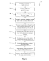
- Fig. 6 shows a flow diagram of an exemplary method 30 of manufacturing a photovoltaic device according to one embodiment of the present invention.
- a TCO layer is formed on a glass substrate at 32.
- a RTB layer is formed on the TCO layer.
- a cadmium sulfide layer is formed on the RTB layer at 36.
- a cadmium telluride layer can be formed on the cadmium sulfide layer at 38.
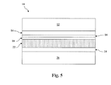
- the graded alloy telluride layer can then be formed on the cadmium telluride layer (see e.g., Figs. 1-4 ) or directly on the cadmium sulfide layer (see e.g., Fig. 5 ) at 40.
- the graded telluride layer can be annealed in the presence of cadmium chloride at 42.
- the graded alloy telluride layer can then be washed at 44 to remove any CdO formed on the surface, and doped with copper at 46.
- back contact layer(s) can be applied over the graded alloy telluride layer, and an encapsulating glass can be applied over the back contact layer at 50.
- the method may also include laser scribing to form electrically isolated photovoltaic cells in the device. These electrically isolated photovoltaic cells can then be connected in series to form a photovoltaic module. Also, electrical wires can be connected to positive and negative terminals of the photovoltaic module to provide lead wires to harness electrical current produced by the photovoltaic module.
Applications Claiming Priority (1)
| Application Number | Priority Date | Filing Date | Title |
|---|---|---|---|
| US12/639,073 US20110139247A1 (en) | 2009-12-16 | 2009-12-16 | Graded alloy telluride layer in cadmium telluride thin film photovoltaic devices and methods of manufacturing the same |
Publications (2)
| Publication Number | Publication Date |
|---|---|
| EP2337084A2 true EP2337084A2 (fr) | 2011-06-22 |
| EP2337084A3 EP2337084A3 (fr) | 2013-01-16 |
Family
ID=43881115
Family Applications (1)
| Application Number | Title | Priority Date | Filing Date |
|---|---|---|---|
| EP10194274A Withdrawn EP2337084A3 (fr) | 2009-12-16 | 2010-12-09 | Couche de tellurure d'alliage gradué dans des dispositifs photovoltaïques à film mince en tellurure de cadmium et procédés de fabrication associés |
Country Status (3)
| Country | Link |
|---|---|
| US (1) | US20110139247A1 (fr) |
| EP (1) | EP2337084A3 (fr) |
| CN (1) | CN102142475A (fr) |
Cited By (4)
| Publication number | Priority date | Publication date | Assignee | Title |
|---|---|---|---|---|
| EP2437316A3 (fr) * | 2010-09-30 | 2014-11-26 | First Solar Malaysia SDN.BHD | Dispositif photovoltaïque et procédé de fabrication |
| US9117956B2 (en) | 2012-08-31 | 2015-08-25 | First Solar, Inc. | Method of controlling the amount of Cu doping when forming a back contact of a photovoltaic cell |
| US9159864B2 (en) | 2013-07-25 | 2015-10-13 | First Solar, Inc. | Back contact paste with Te enrichment and copper doping control in thin film photovoltaic devices |
| US9306105B2 (en) | 2013-07-31 | 2016-04-05 | First Solar Malaysia Sdn. Bhd. | Finger structures protruding from absorber layer for improved solar cell back contact |
Families Citing this family (12)
| Publication number | Priority date | Publication date | Assignee | Title |
|---|---|---|---|---|
| US8252618B2 (en) * | 2009-12-15 | 2012-08-28 | Primestar Solar, Inc. | Methods of manufacturing cadmium telluride thin film photovoltaic devices |
| US20110265868A1 (en) * | 2010-04-29 | 2011-11-03 | Primestar Solar, Inc. | Cadmium sulfide layers for use in cadmium telluride based thin film photovoltaic devices and methods of their manufacture |
| CN102629630A (zh) * | 2012-04-17 | 2012-08-08 | 成都中光电阿波罗太阳能有限公司 | 背接触层及将其制作在碲化镉薄膜太阳能电池上的方法 |
| EP2973730A1 (fr) | 2013-03-15 | 2016-01-20 | First Solar, Inc | Dispositif photovoltaïque à rendement élevé utilisant du tellurure-sulfure de cadmium et procédé de fabrication |
| US9437760B2 (en) | 2013-03-15 | 2016-09-06 | First Solar, Inc. | Method of reducing semiconductor window layer loss during thin film photovoltaic device fabrication, and resulting device structure |
| WO2014210451A2 (fr) * | 2013-06-28 | 2014-12-31 | First Solar, Inc. | Procédé de fabrication d'un dispositif photovoltaïque |
| US9093599B2 (en) | 2013-07-26 | 2015-07-28 | First Solar, Inc. | Vapor deposition apparatus for continuous deposition of multiple thin film layers on a substrate |
| CN103811579B (zh) * | 2014-02-13 | 2016-09-28 | 吉林大学 | 一种柔性CdTe薄膜太阳能电池及其制备方法 |
| CN104064618A (zh) * | 2014-05-16 | 2014-09-24 | 中国科学院电工研究所 | 一种p-i-n结构CdTe电池及其制备方法 |
| DE102014225862B4 (de) * | 2014-12-15 | 2023-01-19 | China Triumph International Engineering Co., Ltd. | Verfahren zur Bildung einer Dünnschicht mit Gradient mittels Spraypyrolyse |
| CN104851931B (zh) * | 2015-04-14 | 2017-10-31 | 湖南共创光伏科技有限公司 | 具有梯度结构的碲化镉薄膜太阳能电池及其制造方法 |
| CN104810424A (zh) * | 2015-04-17 | 2015-07-29 | 四川大学 | 具有CdxTe插入层的CdTe薄膜太阳电池 |
Citations (1)
| Publication number | Priority date | Publication date | Assignee | Title |
|---|---|---|---|---|
| US20090194165A1 (en) | 2008-01-31 | 2009-08-06 | Primestar Solar, Inc. | Ultra-high current density cadmium telluride photovoltaic modules |
Family Cites Families (17)
| Publication number | Priority date | Publication date | Assignee | Title |
|---|---|---|---|---|
| US4568792A (en) * | 1984-02-02 | 1986-02-04 | Sri International | Photovoltaic cell including doped cadmium telluride, a dislocation preventing agent and improved ohmic contacts |
| US4753684A (en) * | 1986-10-31 | 1988-06-28 | The Standard Oil Company | Photovoltaic heterojunction structures |
| US4950615A (en) * | 1989-02-06 | 1990-08-21 | International Solar Electric Technology, Inc. | Method and making group IIB metal - telluride films and solar cells |
| US5248349A (en) * | 1992-05-12 | 1993-09-28 | Solar Cells, Inc. | Process for making photovoltaic devices and resultant product |
| US6265731B1 (en) * | 1992-06-03 | 2001-07-24 | Raytheon Company | Ohmic contacts for p-type wide bandgap II-VI semiconductor materials |
| US5366764A (en) * | 1992-06-15 | 1994-11-22 | Sunthankar Mandar B | Environmentally safe methods and apparatus for depositing and/or reclaiming a metal or semi-conductor material using sublimation |
| US5393675A (en) * | 1993-05-10 | 1995-02-28 | The University Of Toledo | Process for RF sputtering of cadmium telluride photovoltaic cell |
| WO1997045880A1 (fr) * | 1996-05-28 | 1997-12-04 | Matsushita Battery Industrial Co., Ltd. | Procede de formation d'un film au tellure de cadmium et d'une photopile mettant en oeuvre ce film |
| US6255708B1 (en) * | 1997-10-10 | 2001-07-03 | Rengarajan Sudharsanan | Semiconductor P-I-N detector |
| ATE374263T1 (de) * | 1999-03-29 | 2007-10-15 | Antec Solar Energy Ag | Vorrichtung und verfahren zur beschichtung von substraten durch aufdampfen mittels eines pvd- verfahrens |
| US6548751B2 (en) * | 2000-12-12 | 2003-04-15 | Solarflex Technologies, Inc. | Thin film flexible solar cell |
| US6719848B2 (en) * | 2001-08-16 | 2004-04-13 | First Solar, Llc | Chemical vapor deposition system |
| JP4269653B2 (ja) * | 2002-11-20 | 2009-05-27 | 株式会社島津製作所 | 放射線検出器の製造方法 |
| WO2009045293A2 (fr) * | 2007-09-25 | 2009-04-09 | First Solar, Inc. | Dispositifs photovoltaïques comprenant une couche interfaciale |
| WO2009117072A1 (fr) * | 2008-03-18 | 2009-09-24 | Solexant Corp. | Contact repos amélioré dans des photopiles minces |
| CA2718272A1 (fr) * | 2008-03-26 | 2009-10-01 | Puthur Paulson | Jonctions ameliorees dans des cellules solaires sur substrat |
| US8298856B2 (en) * | 2008-07-17 | 2012-10-30 | Uriel Solar, Inc. | Polycrystalline CDTE thin film semiconductor photovoltaic cell structures for use in solar electricity generation |
-
2009
- 2009-12-16 US US12/639,073 patent/US20110139247A1/en not_active Abandoned
-
2010
- 2010-12-09 EP EP10194274A patent/EP2337084A3/fr not_active Withdrawn
- 2010-12-15 CN CN2010106041401A patent/CN102142475A/zh active Pending
Patent Citations (1)
| Publication number | Priority date | Publication date | Assignee | Title |
|---|---|---|---|---|
| US20090194165A1 (en) | 2008-01-31 | 2009-08-06 | Primestar Solar, Inc. | Ultra-high current density cadmium telluride photovoltaic modules |
Cited By (4)
| Publication number | Priority date | Publication date | Assignee | Title |
|---|---|---|---|---|
| EP2437316A3 (fr) * | 2010-09-30 | 2014-11-26 | First Solar Malaysia SDN.BHD | Dispositif photovoltaïque et procédé de fabrication |
| US9117956B2 (en) | 2012-08-31 | 2015-08-25 | First Solar, Inc. | Method of controlling the amount of Cu doping when forming a back contact of a photovoltaic cell |
| US9159864B2 (en) | 2013-07-25 | 2015-10-13 | First Solar, Inc. | Back contact paste with Te enrichment and copper doping control in thin film photovoltaic devices |
| US9306105B2 (en) | 2013-07-31 | 2016-04-05 | First Solar Malaysia Sdn. Bhd. | Finger structures protruding from absorber layer for improved solar cell back contact |
Also Published As
| Publication number | Publication date |
|---|---|
| EP2337084A3 (fr) | 2013-01-16 |
| CN102142475A (zh) | 2011-08-03 |
| US20110139247A1 (en) | 2011-06-16 |
Similar Documents
| Publication | Publication Date | Title |
|---|---|---|
| EP2337084A2 (fr) | Couche de tellurure d'alliage gradué dans des dispositifs photovoltaïques à film mince en tellurure de cadmium et procédés de fabrication associés | |
| US8143515B2 (en) | Cadmium telluride thin film photovoltaic devices and methods of manufacturing the same | |
| US8252618B2 (en) | Methods of manufacturing cadmium telluride thin film photovoltaic devices | |
| US8043955B1 (en) | Methods of forming a conductive transparent oxide film layer for use in a cadmium telluride based thin film photovoltaic device | |
| US7943415B1 (en) | Methods of sputtering cadmium sulfide layers for use in cadmium telluride based thin film photovoltaic devices | |
| US20120061235A1 (en) | Mixed sputtering target of cadmium sulfide and cadmium telluride and methods of their use | |
| EP2448004A1 (fr) | Mélange de couches de sulfure de cadmium et couche de tellurure de cadmium pour dispositifs photovoltaïques à couche mince et leurs procédés de fabrication | |
| EP2383363B1 (fr) | Couches de sulfure de cadmium pour dispositifs photovoltaïques à couche mince en tellurure de cadmium et leur procédé de fabrication | |
| US8247683B2 (en) | Thin film interlayer in cadmium telluride thin film photovoltaic devices and methods of manufacturing the same | |
| EP2403000A2 (fr) | Quadrillages métalliques en tant que contacts frontaux d'un dispositif photovoltaïque à film mince à base de tellurure de cadmium | |
| US8053350B2 (en) | Methods of forming a conductive transparent oxide film layer for use in a cadmium telluride based thin film photovoltaic device | |
| EP2530726A2 (fr) | Empilement de type n multicouche pour dispositifs photovoltaïques à couche mince à base de tellurure de cadmium et procédés de fabrication | |
| EP2371990B1 (fr) | Procédés de formation d'une couche de film d'oxyde conducteur transparent pour une utilisation dans un dispositif photovoltaïque à couche mince à base de tellurure de cadmium | |
| EP2383792A2 (fr) | Couches de sulfure de cadmium à utiliser dans les dispositifs photovoltaïques à couche mince en tellurure de cadmium et leurs procédés de fabrication | |
| EP2402479B1 (fr) | Procédé de pulvérisation de couche mince transparente resisive pour dispositifs photovoltaïques en tellurure de cadmium | |
| US8241930B2 (en) | Methods of forming a window layer in a cadmium telluride based thin film photovoltaic device | |
| US20130019948A1 (en) | Stabilized back contact for photovoltaic devices and methods of their manufacture | |
| EP2530727A2 (fr) | Empilement de type n multicouche pour dispositifs photovoltaïques à couche mince à base de tellurure de cadmium et procédés de fabrication | |
| US20120024692A1 (en) | Mixed sputtering targets and their use in cadmium sulfide layers of cadmium telluride vased thin film photovoltaic devices | |
| US20130133731A1 (en) | Cadmium doped tin oxide buffer layer for thin film photovoltaic devices and their methods of manufacture | |
| US20130134037A1 (en) | Mixed targets for forming a cadmium doped tin oxide buffer layer in a thin film photovoltaic devices |
Legal Events
| Date | Code | Title | Description |
|---|---|---|---|
| PUAI | Public reference made under article 153(3) epc to a published international application that has entered the european phase |
Free format text: ORIGINAL CODE: 0009012 |
|
| AK | Designated contracting states |
Kind code of ref document: A2 Designated state(s): AL AT BE BG CH CY CZ DE DK EE ES FI FR GB GR HR HU IE IS IT LI LT LU LV MC MK MT NL NO PL PT RO RS SE SI SK SM TR |
|
| AX | Request for extension of the european patent |
Extension state: BA ME |
|
| PUAL | Search report despatched |
Free format text: ORIGINAL CODE: 0009013 |
|
| AK | Designated contracting states |
Kind code of ref document: A3 Designated state(s): AL AT BE BG CH CY CZ DE DK EE ES FI FR GB GR HR HU IE IS IT LI LT LU LV MC MK MT NL NO PL PT RO RS SE SI SK SM TR |
|
| AX | Request for extension of the european patent |
Extension state: BA ME |
|
| RIC1 | Information provided on ipc code assigned before grant |
Ipc: H01L 31/18 20060101ALI20121213BHEP Ipc: H01L 31/0296 20060101AFI20121213BHEP Ipc: C23C 14/06 20060101ALI20121213BHEP Ipc: H01L 31/073 20120101ALI20121213BHEP Ipc: C23C 14/34 20060101ALI20121213BHEP |
|
| STAA | Information on the status of an ep patent application or granted ep patent |
Free format text: STATUS: THE APPLICATION IS DEEMED TO BE WITHDRAWN |
|
| 18D | Application deemed to be withdrawn |
Effective date: 20130702 |