EP2527145B1 - System and method for manufacturing liquid crystal display element using a lamination process - Google Patents
System and method for manufacturing liquid crystal display element using a lamination process Download PDFInfo
- Publication number
- EP2527145B1 EP2527145B1 EP12181127.7A EP12181127A EP2527145B1 EP 2527145 B1 EP2527145 B1 EP 2527145B1 EP 12181127 A EP12181127 A EP 12181127A EP 2527145 B1 EP2527145 B1 EP 2527145B1
- Authority
- EP
- European Patent Office
- Prior art keywords
- liquid crystal
- crystal panel
- optical functional
- film
- panel
- Prior art date
- Legal status (The legal status is an assumption and is not a legal conclusion. Google has not performed a legal analysis and makes no representation as to the accuracy of the status listed.)
- Not-in-force
Links
Images


Classifications
-
- G—PHYSICS
- G02—OPTICS
- G02F—OPTICAL DEVICES OR ARRANGEMENTS FOR THE CONTROL OF LIGHT BY MODIFICATION OF THE OPTICAL PROPERTIES OF THE MEDIA OF THE ELEMENTS INVOLVED THEREIN; NON-LINEAR OPTICS; FREQUENCY-CHANGING OF LIGHT; OPTICAL LOGIC ELEMENTS; OPTICAL ANALOGUE/DIGITAL CONVERTERS
- G02F1/00—Devices or arrangements for the control of the intensity, colour, phase, polarisation or direction of light arriving from an independent light source, e.g. switching, gating or modulating; Non-linear optics
- G02F1/01—Devices or arrangements for the control of the intensity, colour, phase, polarisation or direction of light arriving from an independent light source, e.g. switching, gating or modulating; Non-linear optics for the control of the intensity, phase, polarisation or colour
- G02F1/13—Devices or arrangements for the control of the intensity, colour, phase, polarisation or direction of light arriving from an independent light source, e.g. switching, gating or modulating; Non-linear optics for the control of the intensity, phase, polarisation or colour based on liquid crystals, e.g. single liquid crystal display cells
- G02F1/133—Constructional arrangements; Operation of liquid crystal cells; Circuit arrangements
- G02F1/1333—Constructional arrangements; Manufacturing methods
- G02F1/1335—Structural association of cells with optical devices, e.g. polarisers or reflectors
-
- B—PERFORMING OPERATIONS; TRANSPORTING
- B29—WORKING OF PLASTICS; WORKING OF SUBSTANCES IN A PLASTIC STATE IN GENERAL
- B29D—PRODUCING PARTICULAR ARTICLES FROM PLASTICS OR FROM SUBSTANCES IN A PLASTIC STATE
- B29D11/00—Producing optical elements, e.g. lenses or prisms
- B29D11/0073—Optical laminates
-
- B—PERFORMING OPERATIONS; TRANSPORTING
- B32—LAYERED PRODUCTS
- B32B—LAYERED PRODUCTS, i.e. PRODUCTS BUILT-UP OF STRATA OF FLAT OR NON-FLAT, e.g. CELLULAR OR HONEYCOMB, FORM
- B32B38/00—Ancillary operations in connection with laminating processes
- B32B38/18—Handling of layers or the laminate
-
- G—PHYSICS
- G02—OPTICS
- G02B—OPTICAL ELEMENTS, SYSTEMS OR APPARATUS
- G02B5/00—Optical elements other than lenses
- G02B5/30—Polarising elements
-
- G—PHYSICS
- G02—OPTICS
- G02F—OPTICAL DEVICES OR ARRANGEMENTS FOR THE CONTROL OF LIGHT BY MODIFICATION OF THE OPTICAL PROPERTIES OF THE MEDIA OF THE ELEMENTS INVOLVED THEREIN; NON-LINEAR OPTICS; FREQUENCY-CHANGING OF LIGHT; OPTICAL LOGIC ELEMENTS; OPTICAL ANALOGUE/DIGITAL CONVERTERS
- G02F1/00—Devices or arrangements for the control of the intensity, colour, phase, polarisation or direction of light arriving from an independent light source, e.g. switching, gating or modulating; Non-linear optics
- G02F1/01—Devices or arrangements for the control of the intensity, colour, phase, polarisation or direction of light arriving from an independent light source, e.g. switching, gating or modulating; Non-linear optics for the control of the intensity, phase, polarisation or colour
- G02F1/13—Devices or arrangements for the control of the intensity, colour, phase, polarisation or direction of light arriving from an independent light source, e.g. switching, gating or modulating; Non-linear optics for the control of the intensity, phase, polarisation or colour based on liquid crystals, e.g. single liquid crystal display cells
- G02F1/1303—Apparatus specially adapted to the manufacture of LCDs
-
- B—PERFORMING OPERATIONS; TRANSPORTING
- B32—LAYERED PRODUCTS
- B32B—LAYERED PRODUCTS, i.e. PRODUCTS BUILT-UP OF STRATA OF FLAT OR NON-FLAT, e.g. CELLULAR OR HONEYCOMB, FORM
- B32B2457/00—Electrical equipment
- B32B2457/20—Displays, e.g. liquid crystal displays, plasma displays
- B32B2457/202—LCD, i.e. liquid crystal displays
-
- G—PHYSICS
- G02—OPTICS
- G02F—OPTICAL DEVICES OR ARRANGEMENTS FOR THE CONTROL OF LIGHT BY MODIFICATION OF THE OPTICAL PROPERTIES OF THE MEDIA OF THE ELEMENTS INVOLVED THEREIN; NON-LINEAR OPTICS; FREQUENCY-CHANGING OF LIGHT; OPTICAL LOGIC ELEMENTS; OPTICAL ANALOGUE/DIGITAL CONVERTERS
- G02F1/00—Devices or arrangements for the control of the intensity, colour, phase, polarisation or direction of light arriving from an independent light source, e.g. switching, gating or modulating; Non-linear optics
- G02F1/01—Devices or arrangements for the control of the intensity, colour, phase, polarisation or direction of light arriving from an independent light source, e.g. switching, gating or modulating; Non-linear optics for the control of the intensity, phase, polarisation or colour
- G02F1/13—Devices or arrangements for the control of the intensity, colour, phase, polarisation or direction of light arriving from an independent light source, e.g. switching, gating or modulating; Non-linear optics for the control of the intensity, phase, polarisation or colour based on liquid crystals, e.g. single liquid crystal display cells
- G02F1/133—Constructional arrangements; Operation of liquid crystal cells; Circuit arrangements
- G02F1/1333—Constructional arrangements; Manufacturing methods
- G02F1/1335—Structural association of cells with optical devices, e.g. polarisers or reflectors
- G02F1/133528—Polarisers
Definitions
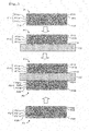
- the laminated structure of the second optical film laminate F2 is the same as, but not limited to, that of the first optical film laminate F1.
- the second optical film laminate F2 has a structure in which a second optical functional film F21, a second carrier film F22, and a surface protecting film F23 are stacked.
- the second optical functional film F21 includes a polarizing film.
- the second optical functional film F21 includes a second polarizer F21a, a third film F21b bonded to one side thereof with an adhesive layer (not shown) interposed therebetween, and a fourth film F21c bonded to the other side thereof with an adhesive layer (not shown) interposed therebetween.
- the second polarizer F21a is typically formed by drying a polyvinyl alcohol (PVA) film. It will be understood that the second polarizer F21a may be formed using any other film than the polyvinyl alcohol film.
- PVA polyvinyl alcohol
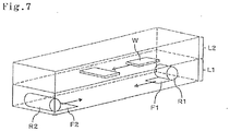
- the liquid crystal panel W used was a 40-inch panel, which is a typical large panel (such as a panel of 32 inches or more).
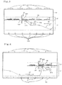
- the liquid crystal panel W has to be horizontally rotated so that the optical functional films F11 and F21 can be bonded in a crossed nicols relationship. In the configuration shown in Fig. 8B(a) , however, there is no need to rotate the liquid crystal panel W horizontally.
- Comparative Example 3 an L-shaped manufacturing line as shown in Fig. 8B(a) was used, and neither turning over the liquid crystal panel W nor rotating it horizontally was performed, when one of the optical functional films F11 and F21 was bonded to the liquid crystal panel W from above and the other was bonded thereto from below.
- the manufacturing line had a width W1 of 12.5 m, a length W2 of 14.0 m, a bonding region installation area of 175.0 m 2 , and a bonding region line length of 24.5 m.
- the optical functional films F11 and F21 are bonded in different directions (from above or below) to the liquid crystal panel W, and therefore, an extra space is necessary for running of the optical functional films F11 and F21.
- W2 is 1.5 m longer than that in Comparative Example 1.
- the rate of liquid crystal display elements determined to be defective due to the occurrence of foreign bodies was 7.6% per 100 liquid crystal display elements manufactured using this manufacturing line, and the rate of occurrence of foreign bodies was found to be relatively high.
Landscapes
- Physics & Mathematics (AREA)
- Nonlinear Science (AREA)
- Engineering & Computer Science (AREA)
- Optics & Photonics (AREA)
- General Physics & Mathematics (AREA)
- Crystallography & Structural Chemistry (AREA)
- Chemical & Material Sciences (AREA)
- Manufacturing & Machinery (AREA)
- Health & Medical Sciences (AREA)
- Mechanical Engineering (AREA)
- Ophthalmology & Optometry (AREA)
- Liquid Crystal (AREA)
- Mathematical Physics (AREA)
- Polarising Elements (AREA)
- Investigating Materials By The Use Of Optical Means Adapted For Particular Applications (AREA)
Applications Claiming Priority (3)
| Application Number | Priority Date | Filing Date | Title |
|---|---|---|---|
| JP2010209729 | 2010-09-17 | ||
| JP2010251958A JP4723044B1 (ja) | 2010-09-17 | 2010-11-10 | 液晶表示素子の製造システム及び製造方法 |
| EP11153676.9A EP2431309B1 (en) | 2010-09-17 | 2011-02-08 | System and method for manufacturing liquid crystal display element |
Related Parent Applications (3)
| Application Number | Title | Priority Date | Filing Date |
|---|---|---|---|
| EP11153676.9A Division-Into EP2431309B1 (en) | 2010-09-17 | 2011-02-08 | System and method for manufacturing liquid crystal display element |
| EP11153676.9A Division EP2431309B1 (en) | 2010-09-17 | 2011-02-08 | System and method for manufacturing liquid crystal display element |
| EP11153676.9 Division | 2011-02-08 |
Publications (2)
| Publication Number | Publication Date |
|---|---|
| EP2527145A1 EP2527145A1 (en) | 2012-11-28 |
| EP2527145B1 true EP2527145B1 (en) | 2018-01-03 |
Family
ID=44350520
Family Applications (4)
| Application Number | Title | Priority Date | Filing Date |
|---|---|---|---|
| EP12181127.7A Not-in-force EP2527145B1 (en) | 2010-09-17 | 2011-02-08 | System and method for manufacturing liquid crystal display element using a lamination process |
| EP12181129A Withdrawn EP2527146A1 (en) | 2010-09-17 | 2011-02-08 | System and method for manufacturing a liquid crystal display element using a lamination process |
| EP11153676.9A Active EP2431309B1 (en) | 2010-09-17 | 2011-02-08 | System and method for manufacturing liquid crystal display element |
| EP12181128A Withdrawn EP2527276A1 (en) | 2010-09-17 | 2011-02-08 | System and method for manufacturing a liquid crystal display element using a lamination process |
Family Applications After (3)
| Application Number | Title | Priority Date | Filing Date |
|---|---|---|---|
| EP12181129A Withdrawn EP2527146A1 (en) | 2010-09-17 | 2011-02-08 | System and method for manufacturing a liquid crystal display element using a lamination process |
| EP11153676.9A Active EP2431309B1 (en) | 2010-09-17 | 2011-02-08 | System and method for manufacturing liquid crystal display element |
| EP12181128A Withdrawn EP2527276A1 (en) | 2010-09-17 | 2011-02-08 | System and method for manufacturing a liquid crystal display element using a lamination process |
Country Status (7)
| Country | Link |
|---|---|
| US (1) | US8172631B2 (enExample) |
| EP (4) | EP2527145B1 (enExample) |
| JP (1) | JP4723044B1 (enExample) |
| KR (1) | KR101051870B1 (enExample) |
| CN (2) | CN201984260U (enExample) |
| PL (1) | PL2431309T3 (enExample) |
| TW (1) | TW201213929A (enExample) |
Families Citing this family (16)
| Publication number | Priority date | Publication date | Assignee | Title |
|---|---|---|---|---|
| JP4723044B1 (ja) * | 2010-09-17 | 2011-07-13 | 日東電工株式会社 | 液晶表示素子の製造システム及び製造方法 |
| JP4676026B1 (ja) | 2010-09-17 | 2011-04-27 | 日東電工株式会社 | 液晶表示素子の製造システム及び製造方法 |
| JP4733227B1 (ja) * | 2010-09-30 | 2011-07-27 | 日東電工株式会社 | 液晶表示素子の製造システム及び製造方法 |
| JP5197708B2 (ja) * | 2010-10-13 | 2013-05-15 | 日東電工株式会社 | 液晶表示素子の連続製造方法および液晶表示素子の連続製造システム |
| JP4729647B1 (ja) * | 2010-11-02 | 2011-07-20 | 日東電工株式会社 | 液晶表示素子の製造システム |
| CN103465017B (zh) * | 2012-06-08 | 2016-05-04 | 京东方科技集团股份有限公司 | 背光源膜材组立设备 |
| KR101932562B1 (ko) * | 2012-09-18 | 2018-12-28 | 삼성디스플레이 주식회사 | 필름 부착장치 및 그것을 이용한 필름 부착방법 |
| US9498943B2 (en) * | 2014-01-08 | 2016-11-22 | Lg Chem, Ltd. | System for laminating optical film and method for manufacturing display unit using the same |
| US9914289B2 (en) | 2014-01-08 | 2018-03-13 | Lg Chem, Ltd. | System for laminating optical film and method for manufacturing display unit using the same |
| US9682543B2 (en) * | 2014-01-08 | 2017-06-20 | Lg Chem, Ltd. | System for laminating optical film and method for manufacturing display unit using the same |
| KR101495763B1 (ko) * | 2014-02-28 | 2015-02-25 | 주식회사 엘지화학 | 광학 필름 라미네이팅 시스템 및 이를 이용한 디스플레이 유닛 제조방법 |
| US9498942B2 (en) * | 2014-02-28 | 2016-11-22 | Lg Chem, Ltd. | System for laminating optical film and method for manufacturing display unit using the same |
| JP6280966B1 (ja) | 2016-10-04 | 2018-02-14 | 日東電工株式会社 | 省スペース型の光学機能フィルム貼合装置 |
| JP7012572B2 (ja) * | 2017-04-26 | 2022-01-28 | 住友化学株式会社 | 搬送装置および積層体の製造方法 |
| CN108642215A (zh) * | 2018-05-12 | 2018-10-12 | 安徽工程大学 | 一种皮具生产用烘箱 |
| KR102224043B1 (ko) | 2018-07-09 | 2021-03-08 | 주식회사 엘지화학 | 광학 표시소자 제조 시스템 및 방법 |
Family Cites Families (15)
| Publication number | Priority date | Publication date | Assignee | Title |
|---|---|---|---|---|
| JP2823970B2 (ja) * | 1991-04-05 | 1998-11-11 | 浜松ホトニクス株式会社 | 近接場走査光学顕微鏡 |
| JPH10264071A (ja) * | 1997-03-24 | 1998-10-06 | Hitachi Ltd | 基板搬送装置 |
| JP2005037417A (ja) * | 2002-06-28 | 2005-02-10 | Fuji Photo Film Co Ltd | 偏光板貼合方法及び装置 |
| KR20040002796A (ko) | 2002-06-28 | 2004-01-07 | 후지 샤신 필름 가부시기가이샤 | 편광판 점착방법 및 그 장치 |
| JP2004144908A (ja) * | 2002-10-23 | 2004-05-20 | Yodogawa Medekku Kk | 偏光板貼付装置 |
| JP3637350B2 (ja) * | 2004-01-19 | 2005-04-13 | 株式会社東芝 | 粘着性テ−プ片の貼着装置 |
| WO2009054519A1 (ja) * | 2007-10-25 | 2009-04-30 | Sumitomo Chemical Company, Limited | 光学表示パネルの製造方法 |
| JP4307510B1 (ja) | 2007-12-27 | 2009-08-05 | 日東電工株式会社 | 光学表示装置の製造システム及び製造方法 |
| US8366858B2 (en) | 2007-12-27 | 2013-02-05 | Nitto Denko Corporation | Manufacturing system and manufacturing method for optical display device |
| JP2009205138A (ja) * | 2008-01-28 | 2009-09-10 | Nitto Denko Corp | 光学表示ユニットの製造方法および製造システム |
| JP4674261B2 (ja) * | 2008-04-15 | 2011-04-20 | 日東電工株式会社 | 光学表示装置の製造方法及び製造システム |
| JP4406043B2 (ja) | 2008-04-16 | 2010-01-27 | 日東電工株式会社 | ロール原反セット、及びロール原反の製造方法 |
| JP5311277B2 (ja) | 2008-07-29 | 2013-10-09 | 日本電気硝子株式会社 | 板状ワークの移送設備および移送方法 |
| JP4628488B1 (ja) * | 2009-05-15 | 2011-02-09 | 日東電工株式会社 | 光学表示装置の製造システム及び製造方法 |
| JP4723044B1 (ja) * | 2010-09-17 | 2011-07-13 | 日東電工株式会社 | 液晶表示素子の製造システム及び製造方法 |
-
2010
- 2010-11-10 JP JP2010251958A patent/JP4723044B1/ja active Active
- 2010-11-22 TW TW099140220A patent/TW201213929A/zh unknown
-
2011
- 2011-01-19 KR KR1020110005537A patent/KR101051870B1/ko active Active
- 2011-02-04 US US13/021,294 patent/US8172631B2/en active Active
- 2011-02-08 EP EP12181127.7A patent/EP2527145B1/en not_active Not-in-force
- 2011-02-08 PL PL11153676T patent/PL2431309T3/pl unknown
- 2011-02-08 EP EP12181129A patent/EP2527146A1/en not_active Withdrawn
- 2011-02-08 EP EP11153676.9A patent/EP2431309B1/en active Active
- 2011-02-08 EP EP12181128A patent/EP2527276A1/en not_active Withdrawn
- 2011-03-21 CN CN2011200763739U patent/CN201984260U/zh not_active Expired - Lifetime
- 2011-03-21 CN CN201110068158.9A patent/CN102411226B/zh active Active
Non-Patent Citations (1)
| Title |
|---|
| None * |
Also Published As
| Publication number | Publication date |
|---|---|
| EP2431309B1 (en) | 2014-12-03 |
| EP2527276A1 (en) | 2012-11-28 |
| KR101051870B1 (ko) | 2011-07-25 |
| US20120071057A1 (en) | 2012-03-22 |
| TWI356927B (enExample) | 2012-01-21 |
| JP4723044B1 (ja) | 2011-07-13 |
| EP2527145A1 (en) | 2012-11-28 |
| JP2012083690A (ja) | 2012-04-26 |
| CN201984260U (zh) | 2011-09-21 |
| TW201213929A (en) | 2012-04-01 |
| EP2431309A1 (en) | 2012-03-21 |
| CN102411226A (zh) | 2012-04-11 |
| EP2527146A1 (en) | 2012-11-28 |
| CN102411226B (zh) | 2015-07-22 |
| PL2431309T3 (pl) | 2015-05-29 |
| US8172631B2 (en) | 2012-05-08 |
Similar Documents
| Publication | Publication Date | Title |
|---|---|---|
| EP2527145B1 (en) | System and method for manufacturing liquid crystal display element using a lamination process | |
| EP2431799B1 (en) | System and method for manufacturing liquid crystal display element | |
| JP4669070B2 (ja) | 光学表示装置の製造システム及び製造方法 | |
| TWI457636B (zh) | Manufacturing system and manufacturing method of optical display device, and roll-type material group and manufacturing method thereof | |
| US8893759B2 (en) | System for manufacturing liquid crystal display device | |
| TWI391726B (zh) | Optical display device manufacturing system and optical display device manufacturing method | |
| EP2447062B1 (en) | System for manufacturing liquid crystal display device |
Legal Events
| Date | Code | Title | Description |
|---|---|---|---|
| PUAI | Public reference made under article 153(3) epc to a published international application that has entered the european phase |
Free format text: ORIGINAL CODE: 0009012 |
|
| AC | Divisional application: reference to earlier application |
Ref document number: 2431309 Country of ref document: EP Kind code of ref document: P |
|
| AK | Designated contracting states |
Kind code of ref document: A1 Designated state(s): AL AT BE BG CH CY CZ DE DK EE ES FI FR GB GR HR HU IE IS IT LI LT LU LV MC MK MT NL NO PL PT RO RS SE SI SK SM TR |
|
| AX | Request for extension of the european patent |
Extension state: BA ME |
|
| 17P | Request for examination filed |
Effective date: 20130523 |
|
| RBV | Designated contracting states (corrected) |
Designated state(s): AL AT BE BG CH CY CZ DE DK EE ES FI FR GB GR HR HU IE IS IT LI LT LU LV MC MK MT NL NO PL PT RO RS SE SI SK SM TR |
|
| 17Q | First examination report despatched |
Effective date: 20131018 |
|
| RIC1 | Information provided on ipc code assigned before grant |
Ipc: B29D 11/00 20060101ALI20170412BHEP Ipc: B32B 38/18 20060101AFI20170412BHEP Ipc: B65G 49/06 20060101ALI20170412BHEP Ipc: G02F 1/1335 20060101ALN20170412BHEP Ipc: G02B 5/30 20060101ALI20170412BHEP Ipc: B65H 9/00 20060101ALI20170412BHEP Ipc: G02F 1/13 20060101ALN20170412BHEP |
|
| GRAP | Despatch of communication of intention to grant a patent |
Free format text: ORIGINAL CODE: EPIDOSNIGR1 |
|
| INTG | Intention to grant announced |
Effective date: 20170523 |
|
| GRAJ | Information related to disapproval of communication of intention to grant by the applicant or resumption of examination proceedings by the epo deleted |
Free format text: ORIGINAL CODE: EPIDOSDIGR1 |
|
| INTC | Intention to grant announced (deleted) | ||
| RIC1 | Information provided on ipc code assigned before grant |
Ipc: B32B 38/18 20060101AFI20170802BHEP Ipc: G02B 5/30 20060101ALI20170802BHEP Ipc: B65G 49/06 20060101ALI20170802BHEP Ipc: B29D 11/00 20060101ALI20170802BHEP Ipc: B65H 9/00 20060101ALI20170802BHEP Ipc: G02F 1/13 20060101ALN20170802BHEP Ipc: G02F 1/1335 20060101ALN20170802BHEP |
|
| RIC1 | Information provided on ipc code assigned before grant |
Ipc: B29D 11/00 20060101ALI20170809BHEP Ipc: B65G 49/06 20060101ALI20170809BHEP Ipc: B65H 9/00 20060101ALI20170809BHEP Ipc: B32B 38/18 20060101AFI20170809BHEP Ipc: G02F 1/1335 20060101ALN20170809BHEP Ipc: G02B 5/30 20060101ALI20170809BHEP Ipc: G02F 1/13 20060101ALN20170809BHEP |
|
| GRAP | Despatch of communication of intention to grant a patent |
Free format text: ORIGINAL CODE: EPIDOSNIGR1 |
|
| INTG | Intention to grant announced |
Effective date: 20170921 |
|
| GRAS | Grant fee paid |
Free format text: ORIGINAL CODE: EPIDOSNIGR3 |
|
| GRAA | (expected) grant |
Free format text: ORIGINAL CODE: 0009210 |
|
| AC | Divisional application: reference to earlier application |
Ref document number: 2431309 Country of ref document: EP Kind code of ref document: P |
|
| AK | Designated contracting states |
Kind code of ref document: B1 Designated state(s): AL AT BE BG CH CY CZ DE DK EE ES FI FR GB GR HR HU IE IS IT LI LT LU LV MC MK MT NL NO PL PT RO RS SE SI SK SM TR |
|
| REG | Reference to a national code |
Ref country code: GB Ref legal event code: FG4D |
|
| REG | Reference to a national code |
Ref country code: CH Ref legal event code: EP Ref country code: AT Ref legal event code: REF Ref document number: 959845 Country of ref document: AT Kind code of ref document: T Effective date: 20180115 |
|
| REG | Reference to a national code |
Ref country code: IE Ref legal event code: FG4D |
|
| REG | Reference to a national code |
Ref country code: DE Ref legal event code: R096 Ref document number: 602011044838 Country of ref document: DE |
|
| REG | Reference to a national code |
Ref country code: NL Ref legal event code: MP Effective date: 20180103 |
|
| REG | Reference to a national code |
Ref country code: LT Ref legal event code: MG4D |
|
| REG | Reference to a national code |
Ref country code: AT Ref legal event code: MK05 Ref document number: 959845 Country of ref document: AT Kind code of ref document: T Effective date: 20180103 |
|
| PG25 | Lapsed in a contracting state [announced via postgrant information from national office to epo] |
Ref country code: NL Free format text: LAPSE BECAUSE OF FAILURE TO SUBMIT A TRANSLATION OF THE DESCRIPTION OR TO PAY THE FEE WITHIN THE PRESCRIBED TIME-LIMIT Effective date: 20180103 |
|
| PG25 | Lapsed in a contracting state [announced via postgrant information from national office to epo] |
Ref country code: ES Free format text: LAPSE BECAUSE OF FAILURE TO SUBMIT A TRANSLATION OF THE DESCRIPTION OR TO PAY THE FEE WITHIN THE PRESCRIBED TIME-LIMIT Effective date: 20180103 Ref country code: CY Free format text: LAPSE BECAUSE OF FAILURE TO SUBMIT A TRANSLATION OF THE DESCRIPTION OR TO PAY THE FEE WITHIN THE PRESCRIBED TIME-LIMIT Effective date: 20180103 Ref country code: HR Free format text: LAPSE BECAUSE OF FAILURE TO SUBMIT A TRANSLATION OF THE DESCRIPTION OR TO PAY THE FEE WITHIN THE PRESCRIBED TIME-LIMIT Effective date: 20180103 Ref country code: LT Free format text: LAPSE BECAUSE OF FAILURE TO SUBMIT A TRANSLATION OF THE DESCRIPTION OR TO PAY THE FEE WITHIN THE PRESCRIBED TIME-LIMIT Effective date: 20180103 Ref country code: NO Free format text: LAPSE BECAUSE OF FAILURE TO SUBMIT A TRANSLATION OF THE DESCRIPTION OR TO PAY THE FEE WITHIN THE PRESCRIBED TIME-LIMIT Effective date: 20180403 Ref country code: FI Free format text: LAPSE BECAUSE OF FAILURE TO SUBMIT A TRANSLATION OF THE DESCRIPTION OR TO PAY THE FEE WITHIN THE PRESCRIBED TIME-LIMIT Effective date: 20180103 |
|
| PG25 | Lapsed in a contracting state [announced via postgrant information from national office to epo] |
Ref country code: IS Free format text: LAPSE BECAUSE OF FAILURE TO SUBMIT A TRANSLATION OF THE DESCRIPTION OR TO PAY THE FEE WITHIN THE PRESCRIBED TIME-LIMIT Effective date: 20180503 Ref country code: BG Free format text: LAPSE BECAUSE OF FAILURE TO SUBMIT A TRANSLATION OF THE DESCRIPTION OR TO PAY THE FEE WITHIN THE PRESCRIBED TIME-LIMIT Effective date: 20180403 Ref country code: SE Free format text: LAPSE BECAUSE OF FAILURE TO SUBMIT A TRANSLATION OF THE DESCRIPTION OR TO PAY THE FEE WITHIN THE PRESCRIBED TIME-LIMIT Effective date: 20180103 Ref country code: AT Free format text: LAPSE BECAUSE OF FAILURE TO SUBMIT A TRANSLATION OF THE DESCRIPTION OR TO PAY THE FEE WITHIN THE PRESCRIBED TIME-LIMIT Effective date: 20180103 Ref country code: LV Free format text: LAPSE BECAUSE OF FAILURE TO SUBMIT A TRANSLATION OF THE DESCRIPTION OR TO PAY THE FEE WITHIN THE PRESCRIBED TIME-LIMIT Effective date: 20180103 Ref country code: RS Free format text: LAPSE BECAUSE OF FAILURE TO SUBMIT A TRANSLATION OF THE DESCRIPTION OR TO PAY THE FEE WITHIN THE PRESCRIBED TIME-LIMIT Effective date: 20180103 Ref country code: PL Free format text: LAPSE BECAUSE OF FAILURE TO SUBMIT A TRANSLATION OF THE DESCRIPTION OR TO PAY THE FEE WITHIN THE PRESCRIBED TIME-LIMIT Effective date: 20180103 Ref country code: GR Free format text: LAPSE BECAUSE OF FAILURE TO SUBMIT A TRANSLATION OF THE DESCRIPTION OR TO PAY THE FEE WITHIN THE PRESCRIBED TIME-LIMIT Effective date: 20180404 |
|
| REG | Reference to a national code |
Ref country code: CH Ref legal event code: PL |
|
| REG | Reference to a national code |
Ref country code: DE Ref legal event code: R097 Ref document number: 602011044838 Country of ref document: DE |
|
| PG25 | Lapsed in a contracting state [announced via postgrant information from national office to epo] |
Ref country code: EE Free format text: LAPSE BECAUSE OF FAILURE TO SUBMIT A TRANSLATION OF THE DESCRIPTION OR TO PAY THE FEE WITHIN THE PRESCRIBED TIME-LIMIT Effective date: 20180103 Ref country code: RO Free format text: LAPSE BECAUSE OF FAILURE TO SUBMIT A TRANSLATION OF THE DESCRIPTION OR TO PAY THE FEE WITHIN THE PRESCRIBED TIME-LIMIT Effective date: 20180103 Ref country code: AL Free format text: LAPSE BECAUSE OF FAILURE TO SUBMIT A TRANSLATION OF THE DESCRIPTION OR TO PAY THE FEE WITHIN THE PRESCRIBED TIME-LIMIT Effective date: 20180103 Ref country code: MC Free format text: LAPSE BECAUSE OF FAILURE TO SUBMIT A TRANSLATION OF THE DESCRIPTION OR TO PAY THE FEE WITHIN THE PRESCRIBED TIME-LIMIT Effective date: 20180103 Ref country code: IT Free format text: LAPSE BECAUSE OF FAILURE TO SUBMIT A TRANSLATION OF THE DESCRIPTION OR TO PAY THE FEE WITHIN THE PRESCRIBED TIME-LIMIT Effective date: 20180103 |
|
| PLBE | No opposition filed within time limit |
Free format text: ORIGINAL CODE: 0009261 |
|
| STAA | Information on the status of an ep patent application or granted ep patent |
Free format text: STATUS: NO OPPOSITION FILED WITHIN TIME LIMIT |
|
| REG | Reference to a national code |
Ref country code: IE Ref legal event code: MM4A |
|
| REG | Reference to a national code |
Ref country code: BE Ref legal event code: MM Effective date: 20180228 |
|
| PG25 | Lapsed in a contracting state [announced via postgrant information from national office to epo] |
Ref country code: LU Free format text: LAPSE BECAUSE OF NON-PAYMENT OF DUE FEES Effective date: 20180208 Ref country code: LI Free format text: LAPSE BECAUSE OF NON-PAYMENT OF DUE FEES Effective date: 20180228 Ref country code: SM Free format text: LAPSE BECAUSE OF FAILURE TO SUBMIT A TRANSLATION OF THE DESCRIPTION OR TO PAY THE FEE WITHIN THE PRESCRIBED TIME-LIMIT Effective date: 20180103 Ref country code: CH Free format text: LAPSE BECAUSE OF NON-PAYMENT OF DUE FEES Effective date: 20180228 Ref country code: DK Free format text: LAPSE BECAUSE OF FAILURE TO SUBMIT A TRANSLATION OF THE DESCRIPTION OR TO PAY THE FEE WITHIN THE PRESCRIBED TIME-LIMIT Effective date: 20180103 Ref country code: SK Free format text: LAPSE BECAUSE OF FAILURE TO SUBMIT A TRANSLATION OF THE DESCRIPTION OR TO PAY THE FEE WITHIN THE PRESCRIBED TIME-LIMIT Effective date: 20180103 Ref country code: CZ Free format text: LAPSE BECAUSE OF FAILURE TO SUBMIT A TRANSLATION OF THE DESCRIPTION OR TO PAY THE FEE WITHIN THE PRESCRIBED TIME-LIMIT Effective date: 20180103 |
|
| REG | Reference to a national code |
Ref country code: FR Ref legal event code: ST Effective date: 20181031 |
|
| 26N | No opposition filed |
Effective date: 20181005 |
|
| GBPC | Gb: european patent ceased through non-payment of renewal fee |
Effective date: 20180403 |
|
| PG25 | Lapsed in a contracting state [announced via postgrant information from national office to epo] |
Ref country code: IE Free format text: LAPSE BECAUSE OF NON-PAYMENT OF DUE FEES Effective date: 20180208 |
|
| PG25 | Lapsed in a contracting state [announced via postgrant information from national office to epo] |
Ref country code: FR Free format text: LAPSE BECAUSE OF NON-PAYMENT OF DUE FEES Effective date: 20180305 Ref country code: SI Free format text: LAPSE BECAUSE OF FAILURE TO SUBMIT A TRANSLATION OF THE DESCRIPTION OR TO PAY THE FEE WITHIN THE PRESCRIBED TIME-LIMIT Effective date: 20180103 Ref country code: BE Free format text: LAPSE BECAUSE OF NON-PAYMENT OF DUE FEES Effective date: 20180228 Ref country code: GB Free format text: LAPSE BECAUSE OF NON-PAYMENT OF DUE FEES Effective date: 20180403 |
|
| PG25 | Lapsed in a contracting state [announced via postgrant information from national office to epo] |
Ref country code: MT Free format text: LAPSE BECAUSE OF NON-PAYMENT OF DUE FEES Effective date: 20180208 |
|
| PG25 | Lapsed in a contracting state [announced via postgrant information from national office to epo] |
Ref country code: TR Free format text: LAPSE BECAUSE OF FAILURE TO SUBMIT A TRANSLATION OF THE DESCRIPTION OR TO PAY THE FEE WITHIN THE PRESCRIBED TIME-LIMIT Effective date: 20180103 |
|
| PG25 | Lapsed in a contracting state [announced via postgrant information from national office to epo] |
Ref country code: PT Free format text: LAPSE BECAUSE OF FAILURE TO SUBMIT A TRANSLATION OF THE DESCRIPTION OR TO PAY THE FEE WITHIN THE PRESCRIBED TIME-LIMIT Effective date: 20180103 Ref country code: HU Free format text: LAPSE BECAUSE OF FAILURE TO SUBMIT A TRANSLATION OF THE DESCRIPTION OR TO PAY THE FEE WITHIN THE PRESCRIBED TIME-LIMIT; INVALID AB INITIO Effective date: 20110208 |
|
| PG25 | Lapsed in a contracting state [announced via postgrant information from national office to epo] |
Ref country code: MK Free format text: LAPSE BECAUSE OF NON-PAYMENT OF DUE FEES Effective date: 20180103 |
|
| P01 | Opt-out of the competence of the unified patent court (upc) registered |
Effective date: 20230515 |
|
| PGFP | Annual fee paid to national office [announced via postgrant information from national office to epo] |
Ref country code: DE Payment date: 20231228 Year of fee payment: 14 |
|
| REG | Reference to a national code |
Ref country code: DE Ref legal event code: R119 Ref document number: 602011044838 Country of ref document: DE |