EP2525583A2 - Verfahren zur Ansteuerung einer Anzeigetafel und Anzeigevorrichtung zur Durchführung des Verfahrens - Google Patents
Verfahren zur Ansteuerung einer Anzeigetafel und Anzeigevorrichtung zur Durchführung des Verfahrens Download PDFInfo
- Publication number
- EP2525583A2 EP2525583A2 EP11191441A EP11191441A EP2525583A2 EP 2525583 A2 EP2525583 A2 EP 2525583A2 EP 11191441 A EP11191441 A EP 11191441A EP 11191441 A EP11191441 A EP 11191441A EP 2525583 A2 EP2525583 A2 EP 2525583A2
- Authority
- EP
- European Patent Office
- Prior art keywords
- frame
- data
- partial
- signal
- line
- Prior art date
- Legal status (The legal status is an assumption and is not a legal conclusion. Google has not performed a legal analysis and makes no representation as to the accuracy of the status listed.)
- Ceased
Links
- 238000000034 method Methods 0.000 title claims abstract description 33
- 238000010586 diagram Methods 0.000 description 20
- 239000011521 glass Substances 0.000 description 12
- 230000003111 delayed effect Effects 0.000 description 4
- 102100029361 Aromatase Human genes 0.000 description 3
- 101000919395 Homo sapiens Aromatase Proteins 0.000 description 3
- 238000012986 modification Methods 0.000 description 3
- 230000004048 modification Effects 0.000 description 3
- 230000006866 deterioration Effects 0.000 description 2
- 238000004519 manufacturing process Methods 0.000 description 2
- 101000885321 Homo sapiens Serine/threonine-protein kinase DCLK1 Proteins 0.000 description 1
- 102100039758 Serine/threonine-protein kinase DCLK1 Human genes 0.000 description 1
- 210000004556 brain Anatomy 0.000 description 1
- 230000006870 function Effects 0.000 description 1
- 239000004973 liquid crystal related substance Substances 0.000 description 1
- 238000002620 method output Methods 0.000 description 1
- 230000002441 reversible effect Effects 0.000 description 1
- 230000001360 synchronised effect Effects 0.000 description 1
Images


Classifications
-
- G—PHYSICS
- G09—EDUCATION; CRYPTOGRAPHY; DISPLAY; ADVERTISING; SEALS
- G09G—ARRANGEMENTS OR CIRCUITS FOR CONTROL OF INDICATING DEVICES USING STATIC MEANS TO PRESENT VARIABLE INFORMATION
- G09G3/00—Control arrangements or circuits, of interest only in connection with visual indicators other than cathode-ray tubes
- G09G3/20—Control arrangements or circuits, of interest only in connection with visual indicators other than cathode-ray tubes for presentation of an assembly of a number of characters, e.g. a page, by composing the assembly by combination of individual elements arranged in a matrix no fixed position being assigned to or needed to be assigned to the individual characters or partial characters
-
- H—ELECTRICITY
- H04—ELECTRIC COMMUNICATION TECHNIQUE
- H04N—PICTORIAL COMMUNICATION, e.g. TELEVISION
- H04N13/00—Stereoscopic video systems; Multi-view video systems; Details thereof
- H04N13/30—Image reproducers
- H04N13/332—Displays for viewing with the aid of special glasses or head-mounted displays [HMD]
- H04N13/341—Displays for viewing with the aid of special glasses or head-mounted displays [HMD] using temporal multiplexing
-
- G—PHYSICS
- G09—EDUCATION; CRYPTOGRAPHY; DISPLAY; ADVERTISING; SEALS
- G09G—ARRANGEMENTS OR CIRCUITS FOR CONTROL OF INDICATING DEVICES USING STATIC MEANS TO PRESENT VARIABLE INFORMATION
- G09G3/00—Control arrangements or circuits, of interest only in connection with visual indicators other than cathode-ray tubes
- G09G3/20—Control arrangements or circuits, of interest only in connection with visual indicators other than cathode-ray tubes for presentation of an assembly of a number of characters, e.g. a page, by composing the assembly by combination of individual elements arranged in a matrix no fixed position being assigned to or needed to be assigned to the individual characters or partial characters
- G09G3/34—Control arrangements or circuits, of interest only in connection with visual indicators other than cathode-ray tubes for presentation of an assembly of a number of characters, e.g. a page, by composing the assembly by combination of individual elements arranged in a matrix no fixed position being assigned to or needed to be assigned to the individual characters or partial characters by control of light from an independent source
- G09G3/36—Control arrangements or circuits, of interest only in connection with visual indicators other than cathode-ray tubes for presentation of an assembly of a number of characters, e.g. a page, by composing the assembly by combination of individual elements arranged in a matrix no fixed position being assigned to or needed to be assigned to the individual characters or partial characters by control of light from an independent source using liquid crystals
- G09G3/3611—Control of matrices with row and column drivers
- G09G3/3614—Control of polarity reversal in general
-
- H—ELECTRICITY
- H04—ELECTRIC COMMUNICATION TECHNIQUE
- H04N—PICTORIAL COMMUNICATION, e.g. TELEVISION
- H04N13/00—Stereoscopic video systems; Multi-view video systems; Details thereof
- H04N13/10—Processing, recording or transmission of stereoscopic or multi-view image signals
- H04N13/106—Processing image signals
- H04N13/122—Improving the 3D impression of stereoscopic images by modifying image signal contents, e.g. by filtering or adding monoscopic depth cues
- H04N13/125—Improving the 3D impression of stereoscopic images by modifying image signal contents, e.g. by filtering or adding monoscopic depth cues for crosstalk reduction
-
- H—ELECTRICITY
- H04—ELECTRIC COMMUNICATION TECHNIQUE
- H04N—PICTORIAL COMMUNICATION, e.g. TELEVISION
- H04N13/00—Stereoscopic video systems; Multi-view video systems; Details thereof
- H04N13/10—Processing, recording or transmission of stereoscopic or multi-view image signals
- H04N13/106—Processing image signals
- H04N13/144—Processing image signals for flicker reduction
-
- H—ELECTRICITY
- H04—ELECTRIC COMMUNICATION TECHNIQUE
- H04N—PICTORIAL COMMUNICATION, e.g. TELEVISION
- H04N13/00—Stereoscopic video systems; Multi-view video systems; Details thereof
- H04N13/20—Image signal generators
- H04N13/286—Image signal generators having separate monoscopic and stereoscopic modes
-
- H—ELECTRICITY
- H04—ELECTRIC COMMUNICATION TECHNIQUE
- H04N—PICTORIAL COMMUNICATION, e.g. TELEVISION
- H04N13/00—Stereoscopic video systems; Multi-view video systems; Details thereof
- H04N13/30—Image reproducers
-
- G—PHYSICS
- G09—EDUCATION; CRYPTOGRAPHY; DISPLAY; ADVERTISING; SEALS
- G09G—ARRANGEMENTS OR CIRCUITS FOR CONTROL OF INDICATING DEVICES USING STATIC MEANS TO PRESENT VARIABLE INFORMATION
- G09G2310/00—Command of the display device
- G09G2310/08—Details of timing specific for flat panels, other than clock recovery
Definitions
- Exemplary embodiments of the invention relate to a method of driving a display panel and a display apparatus for performing the method of driving the display panel. More particularly, exemplary embodiments of the invention relate to a method of driving a display panel with improved display quality and a display apparatus for performing the method.
- a liquid crystal display (“LCD”) apparatus typically displays a two-dimensional (“2D”) image.
- the LCD apparatus that displays a three-dimensional (“3D") stereoscopic image has been developed as demands for the 3D stereoscopic image increase in various industrial fields such as games and movies, for example.
- the 3D stereoscopic image display apparatus displays the 3D stereoscopic image using a principle of binocular parallax through two eyes of human. For example, since two eyes of human are spaced apart from each other, images viewed at the different angles are inputted to the brain of human. Thus, the observer may watch the 3D stereoscopic image to recognize the stereoscopic image through the display apparatus.
- the stereoscopic image display apparatus is classified into a stereoscopic type with an extra spectacle and an auto-stereoscopic type without the extra spectacle.
- the stereoscopic type includes a passive polarized glasses method with polarized filters having different polarized axis corresponding to two eyes, respectively, and an active shutter glasses method.
- the active shutter glasses method a left-eye image and a right-eye image are temporally divided to be periodically displayed, and a view wears a pair of glasses which sequentially open or close a left-eye shutter and a right-eye shutter, respectively, synchronized with the displaying periods of the left and right eye images.
- the 3D stereoscopic image display apparatus of the active shutter glasses method outputs left-eye image data or right-eye image data to a display panel during an active period of a frame and selectively opens and closes the left-eye shutter and the right-eye shutter of the glasses during a vertical blanking period of the frame.
- the 3D stereoscopic image display apparatus using the passive polarized glasses method or the active shutter glasses method has been developed to improve display quality by preventing a crosstalk, a flicker, a vertical line pattern and a horizontal line pattern, for example.
- Exemplary embodiments of the invention provide a method of driving a display panel with improved display quality of a three-dimensional ("3D") stereoscopic image.
- 3D three-dimensional
- Exemplary embodiments of the invention also provide a display apparatus for performing the method of driving the display panel.
- a method of driving a display panel includes outputting a data voltage of a first-eye data frame to a plurality of data lines of the display panel in a first normal frame, and outputting a partial line data voltage of the first-eye data frame to a first partial line of the plurality of data lines of the display panel in a first partial frame, where a polarity of the partial line data voltage of the first-eye data frame in the first partial frame is substantially the same as a polarity of the data voltage of the first-eye data frame outputted to the first partial line of the plurality of data lines in the first normal frame, and where an interval of the first partial frame is less than an interval of the first normal frame.
- the method of driving the display panel may further include outputting a data voltage of a second-eye data frame to the plurality of data lines of the display panel in a second normal frame, and outputting a partial line data voltage of the second-eye data frame to a second partial line of the plurality of data lines of the display panel in a second partial frame, where the second normal frame and the second partial frame correspond to the first normal frame and the first partial frame, respectively, and where a polarity of the partial line data voltage of the second-eye data frame in the second partial frame is substantially the same as a polarity of the data voltage of the second-eye data frame outputted to the second partial line of the plurality of data lines in the second normal frame.
- the method of driving the display panel may further include generating a reversal signal having a phase reversed on a frame-by-frame basis, where the frame includes the first normal frame, the first partial frame, the second normal frame and the second partial frame, and where the reversal signal controls the polarity of the data voltage.
- a phase of the reversal signal in the first normal frame may be substantially equal to a phase of the reversal signal in the second normal frame
- a phase of the reversal signal in the first partial frame may be substantially equal to a phase of the reversal signal in the second partial frame
- the reversal signal may have a phase corresponding to a 1+2 dot inversion mode in the first and second normal frames, and the reversal signal may have a phase corresponding to a one dot inversion mode in the first and second partial frames.
- the reversal signal may have a phase corresponding to a one dot inversion mode in the first and second normal frames, and the reversal signal may have a phase corresponding to a column inversion mode in the first and second partial frames.
- the reversal signal has a phase corresponding to a two dot inversion mode in the first and second normal frames, and the reversal signal may have a phase corresponding to a 1 dot inversion mode in the first and second partial frames.
- the reversal signal may have a phase corresponding to a column inversion mode in the first and second normal frames, and the reversal signal may have a phase corresponding to a column inversion mode in the first and second partial frames.
- a display apparatus includes a display panel including a plurality of data lines and a plurality of gate lines crossing the plurality of data lines and a data driving part which outputs a data voltage of a first-eye data frame to the plurality of data lines of the display panel in a first normal frame, and outputs a partial line data voltage of the first-eye data frame to a first partial data line of the plurality of data lines of the display panel, where a polarity of the partial line data voltage of the first-eye data frame in the first partial frame is substantially the same as a polarity of the voltage of the first-eye data frame outputted to the first partial line of the plurality of data lines in the first normal frame, and where an interval of the first partial frame is less than an interval of the first normal frame.
- the data driving part may output a data voltage of a second-eye data frame to the plurality of data lines of the display panel in a second normal frame
- the data driving part may output a partial line data voltage of the second-eye data frame to a second partial line of the plurality of data lines in a second partial frame, where the second normal frame and the second partial frame correspond to the first normal frame and the first partial frame, respectively, and where a polarity of the partial line data voltage of the second-eye data frame in the second partial frame is substantially the same as a polarity of the data voltage of the second-eye data frame outputted to the second partial line of the plurality of data lines in the second normal frame.
- the display apparatus may further include a timing control part which generates a reversal signal having a phase reversed on a frame-by-frame basis, where the frame includes the first normal frame, the first partial frame, the second normal frame and the second partial frame, where the data driving part controls the polarity of the data voltage based on the reversal signal.
- a timing control part which generates a reversal signal having a phase reversed on a frame-by-frame basis, where the frame includes the first normal frame, the first partial frame, the second normal frame and the second partial frame, where the data driving part controls the polarity of the data voltage based on the reversal signal.
- a phase of the reversal signal in the first normal frame may be substantially equal to a phase of the reversal signal in the second normal frame
- a phase of the reversal signal in the first partial frame may be substantially equal to a phase of the reversal signal in the second partial frame
- the display apparatus may further include a gate driving part which outputs a plurality of gate signals to the plurality of gate lines, where the gate driving part includes a first sub gate circuit which outputs an odd-numbered gate signal to ne odd-numbered gate line of the plurality of gate lines, and a second sub gate which outputs an even-numbered gate signal to an even-numbered gate line of the plurality of gate lines.
- the timing control part may provide a vertical start signal to the gate driving part during an early period of each of the first normal frame, the first partial frame, the second normal frame and the second partial frame.
- the timing control part may provide a first clock signal and a second clock signal to the first sub gate circuit, and a third clock signal and a fourth clock signal to the second sub gate circuit, where a phase of the first clock signal and a phase of the second clock signal are opposite to each other, and a phase of the third clock signal and a phase of the fourth clock signal are opposite to each other.
- the timing control part may provide the first and second clock signals to the first sub gate circuit, or provides the third and fourth clock signals to the second sub gate circuit.
- the reversal signal controls a polarity of a data voltage charged in the partial frame to be substantially equal to a polarity of the data voltage charged in the normal frame such that display quality is substantially improved by effectively preventing deterioration in the display quality, such as a flicker and a horizontal line pattern, for example, which may occur due to a view difference between an image displayed during the normal frame and an image displayed during the partial frame,.
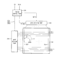
- FIG 1 is a block diagram illustrating an exemplary embodiment of a display apparatus according to the invention.
- FIGS. 2A and 2B are signal timing diagrams illustrating input and output signals of an exemplary embodiment of a timing control part shown in FIG 1 ;
- FIG 3 is a block diagram illustrating an exemplary embodiment of a data driving part shown in FIG 1 ;
- FIG 4 is a signal timing diagram illustrating input and output signals of the data driving part shown in FIG 3 ;
- FIG 5 is a block diagram illustrating an exemplary embodiment of a gate driving part shown in FIG 1 ;
- FIG 6 is a signal timing diagram illustrating input and output signals of the gate driving part shown in FIG 5 ;
- FIGS. 7A, 7B and 7C are schematic diagrams illustrating an exemplary embodiment of a method of driving a display panel shown in FIG 1 ;
- FIGS. 8A, 8B and 8C are schematic diagrams illustrating an alternative exemplary embodiment of a method of driving a display panel according the invention.
- FIGS. 9A, 9B and 9C are schematic diagrams illustrating another alternative exemplary embodiment of a method of driving a display panel according to the invention.
- FIGS. 10A, 10B and 10C are schematic diagrams illustrating still another alternative exemplary embodiment of a method of driving a display panel according to the invention.
- first, second, third etc. may be used herein to describe various elements, components, regions, layers and/or sections, these elements, components, regions, layers and/or sections should not be limited by these terms. These terms are only used to distinguish one element, component, region, layer or section from another element, component, region, layer or section. Thus, a first element, component, region, layer or section discussed below could be termed a second element, component, region, layer or section without departing from the teachings of the present invention.
- relative terms such as “lower” or “bottom” and “upper” or “top,” may be used herein to describe one element's relationship to another element as illustrated in the Figures. It will be understood that relative terms are intended to encompass different orientations of the device in addition to the orientation depicted in the Figures. For example, if the device in one of the figures is turned over, elements described as being on the “lower” side of other elements would then be oriented on “upper” sides of the other elements. The exemplary term “lower,” can therefore, encompasses both an orientation of “lower” and “upper,” depending on the particular orientation of the figure.
- Exemplary embodiments are described herein with reference to cross section illustrations that are schematic illustrations of idealized embodiments. As such, variations from the shapes of the illustrations as a result, for example, of manufacturing techniques and/or tolerances, are to be expected. Thus, embodiments described herein should not be construed as limited to the particular shapes of regions as illustrated herein but are to include deviations in shapes that result, for example, from manufacturing. For example, a region illustrated or described as flat may, typically, have rough and/or nonlinear features. Moreover, sharp angles that are illustrated may be rounded. Thus, the regions illustrated in the figures are schematic in nature and their shapes are not intended to illustrate the precise shape of a region and are not intended to limit the scope of the present claims.
- FIG 1 is a block diagram illustrating an exemplary embodiment of a display apparatus according to the invention.
- FIGS. 2A and 2B are signal timing diagrams illustrating input and output signals of an exemplary embodiment of a timing control part shown in FIG 1 .
- the display apparatus includes a display panel 100, a data driving part 230, a gate driving part 250 and a timing control part 270.
- the display panel 100 includes a plurality of data lines DL1,.., DLm, a plurality of gate lines GL1, GL2,.., GLn crossing the data lines DL1, .., DLm, and a plurality of pixels (n and m are natural numbers).
- the data driving part 230 provides a plurality of data voltages to the data lines DL1, .., DLm.
- the gate driving part 250 provides a plurality of gate signals to the gate lines GL1, GL2, .., GLn.
- the timing control part 270 receives an original control signal CS and a data signal DATA from outside.
- the timing control part 270 generates a data control signal and a gate control signal to control the data driving part 230 and the gate driving part 250 based on the original control signal CS.
- the timing control part 270 provides the data signal DATA to the data driving part 230.
- the original control signal CS includes a three-dimensional ("3D") enable signal 3D_EN, a data enable signal, which is one of a two-dimensional (“2D") data enable signal 2D_DE and a 3D data enable signal 3D_DE, a left-right identification signal LR_S and an odd-even identification signal OE_S, for example.
- the data control signal includes a load signal TP and a reversal signal REV, for example.
- the gate control signal includes a vertical start signal STV, a first gate clock signal CPV1 and a second gate clock signal CPV2, for example.
- the timing control part 270 receives the 2D data enable signal 2D_DE, a 2D image data ID in synchronization with the 2D data enable signal 2D_DE.
- the 2D data enable signal 2D_DE may have a frequency of 120 hertz (Hz).
- the timing control part 270 In the 2D image mode, the timing control part 270 generates a 2D load signal 2D_TP, a 2D reversal signal 2D_REV, a 2D vertical start signal 2D_STV, a first 2D gate clock signal 2D_CPV1 and a second 2D gate clock signal 2D_CPV2 based on the 2D data enable signal 2D_DE.
- a K-th frame FRAME_K includes a vertical active period VA and a vertical blanking period VB.
- the vertical active period VA is a period in which the 2D data enable signal 2D_DE is activated
- the vertical blanking period VB is a period in which the 2D data enable signal 2D_DE is deactivated (K is a natural number).
- the 2D load signal 2D_TP controls an output timing of a data voltage which is an output signal of the data driving part 230 in synchronization with the 2D data enable signal 2D_DE.
- the 2D reversal signal 2D_REV controls a polarity of the data voltage.
- the data voltage may have a positive polarity (+) with respect to a reference voltage.
- the data voltage may have a negative polarity (-) with respect to the reference voltage.
- the 2D reversal signal 2D_REV has a phase reversed every unit frame.
- the 2D reversal signal 2D_REV of a K-th frame FRAME_K has the high level in a first horizontal period and has alternately one of the low level and the high level every two horizontal periods in the remaining horizontal periods, e.g., in a sequence of high level, low level, low level, high level, high level, low level, low level, ..., high level.
- the 2D reversal signal 2D_REV of a (K+1)-th frame FRAME_K+1 has a phase opposite to the phase of the 2D reversal signal 2D_REV of the K-th frame FRAME_K, that is, the 2D reversal signal 2D_REV of the (K+1)-th frame FRAME_K+1 has the low level in the first horizontal period and has alternately one of the high level and the low level every two horizontal periods in the remaining horizontal periods, e.g., in a sequence of low level, high level, high level, low level, low level, high level, high level, ..., low level.
- voltages in a polarity sequence of positive (+), negative (-), negative (-), positive (+), positive (+), negative (-), negative (-), ..., positive (+) may be applied to pixels included in an M-th pixel column during the K-th frame FRAME_K based on the 2D reversal signal 2D_REV (M is a natural number).
- voltages in a polarity sequence of negative (-), positive (+), positive (+), negative (-), negative (-), positive (+), positive (+), ..., negative (-) may be applied to pixels included in the M-th pixel column during the (K+1)-th frame FRAME_K+1.
- the 2D vertical start signal 2D_STV has a frame cycle, and controls a start timing of the gate driving part 250.
- the 2D vertical start signal 2D_STV has a pulse of a high level during an early period of each of the K-th frame FRAME_K and the (K+1)-th frame FRAME_(K+1).
- the first 2D gate clock signal 2D_CPV1 is a control signal to generate odd-numbered gate signals.
- the second 2D gate clock signal 2D_CPV2 is a control signal delayed with respect to the first 2D gate clock signal 2D_CPV1 to generate even-numbered gate signals.
- the first and second 2D gate clock signals 2D_CPV1 and 2D_CPV2 are activated in the vertical active period VA in synchronization with the 2D data enable signal 2D_DE.
- the timing control part 270 receives a 3D data enable signal 3D_DE, a left-right identification signal LR_S, an odd-even identification signal OE_S and 3D stereoscopic image data.
- the 3D data enable signal 3D_DE may have a frequency of 180 Hz.
- the 3D stereoscopic image data includes first-eye data, first-eye partial line data, second-eye data and second-eye partial line data.
- the first-eye may be a left-eye and the second-eye may be a right-eye.
- the first-eye will be referred to as the left-eye and the second-eye will be referred to as the right-eye.
- the partial line data may be one of odd-numbered line data and even-numbered line data among a data frame of a unit frame based on the odd-even identification signal OE_S.
- the partial line data when the odd-even identification signal OE_S is at the low level, the partial line data is the odd-numbered line data, and when the odd-even identification signal OE_S is at high level, the partial line data is even-numbered line data.
- the timing control part 270 generates a 3D load signal 3D_TP, a 3D reversal signal 3D_REV, a 3D vertical start signal 3D_STV, a first 3D gate clock signal 3D_CPV1 and a second 3D gate clock signal 3D_CPV2 based on the 3D data enable signal 3D_DE.
- the K-th frame FRAME_K is temporally divided into a first normal frame N_FRAME1 and a first partial frame P_FRAME1.
- the first normal frame N_FRAME1 is a period corresponding to the vertical active period VA in the 2D image mode shown in FIG 2A , and has a first normal active period NVA1 and a first normal blanking period NVB 1.
- the first normal active period NVA1 may be a period in which the 3D data enable signal 3D_DE is activated, and the left-eye data LD is processed based on the left-right identification signal LR_S.
- the first normal frame N_FRAME1 may have a frequency of 180 Hz.
- the first partial frame P_FRAME1 is a period corresponding to the vertical blanking period VB in the 2D image mode, and has a first partial active period PVA1 and a first partial blanking period PVB 1.
- the first partial active period PVA1 is a period in which the 3D data enable signal 3D_DE is activated and the left-eye odd-numbered line data O_LD is processed based on the odd-even identification signal OE_S.
- the first partial frame P_FRAME1 may have a frequency of 360 Hz.
- the first normal active period NVA1 may be a period in which the left-eye data frame is processed
- the first partial active period PVA1 is a period in which the odd-numbered or the even-numbered line data of the left-eye data frame is processed.
- the first normal blanking period NVB1 and the first partial frame P_FRAME1 may be a period in which a left-eye shutter of shutter glasses is open and a right-eye shutter of the shutter glasses is closed.
- the (K+1)-th frame FRAME_(K+1) is temporally divided into a second normal frame N_FRAME2 and a second partial frame P_FRAME2.
- the second normal frame N_FRAME2 has a second normal active period NVA2 and a second normal blanking period NVB2.
- the right-eye data RD are processed based on the left-right identification signal LR_S during the second normal active period NVA2.
- the second normal frame N_FRAME2 may have a frequency of 180 Hz.
- the second partial frame P_FRAME2 has a second partial active period PVA2 and a second partial blanking period PVB2.
- the right-eye odd-numbered line data O_RD are processed based on the odd-even identification signal OE_S during the second partial active period PVA2.
- the second partial frame P_FRAME1 may have a frequency of 360 Hz.
- the second normal active period NVA2 may be a period in which the right-eye data frame is processed
- the second partial active period PVA2 may be a period in which the odd-numbered line data or the even-numbered line data of the right-eye frame image is processed.
- the second normal blanking period NVB2 and the second partial frame P_FRAME2 may be a period in which the right-eye shutter of the shutter glasses is open and the left-eye shutter of the shutter glasses is closed.
- the 3D load signal 3D_TP controls an output timing of the data voltage, that is, an output signal of the data driving part 230 in synchronization with the 3D data enable signal 3D_DE.
- the 3D reversal signal 3D_REV controls a polarity of the data voltage.
- the 3D reversal signal 3D_REV may have a phase reversed every four frames. As shown FIG 2B , the 3D reversal signal 3D_REV is reversed by a period which includes a first normal frame N_FRAME1, a first partial frame P_FRAME1, a second normal frame N_FRAME2 and a second partial frame P_FRAME2.
- the 3D reversal signal 3D_REV has same phase in the first and second normal frames N_FRAME1 and N_FRAME2 and has a same phase in the first and second partial frames P_FRAME1 and P_FRAME2
- the 3D vertical start signal 3D_STV has a frame cycle, and controls a start timing of the gate driving part 250.
- the 3D vertical start signal 3D_STV has a pulse of a high level during an early period of each of the first normal frame N_FRAME1, the first partial frame P_FRAME1, the second normal frame N_FRAME2 and the second partial frame P_FRAME2.
- the first 3D gate clock signal 3D_CPV1 is a control signal to generate the odd-numbered gate signals.
- the second 3D gate clock signal 3D_CPV2 is a control signal delayed with respect to the first 3D gate clock signal 3D_CPV1 to generate the even-numbered gate signals.
- the first and second 3D gate clock signals 3D_CPV1 and 3D_CPV2 are activated based on the 3D data enable signal 3D_DE and the odd-even identification signal OE_S.
- the odd-numbered gate signals may be applied to the odd-numbered gate line of the display panel 100.
- the odd-even identification signal OE_S may be at the high level
- the second 3D gate clock signal 3D_CPV2 may be activated
- the first 3D gate clock signal 3D_CPV1 may be deactivated.
- the even-numbered gate signals may be applied to the even-numbered gate lines of the display panel 100.
- FIG 3 is a block diagram illustrating an exemplary embodiment of a data driving part shown in FIG 1 .
- the data driving part 230 includes a shift register 231, a latch 232, a digital-to-analog converter (“DAC”) 233 and an output buffer 234.
- DAC digital-to-analog converter
- the shift register 231 provides a latch signal 231a to the latch 232 in parallel based on a data clock signal DCLK.
- the latch 232 sequentially latches data D1, D2, ..., Di-1 and Di in synchronization with the latch signal 231a (i is a natural number).
- the latch 232 latches the data D1, D2, ..., Di-1 and Di on a line-by-line basis and outputs the latched data D1, D2, ..., Di-1 and Di in response to the load signal TP.
- the DAC 233 converts the data D1, D2, ..., Di-1 and Di of the horizontal line unit into data voltages d1, d2, ..., di-1 and di of the positive polarity (+) or the negative polarity (-) using gamma reference voltages +Vref of the positive polarity (+) or the negative polarity (-) based on the reversal signal REV, and outputs the data voltages d1, d2, ..., di-1 and di of the positive polarity (+) or the negative polarity (-).
- the reversal signal REV controls the polarity of the data voltage on a line-by-line basis.
- the output buffer 234 amplifies the data voltages d1, d2, ..., di-1 and di and outputs the amplified data voltages d1, d2, ..., di-1 and di.
- the output buffer 234 may control polarities of the data voltages of the lines based on a preset pixel (or dot) data unit.
- the output buffer 234 when one dot inversion mode is applied to the output buffer 234, the output buffer 234 reverses the polarities of the received data voltages, e.g., +d1, +d2, ..., +di-1, +di, on a dot-by-dot basis outputs the data voltages which are revered as +d1, -d2, ..., +di-1 and -di.
- the output buffer 234 reverses the polarities of the data voltages on a dot-by-dot basis, e.g., the polarities of the data voltages are reversed every dot, but the invention is not limited thereto.
- the DAC 233 may reverse the polarity of the data voltages on a dot-by-dot basis.
- FIG 4 is a signal timing diagram illustrating input and output signals of the data driving part shown in FIG 3 .
- the latch 232 receives left-eye data LD1, LD2, LD3, LD4, LD5, LD6, ... in each horizontal period during the first normal frame N_FRAME1 (IN_DATA).
- the latch 232 outputs the left-eye data LD1, LD2, LD3, LD4, LD5, LD6, ... in each horizontal period to the DAC 233 in synchronization with the load signal TP.
- the DAC 233 converts the left-eye data LD1, LD2, LD3, LD4, LD5, LD6, ... into the data voltages +Ld1, -Ld2, -Ld3, +Ld4, +Ld5, -Ld6, ... of the positive polarity (+) and the negative polarity (-) in response to the reversal signal REV, and outputs the data voltages +Ld1, -Ld2, -Ld3, +Ld4, +Ld5, -Ld6, ... to the output buffer 234.
- the reversal signal REV has a phase corresponding to the 1+2 dot inversion mode.
- the data voltage Ld1 of a first line has the positive polarity (+)
- the data voltages Ld2 and Ld3 of second and third lines have the negative polarity (-)
- the data voltages Ld4 and Ld5 of fourth and fifth lines have the positive polarity (+)
- the data voltages Ld6 and Ld7 of sixth and seventh lines have the negative polarity (-).
- the reversal signal REV controls the polarity of the data voltage on a line-by-line basis.
- the output buffer 234 amplifies the left-eye data voltages +Ld1, -Ld2, -Ld3, +Ld4, +Ld5, -Ld6, ... and outputs the amplified left-eye data voltages +Ld1, -Ld2, -Ld3, +Ld4, +Ld5, -Ld6, ... (OUT_DATA).
- the latch 232 receives the left-eye odd-numbered data LD1, LD3, LD5, ... in each horizontal period (IN_DATA).
- the odd-numbered data correspond to the odd-numbered horizontal line.
- the latch 232 outputs the left-eye odd-numbered data LD1, LD3, LD5, ... in each horizontal period to the DAC 233 in synchronization with the load signal TP.
- the DAC 233 converts the left-eye odd-numbered data LD1, LD3, LD5, ... into the data voltages +Ld1, -Ld3, +Ld5, ... of the positive polarity (+) and the negative polarity (-) in response to the reversal signal REV, and outputs the data voltages +Ld1, -Ld3, +Ld5, ... of the positive polarity (+) and the negative polarity (-) to the output buffer 234.
- the reversal signal REV has a phase corresponding to the one dot inversion mode.
- the data voltage Ld1 of the first horizontal line has the positive polarity (+)
- the data voltage Ld3 of the third horizontal line has the negative polarity (-)
- the data voltage Ld5 of the fifth horizontal line has the positive polarity (+)
- the data voltage Ld7 of the seventh horizontal line has the negative polarity (-).
- the reversal signal REV controls the polarity of the data voltage on a line-by-line basis.
- the output buffer 234 amplifies the left-eye odd-numbered data voltages +Ld1, -Ld3, +Ld5, -Ld7, ... and outputs the amplified left-eye odd-numbered data voltages +Ld1, -Ld3, +Ld5, -Ld7, ... (OUT_DATA).
- the polarities of the left-eye odd-numbered data voltages +Ld1, -Ld3, +Ld5, -Ld7, ... in the first partial frame P_FRAME1, are substantially the same as the polarities of the left-eye odd-numbered data voltages +Ld1, -Ld3, +Ld5, -Ld7, ... in the first normal frame N_FRAME1. Therefore, a view difference between a left-eye image corresponding to the outputted data voltages during the first normal frame N_FRAME1 and a partial left-eye image corresponding to the outputted data voltages during the first partial frame P_FRAME1 is effectively prevented.
- the latch 232 receives right-eye data RD1, RD2, RD3, RD4, RD5, RD6, ... in each horizontal period (IN_DATA) .
- the latch 232 outputs the right-eye data RD1, RD2, RD3, RD4, RD5, RD6, ... in each horizontal period to the DAC 233 in synchronization with the load signal TP.
- the DAC 233 converts the right-eye data RD1, RD2, RD3, RD4, RD5, RD6, ... into the data voltages +Rd1, -Rd2, -Rd3, +Rd4, +Rd5, -Rd6, ... of the positive polarity (+) and the negative polarity (-) in response to the reversal signal REV and outputs the data voltages +Rd1, -Rd2, -Rd3, +Rd4, +Rd5, -Rd6, ... to the output buffer 234.
- the reversal signal REV has a phase corresponding to the 1+2 dot inversion mode.
- the data voltage Rd1 of a first line has the positive polarity (+)
- the data voltages Rd2 and Rd3 of second and third lines have the negative polarity (-)
- the data voltages Rd4 and Rd5 of fourth and fifth lines have the positive polarity (+)
- the data voltages Rd6 and Rd7 of sixth and seventh lines have the negative polarity (-).
- the reversal signal REV controls the polarity of the data voltage on a line-by-line basis.
- the output buffer 234 amplifies the right-eye data voltages +Rd1, -Rd2, -Rd3, +Rd4, +Rd5, -Rd6, ... and outputs the amplified right-eye data voltages +Rd1, -Rd2, -Rd3, +Rd4, +Rd5, -Rd6, ... (OUT_DATA).
- the latch 232 receives the right-eye odd-numbered data RD1, RD3, RD5, ... in each horizontal period (IN_DATA).
- the latch 232 outputs the right-eye odd-numbered data RD1, RD3, RD5, ... in each horizontal period to the DAC 233 in synchronization with the load signal TP.
- the DAC 233 converts the right-eye odd-numbered data RD1, RD3, RD5, ... into the data voltages +Rd1, -Rd3, +Rd5, -Rd7, ... of the positive polarity (+) and the negative polarity (-) in response to the reversal signal REV and outputs the data voltages +Rd1, -Rd3, +Rd5, -Rd7, ... of the positive polarity (+) and the negative polarity (-) to the output buffer 234.
- the reversal signal REV has a phase corresponding to the one dot inversion mode.
- a data voltage Rd1 of the first line has the positive polarity (+)
- a data voltage Rd3 of the third line has the negative polarity (-)
- a data voltage Rd5 of the fifth line has the positive polarity (+)
- a data voltage Rd7 of the seventh line has the negative polarity (-).
- the reversal signal REV controls the polarity of the data voltage on a line-by-line basis.
- the output buffer 234 amplifies the right-eye odd-numbered data voltages +Rd1, -Rd3, +Rd5, -Rd7, ... and outputs the amplified right-eye odd-numbered data voltages +Rd1, -Rd3, +Rd5, -Rd7, ... (OUT_DATA).
- the polarities of the right-eye odd-numbered data voltages +Rd1, -Rd3, +Rd5, -Rd7, ... in the second partial frame P_FRAME2, are substantially the same as the polarities of the right-eye odd-numbered data voltages +Rd1, -Rd3, +Rd5, -Rd7, ... in the second normal frame N_FRAME2. Therefore, a view difference between a right-eye image corresponding to the outputted data voltages during the second normal frame N_FRAME2 and a partial right-eye image corresponding to the outputted data voltages during the second partial frame P_FRAME2 is effectively prevented.
- the reversal signal REV may have a phase corresponding to the 1+2 dot inversion mode (-, +, +, -, -, +, +, ...) opposite to the phase corresponding to the 1+2 dot inversion mode (+, -, -, +, +, -, -, ...) of the first normal frame N_FRAME1.
- the reversal signal REV may have a phase corresponding to the 1 dot inversion mode (-, +, -, +, ...) opposite to the phase corresponding to the 1 dot inversion mode (+, -, +, -, ...) of the first partial frame P_FRAME1.
- the reversal signal REV may have a phase corresponding to the 1+2 dot inversion mode (-, +, +, -,-,+,+,...) opposite to the phase corresponding to the 1+2 dot inversion mode (+, -, -, +, +, -, -, ...) of the second normal frame N_FRAME2.
- the reversal signal REV may have a phase corresponding to the 1 dot inversion mode (-, +, -, +, ...) opposite to the phase corresponding to the 1 dot inversion mode (+, -, +, -, ...) of the second partial frame P_FRAME2.
- the reversal signal REV may have a phase reversed every four frames.
- the polarities of the left-eye data voltages of the first normal frame N_FRAME1 are substantially the same as the polarities of the right-eye data voltages of the second normal frame N_FRAME2.
- the polarities of the left-eye odd-numbered (or even-numbered) data voltages of the first normal frame N_FRAME1 are substantially the same as the polarities of the left-eye odd-numbered (or even-numbered) data voltages of the first partial frame P_FRAME1.
- the polarities of the right-eye odd-numbered (or even-numbered) data voltages of the second normal frame N_FRAME2 are substantially the same as the polarities of the right-eye odd-numbered (or even-numbered) data voltages of the second partial frame P_FRAME2.
- display quality of a 3D stereoscopic image is substantially improved.
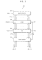
- FIG 5 is a block diagram illustrating an exemplary embodiment of a gate driving part shown in FIG 1 .
- the gate driving part 250 includes a first sub gate circuit 251 and a second sub gate circuit 252.
- the first sub gate circuit 251 includes a plurality of stages SRC11, SRC12, SRC13, .., and receives the vertical start signal STV and the first gate clock signal CPV1.
- the first gate clock signal CPV1 includes a first clock signal CPV11 and a second clock signal CPV12 having a phase opposite to a phase of the first clock signal CPV11.
- Each of the stages SRC11, SRC12, SRC 13, ... includes an input terminal D, a clock terminal CT and an output terminal Q, and may be a data flip flop ("D-FF").
- the input terminal D receives the vertical start signal STV or an output signal of one of previous stages.
- the clock terminal CT receives the first clock signal CPV11 or the second clock signal CPV12.
- an odd-numbered stage SRC11 may receive the first clock signal CPV11 and an even-numbered stage SRC12 may receive the second clock signal CPV12.
- the first clock signal CPV11 may be different from the second clock signal CPV12 and may be a signal delayed with respect to the second clock signal CPV12.
- the output terminal Q outputs a gate signal in synchronization with the first or second clock signal CPV11 or CPV12.
- the first sub gate circuit 251 sequentially outputs odd-numbered gate signals G1, G3, G5, .., Gn-1.
- the second sub gate circuit 252 includes a plurality of stages SRC21, SRC22, SRC23, ... and receives the vertical start signal STV and the second gate clock signal CPV2.
- the second gate clock signal CPV2 receives a third clock signal CPV21 and a fourth clock signal CPV22 having a phase opposite to the phase of the third clock signal CPV21.
- Each of the stages SRC21, SRC22, SRC23, ... includes the input terminal D, the clock terminal CT and the output terminal Q, and may be the D-FF.
- the input terminal D receives the vertical start signal STV or the output signal of one of previous stages.
- the clock terminal CT receives the third clock signal CPV21 or the fourth clock signal CPV22.
- an odd-numbered stage SRC21 may receive the third clock signal CPV21 and an even-numbered stage SRC22 may receive the fourth clock signal CPV22.
- the third clock signal CPV21 may be different from the fourth clock signal CPV22 and may be a signal delayed with respect to the fourth clock signal CPV22.
- the output terminal Q outputs the gate signal in synchronization with the third or fourth clock signal CPV21 or CPV22.
- the second sub gate circuit 252 sequentially outputs even-numbered gate signals G2, G4, G6, .., Gn.
- FIG 6 is a signal timing diagram illustrating input and output signals of the gate driving part shown in FIG 5 .
- the gate driving part 250 receives the vertical start signal STV, the first clock signal CPV11, the second clock signal CPV12, the third clock signal CPV21 and the fourth clock signal CPV22.
- the first sub gate circuit 251 operates in response to the vertical start signal STV and outputs the odd-numbered gate signals G1, G3, G5, .., Gn-1 based on the first and second clock signals CPV11 and CPV12.
- the second sub gate circuit 252 operates in response to the vertical start signal STV and outputs the even-numbered gate signals G2, G4, G6, ..., Gn based on the third and fourth clock signals CPV21 and CPV22.
- the left-eye data LD may be displayed on the display panel 100 during the first normal frame N_FRAME1.
- the gate driving part 250 receives the vertical start signal STV, the first clock signal CPV11 and the second clock signal CPV12, while the timing control part 270 does not provide the third and fourth clock signals CPV21 and CPV22 to the gate driving part 250.
- the first sub gate circuit 251 operates in response to the vertical start signal STV and outputs the odd-numbered gate signals G1, G3, G5, .., Gn-1 based on the first and second clock signals CPV11 and CPV12, while the second sub gate circuit 252 dose not output the even-numbered gate signals G2, G4, G6, .., Gn.
- the left-eye odd-numbered data O_LD may be displayed on the display panel 100 during the first partial frame P_FRAME1.
- the gate driving part 250 receives the vertical start signal STV, the first clock signal CPV11, the second clock signal CPV12, the third clock signal CPV21 and the fourth clock signal CPV22.
- the first sub gate circuit 251 operates in response to the vertical start signal STV and outputs the odd-numbered gate signals G1, G3, G5, ..., Gn-1 based on the first and second clock signals CPV11 and CPV12.
- the second sub gate circuit 252 operates in response to the vertical start signal STV and outputs the even-numbered gate signals G2, G4, G6, ..., Gn based on the third and fourth clock signals CPV21 and CPV22.
- the right-eye data RD may be displayed on the display panel 100 during the second normal frame N_FRAME2.
- the gate driving part 250 receives the vertical start signal STV, the first clock signal CPV11 and the second clock signal CPV12, while the timing control part 270 does not provide the third and fourth clock signals CPV21 and CPV22 to the gate driving part 250.
- the first sub gate circuit 251 operates in response to the vertical start signal STV and outputs the odd-numbered gate signals G1, G3, G5, .., Gn-1 based on the first and second clock signals CPV11 and CPV12, while the second sub gate circuit 252 dose not output the even-numbered gate signals G2, G4, G6, .., Gn.
- the right-eye odd-numbered data O_RD may be displayed on the display panel 100 during the second partial frame P_FRAME2.
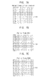
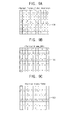
- FIGS. 7A, 7B and 7C are schematic diagrams illustrating an exemplary embodiment of a method of driving a display panel shown in FIG 1 .
- the reversal signal REV when the reversal signal REV has the phase corresponding to the 1+2 dot inversion mode during the normal frame, the reversal signal REV may have a phase corresponding to the one dot inversion mode during the partial frame.
- the voltages may be charged in pixels included in an M-th pixel column of the display panel 100 in a polarity sequence of positive (+), negative (-), negative (-), positive (+), positive (+), negative (-), negative (-), positive (+),... based on the 1+2 dot inversion mode during the normal frame.
- the voltages may be charged in pixels included in the M-th pixel column of the display panel 100 in a polarity sequence of positive (+), negative (-), positive (+), negative (-), ... based on the one dot inversion mode during the partial frame processing odd-numbered data. Therefore, the odd-numbered data voltage of the normal frame and the partial frame may have the same polarities.
- the voltages may be charged in pixels included in the M-th pixel column of the display panel 100 in an order of negative (-), positive (+), negative (-), positive (+), ... voltages based on the one dot inversion mode during the partial frame processing even-numbered data. Therefore, the even-numbered data voltage of the normal frame and the partial frame may have the same polarities.
- FIGS. 8A, 8B and 8C are schematic diagrams illustrating an alternative exemplary embodiment of a method of driving a display panel according to the invention.
- the reversal signal REV when the reversal signal REV has the phase corresponding to the one dot inversion mode during the normal frame, the reversal signal REV may have a phase which is at the high level of the positive polarity (+) or the low level of the negative polarity (-) corresponding to a column inversion mode during the partial frame.
- the voltages may be charged in pixels included in an M-th pixel column of the display panel 100 in a polarity sequence of positive (+), negative (-), positive (+), negative (-), positive (+), negative (-),... voltages according to the 1 dot inversion mode during the normal frame.
- the voltages may be charged in pixels included in the M-th pixel column of the display panel 100 in a polarity sequence of positive (+), positive (+), positive (+), positive (+), ... based on the column inversion mode during the partial frame processing odd-numbered data. Therefore, the odd-numbered data voltage of the normal frame and the partial frame may have the same polarities.
- the voltages may be charged in pixels included in the M-th pixel column of the display panel 100 in a polarity sequence of negative (-), negative (-), negative (-), ... based on the column inversion mode during the partial frame processing even-numbered data. Therefore, the even-numbered data voltage of the normal frame and the partial frame may have the polarities substantially same with each other.
- FIGS. 9A, 9B and 9C are schematic diagrams illustrating another alternative exemplary embodiment of a method of driving a display panel according to the invention.
- the reversal signal REV when the reversal signal REV has the phase corresponding to a 2 dot inversion mode during the normal frame, the reversal signal REV may have the phase corresponding to the 1 dot inversion mode during the partial frame.
- the voltages may be charged in pixels included in an M-th pixel column of the display panel 100 in a polarity sequence of positive (+), negative (-), negative (-), positive (+), positive (+), negative (-), negative (-), positive (+), ... based on the 1+2 dot inversion mode during the normal frame.
- the voltages may be charged in pixels included in the M-th pixel column of the display panel 100 in a polarity sequence of positive (+), negative (-), positive (+), negative (-), ... based on the one dot inversion mode during the partial frame processing odd-numbered data. Therefore, the odd-numbered data voltage of the normal frame and the partial frame may have the same polarities.
- the voltages may be charged in pixels included in the M-th pixel column of the display panel 100 in a polarity sequence of positive (+), negative (-), positive (+), negative (-), ... based on the one dot inversion mode during the partial frame processing even-numbered data. Therefore, the even-numbered data voltage of the normal frame and the partial frame may have the same polarities.
- FIGS. 10A, 10B and 10C are schematic diagrams illustrating still another alternative exemplary embodiment of a method of driving a display panel according the invention.
- the voltages may be charged in pixels included in an M-th pixel column of the display panel 100 in a polarity sequence of positive (+),positive (+), positive (+), positive (+), positive (+), positive (+),... based on the column inversion mode during the normal frame.
- the voltages may be charged in pixels included in the M-th pixel column of the display panel 100 in a polarity sequence of positive (+), positive (+), positive (+), positive (+), positive (+), positive (+),...based on the column inversion mode during the partial frame processing odd-numbered data. Therefore, the odd-numbered data voltage of the normal frame and the partial frame may have the same polarities.
- the voltages may be charged in pixels included in the M-th pixel column of the display panel 100 in a polarity sequence of positive (+),positive (+), positive (+), positive (+), positive (+), positive (+), ... based on the column inversion mode during the partial frame processing even-numbered data. Therefore, the even-numbered data voltage of the normal frame and the partial frame may have the same polarities.
- the reversal signal REV controls the polarity of the data voltage during the partial frame such that the polarity of the data voltage during the partial frame is equal to the polarity of the data voltage during the normal frame. Therefore, deterioration in display quality due to a view difference between an image displayed during the normal frame and an image displayed during the partial frame, such as a flicker and a horizontal line pattern, for example, are effectively prevented, and the display quality is thereby substantially improved.
Landscapes
- Engineering & Computer Science (AREA)
- Multimedia (AREA)
- Signal Processing (AREA)
- Physics & Mathematics (AREA)
- Computer Hardware Design (AREA)
- General Physics & Mathematics (AREA)
- Theoretical Computer Science (AREA)
- Chemical & Material Sciences (AREA)
- Crystallography & Structural Chemistry (AREA)
- Control Of Indicators Other Than Cathode Ray Tubes (AREA)
- Liquid Crystal Display Device Control (AREA)
- Liquid Crystal (AREA)
Applications Claiming Priority (1)
| Application Number | Priority Date | Filing Date | Title |
|---|---|---|---|
| KR1020110046752A KR101818567B1 (ko) | 2011-05-18 | 2011-05-18 | 표시 패널의 구동 방법 및 이를 수행하는 표시 장치 |
Publications (2)
| Publication Number | Publication Date |
|---|---|
| EP2525583A2 true EP2525583A2 (de) | 2012-11-21 |
| EP2525583A3 EP2525583A3 (de) | 2014-05-21 |
Family
ID=45421847
Family Applications (1)
| Application Number | Title | Priority Date | Filing Date |
|---|---|---|---|
| EP11191441.2A Ceased EP2525583A3 (de) | 2011-05-18 | 2011-11-30 | Verfahren zur Ansteuerung einer Anzeigetafel und Anzeigevorrichtung zur Durchführung des Verfahrens |
Country Status (5)
| Country | Link |
|---|---|
| US (1) | US9113158B2 (de) |
| EP (1) | EP2525583A3 (de) |
| JP (1) | JP5964057B2 (de) |
| KR (1) | KR101818567B1 (de) |
| CN (1) | CN102789756B (de) |
Families Citing this family (5)
| Publication number | Priority date | Publication date | Assignee | Title |
|---|---|---|---|---|
| CN102629453B (zh) | 2011-05-25 | 2014-04-30 | 京东方科技集团股份有限公司 | 液晶显示器面板极性反转驱动方法及装置 |
| KR102019764B1 (ko) * | 2012-12-21 | 2019-09-09 | 엘지디스플레이 주식회사 | 액정표시장치 및 그 구동방법 |
| CN103208265B (zh) | 2013-04-15 | 2015-08-19 | 合肥京东方光电科技有限公司 | 液晶显示器件极性反转驱动方法、装置及液晶显示器件 |
| KR20160024048A (ko) | 2014-08-22 | 2016-03-04 | 삼성디스플레이 주식회사 | 표시 장치 |
| KR102335113B1 (ko) * | 2014-12-22 | 2021-12-03 | 삼성디스플레이 주식회사 | 표시 장치 및 그 구동 방법 |
Citations (1)
| Publication number | Priority date | Publication date | Assignee | Title |
|---|---|---|---|---|
| EP2306743A2 (de) * | 2009-09-30 | 2011-04-06 | Sony Corporation | Bildanzeigevorrichtung, Bildanzeigeansichtssystem und Bildanzeigeverfahren |
Family Cites Families (31)
| Publication number | Priority date | Publication date | Assignee | Title |
|---|---|---|---|---|
| JP3155996B2 (ja) * | 1995-12-12 | 2001-04-16 | アルプス電気株式会社 | カラー液晶表示装置 |
| US20010052887A1 (en) | 2000-04-11 | 2001-12-20 | Yusuke Tsutsui | Method and circuit for driving display device |
| JP4218249B2 (ja) * | 2002-03-07 | 2009-02-04 | 株式会社日立製作所 | 表示装置 |
| JP4095518B2 (ja) * | 2002-10-31 | 2008-06-04 | セイコーエプソン株式会社 | 電気光学装置及び電子機器 |
| CN1567419A (zh) * | 2003-06-20 | 2005-01-19 | 统宝光电股份有限公司 | 液晶显示面板的极性反转驱动方法与装置 |
| EP1665212A1 (de) | 2003-09-08 | 2006-06-07 | Koninklijke Philips Electronics N.V. | Aktivierung elektrophoretischer anzeige mit austast-einzelbildern |
| US7576814B2 (en) * | 2004-03-29 | 2009-08-18 | Lg. Display Co., Ltd. | Liquid crystal display device of in-plane switching mode, method of fabricating the same, and method of driving the same |
| KR101090247B1 (ko) * | 2004-04-19 | 2011-12-06 | 삼성전자주식회사 | 4색 표시 장치의 구동 장치 및 방법 |
| JP4572095B2 (ja) * | 2004-07-15 | 2010-10-27 | Nec液晶テクノロジー株式会社 | 液晶表示装置、携帯機器及び液晶表示装置の駆動方法 |
| US7724228B2 (en) * | 2004-11-29 | 2010-05-25 | Lg Display Co., Ltd. | Liquid crystal display device and driving method thereof |
| CN100446079C (zh) * | 2004-12-15 | 2008-12-24 | 日本电气株式会社 | 液晶显示装置、其驱动方法及其驱动电路 |
| US8847861B2 (en) * | 2005-05-20 | 2014-09-30 | Semiconductor Energy Laboratory Co., Ltd. | Active matrix display device, method for driving the same, and electronic device |
| TWI287775B (en) * | 2005-05-30 | 2007-10-01 | Prime View Int Co Ltd | Method for driving liquid crystal display panel |
| TWI298862B (en) * | 2005-10-28 | 2008-07-11 | Novatek Microelectronics Corp | Driving method and data driving circuit of plane surface display |
| JP4883524B2 (ja) * | 2006-03-31 | 2012-02-22 | Nltテクノロジー株式会社 | 液晶表示装置、該液晶表示装置に用いられる駆動制御回路及び駆動方法 |
| KR101315376B1 (ko) * | 2006-08-02 | 2013-10-08 | 삼성디스플레이 주식회사 | 표시 장치의 구동 장치 및 그 영상 신호 보정 방법 |
| KR20080089992A (ko) * | 2007-04-03 | 2008-10-08 | 삼성전자주식회사 | 표시 기판 및 이를 포함하는 액정 표시 장치 |
| KR100859694B1 (ko) | 2007-04-12 | 2008-09-23 | 삼성에스디아이 주식회사 | 평면/입체 액정 표시장치 및 그 구동방법 |
| KR101274702B1 (ko) * | 2007-05-25 | 2013-06-12 | 엘지디스플레이 주식회사 | 액정표시장치와 그 구동방법 |
| KR101330459B1 (ko) * | 2007-12-29 | 2013-11-15 | 엘지디스플레이 주식회사 | 액정표시장치 |
| DE102009002987B4 (de) * | 2008-05-16 | 2018-11-08 | Seereal Technologies S.A. | Steuerbare Vorrichtung zur Phasenmodulation |
| KR101599848B1 (ko) | 2008-11-18 | 2016-03-07 | 엘지전자 주식회사 | 입체 영상 디스플레이 및 그 구동방법 |
| US8390553B2 (en) * | 2009-02-13 | 2013-03-05 | Apple Inc. | Advanced pixel design for optimized driving |
| EP2234100B1 (de) * | 2009-03-26 | 2016-11-02 | Semiconductor Energy Laboratory Co., Ltd. | Flüssigkristallanzeigevorrichtung |
| US8319528B2 (en) * | 2009-03-26 | 2012-11-27 | Semiconductor Energy Laboratory Co., Ltd. | Semiconductor device having interconnected transistors and electronic device including semiconductor device |
| JP2010256420A (ja) * | 2009-04-21 | 2010-11-11 | Sony Corp | 液晶表示装置および液晶表示装置の駆動方法 |
| JP2010266601A (ja) * | 2009-05-13 | 2010-11-25 | Seiko Epson Corp | 電気光学装置及び電子機器 |
| BRPI1010682A2 (pt) * | 2009-05-22 | 2016-03-15 | Sharp Kk | dispositivo de exibição estereoscópica e método para acionar o mesmo |
| JP5629439B2 (ja) * | 2009-08-26 | 2014-11-19 | 株式会社ジャパンディスプレイ | 液晶表示装置 |
| TW201129078A (en) * | 2010-02-01 | 2011-08-16 | Chunghwa Picture Tubes Ltd | Stereoscopic image displaying method |
| TWI410914B (zh) * | 2010-03-12 | 2013-10-01 | Acer Inc | 液晶顯示器及其控制方法 |
-
2011
- 2011-05-18 KR KR1020110046752A patent/KR101818567B1/ko not_active Expired - Fee Related
- 2011-09-23 US US13/242,274 patent/US9113158B2/en not_active Expired - Fee Related
- 2011-11-30 EP EP11191441.2A patent/EP2525583A3/de not_active Ceased
-
2012
- 2012-01-09 CN CN201210008250.0A patent/CN102789756B/zh not_active Expired - Fee Related
- 2012-01-11 JP JP2012003536A patent/JP5964057B2/ja not_active Expired - Fee Related
Patent Citations (1)
| Publication number | Priority date | Publication date | Assignee | Title |
|---|---|---|---|---|
| EP2306743A2 (de) * | 2009-09-30 | 2011-04-06 | Sony Corporation | Bildanzeigevorrichtung, Bildanzeigeansichtssystem und Bildanzeigeverfahren |
Also Published As
| Publication number | Publication date |
|---|---|
| CN102789756B (zh) | 2016-09-07 |
| JP5964057B2 (ja) | 2016-08-03 |
| US20120293495A1 (en) | 2012-11-22 |
| KR101818567B1 (ko) | 2018-02-22 |
| EP2525583A3 (de) | 2014-05-21 |
| KR20120128853A (ko) | 2012-11-28 |
| CN102789756A (zh) | 2012-11-21 |
| JP2012242819A (ja) | 2012-12-10 |
| US9113158B2 (en) | 2015-08-18 |
Similar Documents
| Publication | Publication Date | Title |
|---|---|---|
| KR101477967B1 (ko) | 표시 패널의 구동 방법 및 이를 수행하기 위한 표시 장치 | |
| US8860770B2 (en) | Method of driving a display panel and a display apparatus performing the method | |
| US9196184B2 (en) | Method of driving display panel and display apparatus for performing the same | |
| JP5932316B2 (ja) | 表示装置 | |
| JP5685101B2 (ja) | 立体映像表示装置 | |
| KR101738476B1 (ko) | 표시 패널의 구동 방법 및 이를 수행하는 표시 장치 | |
| US9196220B2 (en) | Three-dimensional image display apparatus and method of driving the same | |
| US20110157161A1 (en) | Method of displaying stereo-scopic image and display apparatus for performing the same | |
| EP2525583A2 (de) | Verfahren zur Ansteuerung einer Anzeigetafel und Anzeigevorrichtung zur Durchführung des Verfahrens | |
| US9875696B2 (en) | Method of displaying three-dimensional image and display apparatus using the same | |
| KR20140000462A (ko) | 표시 장치 및 그것의 입체 영상 표시 방법 | |
| US8803864B2 (en) | Method of driving a display panel and a display apparatus performing the method | |
| US9734777B2 (en) | Display device | |
| KR20150027604A (ko) | 입체 영상 표시 장치 및 그것의 구동 방법 | |
| US20160007013A1 (en) | 3d display method and 3d display device | |
| KR20130028260A (ko) | 표시장치 및 이의 구동방법 | |
| KR20130014194A (ko) | 입체영상 액정표시장치 및 이의 구동방법 |
Legal Events
| Date | Code | Title | Description |
|---|---|---|---|
| PUAI | Public reference made under article 153(3) epc to a published international application that has entered the european phase |
Free format text: ORIGINAL CODE: 0009012 |
|
| AK | Designated contracting states |
Kind code of ref document: A2 Designated state(s): AL AT BE BG CH CY CZ DE DK EE ES FI FR GB GR HR HU IE IS IT LI LT LU LV MC MK MT NL NO PL PT RO RS SE SI SK SM TR |
|
| AX | Request for extension of the european patent |
Extension state: BA ME |
|
| PUAL | Search report despatched |
Free format text: ORIGINAL CODE: 0009013 |
|
| AK | Designated contracting states |
Kind code of ref document: A3 Designated state(s): AL AT BE BG CH CY CZ DE DK EE ES FI FR GB GR HR HU IE IS IT LI LT LU LV MC MK MT NL NO PL PT RO RS SE SI SK SM TR |
|
| AX | Request for extension of the european patent |
Extension state: BA ME |
|
| RIC1 | Information provided on ipc code assigned before grant |
Ipc: H04N 13/04 20060101AFI20140415BHEP Ipc: H04N 13/00 20060101ALI20140415BHEP Ipc: H04N 13/02 20060101ALI20140415BHEP Ipc: G09G 3/36 20060101ALI20140415BHEP |
|
| 17P | Request for examination filed |
Effective date: 20141120 |
|
| RBV | Designated contracting states (corrected) |
Designated state(s): AL AT BE BG CH CY CZ DE DK EE ES FI FR GB GR HR HU IE IS IT LI LT LU LV MC MK MT NL NO PL PT RO RS SE SI SK SM TR |
|
| 17Q | First examination report despatched |
Effective date: 20150601 |
|
| RAP1 | Party data changed (applicant data changed or rights of an application transferred) |
Owner name: SAMSUNG DISPLAY CO., LTD. |
|
| STAA | Information on the status of an ep patent application or granted ep patent |
Free format text: STATUS: THE APPLICATION HAS BEEN REFUSED |
|
| 18R | Application refused |
Effective date: 20170427 |