EP2504873B1 - Strengthened counter electrode of electroluminescent devices - Google Patents
Strengthened counter electrode of electroluminescent devices Download PDFInfo
- Publication number
- EP2504873B1 EP2504873B1 EP10796485.0A EP10796485A EP2504873B1 EP 2504873 B1 EP2504873 B1 EP 2504873B1 EP 10796485 A EP10796485 A EP 10796485A EP 2504873 B1 EP2504873 B1 EP 2504873B1
- Authority
- EP
- European Patent Office
- Prior art keywords
- electrode
- layer
- hard layer
- conductive
- additional hard
- Prior art date
- Legal status (The legal status is an assumption and is not a legal conclusion. Google has not performed a legal analysis and makes no representation as to the accuracy of the status listed.)
- Active
Links
- 239000000463 material Substances 0.000 claims description 43
- 239000000758 substrate Substances 0.000 claims description 32
- 239000003292 glue Substances 0.000 claims description 26
- 238000000151 deposition Methods 0.000 claims description 16
- 238000000034 method Methods 0.000 claims description 14
- 230000008021 deposition Effects 0.000 claims description 13
- 150000004767 nitrides Chemical class 0.000 claims description 8
- 229910044991 metal oxide Inorganic materials 0.000 claims description 6
- 150000004706 metal oxides Chemical class 0.000 claims description 6
- 239000000523 sample Substances 0.000 claims description 4
- 125000006850 spacer group Chemical group 0.000 claims description 4
- 150000002222 fluorine compounds Chemical class 0.000 claims 2
- 239000010410 layer Substances 0.000 description 162
- 229910052751 metal Inorganic materials 0.000 description 14
- 239000002184 metal Substances 0.000 description 14
- 238000002347 injection Methods 0.000 description 9
- 239000007924 injection Substances 0.000 description 9
- VYPSYNLAJGMNEJ-UHFFFAOYSA-N Silicium dioxide Chemical compound O=[Si]=O VYPSYNLAJGMNEJ-UHFFFAOYSA-N 0.000 description 8
- 229910052709 silver Inorganic materials 0.000 description 8
- 150000004673 fluoride salts Chemical class 0.000 description 7
- 238000005229 chemical vapour deposition Methods 0.000 description 6
- 238000002207 thermal evaporation Methods 0.000 description 6
- BQCADISMDOOEFD-UHFFFAOYSA-N Silver Chemical compound [Ag] BQCADISMDOOEFD-UHFFFAOYSA-N 0.000 description 5
- 239000004020 conductor Substances 0.000 description 5
- 238000004519 manufacturing process Methods 0.000 description 5
- 239000002245 particle Substances 0.000 description 5
- 239000004332 silver Substances 0.000 description 5
- GWEVSGVZZGPLCZ-UHFFFAOYSA-N Titan oxide Chemical compound O=[Ti]=O GWEVSGVZZGPLCZ-UHFFFAOYSA-N 0.000 description 4
- 230000003139 buffering effect Effects 0.000 description 4
- 229910052681 coesite Inorganic materials 0.000 description 4
- 229910052906 cristobalite Inorganic materials 0.000 description 4
- 238000005566 electron beam evaporation Methods 0.000 description 4
- 229910052737 gold Inorganic materials 0.000 description 4
- 239000010931 gold Substances 0.000 description 4
- JKQOBWVOAYFWKG-UHFFFAOYSA-N molybdenum trioxide Chemical compound O=[Mo](=O)=O JKQOBWVOAYFWKG-UHFFFAOYSA-N 0.000 description 4
- 229920000642 polymer Polymers 0.000 description 4
- 230000001681 protective effect Effects 0.000 description 4
- 239000000377 silicon dioxide Substances 0.000 description 4
- LIVNPJMFVYWSIS-UHFFFAOYSA-N silicon monoxide Chemical compound [Si-]#[O+] LIVNPJMFVYWSIS-UHFFFAOYSA-N 0.000 description 4
- 229910052682 stishovite Inorganic materials 0.000 description 4
- 229910052905 tridymite Inorganic materials 0.000 description 4
- 102000015933 Rim-like Human genes 0.000 description 3
- 108050004199 Rim-like Proteins 0.000 description 3
- 229910052782 aluminium Inorganic materials 0.000 description 3
- XAGFODPZIPBFFR-UHFFFAOYSA-N aluminium Chemical compound [Al] XAGFODPZIPBFFR-UHFFFAOYSA-N 0.000 description 3
- QVGXLLKOCUKJST-UHFFFAOYSA-N atomic oxygen Chemical compound [O] QVGXLLKOCUKJST-UHFFFAOYSA-N 0.000 description 3
- 239000011248 coating agent Substances 0.000 description 3
- 238000000576 coating method Methods 0.000 description 3
- 239000003086 colorant Substances 0.000 description 3
- 239000005357 flat glass Substances 0.000 description 3
- 239000011888 foil Substances 0.000 description 3
- 239000007789 gas Substances 0.000 description 3
- 239000011521 glass Substances 0.000 description 3
- 239000001301 oxygen Substances 0.000 description 3
- 229910052760 oxygen Inorganic materials 0.000 description 3
- 238000005240 physical vapour deposition Methods 0.000 description 3
- 238000004544 sputter deposition Methods 0.000 description 3
- RYGMFSIKBFXOCR-UHFFFAOYSA-N Copper Chemical compound [Cu] RYGMFSIKBFXOCR-UHFFFAOYSA-N 0.000 description 2
- 239000004593 Epoxy Substances 0.000 description 2
- 230000004888 barrier function Effects 0.000 description 2
- 230000005540 biological transmission Effects 0.000 description 2
- 230000015572 biosynthetic process Effects 0.000 description 2
- XJHCXCQVJFPJIK-UHFFFAOYSA-M caesium fluoride Chemical compound [F-].[Cs+] XJHCXCQVJFPJIK-UHFFFAOYSA-M 0.000 description 2
- WUKWITHWXAAZEY-UHFFFAOYSA-L calcium difluoride Chemical compound [F-].[F-].[Ca+2] WUKWITHWXAAZEY-UHFFFAOYSA-L 0.000 description 2
- 229910001634 calcium fluoride Inorganic materials 0.000 description 2
- 229910052802 copper Inorganic materials 0.000 description 2
- 239000010949 copper Substances 0.000 description 2
- 238000005401 electroluminescence Methods 0.000 description 2
- 230000008020 evaporation Effects 0.000 description 2
- 238000001704 evaporation Methods 0.000 description 2
- 230000005525 hole transport Effects 0.000 description 2
- AMGQUBHHOARCQH-UHFFFAOYSA-N indium;oxotin Chemical compound [In].[Sn]=O AMGQUBHHOARCQH-UHFFFAOYSA-N 0.000 description 2
- 239000002346 layers by function Substances 0.000 description 2
- PQXKHYXIUOZZFA-UHFFFAOYSA-M lithium fluoride Chemical compound [Li+].[F-] PQXKHYXIUOZZFA-UHFFFAOYSA-M 0.000 description 2
- 238000004518 low pressure chemical vapour deposition Methods 0.000 description 2
- 239000011159 matrix material Substances 0.000 description 2
- 150000002739 metals Chemical class 0.000 description 2
- 150000002894 organic compounds Chemical class 0.000 description 2
- 239000012044 organic layer Substances 0.000 description 2
- -1 poly(3,4-ethylendioxythiophene) Polymers 0.000 description 2
- 229920000139 polyethylene terephthalate Polymers 0.000 description 2
- 239000011241 protective layer Substances 0.000 description 2
- 230000003678 scratch resistant effect Effects 0.000 description 2
- 150000003384 small molecules Chemical class 0.000 description 2
- 239000010409 thin film Substances 0.000 description 2
- 238000007740 vapor deposition Methods 0.000 description 2
- RICKKZXCGCSLIU-UHFFFAOYSA-N 2-[2-[carboxymethyl-[[3-hydroxy-5-(hydroxymethyl)-2-methylpyridin-4-yl]methyl]amino]ethyl-[[3-hydroxy-5-(hydroxymethyl)-2-methylpyridin-4-yl]methyl]amino]acetic acid Chemical compound CC1=NC=C(CO)C(CN(CCN(CC(O)=O)CC=2C(=C(C)N=CC=2CO)O)CC(O)=O)=C1O RICKKZXCGCSLIU-UHFFFAOYSA-N 0.000 description 1
- 229920001609 Poly(3,4-ethylenedioxythiophene) Polymers 0.000 description 1
- 239000004411 aluminium Substances 0.000 description 1
- 239000012298 atmosphere Substances 0.000 description 1
- 239000000919 ceramic Substances 0.000 description 1
- 239000003795 chemical substances by application Substances 0.000 description 1
- 229920000547 conjugated polymer Polymers 0.000 description 1
- 238000010168 coupling process Methods 0.000 description 1
- 238000005859 coupling reaction Methods 0.000 description 1
- 239000000412 dendrimer Substances 0.000 description 1
- 229920000736 dendritic polymer Polymers 0.000 description 1
- 230000001419 dependent effect Effects 0.000 description 1
- 238000009792 diffusion process Methods 0.000 description 1
- 230000000694 effects Effects 0.000 description 1
- 238000001017 electron-beam sputter deposition Methods 0.000 description 1
- 238000005538 encapsulation Methods 0.000 description 1
- 230000007613 environmental effect Effects 0.000 description 1
- 239000007888 film coating Substances 0.000 description 1
- 238000009501 film coating Methods 0.000 description 1
- PCHJSUWPFVWCPO-UHFFFAOYSA-N gold Chemical compound [Au] PCHJSUWPFVWCPO-UHFFFAOYSA-N 0.000 description 1
- 239000012212 insulator Substances 0.000 description 1
- 150000002500 ions Chemical class 0.000 description 1
- 238000005259 measurement Methods 0.000 description 1
- 239000000178 monomer Substances 0.000 description 1
- 230000003287 optical effect Effects 0.000 description 1
- 125000002524 organometallic group Chemical group 0.000 description 1
- 238000005325 percolation Methods 0.000 description 1
- 239000004033 plastic Substances 0.000 description 1
- 229920003023 plastic Polymers 0.000 description 1
- 238000002310 reflectometry Methods 0.000 description 1
- 238000006748 scratching Methods 0.000 description 1
- 230000002393 scratching effect Effects 0.000 description 1
- 230000035945 sensitivity Effects 0.000 description 1
- 235000012239 silicon dioxide Nutrition 0.000 description 1
- 239000011343 solid material Substances 0.000 description 1
- 239000002904 solvent Substances 0.000 description 1
- 229910000314 transition metal oxide Inorganic materials 0.000 description 1
- TVIVIEFSHFOWTE-UHFFFAOYSA-K tri(quinolin-8-yloxy)alumane Chemical compound [Al+3].C1=CN=C2C([O-])=CC=CC2=C1.C1=CN=C2C([O-])=CC=CC2=C1.C1=CN=C2C([O-])=CC=CC2=C1 TVIVIEFSHFOWTE-UHFFFAOYSA-K 0.000 description 1
- 229920002554 vinyl polymer Polymers 0.000 description 1
Images
Classifications
-
- H—ELECTRICITY
- H10—SEMICONDUCTOR DEVICES; ELECTRIC SOLID-STATE DEVICES NOT OTHERWISE PROVIDED FOR
- H10K—ORGANIC ELECTRIC SOLID-STATE DEVICES
- H10K50/00—Organic light-emitting devices
- H10K50/80—Constructional details
- H10K50/805—Electrodes
- H10K50/82—Cathodes
-
- H—ELECTRICITY
- H10—SEMICONDUCTOR DEVICES; ELECTRIC SOLID-STATE DEVICES NOT OTHERWISE PROVIDED FOR
- H10K—ORGANIC ELECTRIC SOLID-STATE DEVICES
- H10K50/00—Organic light-emitting devices
-
- H—ELECTRICITY
- H10—SEMICONDUCTOR DEVICES; ELECTRIC SOLID-STATE DEVICES NOT OTHERWISE PROVIDED FOR
- H10K—ORGANIC ELECTRIC SOLID-STATE DEVICES
- H10K50/00—Organic light-emitting devices
- H10K50/10—OLEDs or polymer light-emitting diodes [PLED]
- H10K50/17—Carrier injection layers
- H10K50/171—Electron injection layers
-
- H—ELECTRICITY
- H10—SEMICONDUCTOR DEVICES; ELECTRIC SOLID-STATE DEVICES NOT OTHERWISE PROVIDED FOR
- H10K—ORGANIC ELECTRIC SOLID-STATE DEVICES
- H10K50/00—Organic light-emitting devices
- H10K50/80—Constructional details
- H10K50/805—Electrodes
-
- H—ELECTRICITY
- H10—SEMICONDUCTOR DEVICES; ELECTRIC SOLID-STATE DEVICES NOT OTHERWISE PROVIDED FOR
- H10K—ORGANIC ELECTRIC SOLID-STATE DEVICES
- H10K50/00—Organic light-emitting devices
- H10K50/80—Constructional details
- H10K50/805—Electrodes
- H10K50/82—Cathodes
- H10K50/826—Multilayers, e.g. opaque multilayers
-
- H—ELECTRICITY
- H10—SEMICONDUCTOR DEVICES; ELECTRIC SOLID-STATE DEVICES NOT OTHERWISE PROVIDED FOR
- H10K—ORGANIC ELECTRIC SOLID-STATE DEVICES
- H10K50/00—Organic light-emitting devices
- H10K50/80—Constructional details
- H10K50/805—Electrodes
- H10K50/82—Cathodes
- H10K50/828—Transparent cathodes, e.g. comprising thin metal layers
-
- H—ELECTRICITY
- H10—SEMICONDUCTOR DEVICES; ELECTRIC SOLID-STATE DEVICES NOT OTHERWISE PROVIDED FOR
- H10K—ORGANIC ELECTRIC SOLID-STATE DEVICES
- H10K50/00—Organic light-emitting devices
- H10K50/80—Constructional details
- H10K50/84—Passivation; Containers; Encapsulations
- H10K50/842—Containers
- H10K50/8423—Metallic sealing arrangements
-
- H—ELECTRICITY
- H10—SEMICONDUCTOR DEVICES; ELECTRIC SOLID-STATE DEVICES NOT OTHERWISE PROVIDED FOR
- H10K—ORGANIC ELECTRIC SOLID-STATE DEVICES
- H10K71/00—Manufacture or treatment specially adapted for the organic devices covered by this subclass
-
- H—ELECTRICITY
- H10—SEMICONDUCTOR DEVICES; ELECTRIC SOLID-STATE DEVICES NOT OTHERWISE PROVIDED FOR
- H10K—ORGANIC ELECTRIC SOLID-STATE DEVICES
- H10K2102/00—Constructional details relating to the organic devices covered by this subclass
- H10K2102/301—Details of OLEDs
- H10K2102/302—Details of OLEDs of OLED structures
Definitions
- the invention relates to the field of electroluminescent devices, such as OLED devices, wherein the counter electrode is strengthened by at least two additional layers with a hardness larger than that of the counter electrode.
- Electroluminescent (EL) devices are usually produced by deposition of the electrodes and the required thin electroluminescent layer(s) on a transparent substrate such as glass or a polymer foil through which the light is emitted. When a voltage between around 2 and 10 Volts is applied between the two electrodes the electroluminescent layer or stack of layers emits light.
- the electrode deposited onto the substrate - usually referred to as substrate electrode and also usually forming the anode - can be deposited as thin layer of an electrically conducting but optically transparent oxide, usually indium-tin oxide (ITO).
- ITO indium-tin oxide
- the electrode opposing the substrate electrode - usually referred to as counter electrode and also usually forming the cathode - is generally formed by evaporation of a layer of aluminum or silver with a thickness of around 100 nm after deposition of the electroluminescent layer(s).
- the non-transparent aluminum electrode is replaced by a semitransparent, thin silver electrode.
- transparent EL devices with a transparency of about 2/3, i.e. about 66%, can be produced. These EL devices emit light both from the front, i.e. through the substrate, as well as from the back, i.e. through the silver electrode.
- Both types of counter electrodes are extremely sensitive, so they cannot be touched by a wire etc, e.g. in order to electrically contact the device, without scratching and thus damaging the EL device.
- This sensitivity of the counter electrode is due to the soft metals used as conductor and/or a light reflector.
- These properties of the counter electrode especially lead to the following disadvantageous consequences: Contacting the counter electrode by conductive glue requires either special glues or protective isolating layers between both electrodes, otherwise shorts will develop.
- US 2006/0088951 A1 discloses a method of manufacturing an organic electroluminescent device, which, on a substrate, has a plurality of first electrodes, a light-emitting functional layer disposed to correspond to formation positions of the first electrodes, and a second electrode covering the light-emitting functional layer, includes forming a buffering layer that covers the second electrode, and forming a gas barrier layer that covers the buffering layer.
- the forming of the buffering layer includes coating a coating material having a monomer/ oligomer material and a curing agent under a vacuum atmosphere, without a solvent, and thermally curing the coating material so as to form the buffering layer.
- US 2007/164673 A1 discloses a display device having an electroluminescent display element disposed on a surface of a substrate and a scratch resistant layer disposed over or surrounding the display element.
- the scratch resistant layer has a hardness level of at least 2.5 on Moh's hardness scale.
- US 2007/241665 A1 discloses an organic electroluminescent element in which a luminescent layer is provided between a positive electrode and a negative electrode.
- a buffer layer constituted with a transition metal oxide is provided between the negative electrode and the luminescent layer.
- JP 2005 222733 A discloses an organic electroluminescent element which is provided with a hole injection electrode layer, an electron injection electrode layer, an organic compound layer laid between the hole injection electrode layer and the electron injection electrode layer, and a protection film coating the exposed faces of the electron injection layer 14 and the organic compound layer.
- JP 2007 095518 A discloses an active matrix drive-type organic electroluminescent display device which is equipped with a first electrode formed for every pixel, with a second electrode, with an organic light-emitting medium layer arranged between both electrodes, and with a thin film transistor connected to the first electrode. In a non-pixel region of the second electrode, electrically connected conductive members are provided above the second electrode.
- JP 2003 017245 A discloses an organic EL display panel and a split-drive circuit positioned in a place so that a connecting terminal of the anode side of the split-drive circuit may be joined to the lead-out wiring of the transparent anode electrode side and a connecting terminal of the cathode side may be joined to the lead-out wiring of the cathode electrode side.
- US 2005/0231102 A1 discloses a low reflectivity organic electroluminescence device including organic electroluminescence layers, a transparent electrode, a thin metal electrode, a control layer, and an auxiliary electrode.
- the transparent electrode and the thin metal electrode are sited on both sides of the OEL layer, respectively, in order to excite it to emit light.
- the auxiliary electrode and the thin metal electrode are mostly separated by a control layer. Both the auxiliary electrode and the thin metal electrode are locally connected to maintain electrically connected. Therefore, the control layer is not necessarily conductive and its material selection is not restricted by the requirement of work function matching with adjacent layers.
- a further object of the invention is the provision of a method for the production of such an EL device.
- an EL device comprising a substrate and stacked thereon in the order of mention: a first transparent electrode, an electroluminescent stack and a second electrode, wherein the EL device further comprises at least one additional hard layer that is a), at least one first additional hard layer located underneath the second electrode and consisting of a layer comprising at least one semiconducting metal oxide and b), at least one second additional hard layer located on top of the second electrode, and the first and the second additional hard layers have a hardness larger than the hardness of the second electrode.
- the at least one second additional hard layer is a non-conductive layer and comprises at least one a material selected from the group consisting of oxides, nitrides and fluorides.
- the electroluminescent device further comprises a conductive layer located on top of the hard layer that electrically contacts the second electrode.
- the additional hard layer(s) allow(s) for an assembly of the EL device wherein shorts are prevented. Particularly, it becomes possible to contact the counter electrode using practically any conductive glue available. Even such glues can be used that would require additional protective isolating layers between both electrodes with conventional EL devices.
- the additional hard layer(s) prevent(s) damage to the counter electrode when it is touched by cover lids and/or getter material. Furthermore, due to the less sensitive counter electrode it is now possible to contact the EL device with a probe to check for proper operation. This is extremely advantageous during the production of the EL device in order to select and single out dysfunctional EL devices or such of poor quality.
- the EL device can be any EL device known to the skilled person and/or any device for the generation of light based on electroluminescent diodes.
- the EL device is an organic EL device, i.e. an OLED device.
- the EL device of the present invention is used as or comprised by a light source, a lamp, or is comprised by a monitor, switch or display.
- a light source, a lamp, a monitor, a switch and a display comprising the inventive EL device are encompassed by the present invention.
- the basic structure of an organic EL device is described comprising a substrate and stacked thereon a first transparent electrode, an organic electroluminescent stack, and a second electrode.
- various other basic structures of EL devices, and particularly organic EL devices are known to the skilled person, all of which are meant to be encompassed by the present invention.
- An exemplary basic EL device comprises two electrodes, i.e. an anode and a cathode, wherein the anode is usually disposed on a substrate such as glass or flexible polyethylene terephtalate (PET) foil.
- the EL stack On top of the transparent substrate electrode, the EL stack is disposed comprising at least one emitter layer comprising at least one type of EL molecules.
- a second electrode, i.e. the cathode acting as the counter electrode, is disposed on top of said electroluminescent stack.
- a hole transport layer that may contact the anode
- an electron transport layer that may contact the cathode
- a hole injection layer - preferably made from poly(3,4-ethylendioxythiophene)/polystyrolsulfonate (PEDOT/PSS) - disposed between the anode and the hole transport layer and/or a electron injection layer - preferably a very thin layer made from lithium fluoride, or cesium fluoride - disposed between the electron transport layer and the cathode.
- PEDOT/PSS poly(3,4-ethylendioxythiophene)/polystyrolsulfonate
- a electron injection layer - preferably a very thin layer made from lithium fluoride, or cesium fluoride - disposed between the electron transport layer and the cathode.
- EL devices may comprise an EL stack wherein more than one emitter layer is present.
- the EL device is an OLED device, i.e. the electroluminescent emission layer(s) comprise organic molecules.
- the organic molecules comprise polymers (PLEDs) or small molecules (SMOLEDs).
- the EL device is a phosphorescent organic light-emitting diode (PHOLED) device.
- PLEDs polymers
- SMOLEDs small molecules
- PHOLED phosphorescent organic light-emitting diode
- the present invention is not restricted to specific organic molecules provided such are suitable for the use as electroluminescent molecules in EL devices.
- electroluminescent and/or organic electroluminescent molecules are known to the skilled person, all of which are meant to be encompassed by the present invention.
- electroluminescent molecules preferably mean “organic electroluminescent molecules”.
- the polymers of a PLED are conjugated polymers such as derivates of poly(p-phenylen-vinyls) (PPV) and the small molecules of an SMOLED are organo-metallic chelates, such as for example Alq3, and/or conjugated dendrimers.
- PV poly(p-phenylen-vinyls)
- SMOLED organo-metallic chelates, such as for example Alq3, and/or conjugated dendrimers.
- the substrate preferably is transparent and can comprise any suitable material known to the skilled person.
- transparent refers to the transmission of in the visible range of ⁇ 50 % light in the given material, e.g. the substrate or the electrode. The remaining light is thus either reflected and/or absorbed.
- Transparent includes “semi-transparent” referring to a material that exhibits a transmission of light in the visible range of between ⁇ 10 % and ⁇ 50 %. Thus, whenever reference is made to a "transparent” material this also explicitly discloses a "semi-transparent” material if not stated otherwise.
- Preferably light in the visible range has a wavelength of between ⁇ 450 nm and ⁇ 700 nm.
- a transparent substrate or electrode absorbs and/or reflects less than 50 % of the incident light.
- the substrate is made from glass, plastics, ceramics, and/or comprises at least one of gold and silver.
- Further preferred materials for the substrate comprise polymer sheets or foils, more preferably with a suitable moisture and oxygen barrier to essentially prevent moisture and/or oxygen entering the EL device.
- the substrate may further comprise additional layers, e.g. for optical purposes such as light out-coupling enhancement and the like.
- the substrate can have any suitable geometry, shape or form but is preferably flat and may, if a flexible material is utilized, be shaped or bent into any three-dimensional shape that is required.
- the electrodes can be made from any suitable material known to the skilled person.
- the first electrode i.e. the substrate electrode
- the substrate electrode is a transparent electrode.
- the substrate electrode comprises a transparent conducting oxide (TCO), more preferably indium-tin oxide (ITO), ZnO, or doped ZnO.
- TCO transparent conducting oxide
- ITO indium-tin oxide
- ZnO zinc-doped oxide
- the substrate electrode is undercoated with SiO2 and/or SiO to advantageously suppress diffusion of mobile atoms or ions from the substrate into the electrode.
- Electrodes comprising a TCO preferably have a transparency of > 60 % and ⁇ 100 %, more preferably of ⁇ 70 % and ⁇ 90 % and most preferably of about 80 %.
- the second electrode i.e. the counter electrode
- the second electrode is a non-transparent Al electrode or a transparent Ag or Au electrode.
- such thin-film electrodes have a thickness of about 100 nm in the case of Al and of ⁇ 3 nm and ⁇ 20 nm, more preferably of ⁇ 5 nm and ⁇ 15 nm and most preferably of about ⁇ 8 and ⁇ 10 nm in the case of Ag or Au.
- Transparent electrodes comprising a thin metal layer, such as an Ag or Au layer, preferably have a transparency of > 50 % and ⁇ 100 %, more preferably of > 60 % and ⁇ 80 % and most preferably of about 66 %.
- the first transparent electrode disposed onto the substrate i.e. the front or substrate electrode
- the second transparent electrode disposed onto the EL stack i.e. the counter or back electrode
- the electrodes can be connected to a voltage/current source via electrical conductors.
- the EL stack can be any EL stack known to the skilled person and/or suitable for an EL device. As described above an EL stack comprises at least one EL emitter layer comprising EL molecules. A single EL emitter layer preferably has a thickness of about 10 nm.
- Preferred EL stacks comprise more than one EL layer, each comprising at least one type of EL molecule.
- the EL layers emit light of different colors. This is especially advantageous if color tuneable EL devices are required.
- the EL stack comprises at least two EL emission layers having different emission colors. This means that if the EL device of the present invention is induced to emit light by application of electric voltage/current each of the at least two emission layers will emit light at a different wavelength.
- Each EL emission layer can comprise a single or, more than one type of EL molecules.
- the EL stack comprises three EL emission layers emitting red, green and blue light, respectively.
- the EL device of the present invention comprises at least one second additional hard layer that is located on top of the second electrode.
- Such an additional hard layer has the advantage that the counter electrode is strengthened which results in a less sensitive counter electrode. Additionally, the EL device can be assembled more readily and without generation of shorts: Advantageously, it becomes possible to contact the counter electrode using a multitude of conductive glues that required additional protective isolating layers between both electrodes with conventional EL devices. As further advantages, the additional hard layer prevents cover lids and/or getter material from touching the counter electrode.
- the second hard layer is located on top of the second electrode, i.e. above the second electrode, thus facing away from the first electrode and being positioned further away from the first electrode than the second electrode.
- the second hard layer is directly located on top of the second electrode, i.e. a face of the additional hard layer physically contacts a face of the second electrode.
- At least two additional hard layers are present, wherein the first hard layer is located underneath the second electrode and the second hard layer is located on top of the second electrode. Further hard layers may be present.
- the thickness of the at least one additional hard layer is ⁇ 5 nm and ⁇ 10 ⁇ m, preferably ⁇ 10 nm and ⁇ 10 ⁇ m, even more preferably ⁇ 20 nm and ⁇ 1 ⁇ m.
- the at least first and second additional layers of the EL device of the present invention have a hardness that is larger than the hardness of the second electrode.
- the term "hardness" as used in the present invention refers to the resistance of a solid material to permanent deformation. Hardness can be measured on the Mohs scale or various other scales, such as the Rockwell, Vickers, and Brinell scales. Such methods for the measurement of the hardness of a material are well known to the skilled person.
- the hardness of the additional hard layers is ⁇ 2.75, which is the hardness of Aluminium and ⁇ 10, preferably ⁇ 3 and ⁇ 9, or more preferably ⁇ 3 and ⁇ 7 on the Mohs scale.
- the required thickness and the required hardness of the protective layer(s) depend on the type of conductive glue used. Usually, these glues are non-conductive when employed. During hardening, the polymeric matrix shrinks and presses the conductive particles onto each other in also into intimate contact with the layers to be joined. This shrinkage leads to a formation of percolation paths between the conductive particles and the conductive surfaces to be connected.
- the thickness and hardness of the protective layer depend now on the shrinkage properties of the glue and on the hardness of the conducting particles. In practice, it is easiest to make a thickness series to test which thickness is required for certain conductive glue. With the conductive epoxy CW2400 from Circuit works, a copper layer of about 300 to 400 nm was sufficient to prevent damage to the OLED device.
- the skilled person is aware of a multitude of materials that can be used in order to produce the additional hard layers according to the invention.
- Preferable such materials can be deposited by vapor deposition techniques, more preferably by physical or chemical vapor deposition techniques.
- the material is suitable to be deposited by thermal evaporation, thermal evaporation in vacuum, evaporation by electron-beam evaporation or sputtering.
- the material used for a hard layer that is located on top of the second electrode is a chemically inert material.
- a chemically inert material is fluorides and/or oxides.
- the material used for a hard layer is an electrically non-conducting material, i.e. an insulator.
- the additional hard layer comprises oxides like SiO, SiO 2 , TiO 2 ; nitrides such as SiN; or fluorides such as CaF 2 or MgF. If a non-conductive layer is used for an additional hard layer positioned on top of the second electrode, a covering layer comprising a conductive metal that connects to the underlying second electrode can be used.
- the at least one second additional hard layer is located on top of the second electrode and consists of an electrically non-conductive, i.e. insulating, layer comprising at least one a material selected from the group consisting of oxides, nitrides and fluorides.
- Especially preferred oxides according to the invention are SiO, SiO 2 , or TiO 2 ; an especially preferred nitride according to the invention is SiN; especially preferred fluorides of the invention are CaF 2 and MgF.
- the second hard layer of this embodiment may cover a part of the second electrode or the complete second electrode. Preferably, it covers less than the full area of the second electrode to allow an encapsulation of the hard insulating layer by a further conductive layer, e.g.
- the second hard layer covers the second electrode in a central position and is surrounded by a rim-like area not covering the second electrode.
- the uncovered, rim-like area is then used to contact the second electrode via the further conductive layer.
- the contacting further conductive layer protects the complete second electrode from getter material that may be present in the EL device.
- the EL device further comprises a further conductive layer located on top of the second hard layer that electrically contacts the second electrode.
- the EL device comprises at least one first hard layer that is located underneath the second electrode as described above and at least one second additional hard layer that is located on top of the second electrode as described above -with an additional encapsulating conductive layer.
- the first hard layer located underneath the second electrode consists of a layer comprising at least one semiconducting metal oxide. Surprisingly, such oxides are much harder than the metals of the second electrode. More preferably, this semiconducting metal oxide is selected from the group consisting of MoO 3 , WO 3 and V 2 O 3 .
- Such an arrangement of the first additional hard layer has the advantage that the oxide(s) serve as charge injector(s) for the organic layers.
- the first hard layer of this embodiment preferably is in direct contact with the organic layer.
- the first hard layer of this embodiment may cover a part of the second electrode or the complete second electrode. Preferably, it covers the full area of the second electrode.
- the charge injection effect of the first hard layer located underneath the second electrode is combined with the protective effect of the second hard layer located on top of the second electrode.
- the EL device further comprises cover means to - preferably hermetically - seal the EL device and protect it from environmental influences such as moisture and/or gas, such as oxygen.
- cover means are known to the skilled person and particularly comprise cover lids or cavity lids.
- the cover means is advantageously used to electrically contact the second electrode directly or indirectly and may itself be electrically conductive and/or provide contacting means such as feed-troughs.
- the EL device of the invention may further comprise at least one contacting means arranged to electrically contact the covering means to the second electrode.
- This contacting can be carried out directly or indirectly.
- Various contacting means are known to the skilled, all of which are meant to be encompassed by the present invention.
- Particularly preferred contacting means comprise conductive glue and/or mechanical contacting means.
- Conductive glue can be used to electrically contact the EL device.
- suitable conductive glues are known to the skilled person all of which are encompassed by the present invention.
- An especially preferred glue that can be used is for example "Circuitworks conductive glue CW2400", a two-component epoxy a filling of silver particles. An advantage of this glue is that it is very inexpensive.
- the EL device comprises a mechanical contacting means to electrically contact the second electrode directly or indirectly.
- Such mechanical contacting means comprise conductive spring, posts and/or spacers, preferably soft posts or spacers.
- the cover means encapsulates the EL device and is electrically contacted on the outside.
- the at least one contacting means is connected to the inside of the cover means and touches the second electrode, hard layer located thereon, or additional conductive layer encapsulating the hard layer. Thereby, the EL device is electrically contacted.
- directly contacting describes a direct physical connection between the parts in question.
- directly contacting describes an indirect connection between the parts in question. For example, if a hard layer according to the invention is located on top of the second electrode then a spring used as a contacting means that touches said hard layer indirectly contacts the second electrode electrically, while it directly contacts the hard layer electrically.
- the electroluminescent device according to the invention may further comprise a getter material.
- getter materials are reactive materials used for removing traces of gas and are used to fill the cavity generated by the cover means.
- Preferred getter materials comprise CaO, and/or zeolithes.
- the invention is directed to a method of producing the EL device according to the invention and comprises the steps of: a) providing a substrate; and b) depositing onto the substrate in the order of mention: a first transparent electrode, an electroluminescent stack, and a second electrode, wherein at least one first additional hard layer consisting of a layer comprising at least one semiconducting metal oxide is deposited before deposition of the second electrode, and at least one second additional hard layer is further deposited after the deposition of the second electrode, and wherein the additional hard layers have a hardness larger than the hardness of the second electrode, and wherein the at least one second additional hard layer is a non-conductive layer and comprises at least one a material selected from the group consisting of oxides, nitrides and fluorides, and a conductive layer is deposited on top of the hard layer that electrically contacts the second electrode.
- the deposition steps can be carried out by any suitable means.
- a group of preferred deposition techniques widely known to the skilled person are the vapor deposition techniques.
- Such techniques comprise chemical vapor deposition (CVD), such as low pressure CVD (LPCVD) or physical vapor deposition (PVD), such as sputtering or electron-beam evaporation.
- CVD chemical vapor deposition
- LPCVD low pressure CVD
- PVD physical vapor deposition
- sputtering or electron-beam evaporation such as sputtering or electron-beam evaporation.
- the materials used to produce the additional hard layer located underneath the second electrode are preferably deposited by thermal evaporation in vacuum.
- the materials used to produce the additional hard layer located on top of the second electrode are preferably deposited by thermal evaporation, by electron-beam evaporation or by sputtering.
- the deposition of the at least one hard layer is carried out in a way that the hard layer is located directly underneath and/or on top of the second electrode.
- the deposition of the hard layer can also be carried out so that the hard layer is in contact with the electroluminescent stack.
- the deposition of the at least one hard layer can further be carried out so that the hard layer covers the second electrode partially or completely.
- the required thickness and hardness of the layer depends on the type of glue employed.
- conductive glue 300 - 400 nm of copper were required to prevent damage to the OLED device.
- the skilled person is aware of the possibility to carry out thickness series in order to readily determine the required thickness experimentally.
- a non-conductive layer i.e. an insulating layer, is deposited as a hard layer located on top of the second electrode. At least one material selected from the group consisting of oxides, nitrides and fluorides is deposited in order to produce said layer. A further conductive layer is deposited on top of the hard layer that electrically contacts the second electrode.
- At least two hard layers are deposited, wherein at least one first hard layer is deposited before the deposition of second electrode and at least one second hard layer is deposited after the deposition of the second electrode.
- the method further comprises the step of temporarily contacting the EL device with a probe to check for proper operation of the device.
- the protecting hard layer on top of the second electrode is contacted by the probe, i.e. the contacting is carried out after deposition of this hard layer.
- the method further comprises applying a cover means, at least one contacting means and/or a getter material to the EL device.
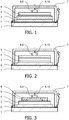
- Fig. 1 is a schematic cross-sectional view of an EL device.
- the EL device depicted is an OLED device and comprises a flat glass substrate 1 onto which a transparent ITO anode 2 has been deposited by CVD. On top of the electrode an OLED stack 3 and an Al cathode 4 have been deposited. The cathode has a thickness of about 100 nm.
- the OLED device has been encapsulated by a cavity lid serving as cover means 7 to hermetically seal the device.
- the OLED device is electrically contacted via the cavity lid and the cathode, respectively.
- the cavity lid is made from a conductive material, i.e. a metal, and electrically contacts the cathode indirectly via two contacting means 8, i.e. conductive glue 9 that has been directly applied to the cathode and a conductive spring 10 that touches both cavity lid and conductive glue.
- a single hard layer 5 comprising MoO 3 , with a thickness of about 100 nm and has been deposited directly underneath the cathode by thermal evaporation of the material in vacuum and completely covers the lower face of the cathode.
- the hard layer is in contact with the cathode. Furthermore, the hard layer contacts the OLED stack and thus provides for a charge injection into the electroluminescent stack.
- Fig. 2 is a schematic cross-sectional view of another EL device.
- the depicted EL device is an OLED device that comprises a flat glass substrate 1 onto which a transparent ITO anode 2 has been deposited by CVD. On top of this first electrode an electroluminescent stack 3 and an Ag cathode 4 have been deposited. The cathode has a thickness of about 100 nm.
- the OLED device has been encapsulated by a cavity lid serving as cover means 7 to hermetically seal the device.
- the OLED device of Fig. 2 is electrically contacted via the cavity lid and the cathode, respectively.
- the cavity lid is made from a conductive material, i.e. a metal, and electrically contacts the cathode indirectly via two contacting means 8 and hard layer 5.
- the contacting means are conductive glue 9 that has been directly applied to the single conductive hard layer and a conductive post 10 that touches both cavity lid and conductive glue.
- the single conductive hard layer 5 comprises WO 3 and has a thickness of about 100 nm. It has been deposited directly on top of the cathode by electron-beam or thermal evaporation completely covering the upper face of the cathode. The hard layer is in contact with the cathode and protectively covers the sensitive electrode.
- a getter material (not shown) is present in the cavity created by the cavity lid.
- Fig. 3 is a schematic cross-sectional view of an other EL device.
- the depicted EL device is an OLED device that comprises a flat glass substrate 1 onto which a transparent ITO anode 2 has been deposited by CVD. On top of this first electrode an electroluminescent stack 3 and an Ag cathode 4 have been deposited. The cathode has a thickness of about 100 nm.
- the OLED device has been encapsulated by a cavity lid serving as cover means 7 to hermetically seal the device.
- the OLED device of Fig. 3 is electrically contacted via the cavity lid and the cathode, respectively.
- the cavity lid is made from metal and electrically contacts the anode indirectly via two contacting means 8 and an additional conductive metal layer 6.
- the contacting means are conductive glue 9 that has been directly applied to the additional conductive layer 6 and a conductive spacer 10 that touches both cavity lid and conductive glue.
- the single non-conductive hard layer 5 comprises SiO 2 and has a thickness of about 100 nm and a. It has been deposited directly on top of the cathode by sputtering and only partially covers the cathode. The hard layer is in contact with the cathode and protectively covers this sensitive electrode, while the encapsulating additional conductive metal layer 6 contacts the cathode in the places that are not covered by the non-conductive hard layer, thus providing for an electrical connection.
Landscapes
- Physics & Mathematics (AREA)
- Optics & Photonics (AREA)
- Engineering & Computer Science (AREA)
- Manufacturing & Machinery (AREA)
- Electroluminescent Light Sources (AREA)
Description
- The invention relates to the field of electroluminescent devices, such as OLED devices, wherein the counter electrode is strengthened by at least two additional layers with a hardness larger than that of the counter electrode.
- Conventional electroluminescent (EL) devices are usually produced by deposition of the electrodes and the required thin electroluminescent layer(s) on a transparent substrate such as glass or a polymer foil through which the light is emitted. When a voltage between around 2 and 10 Volts is applied between the two electrodes the electroluminescent layer or stack of layers emits light.
- In such EL devices the electrode deposited onto the substrate - usually referred to as substrate electrode and also usually forming the anode - can be deposited as thin layer of an electrically conducting but optically transparent oxide, usually indium-tin oxide (ITO). The electrode opposing the substrate electrode - usually referred to as counter electrode and also usually forming the cathode - is generally formed by evaporation of a layer of aluminum or silver with a thickness of around 100 nm after deposition of the electroluminescent layer(s).
- In another type of EL device, the non-transparent aluminum electrode is replaced by a semitransparent, thin silver electrode. In this case, transparent EL devices with a transparency of about 2/3, i.e. about 66%, can be produced. These EL devices emit light both from the front, i.e. through the substrate, as well as from the back, i.e. through the silver electrode.
- Both types of counter electrodes are extremely sensitive, so they cannot be touched by a wire etc, e.g. in order to electrically contact the device, without scratching and thus damaging the EL device. This sensitivity of the counter electrode is due to the soft metals used as conductor and/or a light reflector. These properties of the counter electrode especially lead to the following disadvantageous consequences:
Contacting the counter electrode by conductive glue requires either special glues or protective isolating layers between both electrodes, otherwise shorts will develop. - When a cover lid that is often used with such EL devices touches the counter electrode even slightly, shorts will develop.
- When getter material touches the counter electrode, shorts will develop.
-
US 2006/0088951 A1 discloses a method of manufacturing an organic electroluminescent device, which, on a substrate, has a plurality of first electrodes, a light-emitting functional layer disposed to correspond to formation positions of the first electrodes, and a second electrode covering the light-emitting functional layer, includes forming a buffering layer that covers the second electrode, and forming a gas barrier layer that covers the buffering layer. The forming of the buffering layer includes coating a coating material having a monomer/ oligomer material and a curing agent under a vacuum atmosphere, without a solvent, and thermally curing the coating material so as to form the buffering layer. -
US 2007/164673 A1 discloses a display device having an electroluminescent display element disposed on a surface of a substrate and a scratch resistant layer disposed over or surrounding the display element. The scratch resistant layer has a hardness level of at least 2.5 on Moh's hardness scale. -
US 2007/241665 A1 discloses an organic electroluminescent element in which a luminescent layer is provided between a positive electrode and a negative electrode. A buffer layer constituted with a transition metal oxide is provided between the negative electrode and the luminescent layer. -
JP 2005 222733 A -
JP 2007 095518 A -
JP 2003 017245 A -
US 2005/0231102 A1 discloses a low reflectivity organic electroluminescence device including organic electroluminescence layers, a transparent electrode, a thin metal electrode, a control layer, and an auxiliary electrode. The transparent electrode and the thin metal electrode are sited on both sides of the OEL layer, respectively, in order to excite it to emit light. The auxiliary electrode and the thin metal electrode are mostly separated by a control layer. Both the auxiliary electrode and the thin metal electrode are locally connected to maintain electrically connected. Therefore, the control layer is not necessarily conductive and its material selection is not restricted by the requirement of work function matching with adjacent layers. - It is an object of the invention to provide an EL device with a strengthened and thus less sensitive counter electrode. A further object of the invention is the provision of a method for the production of such an EL device.
- This object is achieved by an EL device and the method according to the appended independent claims. In particular, an EL device is provided comprising a substrate and stacked thereon in the order of mention: a first transparent electrode, an electroluminescent stack and a second electrode, wherein the EL device further comprises at least one additional hard layer that is a), at least one first additional hard layer located underneath the second electrode and consisting of a layer comprising at least one semiconducting metal oxide and b), at least one second additional hard layer located on top of the second electrode, and the first and the second additional hard layers have a hardness larger than the hardness of the second electrode. The at least one second additional hard layer is a non-conductive layer and comprises at least one a material selected from the group consisting of oxides, nitrides and fluorides. The electroluminescent device further comprises a conductive layer located on top of the hard layer that electrically contacts the second electrode. By means of such additional hard layers the second electrode, i.e. the counter electrode, is advantageously strengthened, resulting in a less sensitive counter electrode.
- Furthermore, the additional hard layer(s) allow(s) for an assembly of the EL device wherein shorts are prevented. Particularly, it becomes possible to contact the counter electrode using practically any conductive glue available. Even such glues can be used that would require additional protective isolating layers between both electrodes with conventional EL devices. In addition, the additional hard layer(s) prevent(s) damage to the counter electrode when it is touched by cover lids and/or getter material. Furthermore, due to the less sensitive counter electrode it is now possible to contact the EL device with a probe to check for proper operation. This is extremely advantageous during the production of the EL device in order to select and single out dysfunctional EL devices or such of poor quality.
- The EL device can be any EL device known to the skilled person and/or any device for the generation of light based on electroluminescent diodes. Preferably the EL device is an organic EL device, i.e. an OLED device. In further embodiments the EL device of the present invention is used as or comprised by a light source, a lamp, or is comprised by a monitor, switch or display. Thus, also a light source, a lamp, a monitor, a switch and a display comprising the inventive EL device are encompassed by the present invention. In the following the basic structure of an organic EL device is described comprising a substrate and stacked thereon a first transparent electrode, an organic electroluminescent stack, and a second electrode. However, various other basic structures of EL devices, and particularly organic EL devices, are known to the skilled person, all of which are meant to be encompassed by the present invention.
- An exemplary basic EL device comprises two electrodes, i.e. an anode and a cathode, wherein the anode is usually disposed on a substrate such as glass or flexible polyethylene terephtalate (PET) foil. On top of the transparent substrate electrode, the EL stack is disposed comprising at least one emitter layer comprising at least one type of EL molecules. A second electrode, i.e. the cathode acting as the counter electrode, is disposed on top of said electroluminescent stack. The skilled person will be aware of the fact that various other layers may be incorporated for the production of such an EL device, for example, a hole transport layer that may contact the anode, an electron transport layer that may contact the cathode, a hole injection layer - preferably made from poly(3,4-ethylendioxythiophene)/polystyrolsulfonate (PEDOT/PSS) - disposed between the anode and the hole transport layer and/or a electron injection layer - preferably a very thin layer made from lithium fluoride, or cesium fluoride - disposed between the electron transport layer and the cathode. Furthermore, it is known to the skilled person that EL devices may comprise an EL stack wherein more than one emitter layer is present.
- In one embodiment the EL device is an OLED device, i.e. the electroluminescent emission layer(s) comprise organic molecules. In further preferred embodiments the organic molecules comprise polymers (PLEDs) or small molecules (SMOLEDs). In another preferred embodiment, the EL device is a phosphorescent organic light-emitting diode (PHOLED) device. The present invention is not restricted to specific organic molecules provided such are suitable for the use as electroluminescent molecules in EL devices. Various electroluminescent and/or organic electroluminescent molecules are known to the skilled person, all of which are meant to be encompassed by the present invention. As used in the present invention "electroluminescent molecules" preferably mean "organic electroluminescent molecules". In preferred embodiments the polymers of a PLED are conjugated polymers such as derivates of poly(p-phenylen-vinyls) (PPV) and the small molecules of an SMOLED are organo-metallic chelates, such as for example Alq3, and/or conjugated dendrimers.
- The substrate preferably is transparent and can comprise any suitable material known to the skilled person. In the present invention the term "transparent" refers to the transmission of in the visible range of ≥ 50 % light in the given material, e.g. the substrate or the electrode. The remaining light is thus either reflected and/or absorbed. "Transparent" includes "semi-transparent" referring to a material that exhibits a transmission of light in the visible range of between ≥ 10 % and < 50 %. Thus, whenever reference is made to a "transparent" material this also explicitly discloses a "semi-transparent" material if not stated otherwise. Preferably light in the visible range has a wavelength of between ≥ 450 nm and ≤ 700 nm. Thus, for example, a transparent substrate or electrode absorbs and/or reflects less than 50 % of the incident light.
- In preferred embodiments of the invention the substrate is made from glass, plastics, ceramics, and/or comprises at least one of gold and silver. Further preferred materials for the substrate comprise polymer sheets or foils, more preferably with a suitable moisture and oxygen barrier to essentially prevent moisture and/or oxygen entering the EL device. The substrate may further comprise additional layers, e.g. for optical purposes such as light out-coupling enhancement and the like.
- The substrate can have any suitable geometry, shape or form but is preferably flat and may, if a flexible material is utilized, be shaped or bent into any three-dimensional shape that is required.
- The electrodes can be made from any suitable material known to the skilled person.
- In a preferred embodiment the first electrode, i.e. the substrate electrode, is a transparent electrode. In a further preferred embodiment of the invention the substrate electrode comprises a transparent conducting oxide (TCO), more preferably indium-tin oxide (ITO), ZnO, or doped ZnO. Optionally the substrate electrode is undercoated with SiO2 and/or SiO to advantageously suppress diffusion of mobile atoms or ions from the substrate into the electrode. Electrodes comprising a TCO preferably have a transparency of > 60 % and ≤ 100 %, more preferably of ≥ 70 % and ≤ 90 % and most preferably of about 80 %.
- In further embodiments of the invention the second electrode, i.e. the counter electrode, is a non-transparent Al electrode or a transparent Ag or Au electrode. Preferably, such thin-film electrodes have a thickness of about 100 nm in the case of Al and of ≥ 3 nm and ≤ 20 nm, more preferably of ≥ 5 nm and ≤ 15 nm and most preferably of about ≥ 8 and ≤ 10 nm in the case of Ag or Au.
- Transparent electrodes comprising a thin metal layer, such as an Ag or Au layer, preferably have a transparency of > 50 % and ≤ 100 %, more preferably of > 60 % and ≤ 80 % and most preferably of about 66 %.
- In a further preferred embodiment the first transparent electrode disposed onto the substrate, i.e. the front or substrate electrode, is the anode and the second transparent electrode disposed onto the EL stack, i.e. the counter or back electrode, is the cathode.
- The electrodes can be connected to a voltage/current source via electrical conductors.
- The EL stack can be any EL stack known to the skilled person and/or suitable for an EL device. As described above an EL stack comprises at least one EL emitter layer comprising EL molecules. A single EL emitter layer preferably has a thickness of about 10 nm.
- Preferred EL stacks comprise more than one EL layer, each comprising at least one type of EL molecule. Preferably, the EL layers emit light of different colors. This is especially advantageous if color tuneable EL devices are required. In a further embodiment of the invention the EL stack comprises at least two EL emission layers having different emission colors. This means that if the EL device of the present invention is induced to emit light by application of electric voltage/current each of the at least two emission layers will emit light at a different wavelength.
- Different emission colors are usually achieved by use of different EL molecules that are comprised by the EL emission layers. Each EL emission layer can comprise a single or, more than one type of EL molecules. In more preferred embodiments, the EL stack comprises three EL emission layers emitting red, green and blue light, respectively.
- The EL device of the present invention comprises at least one second additional hard layer that is located on top of the second electrode. Such an additional hard layer has the advantage that the counter electrode is strengthened which results in a less sensitive counter electrode. Additionally, the EL device can be assembled more readily and without generation of shorts: Advantageously, it becomes possible to contact the counter electrode using a multitude of conductive glues that required additional protective isolating layers between both electrodes with conventional EL devices. As further advantages, the additional hard layer prevents cover lids and/or getter material from touching the counter electrode.
- The second hard layer is located on top of the second electrode, i.e. above the second electrode, thus facing away from the first electrode and being positioned further away from the first electrode than the second electrode.
- In a preferred embodiment the second hard layer is directly located on top of the second electrode, i.e. a face of the additional hard layer physically contacts a face of the second electrode.
- At least two additional hard layers are present, wherein the first hard layer is located underneath the second electrode and the second hard layer is located on top of the second electrode. Further hard layers may be present.
- In a further embodiment of the invention the thickness of the at least one additional hard layer is ≥ 5 nm and ≤ 10 µm, preferably ≥ 10 nm and ≤ 10 µm, even more preferably ≥ 20 nm and ≤ 1 µm.
- The at least first and second additional layers of the EL device of the present invention have a hardness that is larger than the hardness of the second electrode. The term "hardness" as used in the present invention refers to the resistance of a solid material to permanent deformation. Hardness can be measured on the Mohs scale or various other scales, such as the Rockwell, Vickers, and Brinell scales. Such methods for the measurement of the hardness of a material are well known to the skilled person.
- In another preferred embodiment the hardness of the additional hard layers is ≥ 2.75, which is the hardness of Aluminium and ≤ 10, preferably ≥ 3 and ≤ 9, or more preferably ≥ 3 and ≤ 7 on the Mohs scale.
- The required thickness and the required hardness of the protective layer(s) depend on the type of conductive glue used. Usually, these glues are non-conductive when employed. During hardening, the polymeric matrix shrinks and presses the conductive particles onto each other in also into intimate contact with the layers to be joined. This shrinkage leads to a formation of percolation paths between the conductive particles and the conductive surfaces to be connected. The thickness and hardness of the protective layer depend now on the shrinkage properties of the glue and on the hardness of the conducting particles. In practice, it is easiest to make a thickness series to test which thickness is required for certain conductive glue. With the conductive epoxy CW2400 from Circuit works, a copper layer of about 300 to 400 nm was sufficient to prevent damage to the OLED device.
- The skilled person is aware of a multitude of materials that can be used in order to produce the additional hard layers according to the invention. Preferable such materials can be deposited by vapor deposition techniques, more preferably by physical or chemical vapor deposition techniques. In further preferred embodiments the material is suitable to be deposited by thermal evaporation, thermal evaporation in vacuum, evaporation by electron-beam evaporation or sputtering.
- In a preferred embodiment of the invention the material used for a hard layer that is located on top of the second electrode is a chemically inert material. This has the advantages that a large selection of conductive glues which otherwise would destroy the second electrode can be used and that getter particles of getter material is kept from coming in contact with the second electrode. Especially preferred examples for chemically inert materials that may be used for the additional hard layer are fluorides and/or oxides.
- The material used for a hard layer is an electrically non-conducting material, i.e. an insulator.
- In preferred embodiments of the invention the additional hard layer comprises oxides like SiO, SiO2, TiO2; nitrides such as SiN; or fluorides such as CaF2 or MgF. If a non-conductive layer is used for an additional hard layer positioned on top of the second electrode, a covering layer comprising a conductive metal that connects to the underlying second electrode can be used.
- The at least one second additional hard layer is located on top of the second electrode and consists of an electrically non-conductive, i.e. insulating, layer comprising at least one a material selected from the group consisting of oxides, nitrides and fluorides. Especially preferred oxides according to the invention are SiO, SiO2, or TiO2; an especially preferred nitride according to the invention is SiN; especially preferred fluorides of the invention are CaF2 and MgF. The second hard layer of this embodiment may cover a part of the second electrode or the complete second electrode. Preferably, it covers less than the full area of the second electrode to allow an encapsulation of the hard insulating layer by a further conductive layer, e.g. a metal layer, that contacts the second electrode. Thus, most preferably the second hard layer covers the second electrode in a central position and is surrounded by a rim-like area not covering the second electrode. The uncovered, rim-like area is then used to contact the second electrode via the further conductive layer. Advantageously, if the rim-like area is as small as possible and located in the outermost perimeter of the second electrode, the contacting further conductive layer protects the complete second electrode from getter material that may be present in the EL device.
- The EL device further comprises a further conductive layer located on top of the second hard layer that electrically contacts the second electrode.
- The EL device comprises at least one first hard layer that is located underneath the second electrode as described above and at least one second additional hard layer that is located on top of the second electrode as described above -with an additional encapsulating conductive layer. The first hard layer located underneath the second electrode consists of a layer comprising at least one semiconducting metal oxide. Surprisingly, such oxides are much harder than the metals of the second electrode. More preferably, this semiconducting metal oxide is selected from the group consisting of MoO3, WO3 and V2O3. Such an arrangement of the first additional hard layer has the advantage that the oxide(s) serve as charge injector(s) for the organic layers. Thus, the first hard layer of this embodiment preferably is in direct contact with the organic layer. The first hard layer of this embodiment may cover a part of the second electrode or the complete second electrode. Preferably, it covers the full area of the second electrode. Thus, advantageously the charge injection effect of the first hard layer located underneath the second electrode is combined with the protective effect of the second hard layer located on top of the second electrode.
- In another embodiment of the invention the EL device further comprises cover means to - preferably hermetically - seal the EL device and protect it from environmental influences such as moisture and/or gas, such as oxygen. A wide selection of cover means are known to the skilled person and particularly comprise cover lids or cavity lids. The cover means is advantageously used to electrically contact the second electrode directly or indirectly and may itself be electrically conductive and/or provide contacting means such as feed-troughs.
- The EL device of the invention may further comprise at least one contacting means arranged to electrically contact the covering means to the second electrode. This contacting can be carried out directly or indirectly. Various contacting means are known to the skilled, all of which are meant to be encompassed by the present invention. Particularly preferred contacting means comprise conductive glue and/or mechanical contacting means.
- Conductive glue can be used to electrically contact the EL device. A multitude of suitable conductive glues are known to the skilled person all of which are encompassed by the present invention. Advantageously, if the second electrode is protected by an additional hard layer that is located on top of the second electrode then a wide selection of conductive glues which otherwise would destroy the second electrode can be used. An especially preferred glue that can be used is for example "Circuitworks conductive glue CW2400", a two-component epoxy a filling of silver particles. An advantage of this glue is that it is very inexpensive.
- In another embodiment of the invention the EL device comprises a mechanical contacting means to electrically contact the second electrode directly or indirectly. Such mechanical contacting means comprise conductive spring, posts and/or spacers, preferably soft posts or spacers.
- Preferably, the cover means encapsulates the EL device and is electrically contacted on the outside. The at least one contacting means is connected to the inside of the cover means and touches the second electrode, hard layer located thereon, or additional conductive layer encapsulating the hard layer. Thereby, the EL device is electrically contacted.
- The term "directly contacting" as used herein, describes a direct physical connection between the parts in question. The term "indirectly contacting" as used herein describes an indirect connection between the parts in question. For example, if a hard layer according to the invention is located on top of the second electrode then a spring used as a contacting means that touches said hard layer indirectly contacts the second electrode electrically, while it directly contacts the hard layer electrically.
- The electroluminescent device according to the invention may further comprise a getter material. As known to the skilled person, getter materials are reactive materials used for removing traces of gas and are used to fill the cavity generated by the cover means. Preferred getter materials comprise CaO, and/or zeolithes. As a contacting of the getter material with the second electrode is to be prevented the hard layer according to the invention covering the second electrode advantageously protects the sensitive electrode.
- In another aspect, the invention is directed to a method of producing the EL device according to the invention and comprises the steps of: a) providing a substrate; and b) depositing onto the substrate in the order of mention: a first transparent electrode, an electroluminescent stack, and a second electrode, wherein at least one first additional hard layer consisting of a layer comprising at least one semiconducting metal oxide is deposited before deposition of the second electrode, and at least one second additional hard layer is further deposited after the deposition of the second electrode, and wherein the additional hard layers have a hardness larger than the hardness of the second electrode, and wherein the at least one second additional hard layer is a non-conductive layer and comprises at least one a material selected from the group consisting of oxides, nitrides and fluorides, and a conductive layer is deposited on top of the hard layer that electrically contacts the second electrode.
- The deposition steps can be carried out by any suitable means. A group of preferred deposition techniques widely known to the skilled person are the vapor deposition techniques. Such techniques comprise chemical vapor deposition (CVD), such as low pressure CVD (LPCVD) or physical vapor deposition (PVD), such as sputtering or electron-beam evaporation.
- The materials used to produce the additional hard layer located underneath the second electrode are preferably deposited by thermal evaporation in vacuum.
- The materials used to produce the additional hard layer located on top of the second electrode are preferably deposited by thermal evaporation, by electron-beam evaporation or by sputtering.
- Preferred embodiments of the method according to the invention will be readily apparent to the skilled person when reading the description regarding the EL device above. However, in the following some of the preferred embodiments will explicitly be disclosed.
- In one embodiment the deposition of the at least one hard layer is carried out in a way that the hard layer is located directly underneath and/or on top of the second electrode. The deposition of the hard layer can also be carried out so that the hard layer is in contact with the electroluminescent stack.
- The deposition of the at least one hard layer can further be carried out so that the hard layer covers the second electrode partially or completely.
- As explained above, the required thickness and hardness of the layer depends on the type of glue employed. For the Circuitworks conductive glue, 300 - 400 nm of copper were required to prevent damage to the OLED device. The skilled person is aware of the possibility to carry out thickness series in order to readily determine the required thickness experimentally.
- A non-conductive layer, i.e. an insulating layer, is deposited as a hard layer located on top of the second electrode. At least one material selected from the group consisting of oxides, nitrides and fluorides is deposited in order to produce said layer. A further conductive layer is deposited on top of the hard layer that electrically contacts the second electrode.
- At least two hard layers are deposited, wherein at least one first hard layer is deposited before the deposition of second electrode and at least one second hard layer is deposited after the deposition of the second electrode.
- In another embodiment of the invention the method further comprises the step of temporarily contacting the EL device with a probe to check for proper operation of the device. Preferably, the protecting hard layer on top of the second electrode is contacted by the probe, i.e. the contacting is carried out after deposition of this hard layer. This has the advantage that during the production of the EL device dysfunctional EL devices or EL devices of poor quality can be detected and singled out.
- In even another embodiment of the invention the method further comprises applying a cover means, at least one contacting means and/or a getter material to the EL device.
- These and other aspects of the invention will be apparent from and elucidated with reference to the embodiments described hereinafter.
- In the drawings:
-
Fig. 1 shows a schematic cross-sectional view of an EL device, not according to the claimed invention. -
Fig. 2 shows a schematic cross-sectional view of another EL device, not according to the claimed invention. -
Fig. 3 shows a schematic cross-sectional view of an other EL device, not according to the claimed invention. -
Fig. 1 is a schematic cross-sectional view of an EL device. The EL device depicted is an OLED device and comprises aflat glass substrate 1 onto which atransparent ITO anode 2 has been deposited by CVD. On top of the electrode anOLED stack 3 and anAl cathode 4 have been deposited. The cathode has a thickness of about 100 nm. The OLED device has been encapsulated by a cavity lid serving as cover means 7 to hermetically seal the device. - As can be further taken from
Fig. 1 , the OLED device is electrically contacted via the cavity lid and the cathode, respectively. The cavity lid is made from a conductive material, i.e. a metal, and electrically contacts the cathode indirectly via two contacting means 8, i.e. conductive glue 9 that has been directly applied to the cathode and a conductive spring 10 that touches both cavity lid and conductive glue. - A single
hard layer 5 comprising MoO3, with a thickness of about 100 nm and has been deposited directly underneath the cathode by thermal evaporation of the material in vacuum and completely covers the lower face of the cathode. The hard layer is in contact with the cathode. Furthermore, the hard layer contacts the OLED stack and thus provides for a charge injection into the electroluminescent stack. -
Fig. 2 is a schematic cross-sectional view of another EL device. Again, the depicted EL device is an OLED device that comprises aflat glass substrate 1 onto which atransparent ITO anode 2 has been deposited by CVD. On top of this first electrode anelectroluminescent stack 3 and anAg cathode 4 have been deposited. The cathode has a thickness of about 100 nm. The OLED device has been encapsulated by a cavity lid serving as cover means 7 to hermetically seal the device. - Also the OLED device of
Fig. 2 is electrically contacted via the cavity lid and the cathode, respectively. The cavity lid is made from a conductive material, i.e. a metal, and electrically contacts the cathode indirectly via two contacting means 8 andhard layer 5. The contacting means are conductive glue 9 that has been directly applied to the single conductive hard layer and a conductive post 10 that touches both cavity lid and conductive glue. - The single conductive
hard layer 5 comprises WO3 and has a thickness of about 100 nm. It has been deposited directly on top of the cathode by electron-beam or thermal evaporation completely covering the upper face of the cathode. The hard layer is in contact with the cathode and protectively covers the sensitive electrode. - Furthermore, a getter material (not shown) is present in the cavity created by the cavity lid.
-
Fig. 3 is a schematic cross-sectional view of an other EL device. As withFigs 1 or 2 , the depicted EL device is an OLED device that comprises aflat glass substrate 1 onto which atransparent ITO anode 2 has been deposited by CVD. On top of this first electrode anelectroluminescent stack 3 and anAg cathode 4 have been deposited. The cathode has a thickness of about 100 nm. The OLED device has been encapsulated by a cavity lid serving as cover means 7 to hermetically seal the device. - Also the OLED device of
Fig. 3 is electrically contacted via the cavity lid and the cathode, respectively. The cavity lid is made from metal and electrically contacts the anode indirectly via two contacting means 8 and an additionalconductive metal layer 6. The contacting means are conductive glue 9 that has been directly applied to the additionalconductive layer 6 and a conductive spacer 10 that touches both cavity lid and conductive glue. - The single non-conductive
hard layer 5 comprises SiO2 and has a thickness of about 100 nm and a. It has been deposited directly on top of the cathode by sputtering and only partially covers the cathode. The hard layer is in contact with the cathode and protectively covers this sensitive electrode, while the encapsulating additionalconductive metal layer 6 contacts the cathode in the places that are not covered by the non-conductive hard layer, thus providing for an electrical connection. - While the invention has been illustrated and described in detail in the drawings and foregoing description, such illustration and description are to be considered illustrative or exemplary and not restrictive; the invention is not limited to the disclosed embodiments.
- Other variations to the disclosed embodiments can be understood and effected by those skilled in the art in practicing the claimed invention, from a study of the drawings, the disclosure, and the appended claims. In the claims, the word "comprising" does not exclude other elements or steps, and the indefinite article "a" or "an" does not exclude a plurality. The mere fact that certain measures are recited in mutually different dependent claims does not indicate that a combination of these measures cannot be used to advantage. Any reference signs in the claims should not be construed as limiting the scope.
Claims (10)
- An electroluminescent device comprising a substrate (1) and stacked thereon in the order of mention a first transparent electrode (2), an electroluminescent stack (3), and a second electrode (4),
wherein the electroluminescent device further comprises at least one first additional hard layer being located underneath the second electrode and consisting of a layer comprising at least one semiconducting metal oxide and at least one second additional hard layer (5) that is located on top of the second electrode, and
wherein the first and the second additional hard layer have a hardness larger than the hardness of the second electrode, and wherein the at least one second additional hard layer is a non-conductive layer and comprises at least one a material selected from the group consisting of oxides, nitrides and fluorides, and
the electroluminescent further comprises a conductive layer (6) located on top of the hard layer that electrically contacts the second electrode. - The electroluminescent device according to claim 1, wherein the at least one second additional hard layer is located directly on top of the second electrode.
- The electroluminescent device according to claim 1, wherein the thickness of the at least one first or second additional hard layer is ≥ 5 nm and ≤ 50 µm.
- The electroluminescent device according to claim 1, further comprising cover means (7) and at least one contacting means (8) arranged to directly or indirectly contact the second electrode electrically.
- The electroluminescent device according to claim 4, wherein the at least one contacting means is selected from the group consisting of conductive glue (9), a mechanical contacting means (10), a conductive spring, a conductive post and a conductive spacer.
- The electroluminescent device according to claim 4, further comprising a getter material.
- A light source, lamp, monitor, switch, or display comprising the electroluminescent device according to claim 1.
- Method of producing an electroluminescent device according to claims 1 - 6 comprising the steps of:a) providing a substrate (1); andb) depositing onto the substrate in the order of mention: a first transparent electrode (2), an electroluminescent stack (3), and a second electrode (4),wherein at least one first additional hard layer consisting of a layer comprising at least one semiconducting metal oxide is deposited before deposition of the second electrode, and at least one second additional hard layer (5) is further deposited after the deposition of the second electrode, and
wherein the first and the second additional hard layer have a hardness larger than the hardness of the second electrode, and wherein the at least one second additional hard layer is a non-conductive layer and comprises at least one a material selected from the group consisting of oxides, nitrides and fluorides, and
wherein a conductive layer (6) is deposited on top of the hard layer that electrically contacts the second electrode. - The method according to claim 8, further comprising the step of c) temporarily contacting the EL device with a probe to check for proper operation of the device.
- The method according to claim 8, further comprising applying a cover means, at least one contacting means and/or a getter material to the EL device.
Priority Applications (1)
| Application Number | Priority Date | Filing Date | Title |
|---|---|---|---|
| EP10796485.0A EP2504873B1 (en) | 2009-11-27 | 2010-11-19 | Strengthened counter electrode of electroluminescent devices |
Applications Claiming Priority (3)
| Application Number | Priority Date | Filing Date | Title |
|---|---|---|---|
| EP09177352 | 2009-11-27 | ||
| EP10796485.0A EP2504873B1 (en) | 2009-11-27 | 2010-11-19 | Strengthened counter electrode of electroluminescent devices |
| PCT/IB2010/055294 WO2011064700A1 (en) | 2009-11-27 | 2010-11-19 | Strengthened counter electrode of electroluminescent devices |
Publications (2)
| Publication Number | Publication Date |
|---|---|
| EP2504873A1 EP2504873A1 (en) | 2012-10-03 |
| EP2504873B1 true EP2504873B1 (en) | 2020-01-08 |
Family
ID=43639040
Family Applications (1)
| Application Number | Title | Priority Date | Filing Date |
|---|---|---|---|
| EP10796485.0A Active EP2504873B1 (en) | 2009-11-27 | 2010-11-19 | Strengthened counter electrode of electroluminescent devices |
Country Status (7)
| Country | Link |
|---|---|
| US (2) | US9425425B2 (en) |
| EP (1) | EP2504873B1 (en) |
| JP (1) | JP5715149B2 (en) |
| KR (1) | KR101858737B1 (en) |
| CN (1) | CN102668161B (en) |
| TW (1) | TW201129247A (en) |
| WO (1) | WO2011064700A1 (en) |
Families Citing this family (2)
| Publication number | Priority date | Publication date | Assignee | Title |
|---|---|---|---|---|
| JP5795935B2 (en) * | 2010-10-20 | 2015-10-14 | 株式会社半導体エネルギー研究所 | Lighting device |
| KR102202145B1 (en) * | 2014-03-28 | 2021-01-13 | 삼성디스플레이 주식회사 | Display device having cushion pad |
Citations (2)
| Publication number | Priority date | Publication date | Assignee | Title |
|---|---|---|---|---|
| JP2003017245A (en) * | 2001-06-27 | 2003-01-17 | Sony Corp | Organic el display and its drive circuit connection method |
| US20050231102A1 (en) * | 2004-04-16 | 2005-10-20 | Chao Ching I | Organic electroluminescence device |
Family Cites Families (21)
| Publication number | Priority date | Publication date | Assignee | Title |
|---|---|---|---|---|
| US6069442A (en) * | 1997-09-18 | 2000-05-30 | Eastman Kodak Company | Organic electroluminescent device with inorganic electron transporting layer |
| JP2001052858A (en) * | 1999-08-05 | 2001-02-23 | Futaba Corp | Organic el display device |
| WO2001015244A1 (en) | 1999-08-20 | 2001-03-01 | Emagin Corporation | Organic light emitting diode device with high work function metal-oxide anode layer and method of fabrication of same |
| US6693352B1 (en) * | 2000-06-05 | 2004-02-17 | Emitronix Inc. | Contact structure for group III-V semiconductor devices and method of producing the same |
| JP3773423B2 (en) | 2001-06-11 | 2006-05-10 | Tdk株式会社 | Organic EL device |
| TW519853B (en) | 2001-10-17 | 2003-02-01 | Chi Mei Electronic Corp | Organic electro-luminescent display and its packaging method |
| JP4310984B2 (en) | 2002-02-06 | 2009-08-12 | 株式会社日立製作所 | Organic light emitting display |
| EP1521316B1 (en) | 2003-10-03 | 2016-05-25 | Semiconductor Energy Laboratory Co., Ltd. | Manufacturing method of a light emitting element |
| JP4543691B2 (en) * | 2004-02-03 | 2010-09-15 | 株式会社島津製作所 | Organic electroluminescence device and method for producing the same |
| US8241467B2 (en) * | 2004-08-10 | 2012-08-14 | Global Oled Technology Llc | Making a cathode structure for OLEDs |
| JP4329740B2 (en) * | 2004-10-22 | 2009-09-09 | セイコーエプソン株式会社 | Method for manufacturing organic electroluminescent device and organic electroluminescent device |
| JP2006210233A (en) * | 2005-01-31 | 2006-08-10 | Optrex Corp | Lighting inspection device for organic el panel |
| EP1886540B1 (en) * | 2005-05-23 | 2010-08-11 | Thomson Licensing | Light-emitting panel for illuminating or displaying images provided with a composite transparent upper electrode |
| WO2007013001A2 (en) * | 2005-07-27 | 2007-02-01 | Philips Intellectual Property & Standards Gmbh | Light-emitting device with a sealing integrated driver circuit |
| JP2007095518A (en) * | 2005-09-29 | 2007-04-12 | Toppan Printing Co Ltd | Organic electroluminescent display |
| US20070164673A1 (en) * | 2006-01-18 | 2007-07-19 | Au Optronics Corporation | Organic electro-luminescent display device and method for making same |
| US20070241665A1 (en) * | 2006-04-12 | 2007-10-18 | Matsushita Electric Industrial Co., Ltd. | Organic electroluminescent element, and manufacturing method thereof, as well as display device and exposure apparatus using the same |
| TWI307611B (en) | 2006-06-05 | 2009-03-11 | Au Optronics Corp | Organic electroluminescence device and organic electroluminescence panel using the same |
| US20080100202A1 (en) | 2006-11-01 | 2008-05-01 | Cok Ronald S | Process for forming oled conductive protective layer |
| KR100875099B1 (en) | 2007-06-05 | 2008-12-19 | 삼성모바일디스플레이주식회사 | Organic light emitting device and method for manufacturing same |
| US8227978B2 (en) | 2007-10-10 | 2012-07-24 | Samsung Electronics Co., Ltd. | White organic light emitting device and color display apparatus employing the same |
-
2010
- 2010-11-19 WO PCT/IB2010/055294 patent/WO2011064700A1/en active Application Filing
- 2010-11-19 EP EP10796485.0A patent/EP2504873B1/en active Active
- 2010-11-19 CN CN201080053540.6A patent/CN102668161B/en active Active
- 2010-11-19 JP JP2012540522A patent/JP5715149B2/en active Active
- 2010-11-19 KR KR1020127016606A patent/KR101858737B1/en active IP Right Grant
- 2010-11-19 US US13/509,929 patent/US9425425B2/en active Active
- 2010-11-24 TW TW099140624A patent/TW201129247A/en unknown
-
2016
- 2016-07-25 US US15/218,410 patent/US20160336535A1/en not_active Abandoned
Patent Citations (2)
| Publication number | Priority date | Publication date | Assignee | Title |
|---|---|---|---|---|
| JP2003017245A (en) * | 2001-06-27 | 2003-01-17 | Sony Corp | Organic el display and its drive circuit connection method |
| US20050231102A1 (en) * | 2004-04-16 | 2005-10-20 | Chao Ching I | Organic electroluminescence device |
Also Published As
| Publication number | Publication date |
|---|---|
| US20120228667A1 (en) | 2012-09-13 |
| JP5715149B2 (en) | 2015-05-07 |
| CN102668161A (en) | 2012-09-12 |
| KR20120113742A (en) | 2012-10-15 |
| KR101858737B1 (en) | 2018-05-18 |
| EP2504873A1 (en) | 2012-10-03 |
| JP2013512542A (en) | 2013-04-11 |
| TW201129247A (en) | 2011-08-16 |
| WO2011064700A1 (en) | 2011-06-03 |
| US9425425B2 (en) | 2016-08-23 |
| US20160336535A1 (en) | 2016-11-17 |
| CN102668161B (en) | 2015-12-09 |
Similar Documents
| Publication | Publication Date | Title |
|---|---|---|
| US6548961B2 (en) | Organic light emitting devices | |
| US8963143B2 (en) | Organic electroluminescent device | |
| EP2460205B1 (en) | Encapsulated optoelectronic device and method for making the same | |
| US7321196B2 (en) | Organic light emitting diode with transparent electrode structure having dielectric layer | |
| JP2007536697A (en) | Flexible electroluminescence device | |
| US8508122B2 (en) | Organic electroluminescent device | |
| GB2348316A (en) | Organic opto-electronic device | |
| KR101695004B1 (en) | Electroluminescent device | |
| US8847258B2 (en) | Organic electroluminescent devices | |
| US20160336535A1 (en) | Strengthened counter electrode of electroluminescent devices | |
| KR100552965B1 (en) | Organic electro luminescence display | |
| US8610115B2 (en) | Organic electroluminescent devices | |
| JP5714003B2 (en) | Electroluminescence device | |
| KR20080104324A (en) | Flexible electroluminescent devices | |
| WO2010136963A1 (en) | Electroluminescent devices | |
| Hao et al. | Top emitting poly (p-phenylene vinylene) light-emitting diodes on metal sandwiched polyethylene terephthalate substrates | |
| WO2010089684A1 (en) | Electroluminescent device | |
| KR20060111643A (en) | Flexible electroluminescent devices |
Legal Events
| Date | Code | Title | Description |
|---|---|---|---|
| PUAI | Public reference made under article 153(3) epc to a published international application that has entered the european phase |
Free format text: ORIGINAL CODE: 0009012 |
|
| 17P | Request for examination filed |
Effective date: 20120627 |
|
| AK | Designated contracting states |
Kind code of ref document: A1 Designated state(s): AL AT BE BG CH CY CZ DE DK EE ES FI FR GB GR HR HU IE IS IT LI LT LU LV MC MK MT NL NO PL PT RO RS SE SI SK SM TR |
|
| DAX | Request for extension of the european patent (deleted) | ||
| RAP1 | Party data changed (applicant data changed or rights of an application transferred) |
Owner name: KONINKLIJKE PHILIPS N.V. Owner name: PHILIPS INTELLECTUAL PROPERTY & STANDARDS GMBH |
|
| STAA | Information on the status of an ep patent application or granted ep patent |
Free format text: STATUS: EXAMINATION IS IN PROGRESS |
|
| 17Q | First examination report despatched |
Effective date: 20170228 |
|
| GRAP | Despatch of communication of intention to grant a patent |
Free format text: ORIGINAL CODE: EPIDOSNIGR1 |
|
| STAA | Information on the status of an ep patent application or granted ep patent |
Free format text: STATUS: GRANT OF PATENT IS INTENDED |
|
| INTG | Intention to grant announced |
Effective date: 20190802 |
|
| GRAS | Grant fee paid |
Free format text: ORIGINAL CODE: EPIDOSNIGR3 |
|
| GRAA | (expected) grant |
Free format text: ORIGINAL CODE: 0009210 |
|
| STAA | Information on the status of an ep patent application or granted ep patent |
Free format text: STATUS: THE PATENT HAS BEEN GRANTED |
|
| AK | Designated contracting states |
Kind code of ref document: B1 Designated state(s): AL AT BE BG CH CY CZ DE DK EE ES FI FR GB GR HR HU IE IS IT LI LT LU LV MC MK MT NL NO PL PT RO RS SE SI SK SM TR |
|
| REG | Reference to a national code |
Ref country code: GB Ref legal event code: FG4D |
|
| REG | Reference to a national code |
Ref country code: CH Ref legal event code: EP |
|
| REG | Reference to a national code |
Ref country code: DE Ref legal event code: R096 Ref document number: 602010062736 Country of ref document: DE |
|
| REG | Reference to a national code |
Ref country code: IE Ref legal event code: FG4D |
|
| REG | Reference to a national code |
Ref country code: AT Ref legal event code: REF Ref document number: 1223794 Country of ref document: AT Kind code of ref document: T Effective date: 20200215 |
|
| RAP2 | Party data changed (patent owner data changed or rights of a patent transferred) |
Owner name: PHILIPS INTELLECTUAL PROPERTY & STANDARDS GMBH Owner name: KONINKLIJKE PHILIPS N.V. |
|
| REG | Reference to a national code |
Ref country code: NL Ref legal event code: MP Effective date: 20200108 |
|
| REG | Reference to a national code |
Ref country code: LT Ref legal event code: MG4D |
|
| PG25 | Lapsed in a contracting state [announced via postgrant information from national office to epo] |
Ref country code: PT Free format text: LAPSE BECAUSE OF FAILURE TO SUBMIT A TRANSLATION OF THE DESCRIPTION OR TO PAY THE FEE WITHIN THE PRESCRIBED TIME-LIMIT Effective date: 20200531 Ref country code: RS Free format text: LAPSE BECAUSE OF FAILURE TO SUBMIT A TRANSLATION OF THE DESCRIPTION OR TO PAY THE FEE WITHIN THE PRESCRIBED TIME-LIMIT Effective date: 20200108 Ref country code: FI Free format text: LAPSE BECAUSE OF FAILURE TO SUBMIT A TRANSLATION OF THE DESCRIPTION OR TO PAY THE FEE WITHIN THE PRESCRIBED TIME-LIMIT Effective date: 20200108 Ref country code: NO Free format text: LAPSE BECAUSE OF FAILURE TO SUBMIT A TRANSLATION OF THE DESCRIPTION OR TO PAY THE FEE WITHIN THE PRESCRIBED TIME-LIMIT Effective date: 20200408 Ref country code: NL Free format text: LAPSE BECAUSE OF FAILURE TO SUBMIT A TRANSLATION OF THE DESCRIPTION OR TO PAY THE FEE WITHIN THE PRESCRIBED TIME-LIMIT Effective date: 20200108 Ref country code: LT Free format text: LAPSE BECAUSE OF FAILURE TO SUBMIT A TRANSLATION OF THE DESCRIPTION OR TO PAY THE FEE WITHIN THE PRESCRIBED TIME-LIMIT Effective date: 20200108 |
|
| PG25 | Lapsed in a contracting state [announced via postgrant information from national office to epo] |
Ref country code: IS Free format text: LAPSE BECAUSE OF FAILURE TO SUBMIT A TRANSLATION OF THE DESCRIPTION OR TO PAY THE FEE WITHIN THE PRESCRIBED TIME-LIMIT Effective date: 20200508 Ref country code: BG Free format text: LAPSE BECAUSE OF FAILURE TO SUBMIT A TRANSLATION OF THE DESCRIPTION OR TO PAY THE FEE WITHIN THE PRESCRIBED TIME-LIMIT Effective date: 20200408 Ref country code: HR Free format text: LAPSE BECAUSE OF FAILURE TO SUBMIT A TRANSLATION OF THE DESCRIPTION OR TO PAY THE FEE WITHIN THE PRESCRIBED TIME-LIMIT Effective date: 20200108 Ref country code: GR Free format text: LAPSE BECAUSE OF FAILURE TO SUBMIT A TRANSLATION OF THE DESCRIPTION OR TO PAY THE FEE WITHIN THE PRESCRIBED TIME-LIMIT Effective date: 20200409 Ref country code: SE Free format text: LAPSE BECAUSE OF FAILURE TO SUBMIT A TRANSLATION OF THE DESCRIPTION OR TO PAY THE FEE WITHIN THE PRESCRIBED TIME-LIMIT Effective date: 20200108 Ref country code: LV Free format text: LAPSE BECAUSE OF FAILURE TO SUBMIT A TRANSLATION OF THE DESCRIPTION OR TO PAY THE FEE WITHIN THE PRESCRIBED TIME-LIMIT Effective date: 20200108 |
|
| REG | Reference to a national code |
Ref country code: DE Ref legal event code: R097 Ref document number: 602010062736 Country of ref document: DE |
|
| PG25 | Lapsed in a contracting state [announced via postgrant information from national office to epo] |
Ref country code: EE Free format text: LAPSE BECAUSE OF FAILURE TO SUBMIT A TRANSLATION OF THE DESCRIPTION OR TO PAY THE FEE WITHIN THE PRESCRIBED TIME-LIMIT Effective date: 20200108 Ref country code: SM Free format text: LAPSE BECAUSE OF FAILURE TO SUBMIT A TRANSLATION OF THE DESCRIPTION OR TO PAY THE FEE WITHIN THE PRESCRIBED TIME-LIMIT Effective date: 20200108 Ref country code: DK Free format text: LAPSE BECAUSE OF FAILURE TO SUBMIT A TRANSLATION OF THE DESCRIPTION OR TO PAY THE FEE WITHIN THE PRESCRIBED TIME-LIMIT Effective date: 20200108 Ref country code: SK Free format text: LAPSE BECAUSE OF FAILURE TO SUBMIT A TRANSLATION OF THE DESCRIPTION OR TO PAY THE FEE WITHIN THE PRESCRIBED TIME-LIMIT Effective date: 20200108 Ref country code: CZ Free format text: LAPSE BECAUSE OF FAILURE TO SUBMIT A TRANSLATION OF THE DESCRIPTION OR TO PAY THE FEE WITHIN THE PRESCRIBED TIME-LIMIT Effective date: 20200108 Ref country code: ES Free format text: LAPSE BECAUSE OF FAILURE TO SUBMIT A TRANSLATION OF THE DESCRIPTION OR TO PAY THE FEE WITHIN THE PRESCRIBED TIME-LIMIT Effective date: 20200108 Ref country code: RO Free format text: LAPSE BECAUSE OF FAILURE TO SUBMIT A TRANSLATION OF THE DESCRIPTION OR TO PAY THE FEE WITHIN THE PRESCRIBED TIME-LIMIT Effective date: 20200108 |
|
| PLBE | No opposition filed within time limit |
Free format text: ORIGINAL CODE: 0009261 |
|
| STAA | Information on the status of an ep patent application or granted ep patent |
Free format text: STATUS: NO OPPOSITION FILED WITHIN TIME LIMIT |
|
| REG | Reference to a national code |
Ref country code: AT Ref legal event code: MK05 Ref document number: 1223794 Country of ref document: AT Kind code of ref document: T Effective date: 20200108 |
|
| 26N | No opposition filed |
Effective date: 20201009 |
|
| REG | Reference to a national code |
Ref country code: DE Ref legal event code: R081 Ref document number: 602010062736 Country of ref document: DE Owner name: PHILIPS GMBH, DE Free format text: FORMER OWNER: PHILIPS INTELLECTUAL PROPERTY & STANDARDS GMBH, 20099 HAMBURG, DE |
|
| PG25 | Lapsed in a contracting state [announced via postgrant information from national office to epo] |
Ref country code: IT Free format text: LAPSE BECAUSE OF FAILURE TO SUBMIT A TRANSLATION OF THE DESCRIPTION OR TO PAY THE FEE WITHIN THE PRESCRIBED TIME-LIMIT Effective date: 20200108 Ref country code: AT Free format text: LAPSE BECAUSE OF FAILURE TO SUBMIT A TRANSLATION OF THE DESCRIPTION OR TO PAY THE FEE WITHIN THE PRESCRIBED TIME-LIMIT Effective date: 20200108 |
|
| PG25 | Lapsed in a contracting state [announced via postgrant information from national office to epo] |
Ref country code: SI Free format text: LAPSE BECAUSE OF FAILURE TO SUBMIT A TRANSLATION OF THE DESCRIPTION OR TO PAY THE FEE WITHIN THE PRESCRIBED TIME-LIMIT Effective date: 20200108 Ref country code: PL Free format text: LAPSE BECAUSE OF FAILURE TO SUBMIT A TRANSLATION OF THE DESCRIPTION OR TO PAY THE FEE WITHIN THE PRESCRIBED TIME-LIMIT Effective date: 20200108 |
|
| PG25 | Lapsed in a contracting state [announced via postgrant information from national office to epo] |
Ref country code: MC Free format text: LAPSE BECAUSE OF FAILURE TO SUBMIT A TRANSLATION OF THE DESCRIPTION OR TO PAY THE FEE WITHIN THE PRESCRIBED TIME-LIMIT Effective date: 20200108 |
|
| REG | Reference to a national code |
Ref country code: CH Ref legal event code: PL |
|
| PG25 | Lapsed in a contracting state [announced via postgrant information from national office to epo] |
Ref country code: LU Free format text: LAPSE BECAUSE OF NON-PAYMENT OF DUE FEES Effective date: 20201119 |
|
| REG | Reference to a national code |
Ref country code: BE Ref legal event code: MM Effective date: 20201130 |
|
| PG25 | Lapsed in a contracting state [announced via postgrant information from national office to epo] |
Ref country code: CH Free format text: LAPSE BECAUSE OF NON-PAYMENT OF DUE FEES Effective date: 20201130 Ref country code: LI Free format text: LAPSE BECAUSE OF NON-PAYMENT OF DUE FEES Effective date: 20201130 |
|
| PG25 | Lapsed in a contracting state [announced via postgrant information from national office to epo] |
Ref country code: IE Free format text: LAPSE BECAUSE OF NON-PAYMENT OF DUE FEES Effective date: 20201119 |
|
| PG25 | Lapsed in a contracting state [announced via postgrant information from national office to epo] |
Ref country code: TR Free format text: LAPSE BECAUSE OF FAILURE TO SUBMIT A TRANSLATION OF THE DESCRIPTION OR TO PAY THE FEE WITHIN THE PRESCRIBED TIME-LIMIT Effective date: 20200108 Ref country code: MT Free format text: LAPSE BECAUSE OF FAILURE TO SUBMIT A TRANSLATION OF THE DESCRIPTION OR TO PAY THE FEE WITHIN THE PRESCRIBED TIME-LIMIT Effective date: 20200108 Ref country code: CY Free format text: LAPSE BECAUSE OF FAILURE TO SUBMIT A TRANSLATION OF THE DESCRIPTION OR TO PAY THE FEE WITHIN THE PRESCRIBED TIME-LIMIT Effective date: 20200108 |
|
| PG25 | Lapsed in a contracting state [announced via postgrant information from national office to epo] |
Ref country code: MK Free format text: LAPSE BECAUSE OF FAILURE TO SUBMIT A TRANSLATION OF THE DESCRIPTION OR TO PAY THE FEE WITHIN THE PRESCRIBED TIME-LIMIT Effective date: 20200108 Ref country code: AL Free format text: LAPSE BECAUSE OF FAILURE TO SUBMIT A TRANSLATION OF THE DESCRIPTION OR TO PAY THE FEE WITHIN THE PRESCRIBED TIME-LIMIT Effective date: 20200108 |
|
| PG25 | Lapsed in a contracting state [announced via postgrant information from national office to epo] |
Ref country code: BE Free format text: LAPSE BECAUSE OF NON-PAYMENT OF DUE FEES Effective date: 20201130 |
|
| REG | Reference to a national code |
Ref country code: DE Ref legal event code: R079 Ref document number: 602010062736 Country of ref document: DE Free format text: PREVIOUS MAIN CLASS: H01L0051520000 Ipc: H10K0050800000 |
|
| PGFP | Annual fee paid to national office [announced via postgrant information from national office to epo] |
Ref country code: GB Payment date: 20231121 Year of fee payment: 14 |
|
| PGFP | Annual fee paid to national office [announced via postgrant information from national office to epo] |
Ref country code: FR Payment date: 20231123 Year of fee payment: 14 Ref country code: DE Payment date: 20231127 Year of fee payment: 14 |