EP2504873B1 - Verstärkte gegenelektrode elektrolumineszenter vorrichtungen - Google Patents
Verstärkte gegenelektrode elektrolumineszenter vorrichtungen Download PDFInfo
- Publication number
- EP2504873B1 EP2504873B1 EP10796485.0A EP10796485A EP2504873B1 EP 2504873 B1 EP2504873 B1 EP 2504873B1 EP 10796485 A EP10796485 A EP 10796485A EP 2504873 B1 EP2504873 B1 EP 2504873B1
- Authority
- EP
- European Patent Office
- Prior art keywords
- electrode
- layer
- hard layer
- conductive
- additional hard
- Prior art date
- Legal status (The legal status is an assumption and is not a legal conclusion. Google has not performed a legal analysis and makes no representation as to the accuracy of the status listed.)
- Active
Links
- 239000000463 material Substances 0.000 claims description 43
- 239000000758 substrate Substances 0.000 claims description 32
- 239000003292 glue Substances 0.000 claims description 26
- 238000000151 deposition Methods 0.000 claims description 16
- 238000000034 method Methods 0.000 claims description 14
- 230000008021 deposition Effects 0.000 claims description 13
- 150000004767 nitrides Chemical class 0.000 claims description 8
- 229910044991 metal oxide Inorganic materials 0.000 claims description 6
- 150000004706 metal oxides Chemical class 0.000 claims description 6
- 239000000523 sample Substances 0.000 claims description 4
- 125000006850 spacer group Chemical group 0.000 claims description 4
- 150000002222 fluorine compounds Chemical class 0.000 claims 2
- 239000010410 layer Substances 0.000 description 162
- 229910052751 metal Inorganic materials 0.000 description 14
- 239000002184 metal Substances 0.000 description 14
- 238000002347 injection Methods 0.000 description 9
- 239000007924 injection Substances 0.000 description 9
- VYPSYNLAJGMNEJ-UHFFFAOYSA-N Silicium dioxide Chemical compound O=[Si]=O VYPSYNLAJGMNEJ-UHFFFAOYSA-N 0.000 description 8
- 229910052709 silver Inorganic materials 0.000 description 8
- 150000004673 fluoride salts Chemical class 0.000 description 7
- 238000005229 chemical vapour deposition Methods 0.000 description 6
- 238000002207 thermal evaporation Methods 0.000 description 6
- BQCADISMDOOEFD-UHFFFAOYSA-N Silver Chemical compound [Ag] BQCADISMDOOEFD-UHFFFAOYSA-N 0.000 description 5
- 239000004020 conductor Substances 0.000 description 5
- 238000004519 manufacturing process Methods 0.000 description 5
- 239000002245 particle Substances 0.000 description 5
- 239000004332 silver Substances 0.000 description 5
- GWEVSGVZZGPLCZ-UHFFFAOYSA-N Titan oxide Chemical compound O=[Ti]=O GWEVSGVZZGPLCZ-UHFFFAOYSA-N 0.000 description 4
- 230000003139 buffering effect Effects 0.000 description 4
- 229910052681 coesite Inorganic materials 0.000 description 4
- 229910052906 cristobalite Inorganic materials 0.000 description 4
- 238000005566 electron beam evaporation Methods 0.000 description 4
- 229910052737 gold Inorganic materials 0.000 description 4
- 239000010931 gold Substances 0.000 description 4
- JKQOBWVOAYFWKG-UHFFFAOYSA-N molybdenum trioxide Chemical compound O=[Mo](=O)=O JKQOBWVOAYFWKG-UHFFFAOYSA-N 0.000 description 4
- 229920000642 polymer Polymers 0.000 description 4
- 230000001681 protective effect Effects 0.000 description 4
- 239000000377 silicon dioxide Substances 0.000 description 4
- LIVNPJMFVYWSIS-UHFFFAOYSA-N silicon monoxide Chemical compound [Si-]#[O+] LIVNPJMFVYWSIS-UHFFFAOYSA-N 0.000 description 4
- 229910052682 stishovite Inorganic materials 0.000 description 4
- 229910052905 tridymite Inorganic materials 0.000 description 4
- 102000015933 Rim-like Human genes 0.000 description 3
- 108050004199 Rim-like Proteins 0.000 description 3
- 229910052782 aluminium Inorganic materials 0.000 description 3
- XAGFODPZIPBFFR-UHFFFAOYSA-N aluminium Chemical compound [Al] XAGFODPZIPBFFR-UHFFFAOYSA-N 0.000 description 3
- QVGXLLKOCUKJST-UHFFFAOYSA-N atomic oxygen Chemical compound [O] QVGXLLKOCUKJST-UHFFFAOYSA-N 0.000 description 3
- 239000011248 coating agent Substances 0.000 description 3
- 238000000576 coating method Methods 0.000 description 3
- 239000003086 colorant Substances 0.000 description 3
- 239000005357 flat glass Substances 0.000 description 3
- 239000011888 foil Substances 0.000 description 3
- 239000007789 gas Substances 0.000 description 3
- 239000011521 glass Substances 0.000 description 3
- 239000001301 oxygen Substances 0.000 description 3
- 229910052760 oxygen Inorganic materials 0.000 description 3
- 238000005240 physical vapour deposition Methods 0.000 description 3
- 238000004544 sputter deposition Methods 0.000 description 3
- RYGMFSIKBFXOCR-UHFFFAOYSA-N Copper Chemical compound [Cu] RYGMFSIKBFXOCR-UHFFFAOYSA-N 0.000 description 2
- 239000004593 Epoxy Substances 0.000 description 2
- 230000004888 barrier function Effects 0.000 description 2
- 230000005540 biological transmission Effects 0.000 description 2
- 230000015572 biosynthetic process Effects 0.000 description 2
- XJHCXCQVJFPJIK-UHFFFAOYSA-M caesium fluoride Chemical compound [F-].[Cs+] XJHCXCQVJFPJIK-UHFFFAOYSA-M 0.000 description 2
- WUKWITHWXAAZEY-UHFFFAOYSA-L calcium difluoride Chemical compound [F-].[F-].[Ca+2] WUKWITHWXAAZEY-UHFFFAOYSA-L 0.000 description 2
- 229910001634 calcium fluoride Inorganic materials 0.000 description 2
- 229910052802 copper Inorganic materials 0.000 description 2
- 239000010949 copper Substances 0.000 description 2
- 238000005401 electroluminescence Methods 0.000 description 2
- 230000008020 evaporation Effects 0.000 description 2
- 238000001704 evaporation Methods 0.000 description 2
- 230000005525 hole transport Effects 0.000 description 2
- AMGQUBHHOARCQH-UHFFFAOYSA-N indium;oxotin Chemical compound [In].[Sn]=O AMGQUBHHOARCQH-UHFFFAOYSA-N 0.000 description 2
- 239000002346 layers by function Substances 0.000 description 2
- PQXKHYXIUOZZFA-UHFFFAOYSA-M lithium fluoride Chemical compound [Li+].[F-] PQXKHYXIUOZZFA-UHFFFAOYSA-M 0.000 description 2
- 238000004518 low pressure chemical vapour deposition Methods 0.000 description 2
- 239000011159 matrix material Substances 0.000 description 2
- 150000002739 metals Chemical class 0.000 description 2
- 150000002894 organic compounds Chemical class 0.000 description 2
- 239000012044 organic layer Substances 0.000 description 2
- -1 poly(3,4-ethylendioxythiophene) Polymers 0.000 description 2
- 229920000139 polyethylene terephthalate Polymers 0.000 description 2
- 239000011241 protective layer Substances 0.000 description 2
- 230000003678 scratch resistant effect Effects 0.000 description 2
- 150000003384 small molecules Chemical class 0.000 description 2
- 239000010409 thin film Substances 0.000 description 2
- 238000007740 vapor deposition Methods 0.000 description 2
- RICKKZXCGCSLIU-UHFFFAOYSA-N 2-[2-[carboxymethyl-[[3-hydroxy-5-(hydroxymethyl)-2-methylpyridin-4-yl]methyl]amino]ethyl-[[3-hydroxy-5-(hydroxymethyl)-2-methylpyridin-4-yl]methyl]amino]acetic acid Chemical compound CC1=NC=C(CO)C(CN(CCN(CC(O)=O)CC=2C(=C(C)N=CC=2CO)O)CC(O)=O)=C1O RICKKZXCGCSLIU-UHFFFAOYSA-N 0.000 description 1
- 229920001609 Poly(3,4-ethylenedioxythiophene) Polymers 0.000 description 1
- 239000004411 aluminium Substances 0.000 description 1
- 239000012298 atmosphere Substances 0.000 description 1
- 239000000919 ceramic Substances 0.000 description 1
- 239000003795 chemical substances by application Substances 0.000 description 1
- 229920000547 conjugated polymer Polymers 0.000 description 1
- 238000010168 coupling process Methods 0.000 description 1
- 238000005859 coupling reaction Methods 0.000 description 1
- 239000000412 dendrimer Substances 0.000 description 1
- 229920000736 dendritic polymer Polymers 0.000 description 1
- 230000001419 dependent effect Effects 0.000 description 1
- 238000009792 diffusion process Methods 0.000 description 1
- 230000000694 effects Effects 0.000 description 1
- 238000001017 electron-beam sputter deposition Methods 0.000 description 1
- 238000005538 encapsulation Methods 0.000 description 1
- 230000007613 environmental effect Effects 0.000 description 1
- 239000007888 film coating Substances 0.000 description 1
- 238000009501 film coating Methods 0.000 description 1
- PCHJSUWPFVWCPO-UHFFFAOYSA-N gold Chemical compound [Au] PCHJSUWPFVWCPO-UHFFFAOYSA-N 0.000 description 1
- 239000012212 insulator Substances 0.000 description 1
- 150000002500 ions Chemical class 0.000 description 1
- 238000005259 measurement Methods 0.000 description 1
- 239000000178 monomer Substances 0.000 description 1
- 230000003287 optical effect Effects 0.000 description 1
- 125000002524 organometallic group Chemical group 0.000 description 1
- 238000005325 percolation Methods 0.000 description 1
- 239000004033 plastic Substances 0.000 description 1
- 229920003023 plastic Polymers 0.000 description 1
- 238000002310 reflectometry Methods 0.000 description 1
- 238000006748 scratching Methods 0.000 description 1
- 230000002393 scratching effect Effects 0.000 description 1
- 230000035945 sensitivity Effects 0.000 description 1
- 235000012239 silicon dioxide Nutrition 0.000 description 1
- 239000011343 solid material Substances 0.000 description 1
- 239000002904 solvent Substances 0.000 description 1
- 229910000314 transition metal oxide Inorganic materials 0.000 description 1
- TVIVIEFSHFOWTE-UHFFFAOYSA-K tri(quinolin-8-yloxy)alumane Chemical compound [Al+3].C1=CN=C2C([O-])=CC=CC2=C1.C1=CN=C2C([O-])=CC=CC2=C1.C1=CN=C2C([O-])=CC=CC2=C1 TVIVIEFSHFOWTE-UHFFFAOYSA-K 0.000 description 1
- 229920002554 vinyl polymer Polymers 0.000 description 1
Images
Classifications
-
- H—ELECTRICITY
- H10—SEMICONDUCTOR DEVICES; ELECTRIC SOLID-STATE DEVICES NOT OTHERWISE PROVIDED FOR
- H10K—ORGANIC ELECTRIC SOLID-STATE DEVICES
- H10K50/00—Organic light-emitting devices
- H10K50/80—Constructional details
- H10K50/805—Electrodes
- H10K50/82—Cathodes
-
- H—ELECTRICITY
- H10—SEMICONDUCTOR DEVICES; ELECTRIC SOLID-STATE DEVICES NOT OTHERWISE PROVIDED FOR
- H10K—ORGANIC ELECTRIC SOLID-STATE DEVICES
- H10K50/00—Organic light-emitting devices
-
- H—ELECTRICITY
- H10—SEMICONDUCTOR DEVICES; ELECTRIC SOLID-STATE DEVICES NOT OTHERWISE PROVIDED FOR
- H10K—ORGANIC ELECTRIC SOLID-STATE DEVICES
- H10K50/00—Organic light-emitting devices
- H10K50/10—OLEDs or polymer light-emitting diodes [PLED]
- H10K50/17—Carrier injection layers
- H10K50/171—Electron injection layers
-
- H—ELECTRICITY
- H10—SEMICONDUCTOR DEVICES; ELECTRIC SOLID-STATE DEVICES NOT OTHERWISE PROVIDED FOR
- H10K—ORGANIC ELECTRIC SOLID-STATE DEVICES
- H10K50/00—Organic light-emitting devices
- H10K50/80—Constructional details
- H10K50/805—Electrodes
-
- H—ELECTRICITY
- H10—SEMICONDUCTOR DEVICES; ELECTRIC SOLID-STATE DEVICES NOT OTHERWISE PROVIDED FOR
- H10K—ORGANIC ELECTRIC SOLID-STATE DEVICES
- H10K50/00—Organic light-emitting devices
- H10K50/80—Constructional details
- H10K50/805—Electrodes
- H10K50/82—Cathodes
- H10K50/826—Multilayers, e.g. opaque multilayers
-
- H—ELECTRICITY
- H10—SEMICONDUCTOR DEVICES; ELECTRIC SOLID-STATE DEVICES NOT OTHERWISE PROVIDED FOR
- H10K—ORGANIC ELECTRIC SOLID-STATE DEVICES
- H10K50/00—Organic light-emitting devices
- H10K50/80—Constructional details
- H10K50/805—Electrodes
- H10K50/82—Cathodes
- H10K50/828—Transparent cathodes, e.g. comprising thin metal layers
-
- H—ELECTRICITY
- H10—SEMICONDUCTOR DEVICES; ELECTRIC SOLID-STATE DEVICES NOT OTHERWISE PROVIDED FOR
- H10K—ORGANIC ELECTRIC SOLID-STATE DEVICES
- H10K50/00—Organic light-emitting devices
- H10K50/80—Constructional details
- H10K50/84—Passivation; Containers; Encapsulations
- H10K50/842—Containers
- H10K50/8423—Metallic sealing arrangements
-
- H—ELECTRICITY
- H10—SEMICONDUCTOR DEVICES; ELECTRIC SOLID-STATE DEVICES NOT OTHERWISE PROVIDED FOR
- H10K—ORGANIC ELECTRIC SOLID-STATE DEVICES
- H10K71/00—Manufacture or treatment specially adapted for the organic devices covered by this subclass
-
- H—ELECTRICITY
- H10—SEMICONDUCTOR DEVICES; ELECTRIC SOLID-STATE DEVICES NOT OTHERWISE PROVIDED FOR
- H10K—ORGANIC ELECTRIC SOLID-STATE DEVICES
- H10K2102/00—Constructional details relating to the organic devices covered by this subclass
- H10K2102/301—Details of OLEDs
- H10K2102/302—Details of OLEDs of OLED structures
Claims (10)
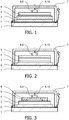
- Elektrolumineszente Vorrichtung, umfassend ein Substrat (1) und in der Reihenfolge ihrer Erwähnung darauf gestapelt eine erste transparente Elektrode (2), einen elektrolumineszenten Stapel (3) und eine zweite Elektrode (4),
wobei die elektrolumineszente Vorrichtung weiter zumindest eine erste zusätzliche Hartschicht, welche sich unterhalb der zweiten Elektrode befindet und aus einer Schicht besteht, welche zumindest ein halbleitendes Metalloxid umfasst, und zumindest eine zweite zusätzliche Hartschicht (5), welche sich oberhalb der zweiten Elektrode befindet, umfasst, und
wobei die erste und die zweite zusätzliche Hartschicht eine Härte aufweisen, welche größer ist als die Härte der zweiten Elektrode, und wobei die zumindest eine zweite zusätzliche Hartschicht eine nichtleitende Schicht ist und zumindest ein Material umfasst, welches ausgewählt ist aus der Gruppe, bestehend aus Oxiden, Nitriden und Fluoriden, und
die elektrolumineszente weiter eine leitende Schicht (6) umfasst, welche sich oberhalb der Hartschicht befindet, welche die zweite Elektrode elektrisch kontaktiert. - Elektrolumineszente Vorrichtung nach Anspruch 1, wobei die zumindest eine zweite zusätzliche Hartschicht sich direkt oberhalb der zweiten Elektrode befindet.
- Elektrolumineszente Vorrichtung nach Anspruch 1, wobei die Dicke der zumindest einen ersten oder zweiten zusätzlichen Hartschicht ≥ 5 nm und ≤ 50 µm ist.
- Elektrolumineszente Vorrichtung nach Anspruch 1, weiter Abdeckungsmittel (7) und zumindest ein Kontaktmittel (8) umfassend, welche angeordnet sind, um direkt oder indirekt die zweite Elektrode elektrisch zu kontaktieren.
- Elektrolumineszente Vorrichtung nach Anspruch 4, wobei das zumindest eine Kontaktmittel ausgewählt ist aus der Gruppe, bestehend aus leitendem Klebstoff (9), einem mechanischen Kontaktmittel (10), einer leitenden Feder, einer leitenden Stütze und einem leitenden Abstandhalter.
- Elektrolumineszente Vorrichtung nach Anspruch 4, weiter ein Gettermaterial umfassend.
- Lichtquelle, Lampe, Monitor, Schalter oder Anzeige, umfassend die elektrolumineszente Vorrichtung nach Anspruch 1.
- Erzeugungsverfahren für eine elektrolumineszente Vorrichtung nach Anspruch 1-6, die folgenden Schritte umfassend:a) Bereitstellen eines Substrats (1); undb) Aufbringen auf dem Substrat in der Reihenfolge ihrer Erwähnung: eine erste transparente Elektrode (2), einen elektrolumineszenten Stapel (3) und eine zweite Elektrode (4),wobei zumindest eine erste zusätzliche Hartschicht, welche aus einer Schicht besteht, welche zumindest ein halbleitendes Metalloxid umfasst, vor dem Aufbringen der zweiten Elektrode aufgebracht wird, und zumindest eine zweite zusätzliche Hartschicht (5) weiter nach dem Aufbringen der zweiten Elektrode aufgebracht wird, und
wobei die erste und die zweite zusätzliche Hartschicht eine Härte aufweisen, welche größer ist als die Härte der zweiten Elektrode, und wobei die zumindest eine zweite zusätzliche Hartschicht eine nichtleitende Schicht ist und zumindest ein Material umfasst, welches ausgewählt ist aus der Gruppe, bestehend aus Oxiden, Nitriden und Fluoriden, und
wobei eine leitende Schicht (6) oberhalb der Hartschicht aufgebracht wird, welche die zweite Elektrode elektrisch kontaktiert. - Verfahren nach Anspruch 8, weiter den Schritt des c) vorübergehenden Kontaktierens der EL-Vorrichtung mit einer Sonde umfassend, um die ordnungsgemäße Funktion der Vorrichtung zu prüfen.
- Verfahren nach Anspruch 8, weiter Anbringen eines Abdeckungsmittels, zumindest eines Kontaktmittels und/oder eines Gettermaterials an der EL-Vorrichtung umfassend.
Priority Applications (1)
| Application Number | Priority Date | Filing Date | Title |
|---|---|---|---|
| EP10796485.0A EP2504873B1 (de) | 2009-11-27 | 2010-11-19 | Verstärkte gegenelektrode elektrolumineszenter vorrichtungen |
Applications Claiming Priority (3)
| Application Number | Priority Date | Filing Date | Title |
|---|---|---|---|
| EP09177352 | 2009-11-27 | ||
| PCT/IB2010/055294 WO2011064700A1 (en) | 2009-11-27 | 2010-11-19 | Strengthened counter electrode of electroluminescent devices |
| EP10796485.0A EP2504873B1 (de) | 2009-11-27 | 2010-11-19 | Verstärkte gegenelektrode elektrolumineszenter vorrichtungen |
Publications (2)
| Publication Number | Publication Date |
|---|---|
| EP2504873A1 EP2504873A1 (de) | 2012-10-03 |
| EP2504873B1 true EP2504873B1 (de) | 2020-01-08 |
Family
ID=43639040
Family Applications (1)
| Application Number | Title | Priority Date | Filing Date |
|---|---|---|---|
| EP10796485.0A Active EP2504873B1 (de) | 2009-11-27 | 2010-11-19 | Verstärkte gegenelektrode elektrolumineszenter vorrichtungen |
Country Status (7)
| Country | Link |
|---|---|
| US (2) | US9425425B2 (de) |
| EP (1) | EP2504873B1 (de) |
| JP (1) | JP5715149B2 (de) |
| KR (1) | KR101858737B1 (de) |
| CN (1) | CN102668161B (de) |
| TW (1) | TW201129247A (de) |
| WO (1) | WO2011064700A1 (de) |
Families Citing this family (2)
| Publication number | Priority date | Publication date | Assignee | Title |
|---|---|---|---|---|
| US9269921B2 (en) * | 2010-10-20 | 2016-02-23 | Semiconductor Energy Laboratory Co., Ltd. | Lighting device |
| KR102202145B1 (ko) * | 2014-03-28 | 2021-01-13 | 삼성디스플레이 주식회사 | 완충패드를 갖는 표시장치 |
Citations (2)
| Publication number | Priority date | Publication date | Assignee | Title |
|---|---|---|---|---|
| JP2003017245A (ja) * | 2001-06-27 | 2003-01-17 | Sony Corp | 有機elディスプレイ及びその駆動回路接続方法 |
| US20050231102A1 (en) * | 2004-04-16 | 2005-10-20 | Chao Ching I | Organic electroluminescence device |
Family Cites Families (21)
| Publication number | Priority date | Publication date | Assignee | Title |
|---|---|---|---|---|
| US6069442A (en) | 1997-09-18 | 2000-05-30 | Eastman Kodak Company | Organic electroluminescent device with inorganic electron transporting layer |
| JP2001052858A (ja) | 1999-08-05 | 2001-02-23 | Futaba Corp | 有機el表示装置 |
| WO2001015244A1 (en) | 1999-08-20 | 2001-03-01 | Emagin Corporation | Organic light emitting diode device with high work function metal-oxide anode layer and method of fabrication of same |
| US6693352B1 (en) * | 2000-06-05 | 2004-02-17 | Emitronix Inc. | Contact structure for group III-V semiconductor devices and method of producing the same |
| JP3773423B2 (ja) | 2001-06-11 | 2006-05-10 | Tdk株式会社 | 有機el素子 |
| TW519853B (en) | 2001-10-17 | 2003-02-01 | Chi Mei Electronic Corp | Organic electro-luminescent display and its packaging method |
| JP4310984B2 (ja) * | 2002-02-06 | 2009-08-12 | 株式会社日立製作所 | 有機発光表示装置 |
| EP1521316B1 (de) | 2003-10-03 | 2016-05-25 | Semiconductor Energy Laboratory Co., Ltd. | Verfahren zur herstellung ein lichtemittierendes Element |
| JP4543691B2 (ja) | 2004-02-03 | 2010-09-15 | 株式会社島津製作所 | 有機エレクトロルミネッセンス素子およびその製造方法 |
| US8241467B2 (en) * | 2004-08-10 | 2012-08-14 | Global Oled Technology Llc | Making a cathode structure for OLEDs |
| JP4329740B2 (ja) * | 2004-10-22 | 2009-09-09 | セイコーエプソン株式会社 | 有機エレクトロルミネッセンス装置の製造方法、及び有機エレクトロルミネッセンス装置 |
| JP2006210233A (ja) | 2005-01-31 | 2006-08-10 | Optrex Corp | 有機elパネルの点灯検査装置 |
| DE602006016109D1 (de) * | 2005-05-23 | 2010-09-23 | Thomson Licensing | Leuchtschirm zum beleuchten oder anzeigen von bilden elektrode |
| EP1911110A2 (de) * | 2005-07-27 | 2008-04-16 | Philips Intellectual Property & Standards GmbH | Lichtemittierende vorrichtung mit abdichtender integrierter treiberschaltung |
| JP2007095518A (ja) | 2005-09-29 | 2007-04-12 | Toppan Printing Co Ltd | 有機エレクトロルミネッセンス表示装置 |
| US20070164673A1 (en) | 2006-01-18 | 2007-07-19 | Au Optronics Corporation | Organic electro-luminescent display device and method for making same |
| US20070241665A1 (en) * | 2006-04-12 | 2007-10-18 | Matsushita Electric Industrial Co., Ltd. | Organic electroluminescent element, and manufacturing method thereof, as well as display device and exposure apparatus using the same |
| TWI307611B (en) | 2006-06-05 | 2009-03-11 | Au Optronics Corp | Organic electroluminescence device and organic electroluminescence panel using the same |
| US20080100202A1 (en) | 2006-11-01 | 2008-05-01 | Cok Ronald S | Process for forming oled conductive protective layer |
| KR100875099B1 (ko) | 2007-06-05 | 2008-12-19 | 삼성모바일디스플레이주식회사 | 유기 발광 장치 및 이의 제조 방법 |
| US8227978B2 (en) | 2007-10-10 | 2012-07-24 | Samsung Electronics Co., Ltd. | White organic light emitting device and color display apparatus employing the same |
-
2010
- 2010-11-19 US US13/509,929 patent/US9425425B2/en active Active
- 2010-11-19 JP JP2012540522A patent/JP5715149B2/ja active Active
- 2010-11-19 EP EP10796485.0A patent/EP2504873B1/de active Active
- 2010-11-19 WO PCT/IB2010/055294 patent/WO2011064700A1/en active Application Filing
- 2010-11-19 KR KR1020127016606A patent/KR101858737B1/ko active IP Right Grant
- 2010-11-19 CN CN201080053540.6A patent/CN102668161B/zh active Active
- 2010-11-24 TW TW099140624A patent/TW201129247A/zh unknown
-
2016
- 2016-07-25 US US15/218,410 patent/US20160336535A1/en not_active Abandoned
Patent Citations (2)
| Publication number | Priority date | Publication date | Assignee | Title |
|---|---|---|---|---|
| JP2003017245A (ja) * | 2001-06-27 | 2003-01-17 | Sony Corp | 有機elディスプレイ及びその駆動回路接続方法 |
| US20050231102A1 (en) * | 2004-04-16 | 2005-10-20 | Chao Ching I | Organic electroluminescence device |
Also Published As
| Publication number | Publication date |
|---|---|
| JP5715149B2 (ja) | 2015-05-07 |
| WO2011064700A1 (en) | 2011-06-03 |
| US20160336535A1 (en) | 2016-11-17 |
| JP2013512542A (ja) | 2013-04-11 |
| CN102668161A (zh) | 2012-09-12 |
| KR101858737B1 (ko) | 2018-05-18 |
| KR20120113742A (ko) | 2012-10-15 |
| US9425425B2 (en) | 2016-08-23 |
| US20120228667A1 (en) | 2012-09-13 |
| TW201129247A (en) | 2011-08-16 |
| EP2504873A1 (de) | 2012-10-03 |
| CN102668161B (zh) | 2015-12-09 |
Similar Documents
| Publication | Publication Date | Title |
|---|---|---|
| US6548961B2 (en) | Organic light emitting devices | |
| US8963143B2 (en) | Organic electroluminescent device | |
| EP2460205B1 (de) | Verkapseltes optoelektronisches bauelement und herstellungsverfahren dafür | |
| US7321196B2 (en) | Organic light emitting diode with transparent electrode structure having dielectric layer | |
| JP2007536697A (ja) | フレキシブルエレクトロルミネッセンスデバイス | |
| US8508122B2 (en) | Organic electroluminescent device | |
| GB2348316A (en) | Organic opto-electronic device | |
| KR101695004B1 (ko) | 전계 발광 장치 | |
| US8847258B2 (en) | Organic electroluminescent devices | |
| KR20120027313A (ko) | 전계 발광 소자 | |
| US20160336535A1 (en) | Strengthened counter electrode of electroluminescent devices | |
| KR100552965B1 (ko) | 유기 전계 발광 표시 장치 | |
| US8610115B2 (en) | Organic electroluminescent devices | |
| JP5714003B2 (ja) | エレクトロルミネッセンス装置 | |
| KR20080104324A (ko) | 가요성 전기발광 소자 | |
| WO2010136963A1 (en) | Electroluminescent devices | |
| Hao et al. | Top emitting poly (p-phenylene vinylene) light-emitting diodes on metal sandwiched polyethylene terephthalate substrates | |
| WO2010089684A1 (en) | Electroluminescent device | |
| KR20060111643A (ko) | 가요성 전기발광 소자 |
Legal Events
| Date | Code | Title | Description |
|---|---|---|---|
| PUAI | Public reference made under article 153(3) epc to a published international application that has entered the european phase |
Free format text: ORIGINAL CODE: 0009012 |
|
| 17P | Request for examination filed |
Effective date: 20120627 |
|
| AK | Designated contracting states |
Kind code of ref document: A1 Designated state(s): AL AT BE BG CH CY CZ DE DK EE ES FI FR GB GR HR HU IE IS IT LI LT LU LV MC MK MT NL NO PL PT RO RS SE SI SK SM TR |
|
| DAX | Request for extension of the european patent (deleted) | ||
| RAP1 | Party data changed (applicant data changed or rights of an application transferred) |
Owner name: KONINKLIJKE PHILIPS N.V. Owner name: PHILIPS INTELLECTUAL PROPERTY & STANDARDS GMBH |
|
| STAA | Information on the status of an ep patent application or granted ep patent |
Free format text: STATUS: EXAMINATION IS IN PROGRESS |
|
| 17Q | First examination report despatched |
Effective date: 20170228 |
|
| GRAP | Despatch of communication of intention to grant a patent |
Free format text: ORIGINAL CODE: EPIDOSNIGR1 |
|
| STAA | Information on the status of an ep patent application or granted ep patent |
Free format text: STATUS: GRANT OF PATENT IS INTENDED |
|
| INTG | Intention to grant announced |
Effective date: 20190802 |
|
| GRAS | Grant fee paid |
Free format text: ORIGINAL CODE: EPIDOSNIGR3 |
|
| GRAA | (expected) grant |
Free format text: ORIGINAL CODE: 0009210 |
|
| STAA | Information on the status of an ep patent application or granted ep patent |
Free format text: STATUS: THE PATENT HAS BEEN GRANTED |
|
| AK | Designated contracting states |
Kind code of ref document: B1 Designated state(s): AL AT BE BG CH CY CZ DE DK EE ES FI FR GB GR HR HU IE IS IT LI LT LU LV MC MK MT NL NO PL PT RO RS SE SI SK SM TR |
|
| REG | Reference to a national code |
Ref country code: GB Ref legal event code: FG4D |
|
| REG | Reference to a national code |
Ref country code: CH Ref legal event code: EP |
|
| REG | Reference to a national code |
Ref country code: DE Ref legal event code: R096 Ref document number: 602010062736 Country of ref document: DE |
|
| REG | Reference to a national code |
Ref country code: IE Ref legal event code: FG4D |
|
| REG | Reference to a national code |
Ref country code: AT Ref legal event code: REF Ref document number: 1223794 Country of ref document: AT Kind code of ref document: T Effective date: 20200215 |
|
| RAP2 | Party data changed (patent owner data changed or rights of a patent transferred) |
Owner name: PHILIPS INTELLECTUAL PROPERTY & STANDARDS GMBH Owner name: KONINKLIJKE PHILIPS N.V. |
|
| REG | Reference to a national code |
Ref country code: NL Ref legal event code: MP Effective date: 20200108 |
|
| REG | Reference to a national code |
Ref country code: LT Ref legal event code: MG4D |
|
| PG25 | Lapsed in a contracting state [announced via postgrant information from national office to epo] |
Ref country code: PT Free format text: LAPSE BECAUSE OF FAILURE TO SUBMIT A TRANSLATION OF THE DESCRIPTION OR TO PAY THE FEE WITHIN THE PRESCRIBED TIME-LIMIT Effective date: 20200531 Ref country code: RS Free format text: LAPSE BECAUSE OF FAILURE TO SUBMIT A TRANSLATION OF THE DESCRIPTION OR TO PAY THE FEE WITHIN THE PRESCRIBED TIME-LIMIT Effective date: 20200108 Ref country code: FI Free format text: LAPSE BECAUSE OF FAILURE TO SUBMIT A TRANSLATION OF THE DESCRIPTION OR TO PAY THE FEE WITHIN THE PRESCRIBED TIME-LIMIT Effective date: 20200108 Ref country code: NO Free format text: LAPSE BECAUSE OF FAILURE TO SUBMIT A TRANSLATION OF THE DESCRIPTION OR TO PAY THE FEE WITHIN THE PRESCRIBED TIME-LIMIT Effective date: 20200408 Ref country code: NL Free format text: LAPSE BECAUSE OF FAILURE TO SUBMIT A TRANSLATION OF THE DESCRIPTION OR TO PAY THE FEE WITHIN THE PRESCRIBED TIME-LIMIT Effective date: 20200108 Ref country code: LT Free format text: LAPSE BECAUSE OF FAILURE TO SUBMIT A TRANSLATION OF THE DESCRIPTION OR TO PAY THE FEE WITHIN THE PRESCRIBED TIME-LIMIT Effective date: 20200108 |
|
| PG25 | Lapsed in a contracting state [announced via postgrant information from national office to epo] |
Ref country code: IS Free format text: LAPSE BECAUSE OF FAILURE TO SUBMIT A TRANSLATION OF THE DESCRIPTION OR TO PAY THE FEE WITHIN THE PRESCRIBED TIME-LIMIT Effective date: 20200508 Ref country code: BG Free format text: LAPSE BECAUSE OF FAILURE TO SUBMIT A TRANSLATION OF THE DESCRIPTION OR TO PAY THE FEE WITHIN THE PRESCRIBED TIME-LIMIT Effective date: 20200408 Ref country code: HR Free format text: LAPSE BECAUSE OF FAILURE TO SUBMIT A TRANSLATION OF THE DESCRIPTION OR TO PAY THE FEE WITHIN THE PRESCRIBED TIME-LIMIT Effective date: 20200108 Ref country code: GR Free format text: LAPSE BECAUSE OF FAILURE TO SUBMIT A TRANSLATION OF THE DESCRIPTION OR TO PAY THE FEE WITHIN THE PRESCRIBED TIME-LIMIT Effective date: 20200409 Ref country code: SE Free format text: LAPSE BECAUSE OF FAILURE TO SUBMIT A TRANSLATION OF THE DESCRIPTION OR TO PAY THE FEE WITHIN THE PRESCRIBED TIME-LIMIT Effective date: 20200108 Ref country code: LV Free format text: LAPSE BECAUSE OF FAILURE TO SUBMIT A TRANSLATION OF THE DESCRIPTION OR TO PAY THE FEE WITHIN THE PRESCRIBED TIME-LIMIT Effective date: 20200108 |
|
| REG | Reference to a national code |
Ref country code: DE Ref legal event code: R097 Ref document number: 602010062736 Country of ref document: DE |
|
| PG25 | Lapsed in a contracting state [announced via postgrant information from national office to epo] |
Ref country code: EE Free format text: LAPSE BECAUSE OF FAILURE TO SUBMIT A TRANSLATION OF THE DESCRIPTION OR TO PAY THE FEE WITHIN THE PRESCRIBED TIME-LIMIT Effective date: 20200108 Ref country code: SM Free format text: LAPSE BECAUSE OF FAILURE TO SUBMIT A TRANSLATION OF THE DESCRIPTION OR TO PAY THE FEE WITHIN THE PRESCRIBED TIME-LIMIT Effective date: 20200108 Ref country code: DK Free format text: LAPSE BECAUSE OF FAILURE TO SUBMIT A TRANSLATION OF THE DESCRIPTION OR TO PAY THE FEE WITHIN THE PRESCRIBED TIME-LIMIT Effective date: 20200108 Ref country code: SK Free format text: LAPSE BECAUSE OF FAILURE TO SUBMIT A TRANSLATION OF THE DESCRIPTION OR TO PAY THE FEE WITHIN THE PRESCRIBED TIME-LIMIT Effective date: 20200108 Ref country code: CZ Free format text: LAPSE BECAUSE OF FAILURE TO SUBMIT A TRANSLATION OF THE DESCRIPTION OR TO PAY THE FEE WITHIN THE PRESCRIBED TIME-LIMIT Effective date: 20200108 Ref country code: ES Free format text: LAPSE BECAUSE OF FAILURE TO SUBMIT A TRANSLATION OF THE DESCRIPTION OR TO PAY THE FEE WITHIN THE PRESCRIBED TIME-LIMIT Effective date: 20200108 Ref country code: RO Free format text: LAPSE BECAUSE OF FAILURE TO SUBMIT A TRANSLATION OF THE DESCRIPTION OR TO PAY THE FEE WITHIN THE PRESCRIBED TIME-LIMIT Effective date: 20200108 |
|
| PLBE | No opposition filed within time limit |
Free format text: ORIGINAL CODE: 0009261 |
|
| STAA | Information on the status of an ep patent application or granted ep patent |
Free format text: STATUS: NO OPPOSITION FILED WITHIN TIME LIMIT |
|
| REG | Reference to a national code |
Ref country code: AT Ref legal event code: MK05 Ref document number: 1223794 Country of ref document: AT Kind code of ref document: T Effective date: 20200108 |
|
| 26N | No opposition filed |
Effective date: 20201009 |
|
| REG | Reference to a national code |
Ref country code: DE Ref legal event code: R081 Ref document number: 602010062736 Country of ref document: DE Owner name: PHILIPS GMBH, DE Free format text: FORMER OWNER: PHILIPS INTELLECTUAL PROPERTY & STANDARDS GMBH, 20099 HAMBURG, DE |
|
| PG25 | Lapsed in a contracting state [announced via postgrant information from national office to epo] |
Ref country code: IT Free format text: LAPSE BECAUSE OF FAILURE TO SUBMIT A TRANSLATION OF THE DESCRIPTION OR TO PAY THE FEE WITHIN THE PRESCRIBED TIME-LIMIT Effective date: 20200108 Ref country code: AT Free format text: LAPSE BECAUSE OF FAILURE TO SUBMIT A TRANSLATION OF THE DESCRIPTION OR TO PAY THE FEE WITHIN THE PRESCRIBED TIME-LIMIT Effective date: 20200108 |
|
| PG25 | Lapsed in a contracting state [announced via postgrant information from national office to epo] |
Ref country code: SI Free format text: LAPSE BECAUSE OF FAILURE TO SUBMIT A TRANSLATION OF THE DESCRIPTION OR TO PAY THE FEE WITHIN THE PRESCRIBED TIME-LIMIT Effective date: 20200108 Ref country code: PL Free format text: LAPSE BECAUSE OF FAILURE TO SUBMIT A TRANSLATION OF THE DESCRIPTION OR TO PAY THE FEE WITHIN THE PRESCRIBED TIME-LIMIT Effective date: 20200108 |
|
| PG25 | Lapsed in a contracting state [announced via postgrant information from national office to epo] |
Ref country code: MC Free format text: LAPSE BECAUSE OF FAILURE TO SUBMIT A TRANSLATION OF THE DESCRIPTION OR TO PAY THE FEE WITHIN THE PRESCRIBED TIME-LIMIT Effective date: 20200108 |
|
| REG | Reference to a national code |
Ref country code: CH Ref legal event code: PL |
|
| PG25 | Lapsed in a contracting state [announced via postgrant information from national office to epo] |
Ref country code: LU Free format text: LAPSE BECAUSE OF NON-PAYMENT OF DUE FEES Effective date: 20201119 |
|
| REG | Reference to a national code |
Ref country code: BE Ref legal event code: MM Effective date: 20201130 |
|
| PG25 | Lapsed in a contracting state [announced via postgrant information from national office to epo] |
Ref country code: CH Free format text: LAPSE BECAUSE OF NON-PAYMENT OF DUE FEES Effective date: 20201130 Ref country code: LI Free format text: LAPSE BECAUSE OF NON-PAYMENT OF DUE FEES Effective date: 20201130 |
|
| PG25 | Lapsed in a contracting state [announced via postgrant information from national office to epo] |
Ref country code: IE Free format text: LAPSE BECAUSE OF NON-PAYMENT OF DUE FEES Effective date: 20201119 |
|
| PG25 | Lapsed in a contracting state [announced via postgrant information from national office to epo] |
Ref country code: TR Free format text: LAPSE BECAUSE OF FAILURE TO SUBMIT A TRANSLATION OF THE DESCRIPTION OR TO PAY THE FEE WITHIN THE PRESCRIBED TIME-LIMIT Effective date: 20200108 Ref country code: MT Free format text: LAPSE BECAUSE OF FAILURE TO SUBMIT A TRANSLATION OF THE DESCRIPTION OR TO PAY THE FEE WITHIN THE PRESCRIBED TIME-LIMIT Effective date: 20200108 Ref country code: CY Free format text: LAPSE BECAUSE OF FAILURE TO SUBMIT A TRANSLATION OF THE DESCRIPTION OR TO PAY THE FEE WITHIN THE PRESCRIBED TIME-LIMIT Effective date: 20200108 |
|
| PG25 | Lapsed in a contracting state [announced via postgrant information from national office to epo] |
Ref country code: MK Free format text: LAPSE BECAUSE OF FAILURE TO SUBMIT A TRANSLATION OF THE DESCRIPTION OR TO PAY THE FEE WITHIN THE PRESCRIBED TIME-LIMIT Effective date: 20200108 Ref country code: AL Free format text: LAPSE BECAUSE OF FAILURE TO SUBMIT A TRANSLATION OF THE DESCRIPTION OR TO PAY THE FEE WITHIN THE PRESCRIBED TIME-LIMIT Effective date: 20200108 |
|
| PG25 | Lapsed in a contracting state [announced via postgrant information from national office to epo] |
Ref country code: BE Free format text: LAPSE BECAUSE OF NON-PAYMENT OF DUE FEES Effective date: 20201130 |
|
| REG | Reference to a national code |
Ref country code: DE Ref legal event code: R079 Ref document number: 602010062736 Country of ref document: DE Free format text: PREVIOUS MAIN CLASS: H01L0051520000 Ipc: H10K0050800000 |
|
| PGFP | Annual fee paid to national office [announced via postgrant information from national office to epo] |
Ref country code: GB Payment date: 20231121 Year of fee payment: 14 |
|
| PGFP | Annual fee paid to national office [announced via postgrant information from national office to epo] |
Ref country code: FR Payment date: 20231123 Year of fee payment: 14 Ref country code: DE Payment date: 20231127 Year of fee payment: 14 |