EP2503556B1 - Memristives System - Google Patents
Memristives System Download PDFInfo
- Publication number
- EP2503556B1 EP2503556B1 EP12161274.1A EP12161274A EP2503556B1 EP 2503556 B1 EP2503556 B1 EP 2503556B1 EP 12161274 A EP12161274 A EP 12161274A EP 2503556 B1 EP2503556 B1 EP 2503556B1
- Authority
- EP
- European Patent Office
- Prior art keywords
- memristive
- coil
- current
- hall
- effect
- Prior art date
- Legal status (The legal status is an assumption and is not a legal conclusion. Google has not performed a legal analysis and makes no representation as to the accuracy of the status listed.)
- Not-in-force
Links
Images

Classifications
-
- G—PHYSICS
- G01—MEASURING; TESTING
- G01R—MEASURING ELECTRIC VARIABLES; MEASURING MAGNETIC VARIABLES
- G01R33/00—Arrangements or instruments for measuring magnetic variables
- G01R33/0023—Electronic aspects, e.g. circuits for stimulation, evaluation, control; Treating the measured signals; calibration
- G01R33/0041—Electronic aspects, e.g. circuits for stimulation, evaluation, control; Treating the measured signals; calibration using feed-back or modulation techniques
-
- G—PHYSICS
- G06—COMPUTING OR CALCULATING; COUNTING
- G06N—COMPUTING ARRANGEMENTS BASED ON SPECIFIC COMPUTATIONAL MODELS
- G06N3/00—Computing arrangements based on biological models
- G06N3/02—Neural networks
- G06N3/06—Physical realisation, i.e. hardware implementation of neural networks, neurons or parts of neurons
- G06N3/063—Physical realisation, i.e. hardware implementation of neural networks, neurons or parts of neurons using electronic means
- G06N3/065—Analogue means
-
- G—PHYSICS
- G11—INFORMATION STORAGE
- G11C—STATIC STORES
- G11C11/00—Digital stores characterised by the use of particular electric or magnetic storage elements; Storage elements therefor
- G11C11/02—Digital stores characterised by the use of particular electric or magnetic storage elements; Storage elements therefor using magnetic elements
- G11C11/16—Digital stores characterised by the use of particular electric or magnetic storage elements; Storage elements therefor using magnetic elements using elements in which the storage effect is based on magnetic spin effect
- G11C11/161—Digital stores characterised by the use of particular electric or magnetic storage elements; Storage elements therefor using magnetic elements using elements in which the storage effect is based on magnetic spin effect details concerning the memory cell structure, e.g. the layers of the ferromagnetic memory cell
-
- G—PHYSICS
- G11—INFORMATION STORAGE
- G11C—STATIC STORES
- G11C11/00—Digital stores characterised by the use of particular electric or magnetic storage elements; Storage elements therefor
- G11C11/18—Digital stores characterised by the use of particular electric or magnetic storage elements; Storage elements therefor using Hall-effect devices
-
- G—PHYSICS
- G11—INFORMATION STORAGE
- G11C—STATIC STORES
- G11C11/00—Digital stores characterised by the use of particular electric or magnetic storage elements; Storage elements therefor
- G11C11/54—Digital stores characterised by the use of particular electric or magnetic storage elements; Storage elements therefor using elements simulating biological cells, e.g. neuron
-
- G—PHYSICS
- G11—INFORMATION STORAGE
- G11C—STATIC STORES
- G11C11/00—Digital stores characterised by the use of particular electric or magnetic storage elements; Storage elements therefor
- G11C11/56—Digital stores characterised by the use of particular electric or magnetic storage elements; Storage elements therefor using storage elements with more than two stable states represented by steps, e.g. of voltage, current, phase, frequency
- G11C11/5685—Digital stores characterised by the use of particular electric or magnetic storage elements; Storage elements therefor using storage elements with more than two stable states represented by steps, e.g. of voltage, current, phase, frequency using storage elements comprising metal oxide memory material, e.g. perovskites
-
- G—PHYSICS
- G11—INFORMATION STORAGE
- G11C—STATIC STORES
- G11C13/00—Digital stores characterised by the use of storage elements not covered by groups G11C11/00, G11C23/00, or G11C25/00
- G11C13/0002—Digital stores characterised by the use of storage elements not covered by groups G11C11/00, G11C23/00, or G11C25/00 using resistive RAM [RRAM] elements
- G11C13/0007—Digital stores characterised by the use of storage elements not covered by groups G11C11/00, G11C23/00, or G11C25/00 using resistive RAM [RRAM] elements comprising metal oxide memory material, e.g. perovskites
-
- G—PHYSICS
- G11—INFORMATION STORAGE
- G11C—STATIC STORES
- G11C27/00—Electric analogue stores, e.g. for storing instantaneous values
- G11C27/005—Electric analogue stores, e.g. for storing instantaneous values with non-volatile charge storage, e.g. on floating gate or MNOS
-
- H—ELECTRICITY
- H01—ELECTRIC ELEMENTS
- H01F—MAGNETS; INDUCTANCES; TRANSFORMERS; SELECTION OF MATERIALS FOR THEIR MAGNETIC PROPERTIES
- H01F10/00—Thin magnetic films, e.g. of one-domain structure
- H01F10/32—Spin-exchange-coupled multilayers, e.g. nanostructured superlattices
- H01F10/324—Exchange coupling of magnetic film pairs via a very thin non-magnetic spacer, e.g. by exchange with conduction electrons of the spacer
- H01F10/325—Exchange coupling of magnetic film pairs via a very thin non-magnetic spacer, e.g. by exchange with conduction electrons of the spacer the spacer being noble metal
-
- H—ELECTRICITY
- H03—ELECTRONIC CIRCUITRY
- H03B—GENERATION OF OSCILLATIONS, DIRECTLY OR BY FREQUENCY-CHANGING, BY CIRCUITS EMPLOYING ACTIVE ELEMENTS WHICH OPERATE IN A NON-SWITCHING MANNER; GENERATION OF NOISE BY SUCH CIRCUITS
- H03B15/00—Generation of oscillations using galvano-magnetic devices, e.g. Hall-effect devices, or using superconductivity effects
- H03B15/006—Generation of oscillations using galvano-magnetic devices, e.g. Hall-effect devices, or using superconductivity effects using spin transfer effects or giant magnetoresistance
-
- H—ELECTRICITY
- H01—ELECTRIC ELEMENTS
- H01F—MAGNETS; INDUCTANCES; TRANSFORMERS; SELECTION OF MATERIALS FOR THEIR MAGNETIC PROPERTIES
- H01F10/00—Thin magnetic films, e.g. of one-domain structure
- H01F10/32—Spin-exchange-coupled multilayers, e.g. nanostructured superlattices
- H01F10/324—Exchange coupling of magnetic film pairs via a very thin non-magnetic spacer, e.g. by exchange with conduction electrons of the spacer
- H01F10/329—Spin-exchange coupled multilayers wherein the magnetisation of the free layer is switched by a spin-polarised current, e.g. spin torque effect
Definitions
- the present invention relates to a memristive system and a method to induce a memristive effect.
- memristors Commercial applications include oscillators and controllers.
- the memristor is a typical element which can be used to implement nonlinear circuits, including memristor-based oscillators, chaotic circuits. Furthermore, the memristor can be used to construct a control loop.
- Fig. 4 shows the two-memristive oscillator network.
- Fig. 5 shows in-phase (a) and anti-phase (b) behaviors of the oscillator network shown in Fig. 4 .
- Fig. 6 shows the canonical Chua's oscillator with memristor.
- Fig. 7 shows a chaotic attractor of the oscillator shown in Fig.6 .
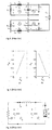
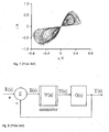
- Nanotechnology Materials and Devices Conference Oct 12 - 15, 2010, Monterey, California, USA relates to a possible control loop comprising a memristor as a controller as shown in Fig. 8 .
- An error signal E(s) is the difference between reference signal R(s) and measured system output Y(s).
- the error signal is fed to the controller which is a memristor in this case.
- the controller changes the inputs U(s) of a system under control of G(s).
- the system output Y(s) is fed back.
- the memristive system principally comprises means for generating a spin polarization process and means for generating a memory effect in the voltage-current phase plane, in a way that these means are arranged in a feedback loop architecture, such that the feedback loop is established by combining the spin polarization process with the action of a classical Hall effect, wherein a Hall current is fed back by transforming the Hall current to a magnetic flux.
- a memristive effect is induced by establishing a feedback loop process that combines a spin polarization process with the action of the classical Hall effect.
- the feedback loop architecture of the proposed memristive system comprises a giant magnetoresistive (GMR) material and a coil.
- the feedback loop controls the spin polarization in a giant magnetoresistive material via the classical Hall Effect, which gives rise to a memory behaviour.
- the giant magnetoresistive (GMR) material contains a stacked thin-film material formed as a spin-valve device. That is, it consists of two or more conducting materials. At least one of these materials, the "ferromagnetic material”, may be strongly influenced if a magnetic field is applied to it in a way that it is strongly polarized by the magnetic field. This means results in a spin-alignment within this material. At least one other of the above mentioned conducting materials, the "non-ferromagnetic material”, either does not show at all or shows only a polarization effect at a very low, insignificant level while applying the same magnetic field to it.
- the so formed spin-valve device alternates its electrical resistance depending on the level of spin-alignment within the ferromagnetic material. This allows the exploit the so-called Giant Magnetoresistive effect while placing a stack of layers of these materials in an alterable magnetic field.
- this advantageous embodiment represents a spin-valve memristive system established on a feedback loop.
- the above mentioned stacked thin-film material is realized by a periodic succession of a ferromagnetic layer and a non-ferromagnetic layer. While applying a magnetic field, the ferromagnetic layer will be spin-polarized while roughly no effect will be seen within the non-ferromagnetic layer.
- the thin film material is arranged in a current-perpendicular-to-plane (CPP) configuration. That is, an external voltage u resulting in an external current i is applied perpendicularly to the mentioned layers of the GMR material. In other words, the current direction is parallel to the stack direction.
- CPP current-perpendicular-to-plane
- the parallel spin alignment corresponds to a low resistance R ⁇ and the anti-parallel spin alignment corresponds to a high resistance R ⁇ .
- ⁇ m0 denotes a normalization quantity with the dimension of magnetic flux.
- the classical Hall Effect is employed to feed back a magnetic field as a control of the spin polarization in the ferromagnetic layers of the GMR material.
- the classical Hall Effect is based on a balance between the Lorenz force and the established inner electric field.
- an "external" current i is caused by an external voltage u on a magnetoresistive conductor, a magnetic field B is supplied internally by the Hall current iH, the Hall current is drawn out to a coil by the Hall electromotive force and the drawn out Hall current feeds back a controlling magnetic flux ⁇ m on the magnetoresistive conductor.
- the magnetic field B is supplied internally by the Hall current i H .
- the Hall current is drawn by the Hall electromotive force out to a coil, feeding back a controlling magnetic flux ⁇ m the conductor itself, the balance is sustained in a dynamic way.
- the inductance L increases to a large extent with the enhanced permeability (by a factor of several hundred to thousand) and the dimension of the coil is allowed to be larger than that of the core due to the magnetic flux confinement.
- the coil resistance RL is constant.
- this resistance also includes a transverse resistance of the ferromagnetic conductor.
- the transverse resistance is relatively small (by properly choosing the size ratio of the GMR material) and its temporal change is negligible in series with the main coil resistance, and hence R L is regarded constant.
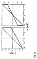
- the system is first characterized by starting with a distinct set of parameters and then altering the inductance of the coil L and/or the frequency f of the alternating external voltage signal into a distinct direction, either to increased or to decreased values, while the alteration of the resulting hysteretic loop is observed.
- a "single hystereric loop" is generated by applying a low inductance of the coil L and/or the a low frequency f of the alternating external voltage signal and a "pinched hysteretic loop” is generated by applying a high inductance of the coil L and/or a high frequency of the alternating external voltage signal.
- the single hysteric loop does not show the normally observed pinching effect with a self crossing point as of for pinched hysteric loops (the so-called "bi-loop”). Thus it is a new type of memristive dynamics.
- the memristive system of this invention comprises a completely new device architecture as well as the method of inducing a memristing effect of this invention comprises a completely new technique. They are based on three formerly independent elements and effects: the general concept of memristor and memristive systems, the use of giant magnetoresistive (GMR) material and the application of the classical Hall Effect.
- GMR giant magnetoresistive
- the above described memristive system as well as the method of inducing a memristive effect according to the invention as well as to special aspects of the invention may be applied within neuromorphic systems and/or programmable analog signals and/or stateful logic circuits and/or low resistive range (e.g. conductor) applications, filling upto now existing gaps in these domains, opening the way to widely sought applications of these domains.
- programmable analog signals and/or stateful logic circuits and/or low resistive range e.g. conductor
- the memristive system according to the present invention exhibits a small memristance at the ohmic range. Therefore, it can be used as a compensating element for devices processing high memristance, for example, the one proposed by the HP laboratory.
- the potential applications of the memristive system are, but not exclusively, nonlinear circuits and control loops. Specifically, the memristive according to the present invention may be used in a control loop in which a low memristance is required.
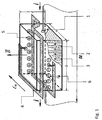
- the fig. 1 proposes a memresistive system built up by a giant magnetoresistive material, containing a stacked thin film material 1 formed as spin-valve device in a current perpendicular-to-plane (CPP) configuration.
- the thin film stack is a realized by a periodic succession of a ferromagnetic layer 3 and a non-ferromagnetic layer 2.
- this stack can be obtained by a periodic succession of a Fe-layer of a thickness between 1 and 2nm and a Cr-layer of a thickness of about 3nm. Without limiting to it, the total thickness of the stack might be in the order of micrometers.
- a coil 4 is created winded around the giant magnetoresistive material 1 as shown in fig. 1 , contacting the giant magnetoresistive material 1 in the planes perpendicular to the layers as shown in fig. 1 .
- the coil 4 may beentred by the Hall current i H , drawn out to the coil 4 by the Hall electromotive force ⁇ H and feeding back a controlling magnetic flux ⁇ m on the conductor, e.g. the stacked thin film giant magnetoresistive material 1 itself, once the system is in operation.
- An alternating external voltage u is applied parallel to the stack direction of the stacked thin film giant magnetoresistive material 1, leading to a current i through this material.
- the spin in the ferromagnetic layers 3 are polarized adaptively to the temporally changing magnetic flux induced by the Hall current, while those in the non-ferromagnetic layers 2 are averaged to zero.
- the current-perpendicular-to-plane (CPP) configuration of the thin-film stack is to adopt, to yield to the highest giant magnetoresistance along the external current i, which possesses a GMR coefficient ⁇ (R ⁇ - R ⁇ ) / R ⁇ that can exceed 1.
- u(t) u 0 cos( ⁇ t)
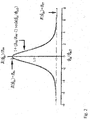
- the trajectory crosses the origin only once in each period in case of the conditions chosen for fig. 3a , simply attributed to the additional non-zero term to the resistive relation in equation (5a).
- the u - i planar dynamics exhibits this single hysteretic loop (i.e. non-pinched orbit), which is a new type of memristive dynamics, while in case of the conditions chosen for fig. 3b , it also exhibits a memristive hysteretic pinch, having its self-crossing point almost located at the origin as in a standard memristor.
- Hard switching resposes under a square-wave input voltage signal demonstrates more clearly the two distinct topologies, as shown in fig. 3c .
- Globally, the two u - i orbits are topologically homeomorphic to the Lissajous figures for the ratio of 1 and 2, respectively.
Landscapes
- Engineering & Computer Science (AREA)
- Physics & Mathematics (AREA)
- Computer Hardware Design (AREA)
- Health & Medical Sciences (AREA)
- Life Sciences & Earth Sciences (AREA)
- Biomedical Technology (AREA)
- Chemical & Material Sciences (AREA)
- Molecular Biology (AREA)
- General Physics & Mathematics (AREA)
- Materials Engineering (AREA)
- Biophysics (AREA)
- General Health & Medical Sciences (AREA)
- Neurology (AREA)
- Theoretical Computer Science (AREA)
- Artificial Intelligence (AREA)
- General Engineering & Computer Science (AREA)
- Mathematical Physics (AREA)
- Software Systems (AREA)
- Computing Systems (AREA)
- Condensed Matter Physics & Semiconductors (AREA)
- Computational Linguistics (AREA)
- Evolutionary Computation (AREA)
- Data Mining & Analysis (AREA)
- Crystallography & Structural Chemistry (AREA)
- Power Engineering (AREA)
- Hall/Mr Elements (AREA)
Claims (10)
- Memristives System, das Folgendes umfasst:- Mittel zum Erzeugen eines Spin-Polarisierungsvorgangs- Mittel zum Erzeugen eines Speichereffekts in der Spannungs-Strom-Phasenebenedadurch gekennzeichnet, dass- die erwähnten Mittel in einer Rückkopplungsschleifenarchitektur angeordnet sind, derart, dass die Rückkopplungsschleife durch Kombinieren des Spin-Polarisierungsvorgangs mit dem Vorgang eines klassischen Hall-Effekts eingerichtet wird, wobei ein Hall-Strom durch Umwandeln des Hall-Stroms in einen magnetischen Fluss rückgekoppelt wird.
- Memristives System nach Anspruch 1, dadurch gekennzeichnet, dass die Rückkopplungsschleifenarchitektur ein riesenmagnetoresistives Material (GMR-Material) und eine Spule (4) umfasst.
- Memristives System nach Anspruch 2, dadurch gekennzeichnet, dass das riesenmagnetoresistive Material (GMR-Material) ein geschichtetes Dünnschichtmaterial (1) enthält, das als ein Spinventil (eine Spinventil-Vorrichtung) ausgebildet ist.
- Memristives System nach Anspruch 3, dadurch gekennzeichnet, dass das geschichtete Dünnschichtmaterial durch eine periodische Folge einer ferromagnetischen Schicht (3) und einer nicht ferromagnetischen Schicht (2) realisiert wird.
- Memristives System nach den Ansprüchen 3 oder 4, dadurch gekennzeichnet, dass das Dünnschichtmaterial in einer Strom-senkrecht-zur-Ebene-Konfiguration (CPP-Konfiguration) angeordnet ist.
- Verfahren zum Induzieren eines memristiven Effekts, dadurch gekennzeichnet, dass eine Rückkopplungsschleife durch Kombinieren eines Spin-Polarisierungsvorgangs mit dem Vorgang des klassischen Hall-Effekts eingerichtet wird.
- Verfahren nach Anspruch 6, dadurch gekennzeichnet, dass- in einem magnetoresistiven Leiter (1) durch eine externe Spannung (u) ein Strom (i) verursacht wird,- ein Magnetfeld B intern durch den Hall-Strom (iH) bereitgestellt wird,- der Hall-Strom (iH) durch die elektromotorische Hall-Kraft (εH) in eine Spule (4) gezogen wird, und- der gezogene Hall-Strom (iH) einen steuernden Magnetfluss (Φm) auf den magnetoresistiven Leiter (1) rückkoppelt.
- Verfahren nach Anspruch 7, dadurch gekennzeichnet, dass durch Erhöhen oder Erniedrigen der Induktivität (L) der Spule (4) und der Frequenz (f) des externen Wechselspannungssignals (u) mindestens zwei verschiedene Typen von Hystereseschleifen realisiert werden.
- Verfahren nach Anspruch 8, dadurch gekennzeichnet, dass durch Anlegen einer niedrigen Induktivität (L) der Spule (4) und/oder einer niedrigen Frequenz (f) des externen Wechselspannungssignals (u) eine einzelne Hystereseschleife erzeugt wird und dass durch Anlegen einer hohen Induktivität (L) der Spule (4) und/oder einer hohen Frequenz (f) des externen Wechselspannungssignals (u) eine eingeschnürte Hystereseschleife erzeugt wird.
- Verwendung eines memristiven Systems nach einem der Ansprüche 1 bis 5 und/oder eines Verfahrens zum Induzieren eines memristiven Effekts nach einem der Ansprüche 6 bis 9, dadurch gekennzeichnet, dass sie in neuromorphischen Systemen und/oder in programmierbaren, analogen Signalen und/oder in zustandsorientierten logischen Schaltungen und/oder in Anwendungen im niederohmigen Bereich angewendet werden.
Priority Applications (1)
| Application Number | Priority Date | Filing Date | Title |
|---|---|---|---|
| EP12161274.1A EP2503556B1 (de) | 2011-03-25 | 2012-03-26 | Memristives System |
Applications Claiming Priority (2)
| Application Number | Priority Date | Filing Date | Title |
|---|---|---|---|
| EP11159905 | 2011-03-25 | ||
| EP12161274.1A EP2503556B1 (de) | 2011-03-25 | 2012-03-26 | Memristives System |
Publications (2)
| Publication Number | Publication Date |
|---|---|
| EP2503556A1 EP2503556A1 (de) | 2012-09-26 |
| EP2503556B1 true EP2503556B1 (de) | 2016-10-12 |
Family
ID=46026622
Family Applications (1)
| Application Number | Title | Priority Date | Filing Date |
|---|---|---|---|
| EP12161274.1A Not-in-force EP2503556B1 (de) | 2011-03-25 | 2012-03-26 | Memristives System |
Country Status (1)
| Country | Link |
|---|---|
| EP (1) | EP2503556B1 (de) |
Cited By (1)
| Publication number | Priority date | Publication date | Assignee | Title |
|---|---|---|---|---|
| CN108833073A (zh) * | 2018-04-17 | 2018-11-16 | 杭州电子科技大学 | 一种基于忆容器和忆感器的混沌振荡器的等效电路模型 |
Families Citing this family (11)
| Publication number | Priority date | Publication date | Assignee | Title |
|---|---|---|---|---|
| EP2932505A4 (de) * | 2013-03-28 | 2016-08-10 | Hewlett Packard Entpr Dev Lp | Vorrichtung und verfahren zum lesen einer speichervorrichtung |
| CN106301750B (zh) * | 2015-05-18 | 2019-01-04 | 江南大学 | 一种基于时滞忆阻混沌神经网络的保密通信方法 |
| CN106301751B (zh) * | 2015-05-18 | 2019-01-04 | 江南大学 | 一种基于忆阻混沌系统的保密通信方法 |
| CN109117590B (zh) * | 2018-09-12 | 2022-11-08 | 成都师范学院 | 电压分数阶积分控制式忆阻器 |
| JP6620913B1 (ja) * | 2018-09-12 | 2019-12-18 | Tdk株式会社 | リザボア素子及びニューロモルフィック素子 |
| CN110430035B (zh) * | 2019-06-26 | 2022-03-22 | 重庆邮电大学 | 一种基于忆阻的四维超混沌电路 |
| CN110740031B (zh) * | 2019-10-25 | 2023-02-14 | 华中师范大学 | 一种基于忆阻器的两个混沌系统电路同步方法及系统电路 |
| CN112600660B (zh) * | 2020-12-03 | 2023-01-06 | 贵州大学 | 可产生堆叠吸引子的双忆阻信号发生器 |
| CN113534021B (zh) * | 2021-07-09 | 2022-05-10 | 福州大学 | 一种测量三维拓扑绝缘体中电流诱导自旋极化的方法 |
| CN115277326B (zh) * | 2022-07-27 | 2023-05-05 | 贵州大学 | 一种具有偏移助推和幅度调制功能的信号发生器 |
| CN115499116B (zh) * | 2022-09-19 | 2024-09-20 | 江西理工大学 | 一种大尺度参数范围的简单忆阻超混沌电路的实现方法 |
Family Cites Families (1)
| Publication number | Priority date | Publication date | Assignee | Title |
|---|---|---|---|---|
| US6980455B2 (en) * | 2004-02-03 | 2005-12-27 | Hewlett-Packard Development Company, L.P. | Remote sensed pre-amplifier for cross-point arrays |
-
2012
- 2012-03-26 EP EP12161274.1A patent/EP2503556B1/de not_active Not-in-force
Cited By (2)
| Publication number | Priority date | Publication date | Assignee | Title |
|---|---|---|---|---|
| CN108833073A (zh) * | 2018-04-17 | 2018-11-16 | 杭州电子科技大学 | 一种基于忆容器和忆感器的混沌振荡器的等效电路模型 |
| CN108833073B (zh) * | 2018-04-17 | 2021-09-07 | 杭州电子科技大学 | 一种基于忆容器和忆感器的混沌振荡器的等效电路模型 |
Also Published As
| Publication number | Publication date |
|---|---|
| EP2503556A1 (de) | 2012-09-26 |
Similar Documents
| Publication | Publication Date | Title |
|---|---|---|
| EP2503556B1 (de) | Memristives System | |
| US9484924B2 (en) | Negative capacitance logic device, clock generator including the same and method of operating clock generator | |
| Chen et al. | Nonlocal transport mediated by spin supercurrents | |
| US20140022837A1 (en) | Random bit generator with magnetic tunnel junction | |
| Thadani et al. | Strong linewidth variation for spin-torque nano-oscillators as a function of in-plane magnetic field angle | |
| JP7493249B2 (ja) | スピンホール発振器および磁気記録デバイス、計算機 | |
| CN107578791B (zh) | 具有高输出功率的自旋转矩振荡器及其应用 | |
| US12106207B2 (en) | Neural network comprising spintronic resonators | |
| JP2009130216A (ja) | 磁気デバイス及び周波数検出器 | |
| CN106796960A (zh) | 一种电磁转换器件以及包含这种电磁转换器件的信息存储器 | |
| US12282841B2 (en) | Synaptic chain comprising spintronic resonators based on the spin diode effect, and neural network comprising such a synaptic chain | |
| WO2017105396A1 (en) | Magnetoelectric oscillatory cellular neural network apparatus and method | |
| Sharma et al. | Compact-device model development for the energy-delay analysis of magneto-electric magnetic tunnel junction structures | |
| Yamanouchi et al. | Observation of topological Hall torque exerted on a domain wall in the ferromagnetic oxide SrRuO3 | |
| Weymann et al. | Transport characteristics of ferromagnetic single‐electron transistors | |
| US9470733B2 (en) | Sensor incorporating multiferroic materials for detecting both electric and magnetic fields | |
| Choi et al. | Spintronics and magnetic memory devices | |
| JP2019129164A (ja) | 磁気抵抗効果デバイス | |
| KR20110037037A (ko) | 발진기 및 그 동작방법 | |
| JP5125287B2 (ja) | 磁気デバイス及び周波数アナライザ | |
| US10762940B2 (en) | Narrow etched gaps or features in multi-period thin-film structures | |
| Yang et al. | Platinum layer thickness dependence of spin-Hall induced effective magnetic field in Pt/Co/Pt structures | |
| Moukhader et al. | Manipulation of 2D and 3D magnetic solitons under the influence of DMI gradients | |
| Cai et al. | A feedback spin-valve memristive system | |
| Wright | Altermagnets that turn on and off |
Legal Events
| Date | Code | Title | Description |
|---|---|---|---|
| PUAI | Public reference made under article 153(3) epc to a published international application that has entered the european phase |
Free format text: ORIGINAL CODE: 0009012 |
|
| AK | Designated contracting states |
Kind code of ref document: A1 Designated state(s): AL AT BE BG CH CY CZ DE DK EE ES FI FR GB GR HR HU IE IS IT LI LT LU LV MC MK MT NL NO PL PT RO RS SE SI SK SM TR |
|
| AX | Request for extension of the european patent |
Extension state: BA ME |
|
| 17P | Request for examination filed |
Effective date: 20130322 |
|
| 17Q | First examination report despatched |
Effective date: 20130422 |
|
| GRAP | Despatch of communication of intention to grant a patent |
Free format text: ORIGINAL CODE: EPIDOSNIGR1 |
|
| RIC1 | Information provided on ipc code assigned before grant |
Ipc: B82Y 25/00 20110101ALI20160331BHEP Ipc: G06N 3/063 20060101ALN20160331BHEP Ipc: H03B 15/00 20060101ALI20160331BHEP Ipc: G01R 33/00 20060101ALI20160331BHEP Ipc: G11C 11/18 20060101AFI20160331BHEP Ipc: H01L 43/04 20060101ALI20160331BHEP |
|
| INTG | Intention to grant announced |
Effective date: 20160422 |
|
| GRAS | Grant fee paid |
Free format text: ORIGINAL CODE: EPIDOSNIGR3 |
|
| GRAA | (expected) grant |
Free format text: ORIGINAL CODE: 0009210 |
|
| AK | Designated contracting states |
Kind code of ref document: B1 Designated state(s): AL AT BE BG CH CY CZ DE DK EE ES FI FR GB GR HR HU IE IS IT LI LT LU LV MC MK MT NL NO PL PT RO RS SE SI SK SM TR |
|
| REG | Reference to a national code |
Ref country code: GB Ref legal event code: FG4D |
|
| REG | Reference to a national code |
Ref country code: CH Ref legal event code: EP |
|
| REG | Reference to a national code |
Ref country code: AT Ref legal event code: REF Ref document number: 837150 Country of ref document: AT Kind code of ref document: T Effective date: 20161015 |
|
| REG | Reference to a national code |
Ref country code: IE Ref legal event code: FG4D |
|
| REG | Reference to a national code |
Ref country code: DE Ref legal event code: R096 Ref document number: 602012023946 Country of ref document: DE |
|
| REG | Reference to a national code |
Ref country code: LT Ref legal event code: MG4D |
|
| REG | Reference to a national code |
Ref country code: NL Ref legal event code: MP Effective date: 20161012 |
|
| PG25 | Lapsed in a contracting state [announced via postgrant information from national office to epo] |
Ref country code: LV Free format text: LAPSE BECAUSE OF FAILURE TO SUBMIT A TRANSLATION OF THE DESCRIPTION OR TO PAY THE FEE WITHIN THE PRESCRIBED TIME-LIMIT Effective date: 20161012 |
|
| REG | Reference to a national code |
Ref country code: AT Ref legal event code: MK05 Ref document number: 837150 Country of ref document: AT Kind code of ref document: T Effective date: 20161012 |
|
| REG | Reference to a national code |
Ref country code: FR Ref legal event code: PLFP Year of fee payment: 6 |
|
| PG25 | Lapsed in a contracting state [announced via postgrant information from national office to epo] |
Ref country code: LT Free format text: LAPSE BECAUSE OF FAILURE TO SUBMIT A TRANSLATION OF THE DESCRIPTION OR TO PAY THE FEE WITHIN THE PRESCRIBED TIME-LIMIT Effective date: 20161012 Ref country code: NO Free format text: LAPSE BECAUSE OF FAILURE TO SUBMIT A TRANSLATION OF THE DESCRIPTION OR TO PAY THE FEE WITHIN THE PRESCRIBED TIME-LIMIT Effective date: 20170112 Ref country code: SE Free format text: LAPSE BECAUSE OF FAILURE TO SUBMIT A TRANSLATION OF THE DESCRIPTION OR TO PAY THE FEE WITHIN THE PRESCRIBED TIME-LIMIT Effective date: 20161012 Ref country code: GR Free format text: LAPSE BECAUSE OF FAILURE TO SUBMIT A TRANSLATION OF THE DESCRIPTION OR TO PAY THE FEE WITHIN THE PRESCRIBED TIME-LIMIT Effective date: 20170113 |
|
| PG25 | Lapsed in a contracting state [announced via postgrant information from national office to epo] |
Ref country code: HR Free format text: LAPSE BECAUSE OF FAILURE TO SUBMIT A TRANSLATION OF THE DESCRIPTION OR TO PAY THE FEE WITHIN THE PRESCRIBED TIME-LIMIT Effective date: 20161012 Ref country code: PL Free format text: LAPSE BECAUSE OF FAILURE TO SUBMIT A TRANSLATION OF THE DESCRIPTION OR TO PAY THE FEE WITHIN THE PRESCRIBED TIME-LIMIT Effective date: 20161012 Ref country code: IS Free format text: LAPSE BECAUSE OF FAILURE TO SUBMIT A TRANSLATION OF THE DESCRIPTION OR TO PAY THE FEE WITHIN THE PRESCRIBED TIME-LIMIT Effective date: 20170212 Ref country code: FI Free format text: LAPSE BECAUSE OF FAILURE TO SUBMIT A TRANSLATION OF THE DESCRIPTION OR TO PAY THE FEE WITHIN THE PRESCRIBED TIME-LIMIT Effective date: 20161012 Ref country code: RS Free format text: LAPSE BECAUSE OF FAILURE TO SUBMIT A TRANSLATION OF THE DESCRIPTION OR TO PAY THE FEE WITHIN THE PRESCRIBED TIME-LIMIT Effective date: 20161012 Ref country code: NL Free format text: LAPSE BECAUSE OF FAILURE TO SUBMIT A TRANSLATION OF THE DESCRIPTION OR TO PAY THE FEE WITHIN THE PRESCRIBED TIME-LIMIT Effective date: 20161012 Ref country code: AT Free format text: LAPSE BECAUSE OF FAILURE TO SUBMIT A TRANSLATION OF THE DESCRIPTION OR TO PAY THE FEE WITHIN THE PRESCRIBED TIME-LIMIT Effective date: 20161012 Ref country code: BE Free format text: LAPSE BECAUSE OF FAILURE TO SUBMIT A TRANSLATION OF THE DESCRIPTION OR TO PAY THE FEE WITHIN THE PRESCRIBED TIME-LIMIT Effective date: 20161012 Ref country code: ES Free format text: LAPSE BECAUSE OF FAILURE TO SUBMIT A TRANSLATION OF THE DESCRIPTION OR TO PAY THE FEE WITHIN THE PRESCRIBED TIME-LIMIT Effective date: 20161012 Ref country code: PT Free format text: LAPSE BECAUSE OF FAILURE TO SUBMIT A TRANSLATION OF THE DESCRIPTION OR TO PAY THE FEE WITHIN THE PRESCRIBED TIME-LIMIT Effective date: 20170213 |
|
| REG | Reference to a national code |
Ref country code: DE Ref legal event code: R097 Ref document number: 602012023946 Country of ref document: DE |
|
| PG25 | Lapsed in a contracting state [announced via postgrant information from national office to epo] |
Ref country code: DK Free format text: LAPSE BECAUSE OF FAILURE TO SUBMIT A TRANSLATION OF THE DESCRIPTION OR TO PAY THE FEE WITHIN THE PRESCRIBED TIME-LIMIT Effective date: 20161012 Ref country code: RO Free format text: LAPSE BECAUSE OF FAILURE TO SUBMIT A TRANSLATION OF THE DESCRIPTION OR TO PAY THE FEE WITHIN THE PRESCRIBED TIME-LIMIT Effective date: 20161012 Ref country code: CZ Free format text: LAPSE BECAUSE OF FAILURE TO SUBMIT A TRANSLATION OF THE DESCRIPTION OR TO PAY THE FEE WITHIN THE PRESCRIBED TIME-LIMIT Effective date: 20161012 Ref country code: SK Free format text: LAPSE BECAUSE OF FAILURE TO SUBMIT A TRANSLATION OF THE DESCRIPTION OR TO PAY THE FEE WITHIN THE PRESCRIBED TIME-LIMIT Effective date: 20161012 Ref country code: EE Free format text: LAPSE BECAUSE OF FAILURE TO SUBMIT A TRANSLATION OF THE DESCRIPTION OR TO PAY THE FEE WITHIN THE PRESCRIBED TIME-LIMIT Effective date: 20161012 |
|
| PLBE | No opposition filed within time limit |
Free format text: ORIGINAL CODE: 0009261 |
|
| STAA | Information on the status of an ep patent application or granted ep patent |
Free format text: STATUS: NO OPPOSITION FILED WITHIN TIME LIMIT |
|
| PG25 | Lapsed in a contracting state [announced via postgrant information from national office to epo] |
Ref country code: IT Free format text: LAPSE BECAUSE OF FAILURE TO SUBMIT A TRANSLATION OF THE DESCRIPTION OR TO PAY THE FEE WITHIN THE PRESCRIBED TIME-LIMIT Effective date: 20161012 Ref country code: BG Free format text: LAPSE BECAUSE OF FAILURE TO SUBMIT A TRANSLATION OF THE DESCRIPTION OR TO PAY THE FEE WITHIN THE PRESCRIBED TIME-LIMIT Effective date: 20170112 Ref country code: SM Free format text: LAPSE BECAUSE OF FAILURE TO SUBMIT A TRANSLATION OF THE DESCRIPTION OR TO PAY THE FEE WITHIN THE PRESCRIBED TIME-LIMIT Effective date: 20161012 |
|
| 26N | No opposition filed |
Effective date: 20170713 |
|
| REG | Reference to a national code |
Ref country code: CH Ref legal event code: PL |
|
| PG25 | Lapsed in a contracting state [announced via postgrant information from national office to epo] |
Ref country code: SI Free format text: LAPSE BECAUSE OF FAILURE TO SUBMIT A TRANSLATION OF THE DESCRIPTION OR TO PAY THE FEE WITHIN THE PRESCRIBED TIME-LIMIT Effective date: 20161012 Ref country code: MC Free format text: LAPSE BECAUSE OF FAILURE TO SUBMIT A TRANSLATION OF THE DESCRIPTION OR TO PAY THE FEE WITHIN THE PRESCRIBED TIME-LIMIT Effective date: 20161012 |
|
| REG | Reference to a national code |
Ref country code: IE Ref legal event code: MM4A |
|
| PG25 | Lapsed in a contracting state [announced via postgrant information from national office to epo] |
Ref country code: LU Free format text: LAPSE BECAUSE OF NON-PAYMENT OF DUE FEES Effective date: 20170326 |
|
| PG25 | Lapsed in a contracting state [announced via postgrant information from national office to epo] |
Ref country code: IE Free format text: LAPSE BECAUSE OF NON-PAYMENT OF DUE FEES Effective date: 20170326 Ref country code: LI Free format text: LAPSE BECAUSE OF NON-PAYMENT OF DUE FEES Effective date: 20170331 Ref country code: CH Free format text: LAPSE BECAUSE OF NON-PAYMENT OF DUE FEES Effective date: 20170331 |
|
| REG | Reference to a national code |
Ref country code: FR Ref legal event code: PLFP Year of fee payment: 7 |
|
| PG25 | Lapsed in a contracting state [announced via postgrant information from national office to epo] |
Ref country code: MT Free format text: LAPSE BECAUSE OF NON-PAYMENT OF DUE FEES Effective date: 20170326 |
|
| PGFP | Annual fee paid to national office [announced via postgrant information from national office to epo] |
Ref country code: FR Payment date: 20190326 Year of fee payment: 8 Ref country code: GB Payment date: 20190325 Year of fee payment: 8 Ref country code: DE Payment date: 20190329 Year of fee payment: 8 |
|
| PG25 | Lapsed in a contracting state [announced via postgrant information from national office to epo] |
Ref country code: HU Free format text: LAPSE BECAUSE OF FAILURE TO SUBMIT A TRANSLATION OF THE DESCRIPTION OR TO PAY THE FEE WITHIN THE PRESCRIBED TIME-LIMIT; INVALID AB INITIO Effective date: 20120326 |
|
| PG25 | Lapsed in a contracting state [announced via postgrant information from national office to epo] |
Ref country code: CY Free format text: LAPSE BECAUSE OF NON-PAYMENT OF DUE FEES Effective date: 20161012 |
|
| PG25 | Lapsed in a contracting state [announced via postgrant information from national office to epo] |
Ref country code: MK Free format text: LAPSE BECAUSE OF FAILURE TO SUBMIT A TRANSLATION OF THE DESCRIPTION OR TO PAY THE FEE WITHIN THE PRESCRIBED TIME-LIMIT Effective date: 20161012 |
|
| PG25 | Lapsed in a contracting state [announced via postgrant information from national office to epo] |
Ref country code: TR Free format text: LAPSE BECAUSE OF FAILURE TO SUBMIT A TRANSLATION OF THE DESCRIPTION OR TO PAY THE FEE WITHIN THE PRESCRIBED TIME-LIMIT Effective date: 20161012 |
|
| PG25 | Lapsed in a contracting state [announced via postgrant information from national office to epo] |
Ref country code: AL Free format text: LAPSE BECAUSE OF FAILURE TO SUBMIT A TRANSLATION OF THE DESCRIPTION OR TO PAY THE FEE WITHIN THE PRESCRIBED TIME-LIMIT Effective date: 20161012 |
|
| REG | Reference to a national code |
Ref country code: DE Ref legal event code: R119 Ref document number: 602012023946 Country of ref document: DE |
|
| PG25 | Lapsed in a contracting state [announced via postgrant information from national office to epo] |
Ref country code: DE Free format text: LAPSE BECAUSE OF NON-PAYMENT OF DUE FEES Effective date: 20201001 Ref country code: FR Free format text: LAPSE BECAUSE OF NON-PAYMENT OF DUE FEES Effective date: 20200331 |
|
| GBPC | Gb: european patent ceased through non-payment of renewal fee |
Effective date: 20200326 |
|
| PG25 | Lapsed in a contracting state [announced via postgrant information from national office to epo] |
Ref country code: GB Free format text: LAPSE BECAUSE OF NON-PAYMENT OF DUE FEES Effective date: 20200326 |