US9470733B2 - Sensor incorporating multiferroic materials for detecting both electric and magnetic fields - Google Patents
Sensor incorporating multiferroic materials for detecting both electric and magnetic fields Download PDFInfo
- Publication number
- US9470733B2 US9470733B2 US14/543,409 US201414543409A US9470733B2 US 9470733 B2 US9470733 B2 US 9470733B2 US 201414543409 A US201414543409 A US 201414543409A US 9470733 B2 US9470733 B2 US 9470733B2
- Authority
- US
- United States
- Prior art keywords
- multiferroic
- circuits
- sensor
- circuit
- odd number
- Prior art date
- Legal status (The legal status is an assumption and is not a legal conclusion. Google has not performed a legal analysis and makes no representation as to the accuracy of the status listed.)
- Expired - Fee Related, expires
Links
- 239000000463 material Substances 0.000 title claims abstract description 43
- 230000005291 magnetic effect Effects 0.000 title claims abstract description 40
- 230000005684 electric field Effects 0.000 claims abstract description 44
- 239000003990 capacitor Substances 0.000 claims abstract description 34
- 239000012535 impurity Substances 0.000 claims abstract description 13
- 239000000758 substrate Substances 0.000 claims abstract description 9
- 238000000034 method Methods 0.000 claims description 18
- 230000008878 coupling Effects 0.000 claims description 16
- 238000010168 coupling process Methods 0.000 claims description 16
- 238000005859 coupling reaction Methods 0.000 claims description 16
- 238000001514 detection method Methods 0.000 claims description 3
- 230000035945 sensitivity Effects 0.000 abstract description 17
- 238000005137 deposition process Methods 0.000 abstract description 3
- 230000010287 polarization Effects 0.000 description 20
- 230000008859 change Effects 0.000 description 19
- 230000006399 behavior Effects 0.000 description 11
- 230000010355 oscillation Effects 0.000 description 11
- 229910002902 BiFeO3 Inorganic materials 0.000 description 9
- 230000004044 response Effects 0.000 description 8
- 238000004088 simulation Methods 0.000 description 7
- 230000005415 magnetization Effects 0.000 description 6
- 230000000694 effects Effects 0.000 description 5
- 230000006870 function Effects 0.000 description 5
- 238000010586 diagram Methods 0.000 description 4
- 230000003534 oscillatory effect Effects 0.000 description 4
- 230000005294 ferromagnetic effect Effects 0.000 description 3
- 239000010409 thin film Substances 0.000 description 3
- 229910002370 SrTiO3 Inorganic materials 0.000 description 2
- 229910001329 Terfenol-D Inorganic materials 0.000 description 2
- 230000001419 dependent effect Effects 0.000 description 2
- 230000005307 ferromagnetism Effects 0.000 description 2
- 230000005690 magnetoelectric effect Effects 0.000 description 2
- 238000005259 measurement Methods 0.000 description 2
- 238000005457 optimization Methods 0.000 description 2
- 238000005381 potential energy Methods 0.000 description 2
- 238000011160 research Methods 0.000 description 2
- 229920006395 saturated elastomer Polymers 0.000 description 2
- 230000002269 spontaneous effect Effects 0.000 description 2
- 238000006467 substitution reaction Methods 0.000 description 2
- 229910045601 alloy Inorganic materials 0.000 description 1
- 239000000956 alloy Substances 0.000 description 1
- 230000005290 antiferromagnetic effect Effects 0.000 description 1
- 239000002885 antiferromagnetic material Substances 0.000 description 1
- 238000013459 approach Methods 0.000 description 1
- 230000004888 barrier function Effects 0.000 description 1
- 239000013590 bulk material Substances 0.000 description 1
- 238000006243 chemical reaction Methods 0.000 description 1
- 239000002131 composite material Substances 0.000 description 1
- 239000013078 crystal Substances 0.000 description 1
- 125000004122 cyclic group Chemical group 0.000 description 1
- 230000008021 deposition Effects 0.000 description 1
- 238000013461 design Methods 0.000 description 1
- 230000004069 differentiation Effects 0.000 description 1
- 230000005621 ferroelectricity Effects 0.000 description 1
- 230000005350 ferromagnetic resonance Effects 0.000 description 1
- 239000010408 film Substances 0.000 description 1
- 230000010354 integration Effects 0.000 description 1
- HFGPZNIAWCZYJU-UHFFFAOYSA-N lead zirconate titanate Chemical compound [O-2].[O-2].[O-2].[O-2].[O-2].[Ti+4].[Zr+4].[Pb+2] HFGPZNIAWCZYJU-UHFFFAOYSA-N 0.000 description 1
- 230000005381 magnetic domain Effects 0.000 description 1
- 238000004519 manufacturing process Methods 0.000 description 1
- 230000001404 mediated effect Effects 0.000 description 1
- 238000004377 microelectronic Methods 0.000 description 1
- 238000012986 modification Methods 0.000 description 1
- 230000004048 modification Effects 0.000 description 1
- 230000007935 neutral effect Effects 0.000 description 1
- 238000012827 research and development Methods 0.000 description 1
- 238000000926 separation method Methods 0.000 description 1
- 238000003860 storage Methods 0.000 description 1
- 239000000126 substance Substances 0.000 description 1
- 238000012360 testing method Methods 0.000 description 1
Images


Classifications
-
- G—PHYSICS
- G01—MEASURING; TESTING
- G01R—MEASURING ELECTRIC VARIABLES; MEASURING MAGNETIC VARIABLES
- G01R29/00—Arrangements for measuring or indicating electric quantities not covered by groups G01R19/00 - G01R27/00
- G01R29/12—Measuring electrostatic fields or voltage-potential
-
- G—PHYSICS
- G01—MEASURING; TESTING
- G01R—MEASURING ELECTRIC VARIABLES; MEASURING MAGNETIC VARIABLES
- G01R33/00—Arrangements or instruments for measuring magnetic variables
- G01R33/02—Measuring direction or magnitude of magnetic fields or magnetic flux
-
- G—PHYSICS
- G01—MEASURING; TESTING
- G01R—MEASURING ELECTRIC VARIABLES; MEASURING MAGNETIC VARIABLES
- G01R33/00—Arrangements or instruments for measuring magnetic variables
- G01R33/02—Measuring direction or magnitude of magnetic fields or magnetic flux
- G01R33/06—Measuring direction or magnitude of magnetic fields or magnetic flux using galvano-magnetic devices
Definitions
- the present invention pertains generally to sensors. More particularly, the present invention pertains to sensors for detecting both electric fields and magnetic fields.
- the present invention can be particularly, but not exclusively, useful as a sensor that can incorporate multiferroic materials in order to quantify magnetization as well as electric field by exploiting the nonlinear electrical behavior of the multiferroic element, using an applied electric field, instead of an applied (driving) electric current.
- Magnetometers or sensors for detecting magnetic fields
- Such prior art magnetometers can consist of a small, magnetically susceptible core wound by two coils of wire. An alternating electrical current can be passed through one coil, which can induce an electrical current in the second coil, and this output current, mediated by the magnetically susceptible core, can be measured by a detector. In a magnetically neutral background, the input and output currents will match. However, when the core is exposed to a background field, it can be more easily saturated in alignment with that field and less easily saturated in opposition to it. Hence the alternating magnetic field, and the induced output current, will be out of phase with the input current. The extent to which this is the case will depend on the strength of the background magnetic field. Often, the current in the output coil can be integrated to yield an output analog voltage, which can be proportional to the magnetic field. But for these types of sensors, an applied current is required.
- Multiferroics or materials that simultaneously exhibit magnetic and ferroelectric orders, are also known in the prior art. These materials can often also be termed as magnetoelectrics, because the material magnetic and electric order parameters are coupled. Multiferroics can be technologically important, as they can have two or more switchable states, like a magnetization state that may be switched with an electric field, and a spontaneous electric polarization state that may be switched with a magnetic field. Such materials can play a vital role in the design of electric-field controlled ferromagnetic resonance devices, actuators, and variable transducers with magnetically-modulated piezoelectricity etc. Additionally, magnetoelectrics can also have tremendous potential for use in storage devices where writing and read-out can be carried out by both/either of electric or magnetic fields. In sum multiferroics can be important to any device where it is preferable to use an electric field, instead of electric current, to operate the device.
- an object of the present invention to provide a sensor that can incorporate multiferroic materials to detect electric fields or magnetic fields using the same underlying setup. Another object of the present invention is to provide a sensor that can incorporate multiferroic materials to measure magnetic fields using an applied electric field instead of an applied electric current. Still another object of the present invention is to provide a sensor that can incorporate multiferroic materials that have an extremely low power footprint to accomplish the measurement of electric fields and magnetic fields. Another object of the present invention to provide a sensor that can incorporate multiferroic materials, which can be easy to manufacture, and which can be used in a cost-efficient manner. Finally, the unique coupling configuration affords enhanced target signal resolution; in fact the resolution can be shown to improve with N the number of coupled circuit block.
- a sensor for detecting magnetic fields and electric fields, and methods for detecting such fields can include at least one Sawyer-Tower (ST) circuit that can incorporate a multiferroic capacitor.
- ST Sawyer-Tower
- An odd number of ST circuits can be coupled together in a ring configuration, so that for each ST circuit, the output of one ST circuit can be an input to another of the ST circuits.
- the multiferroic capacitors can further include a multiferroic layer that can be deposed on a substrate.
- the deposition process can cause an inherent amount of impurities in the crystal structure of the multiferroic layer. These imperfections can lead to slight differences in the BDFO properties, which can be an undesirable result.
- the number of ST circuits to be coupled together can be chosen according to amount of impurities that can be caused by the deposition process, to “forgive” the impurities.
- the above structure and cooperation of structure can allow for a sensor that can detect magnetic fields using an applied electric field, instead of an electric current.
- One material that can be chosen for the multiferroic layer can be BDFO (a bulk material). Other materials that exhibit multiferroic properties could also be used.
- the multiferroic capacitor can further include a bias part and a sensing part.
- the sensing part can include a charge collector for sensing electric layer (e.g. PZT) and a magnetostrictive layer, e,g, Terfenol-D.
- FIG. 1 is a graph of a theoretical modeling of the hysteresis loop of a representative multiferroic layer for the device of the present invention according to several embodiments;
- FIG. 2 is circuit diagram of the sensor of the present invention
- FIG. 3 is a graph of voltage versus magnetic field amplitude, which can be used to estimate the sensitivity of the sensor of FIG. 2 ;
- FIG. 4 is a block diagram of a plurality of the sensors of FIG. 2 , when in a ring configuration;
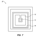
- FIG. 7 is a top plan view of the sensor of FIG. 2 , but when configured to simultaneously measure electrical field and magnetic fields;
- FIG. 8 is a graph of the voltage response output signal of the ST circuit of the sensor of FIG. 2 in absence of an external electric field
- FIG. 9 is the same graph as FIG. 8 , but in the presence of an electric field
- FIG. 10 is a graph of voltage response the ring configuration of FIG. 4 in the absence of an external electric field
- FIG. 11 is the same graph as FIG. 10 , but in the presence of an electric field.
- FIG. 12 is a block diagram of steps that can be taken to practice the methods of the present invention according to several embodiments.
- MF multiferroic
- magnetoelectric multiferroics in which the ferroelectric and ferromagnetic orders not only coexist in the same material, but are also coupled to each other such that an E-field can induce a magnetization and a B-field can induce a polarization.
- magneto-electric effect then, can be used to describe any form of cross-correlation between magnetic and dielectric properties.
- the perovskite phase of BiFeO 3 can be unique. This is because BFO is an antiferromagnetic material, but the addition of Dy to the BFO can change the ordering from antiferromagnetic to ferromagnetic, and can result in a multiferroic material that can often exhibit magnetoelectric coupling at room temperature.
- a large spontaneous electric polarization 60 ⁇ Ccm ⁇ 2
- a substantial thickness-dependent saturation magnetization 150 emucm ⁇ 3
- the inventors of the present invention according to several embodiments conceived of the idea of exploiting hysteretic behaviors of the multiferroic materials by using the multiferroic materials as ferroelectric capacitors for E-field sensing.
- a nonlinear ring oscillator underpinned by ferroelectric capacitors has been developed and characterized for its ability to measure weak electric fields.
- the present invention can focus on the change of the ferroelectric hysteresis with an applied B-field.
- the present invention can show that the magneto-electric effect of BDFO (BDFO is described as an example, but other multiferroic materials could be used) can be opportunistically exploited to detect and quantify an external B-field through the change that it produces in the electrical order.
- BDFO magneto-electric effect
- a theoretical phenomenological model of hysteretic behavior which can be based on the empirical data of BDFO material can be developed. The model can be used to quantify the response, to a B-field, of a single BDFO-based capacitive sensor.
- the ring configuration can afford enhanced sensitivity (compared to a single ST circuit) to small changes in the ambient B-field (For purposes of this disclosure, an ST circuit can be defined as a circuit that can convert polarization to a voltage in order to quantify (measure) polarization).
- thin film BDFO devices can be subject to different values of DC B-fields (as perturbations to the ambient DC B-field) and the polarization (P) versus E-field (E) hysteresis loops can be obtained for each case.
- good magnetoelectric coupling can be observed, i.e., the (ferroelectric) hysteresis loops characteristics change with the applied B-fields.
- Equation (1) can correspond to the particle-in-potential paradigm with U(P,t) being the (bistable) potential energy function, and the materials-based parameters (a, b) must be positive to ensure bistability.
- the parameters (a,b,c) can be phenomenological coefficients calculated via a fitting algorithm to ensure the good agreement between the experimentally obtained hysteresis and its theoretically model.
- “c” can be a materials-based parameter that quantifies the effect of the external electric field on the multiferroic polarization.
- “ ⁇ ” can represent the device time-constant, and “ ⁇ ” can be a phase-lag between the input and output (introduced by the prior art test equipment).
- E the driving term
- the width of the hysteresis loop between its intersections of 0
- coercivity E c ⁇ square root over (4a 2 r i 2 /27) ⁇
- width of the hysteresis loop between its intersections of the E axis
- U 0 /2r coercivity
- a simplex parameter identification procedure can be used to obtain a theoretical representation of the dynamics that underpin the experimentally obtained hysteresis loops by Palkar et al. in the prior art.
- the theoretical representations can be illustrated as hysteresis loops 14 a , 14 b and 14 c in FIG. 1 .
- Fig. shows the experimentally obtained hysteresis loops together with the numerical fit using Equation (1)
- ST circuit 20 can include a multiferroic capacitor 22 , represented by C MF .
- a MF capacitor can be a capacitor that includes a multiferroic layer.
- a multiferroic layer is a layer can be a material that is multiferroic, such as BDFO. Other multiferroic layers could be used, provided such materials exhibit the hysteresis behavior described above.
- multiferroic capacitor 22 can function as the active nonlinear element
- C f can represent the feedback capacitor 24 used to fix the working point of the circuit 20
- the resistor 26 R f can be introduced to avoid drift in the circuit output.
- the frequency response of the ST circuit 20 can be given by
- V out - A MF C f ⁇ P , ( 3 )
- a MF can be the surface area of the electrode (the multiferroic layer) of the MF capacitor.
- the term “ring” or “ring configuration” shall mean that for each ST circuit 20 in ring configuration 40 the output of one ST circuit 20 in ring configuration 40 shall be the input of another ST circuit 20 .
- the term “ring” or “ring configuration” shall mean that for each ST circuit 20 in ring configuration 40 the output of one ST circuit 20 in ring configuration 40 shall be the input of another ST circuit 20 .
- ⁇ c ⁇ A MF d ⁇ ⁇ C f ⁇ k .
- ⁇ can therefore be a tunable parameter, where varying the c, A MF , (“d” is the thickness of the multiferroic layer) or C f parameters can vary ⁇ .
- Equation (4) can be simulated using Simulink (other types of software known in the art for this purpose) by using the material a, b, c and ⁇ parameters from Table 1 from the measurements taken on the MF samples.
- Simulink results therefore, can be highly representative of the real system behavior.
- the application of an external target B-field corresponds to a change in the material parameters in accordance with the listings in Table 1.
- the solutions of Equations (4) can be oscillatory (although not sinusoidal, see FIG. 5 ) unless ⁇ >> ⁇ . But when ⁇ >> ⁇ c , and as shown in FIG. 6 , the solutions of Equation (4) can be both oscillatory and sinusoidal, with amplitude and period dependent on the parameters (a, b, ⁇ ). Thus, the oscillation characteristics might be useful to quantify the external magnetic field B, via the changes in their characteristics induced by changing the parameters listed in Table 1.
- the oscillations in the 3 elements P i are separated in phase by 2 ⁇ /N, and the period T can be shown to scale according to the relationship 1/ ⁇ square root over (
- the amplitude and frequency of the oscillations generated for three cases of applied DC B-field, where the case were obtained through numerical simulation of the coupled system with BDFO capacitors from Table 1 (a, b, c and ⁇ ) can be described in Table 2 below.
- Table 2 can also show the values of ⁇ corresponding to each value of the B-field.
- the change in B-field can be quantified through the change in the oscillation frequency and especially through the change in amplitude of curves 52 .
- the sensitivity of the output frequency and amplitude, respectively, with regard to an applied change in external B-field can be estimated as
- the output amplitude and frequency can increase with the coupling gain k; therefore k can be a tunable parameter to make the system work in a desired range of frequency or amplitude.
- the multiferroic capacitor 22 can be divided into a bias portion 72 and a sensing portion 74 , which can be deposed onto substrate 76 .
- Sensing portion 74 can include a charge collector for sensing electric field, such as Lead zirconium titanate, or PZT, as well as a magnetostrictive layer such as an alloy of the formula Tb x Dy 1-x Fe 2 (x ⁇ 0.3), more commonly referred to as Terfenol-D,
- a charge collector for sensing electric field, such as Lead zirconium titanate, or PZT, as well as a magnetostrictive layer such as an alloy of the formula Tb x Dy 1-x Fe 2 (x ⁇ 0.3), more commonly referred to as Terfenol-D.
- the addition of a charge collector can increase the sensitivity of the device to external electric fields, and can allow sensing of a target external electric field that will appear as an AC ripple over the output voltage of the ST circuit, while the magnetic field will be measured through the estimation of the peak value.
- FIG. 7 illustrates an example of such a layout.
- an AC electric field can modulate the output of the sensor, yielding a slow modulating wave, which can be superimposed on the magnetic field induced oscillations, and whose characteristics can depend on the external electric field (or on the external electric polarization).
- Measures of the magnetic field and of the electric field can be performed simultaneously, because the amplitude and the frequency of the carrier wave depend on the magnetic field, while the (modulating) wave ripple and its frequency depend on the electric field.
- FIGS. 8 and 9 can illustrate these phenomena.
- FIG. 8 depicts a representative output signal of the ST circuit 20 in absence of an external electric field
- FIG. 9 depicts the output signal of ST circuit 20 in presence of an electric field. Simulations were performed for an external magnetic field of 0.01 T, imposing an external sinusoidal polarization of 5 mC/cm 2 amplitude and a frequency of 1 Hz. Simulations were performed to verify that the sensor output changes with an imposed target electric field.
- FIGS. 10 and 11 illustrate the behavior of ring 40 configuration of ST circuits 20 in the presence of an external electric field. Simulations were performed with Simulink software. The results are reported in FIGS. 10 and 11 .
- FIG. 10 illustrates the output signal of the coupled ring 40 in absence of an external electric field
- FIG. 11 illustrate the output signal of ring 40 in presence of an electric field. Simulations were performed for an external magnetic field of 0.01 T, imposing an external sinusoidal polarization of 5 mC/cm 2 amplitude and a frequency of 1 Hz.
- the external electric field can modulate the outputs of the multiferroic devices adding a ripple, whose amplitude and frequency depend on the amplitude and frequency of the target electric field.
- Table 4 reports the results obtained by imposing three different electric polarization values. As shown in Table 4, the ripple amplitude A r can increase with the external electric field value.
- method 80 can include the initial step 82 of determining the dynamical parameters for the ferroelectrical component multiferroic capacitor. Landau-Khalatnikov theory can be used to accomplish this step.
- the methods can include the step of obtaining in material parameters of the multiferroic layer, as shown by step 84 . Once the parameters have been obtained, the methods can include the step of crafting the multiferroic capacitor for ST circuit 20 , as shown by block 86 . This step can be accomplished by epitaxially growing BDFO or similar type material on a SrTiO 3 substrate.
- the BDFO surface area A MF for multiferroic capacitor 22 can be chosen according to the parameters of step 84 .
- the methods can further include the steps of incorporating the multiferroic capacitor 22 into an ST circuit 20 (steps 88 ) and coupling an odd number of crafted ST circuits 20 in a ring 40 configuration, as shown by step 90 .
- the odd number of crafted ST circuit can be chosen according to the level in impurities in the multiferroic layer of multiferroic capacitor 22 and the desired size and sensitivity of the device.
Landscapes
- Physics & Mathematics (AREA)
- General Physics & Mathematics (AREA)
- Condensed Matter Physics & Semiconductors (AREA)
- Measuring Magnetic Variables (AREA)
Abstract
Description
Equation (1) can correspond to the particle-in-potential paradigm with U(P,t) being the (bistable) potential energy function, and the materials-based parameters (a, b) must be positive to ensure bistability. The parameters (a,b,c) can be phenomenological coefficients calculated via a fitting algorithm to ensure the good agreement between the experimentally obtained hysteresis and its theoretically model. “c” can be a materials-based parameter that quantifies the effect of the external electric field on the multiferroic polarization. “τ” can represent the device time-constant, and “φ” can be a phase-lag between the input and output (introduced by the prior art test equipment). In the absence of the driving term (i.e., E=0 which can cause “c” to be 0), the width of the hysteresis loop (between its intersections of 0) the stable minima of the potential function can occur at ±ri=±√{square root over (b/a)}, and the energy barrier height can be U0=a2/4b. The connection to the hysteresis loop is made by noting that coercivity Ec=±√{square root over (4a2ri 2/27)}, while the width of the hysteresis loop (between its intersections of the E axis) can be proportional to U0/2r. Thus, a simplex parameter identification procedure can be used to obtain a theoretical representation of the dynamics that underpin the experimentally obtained hysteresis loops by Palkar et al. in the prior art. The theoretical representations can be illustrated as
| TABLE 1 | |||
| Magnetic Field | 0T | 0.01T | 0.02T |
| a | 8.967 × 10⁻⁷ | 1.029 × 10⁻² | 1.133 × 10⁻² |
| b | 3.936 × 10⁻⁴ | 1.421 × 10⁻⁴ | 1.260 × 10⁻⁴ |
| c | −2.250 × 10⁻⁷ | −2.395 × 10⁻⁷ | −2.459 × 10⁻⁷ |
| T | 1.259 × 10⁻² | 1.013 × 10⁻² | 8.507 × 10⁻³ |
Choosing Rf>>(sCf)−1, it can be shown that
where AMF can be the surface area of the electrode (the multiferroic layer) of the MF capacitor.
τ{dot over (P)} i =aP i =bP i 3 +λP i-1 :i=1 . . . 3. (4)
where, taking Equations (1) and (3) into account, the coupling strength can be expressed in terms of a (negative) gain k as
λ can therefore be a tunable parameter, where varying the c, AMF, (“d” is the thickness of the multiferroic layer) or Cf parameters can vary λ.
T i =N√{square root over (2)}π[|f(P 10)f″(P 10)|−1/2 +|f(−P 10)f″(−P 10)|−1/2], (5)
where f(P1) can be defined as aP1−bP1 3−λP2m (see Equation 4), P2m=√{square root over ((a+λ)/b)}, P10=√{square root over (a/3b)} and the primes denote differentiation with respect to P1. The oscillations in the 3 elements Pi are separated in phase by 2π/N, and the period T can be shown to scale according to the
| TABLE 2 | |||||
| Magnetic Field | Coupling Factor | Frequency | Amplitude | ||
| B (T) | λ (k = 40) | (Hz) | (mVpp) | ||
| 0 | 0.036 | 0.4 | 9 | ||
| 0.01 | 0.038 | 0.5 | 16 | ||
| 0.02 | 0.039 | 0.6 | 18 | ||
Using the data above, and referring to the changes in the B-field around zero, a sensitivity of 7V/T with respect to output voltage can be obtained, which can correspond to a change in the output voltage of 77% for a change of 0.01 T in the B-field. This can confirm that the change in the oscillation amplitude might be the better indicator of a change in the applied magnetic signal (field). Referring briefly back to
| TABLE 3 | |||
| Electric Polarization | |||
| (mC/cm2) | Ripple Amplitude (mV) | ||
| 5 | 29 | ||
| 10 | 55 | ||
| 15 | 77 | ||
| TABLE 4 | |||
| Electric Polarization (mC/cm2) | Ripple Amplitude (mV) | ||
| 5 | 22 | ||
| 10 | 42 | ||
| 15 | 60 | ||
Analogous to the case of a magnetic field sensor, when the target field is an electric polarization the sensitivity can be evaluated considering the following equation:
S P Ar=100((ΔA r /A rmax)/(ΔP/P max)) (7)
Where Ar is the ripple amplitude and P is the external polarization. Noting that the amplitude of the oscillations is larger in the coupled system than in the single system, we find a sensitivity of 95% in this case compared to 93% for the single circuit case Thus, the responsivity can be slightly larger in the coupled case.
Claims (8)
Priority Applications (1)
| Application Number | Priority Date | Filing Date | Title |
|---|---|---|---|
| US14/543,409 US9470733B2 (en) | 2014-11-17 | 2014-11-17 | Sensor incorporating multiferroic materials for detecting both electric and magnetic fields |
Applications Claiming Priority (1)
| Application Number | Priority Date | Filing Date | Title |
|---|---|---|---|
| US14/543,409 US9470733B2 (en) | 2014-11-17 | 2014-11-17 | Sensor incorporating multiferroic materials for detecting both electric and magnetic fields |
Publications (2)
| Publication Number | Publication Date |
|---|---|
| US20160139190A1 US20160139190A1 (en) | 2016-05-19 |
| US9470733B2 true US9470733B2 (en) | 2016-10-18 |
Family
ID=55961455
Family Applications (1)
| Application Number | Title | Priority Date | Filing Date |
|---|---|---|---|
| US14/543,409 Expired - Fee Related US9470733B2 (en) | 2014-11-17 | 2014-11-17 | Sensor incorporating multiferroic materials for detecting both electric and magnetic fields |
Country Status (1)
| Country | Link |
|---|---|
| US (1) | US9470733B2 (en) |
Cited By (1)
| Publication number | Priority date | Publication date | Assignee | Title |
|---|---|---|---|---|
| US20200002845A1 (en) * | 2014-05-28 | 2020-01-02 | Board Of Regents, The University Of Texas System | Tuned materials, tuned properties, and tunable devices from ordered oxygen vacancy complex oxides |
Families Citing this family (3)
| Publication number | Priority date | Publication date | Assignee | Title |
|---|---|---|---|---|
| US10401396B2 (en) * | 2015-03-11 | 2019-09-03 | Mee H. CHOI | Weakly-bistable signal detectors having one or an even-number of stages |
| US12272520B2 (en) * | 2019-07-09 | 2025-04-08 | Tokyo Electron Limited | Process control enabled VDC sensor for plasma process |
| CN115611357B (en) * | 2022-10-27 | 2024-09-24 | 华东交通大学 | Photocatalytic/coagulation integrated water treatment process |
Citations (17)
| Publication number | Priority date | Publication date | Assignee | Title |
|---|---|---|---|---|
| US5487030A (en) * | 1994-08-26 | 1996-01-23 | Hughes Aircraft Company | Ferroelectric interruptible read memory |
| US5966318A (en) * | 1996-12-17 | 1999-10-12 | Raytheon Company | Nondestructive readout memory utilizing ferroelectric capacitors isolated from bitlines by buffer amplifiers |
| US6028783A (en) * | 1997-11-14 | 2000-02-22 | Ramtron International Corporation | Memory cell configuration for a 1T/1C ferroelectric memory |
| US6149774A (en) * | 1998-06-10 | 2000-11-21 | Delsys Pharmaceutical Corporation | AC waveforms biasing for bead manipulating chucks |
| US6327558B1 (en) * | 1997-12-26 | 2001-12-04 | Rohm Co., Ltd. | Apparatus for simulating electrical characteristics of a circuit including a ferroelectric device and a method for simulating electrical characteristics of a circuit including a ferroelectric device |
| US20040016889A1 (en) * | 2002-07-25 | 2004-01-29 | Delphi Technologies, Inc. | Apparatus and method for generating an amplified effect in response to a periodic stimulus applied to asymmetrical hysteretic systems |
| US20040178841A1 (en) * | 2003-03-13 | 2004-09-16 | Mantese Joseph V. | Circuit device comprising multiple polarization-graded ferroelectric elements and method of using |
| US7345475B2 (en) * | 2006-03-17 | 2008-03-18 | University Of Maryland | Ultrasensitive magnetoelectric thin film magnetometer and method of fabrication |
| US7420366B1 (en) | 2004-06-18 | 2008-09-02 | The United States Of America As Represented By The Secretary Of The Navy | Coupled nonlinear sensor system |
| US7528606B1 (en) | 2007-04-04 | 2009-05-05 | The United States Of America As Represented By The Secretary Of The Navy | Coupled nonlinear sensor system for sensing a time-dependent target signal and method of assembling the system |
| US20110008008A1 (en) * | 2009-07-07 | 2011-01-13 | Alcatel-Lucent Usa, Inc. | Multiferroic materials for tunable permittivity or permeability |
| US7898250B2 (en) | 2004-06-18 | 2011-03-01 | The United States Of America As Represented By The Secretary Of The Navy | Coupled fluxgate magnetometers for DC and time-varying target magnetic field detection |
| US20110187553A1 (en) * | 2008-07-31 | 2011-08-04 | Halliburton Energy Services, Inc. | Method and system of an electromagnetic telemetry |
| US8049586B2 (en) | 2008-08-26 | 2011-11-01 | National Tsing Hua University | Magnetic coupler |
| US20120098589A1 (en) * | 2008-12-02 | 2012-04-26 | Spanier Jonathan E | Ferroelectric nanoshell devices |
| US20140159713A1 (en) * | 2012-11-28 | 2014-06-12 | Maritime Applied Physics Corporation | High sensitivity magnetoelectric magnetometer |
| US8803264B1 (en) * | 2010-05-27 | 2014-08-12 | University Of Puerto Rico | Room-temperature magnetoelectric multiferroic thin films and applications thereof |
-
2014
- 2014-11-17 US US14/543,409 patent/US9470733B2/en not_active Expired - Fee Related
Patent Citations (17)
| Publication number | Priority date | Publication date | Assignee | Title |
|---|---|---|---|---|
| US5487030A (en) * | 1994-08-26 | 1996-01-23 | Hughes Aircraft Company | Ferroelectric interruptible read memory |
| US5966318A (en) * | 1996-12-17 | 1999-10-12 | Raytheon Company | Nondestructive readout memory utilizing ferroelectric capacitors isolated from bitlines by buffer amplifiers |
| US6028783A (en) * | 1997-11-14 | 2000-02-22 | Ramtron International Corporation | Memory cell configuration for a 1T/1C ferroelectric memory |
| US6327558B1 (en) * | 1997-12-26 | 2001-12-04 | Rohm Co., Ltd. | Apparatus for simulating electrical characteristics of a circuit including a ferroelectric device and a method for simulating electrical characteristics of a circuit including a ferroelectric device |
| US6149774A (en) * | 1998-06-10 | 2000-11-21 | Delsys Pharmaceutical Corporation | AC waveforms biasing for bead manipulating chucks |
| US20040016889A1 (en) * | 2002-07-25 | 2004-01-29 | Delphi Technologies, Inc. | Apparatus and method for generating an amplified effect in response to a periodic stimulus applied to asymmetrical hysteretic systems |
| US20040178841A1 (en) * | 2003-03-13 | 2004-09-16 | Mantese Joseph V. | Circuit device comprising multiple polarization-graded ferroelectric elements and method of using |
| US7420366B1 (en) | 2004-06-18 | 2008-09-02 | The United States Of America As Represented By The Secretary Of The Navy | Coupled nonlinear sensor system |
| US7898250B2 (en) | 2004-06-18 | 2011-03-01 | The United States Of America As Represented By The Secretary Of The Navy | Coupled fluxgate magnetometers for DC and time-varying target magnetic field detection |
| US7345475B2 (en) * | 2006-03-17 | 2008-03-18 | University Of Maryland | Ultrasensitive magnetoelectric thin film magnetometer and method of fabrication |
| US7528606B1 (en) | 2007-04-04 | 2009-05-05 | The United States Of America As Represented By The Secretary Of The Navy | Coupled nonlinear sensor system for sensing a time-dependent target signal and method of assembling the system |
| US20110187553A1 (en) * | 2008-07-31 | 2011-08-04 | Halliburton Energy Services, Inc. | Method and system of an electromagnetic telemetry |
| US8049586B2 (en) | 2008-08-26 | 2011-11-01 | National Tsing Hua University | Magnetic coupler |
| US20120098589A1 (en) * | 2008-12-02 | 2012-04-26 | Spanier Jonathan E | Ferroelectric nanoshell devices |
| US20110008008A1 (en) * | 2009-07-07 | 2011-01-13 | Alcatel-Lucent Usa, Inc. | Multiferroic materials for tunable permittivity or permeability |
| US8803264B1 (en) * | 2010-05-27 | 2014-08-12 | University Of Puerto Rico | Room-temperature magnetoelectric multiferroic thin films and applications thereof |
| US20140159713A1 (en) * | 2012-11-28 | 2014-06-12 | Maritime Applied Physics Corporation | High sensitivity magnetoelectric magnetometer |
Non-Patent Citations (7)
| Title |
|---|
| A. Beninato et al., A Concept for a Magnetic Field Detector Underpinned by the Nonlinear Dynamics of Coupled Multiferroic Devices, Applied Physics Letters 103, 244107, pp. 244107-1 to 244107-4, Dec. 13, 2013, online. |
| B. Ando et al., A Coupled Nonlinear Circuit for E-Field and B-Field Detection, Sensors Applications Symposium (SAS), 2014 IEEE , vol., No., pp. 223-227 (ISBN 978-1-4799-2180-5), Feb. 18-20, 2014, Queenstown, New Zealand. |
| Carlo Trigona et al., Exploiting Nonlinear Dynamics in Novel Measurement Strategies and Devices: From Theory to Experiments and Applications, IEEE Transactions on Instrumentation and Measurement, (IEEE), 2011 60 (3), pp. 667-695. |
| J.T. Evans, Jr., Operating the Radiant TO-18 Sawyer-Tower Board, Radiant Technologies, Inc. PowerPoint(R) Presentation, Apr. 5, 2013, http://www.ferromems.com/1/360/files/Sawyer-TowerBoardDescription.pdf. |
| K. K Prashanthi, S.P. Duttagupta, R. Pinto and V.R. Palkar (Multiferroic Bi0.7Dy0.3FeO3 films as high k dielectric material for advanced non-volatile memory devices) Electronics Letters Jul. 30, 2009 vol. 45 No. 16. * |
| V.C. Lo, Simulation of Thickness Effect in Thin Ferroelectric Films Using Landau-Khalatnikov Theory, Journal of Applied Physics, vol. 94, No. 5, pp. 3353-3359, Sep. 1, 2003, online. |
| V.R. Palkar et al., Observation of Magnetoelectric Coupling in Bi0.7Dy0.3FeO3 (BDFO) Thin Films at Room Temperature, Applied Physics Letters 93, 132906, pp. 132906-1 to 132906-3, (2008), online. |
Cited By (1)
| Publication number | Priority date | Publication date | Assignee | Title |
|---|---|---|---|---|
| US20200002845A1 (en) * | 2014-05-28 | 2020-01-02 | Board Of Regents, The University Of Texas System | Tuned materials, tuned properties, and tunable devices from ordered oxygen vacancy complex oxides |
Also Published As
| Publication number | Publication date |
|---|---|
| US20160139190A1 (en) | 2016-05-19 |
Similar Documents
| Publication | Publication Date | Title |
|---|---|---|
| Hu et al. | Understanding and designing magnetoelectric heterostructures guided by computation: progresses, remaining questions, and perspectives | |
| KR101701145B1 (en) | Negative capacitance logic device, clock generator including the same and method of operating the clock generator | |
| US9470733B2 (en) | Sensor incorporating multiferroic materials for detecting both electric and magnetic fields | |
| US8076930B2 (en) | Thin film 3 axis fluxgate and the implementation method thereof | |
| EP2503556B1 (en) | Memristive system | |
| Patel et al. | A technique for giant mechanical energy harvesting using ferroelectric/antiferroelectric materials | |
| KR101532150B1 (en) | Othogonal type fluxgate sensor | |
| Burdin et al. | High-sensitivity dc field magnetometer using nonlinear resonance magnetoelectric effect | |
| Darbaniyan et al. | Designing soft pyroelectric and electrocaloric materials using electrets | |
| Fetisov et al. | Nonlinear magnetoelectric effects in flexible composite ferromagnetic–piezopolymer structures | |
| Zhuang et al. | Mechanical noise limit of a strain-coupled magneto (elasto) electric sensor operating under a magnetic or an electric field modulation | |
| Yu et al. | A slice-type magnetoelectric laminated current sensor | |
| Liu et al. | Giant and universal magnetoelectric coupling in soft materials and concomitant ramifications for materials science and biology | |
| Balakrishna et al. | Nanoscale domain patterns and a concept for an energy harvester | |
| Yao et al. | Influence of magnetic fields on the mechanical loss of Terfenol-D/PbZr0. 52Ti0. 48O3/Terfenol-D laminated composites | |
| Lv et al. | Magnetoelectric Pb (Zr0. 52Ti0. 48) O3–La0. 65Sr0. 35MnO3 composite thin films derived by the pulse laser deposition method | |
| US8049486B1 (en) | Coupled electric field sensors for DC target electric field detection | |
| Lou et al. | A wide-range DC current sensing method based on disk-type magnetoelectric laminate composite and magnetic concentrator | |
| Kumar et al. | In-plane strain modulated magnetization and magnetoelectric effect in La0. 7Sr0. 3MnO3-BaTiO3 and La0. 7Sr0. 3MnO3-BaTiO3-BiFeO3 multilayer's | |
| Chen et al. | Fabrication and characterization of shape anisotropy AlN/FeCoSiB magnetoelectric composite films | |
| Kaeswurm et al. | The anhysteretic polarisation of ferroelectrics | |
| Onuta et al. | Dynamic state switching in nonlinear multiferroic cantilevers | |
| Ma et al. | A novel frequency multiplier based on magnetoelectric laminate | |
| Zhou et al. | Magnetoelectric response in a new tunable capacitor system based on magnetostrictive material and electret | |
| US7064950B2 (en) | Circuit device comprising multiple polarization-graded ferroelectric elements and method of using |
Legal Events
| Date | Code | Title | Description |
|---|---|---|---|
| AS | Assignment |
Owner name: UNITED STATES OF AMERICA AS REPRESENTED BY THE SEC Free format text: ASSIGNMENT OF ASSIGNORS INTEREST;ASSIGNORS:BULSARA, ADI RATAN;EMERY, TERESA;REEL/FRAME:034190/0169 Effective date: 20141117 |
|
| STCF | Information on status: patent grant |
Free format text: PATENTED CASE |
|
| MAFP | Maintenance fee payment |
Free format text: PAYMENT OF MAINTENANCE FEE, 4TH YEAR, LARGE ENTITY (ORIGINAL EVENT CODE: M1551); ENTITY STATUS OF PATENT OWNER: LARGE ENTITY Year of fee payment: 4 |
|
| FEPP | Fee payment procedure |
Free format text: MAINTENANCE FEE REMINDER MAILED (ORIGINAL EVENT CODE: REM.); ENTITY STATUS OF PATENT OWNER: LARGE ENTITY |
|
| LAPS | Lapse for failure to pay maintenance fees |
Free format text: PATENT EXPIRED FOR FAILURE TO PAY MAINTENANCE FEES (ORIGINAL EVENT CODE: EXP.); ENTITY STATUS OF PATENT OWNER: LARGE ENTITY |
|
| STCH | Information on status: patent discontinuation |
Free format text: PATENT EXPIRED DUE TO NONPAYMENT OF MAINTENANCE FEES UNDER 37 CFR 1.362 |
|
| FP | Lapsed due to failure to pay maintenance fee |
Effective date: 20241018 |