EP2493268B1 - Lighting device and luminaire - Google Patents
Lighting device and luminaire Download PDFInfo
- Publication number
- EP2493268B1 EP2493268B1 EP12155743.3A EP12155743A EP2493268B1 EP 2493268 B1 EP2493268 B1 EP 2493268B1 EP 12155743 A EP12155743 A EP 12155743A EP 2493268 B1 EP2493268 B1 EP 2493268B1
- Authority
- EP
- European Patent Office
- Prior art keywords
- power supply
- circuit
- lamp
- voltage
- threshold
- Prior art date
- Legal status (The legal status is an assumption and is not a legal conclusion. Google has not performed a legal analysis and makes no representation as to the accuracy of the status listed.)
- Not-in-force
Links
Images


Classifications
-
- H—ELECTRICITY
- H05—ELECTRIC TECHNIQUES NOT OTHERWISE PROVIDED FOR
- H05B—ELECTRIC HEATING; ELECTRIC LIGHT SOURCES NOT OTHERWISE PROVIDED FOR; CIRCUIT ARRANGEMENTS FOR ELECTRIC LIGHT SOURCES, IN GENERAL
- H05B45/00—Circuit arrangements for operating light-emitting diodes [LED]
- H05B45/50—Circuit arrangements for operating light-emitting diodes [LED] responsive to malfunctions or undesirable behaviour of LEDs; responsive to LED life; Protective circuits
Definitions
- Embodiments described herein relate generally to a lighting device that can light illumination lamps irrespective of the number thereof, and a luminaire including the lighting device.
- the load abnormality When the load abnormality occurs, the load abnormality is detected and the illumination lamp lighting device can be made to perform the protecting operation.
- the load abnormality is detected by monitoring the output voltage of the power supply circuit, in general, a threshold is set, and when the output Voltage deviates from the threshold, a determination is made that there is an abnormality.
- a request may be made to enable a specified number of illumination lamps different from each other in lamp voltage within a range of 45 to 95V to be lit by using the same power supply circuit.
- the threshold of the illumination lamp lighting device is fixed, if the illumination lamps are enabled to be lit irrespective of the number thereof, an appropriate protecting operation can not be performed.
- An object of an exemplary embodiment is to provide a lighting device and a luminaire, which applies thresholds corresponding to the connected lamp number of illumination lamps and can appropriately control a power supply circuit.
- a lighting device includes a direct-current power supply device, a first Voltage detection circuit, a second Voltage detection circuit and a control circuit.
- the direct-current power supply device includes a constant-current controlled power supply circuit and a pair of illumination lamp connection parts, and each of the pair of illumination lamp connection parts includes a pair of terminals to which an illumination lamp can be individually connected.
- One of the terminals of one of the illumination lamp connection parts is connected to a positive output end of the power supply circuit, and the other of the terminals is connected to a non-potential connection end.
- One of the terminals of the other of the illumination lamp connection parts is connected to the non-potential connection end, and the other of the terminals is connected to a negative output end of the power supply circuit.
- a pair of illumination lamps are connected in series between the positive output end and the negative output end of the power supply circuit through the non-potential connection end.
- the first voltage detection circuit detects a voltage between the positive output end and the negative output end of the power supply circuit.
- the second voltage detection circuit detects a voltage between the non-potential connection end and the positive output end or the negative output end.
- the control circuit includes a threshold for a case where the pair of illumination lamps are connected in series between the positive output end and the negative output end of the power supply circuit, and a threshold for a case where the one illumination lamp is connected between the positive output end and the negative output end of the power supply circuit.
- the control circuit determines the connected lamp number of the illumination lamps to the direct-current power supply device based on detection outputs of the first and the second voltage detection circuit, and selects the threshold corresponding to the connected lamp number to control the direct-current power supply device.
- the lighting device and the luminaire can be provided in which the threshold corresponding to the connected lamp number of illumination lamps is applied and the power supply circuit can be appropriately controlled.
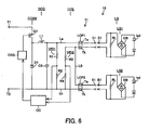
- a luminaire 10 includes an LED lamp LS as an illumination lamp and a lighting device 11 to light the illumination lamp LS.
- the lighting device 11 is configured such that the two-lamp type or one-lamp type LED lamp LS is selectively connected to a direct-current power supply device DCS and can be lit.
- the lighting device includes the direct-current power supply device DCS, a first and a second voltage detection circuit VfD1, VfD2 and a control circuit CC.
- the LED lamp LS is preferably used for lighting in this embodiment, the lamp may be used for another use by request.
- the LED lamp LS to be used includes LEDs led, and the number thereof is not specifically limited. Accordingly, a desired number of LEDs led may be provided in order to obtain a desired amount of light.
- the plural LEDs can form a series-connected circuit or a series-parallel circuit or a parallel circuit.
- the LED lamp may include a single LED led.
- the light source of the illumination lamp is not limited to the LED, and may be an electro-luminescence (EL), an organic light-emitting diode (OLED), an organic electro-luminescence (OEL) or the like.
- the LED lamp LS includes a power receiving end for connection with an output end of the direct-current power supply device DCS.
- the power receiving end has preferably a form of a cap, no limitation is made to this.
- the cap structures complying with well-known various cap standards can be adopted by request.
- the power receiving end may have a form of a connector extended through a conductive wire from the main body of the LED lamp LS.
- the power receiving end may be a connection conductor itself.
- the LED lamp LS may have various forms.
- the form may be a straight tube shape in which caps are provided at both ends, or a single cap shape, as in an incandescent lamp, in which a screw cap is provided at one end.
- the DC-DC converter CONV is a circuit that generally converts an input direct-current voltage to a different direct-current voltage.
- the output voltage is applied to the LED lamp LS to light it.
- the DC-DC converter CONV functions as the main part of the power supply circuit DOC.
- the concept of the DC-DC converter CONV includes a flyback converter, a forward converter, a switching regulator or the like in addition to various choppers.
- the output of the DC-DC converter CONV is controlled and the output current is adjusted, so that the LED lamp LS can be dimmed and lit at a desired level.
- the copper has a high conversion efficiency, the circuit structure is simple and the control is easy. Accordingly, the chopper is preferable as the DC-DC converter CONV in this embodiment.
- the power supply circuit DOC can be configured such that the output of the power supply circuit DOC can be changed so as to change the direct current supplied to the LED lamp LS according to an output control signal, for example, a dimming signal. That is, the structure can be made such that a dimming signal generation circuit is provided inside or outside the direct-current power supply device DCS, and the LED lamp LS is dimmed and lit according to the dimming signal sent from the circuit.
- the dimming signal may be modulated by using a PWM modulation system.
- the power supply circuit DOC is configured such that even if the LED lamp LS having a lamp voltage of 45 to 95V is connected to the output end, this lamp can be normally lit.
- the power supply circuit DOC is constant-current controlled, so that the output voltage is changed correspondingly to the lamp voltage of the LED lamp LS.
- each of the LED lamp connection parts LCP 1 and LCP 2 includes a pair of terminals Ta and Tk.
- the pair of terminals Ta and Tk are preferably disposed to be relatively close to each other so that the terminals are easily differentiated from the other LED lamp connection part when the terminals connect the LED lamp LS.
- the non-potential connection end L0 is a conductive circuit which is connected neither to the positive output end La of the power supply circuit DOC nor to the negative output end Lk in the state where the LED lamp LS is not connected, and to which the power receiving end of the LED lamp LS can be directly or indirectly connected.
- a pair of lead wires extended from each of a pair of sockets S1 and S1 are connected to each of the pair of LED lamp connection parts LCP1 and LCP2.
- the caps B1 of the LED lamps LS1 and LS2 are mounted on the sockets S1, so that the lamps are connected to the pair of LED lamp connection parts LCP1 and LCP2.
- LED lamp LS when the LED lamp LS is connected to the single LED lamp connection part LCP1 or LCP2, as shown in the mode of two-lamp type series connection of FIG. 2(b) , plural LED lamps LS11 and LS12, LS21 and LS22 are series-connected by request, and they can be respectively regarded as one-lamp type LED lamp LS1 and LS2.
- the pair of LED lamp connection parts LCP1 and LCP2 have only to be connected to the power receiving ends of the LED lamp LS directly or indirectly through, for example, the socket, and the remainder of the structure is not specifically limited.
- a form of a terminal block may be adopted.
- the connection parts are preferably contained inside a surrounding housing H such as a case to surround the power supply circuit DOC and the like.
- the first voltage detection circuit VfD1 detects a voltage between the positive and the negative output ends La and Lk of the power supply circuit DOC. Accordingly, if the LED lamp LS is connected to the power supply circuit DOC, the first voltage detection circuit VfD1 can detect the lamp voltage irrespective of the number of lamps and can detect an abnormal voltage generated when de-mounting or open mode failure of the LED lamp LS occurs.
- the second voltage detection circuit VfD2 detects a voltage between the non-potential connection end L0 and the negative output end Lk. Accordingly, as shown in FIG. 1 , if the two LED lamps LS1 and LS2 are connected in series to the direct-current power supply device DCS, the second voltage detection circuit VfD2 can detect the lamp voltage of the other LED lamp LS2 connected to the negative output end Lk and an abnormal voltage generated when de-mounting or open mode failure of the LED lamp LS occurs. Besides, as shown in FIG.
- the lamp voltage of only one LED lamp LS or the abnormal voltage generated when the open mode such as the de-mounting occurs can be detected. Accordingly, if the first voltage detection circuit VfD1 and the second voltage detection circuit VfD2 are provided, the lamp voltages of the two LED lamps LS1 and LS2 or the abnormal voltage generated when the open mode such as the de-mounting occurs can be individually detected.
- control circuit CC will be described.
- the control circuit CC has a threshold for a case where the pair of LED lamps LS1 and LS2 are connected in series to the power supply circuit DOC of the direct-current power supply device DCS, and a threshold for a case where the one LED lamp LS1 is connected as shown in FIG. 2(a) .
- these thresholds may constitute a threshold group including plural thresholds.
- the control circuit CC determines the connected lamp number of the LED lamps LS to the power supply circuit DOC based on the detection outputs of the first and the second voltage detection circuit VfD1, VfD2. Then, a threshold corresponding to the determined connected lamp number is selected, and a threshold is determined each time according to a sampling value when a lighting condition is changed.
- the power supply circuit DOC is suitably controlled so as not to deviate from the determined threshold.
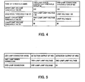
- a threshold group (a) applied in a mode of two-lamp series connection as shown in FIG. 3(a) and a threshold group (b) applied in a mode of one-lamp connection as shown in FIG. 3(b) are previously prepared in the control circuit CC.
- an upper limit value that is, an upper limit voltage threshold THU
- a lower limit value that is, a lower limit voltage threshold THL
- an open mode threshold THB and a short-circuit mode threshold THS are set.
- the upper limit voltage threshold THU and the lower limit voltage threshold THL are formed of absolute fixed values.
- the open mode threshold THB and the short-circuit threshold THS are formed of relatively variable values with respect to the lamp voltage of the LED lamp LS.
- the upper limit value, that is, the upper limit voltage threshold THU, and the lower limit value, that is, the lower limit voltage threshold THL are the absolutely fixed thresholds which are set to enable the LED lamps LS different from each other in load voltage to be lit by using the same power supply circuit DOC within the permissible range of lamp voltage of, for example, 45 to 95 V, and are set to cause the power supply circuit DOC to perform a protecting operation when an unauthorized LED lamp LS having a lamp voltage deviating from the permissible range is mounted.
- the upper limit voltage threshold THU is useful to cause the power supply circuit DOC to perform the protecting operation when an LED lamp LS having a lamp voltage of more than 95V is mounted and the lamp voltage rises and exceeds the upper limit voltage threshold THU.
- the lower limit voltage threshold THL is useful to cause the power supply circuit DOC to perform the protecting operation when an LED lamp LS having a lamp voltage of less than 45V is mounted and the lamp voltage is reduced and becomes lower than the lower limit voltage threshold THL.
- the open mode threshold THB and the short-circuit mode threshold THS are thresholds which are for the normal LED lamp LS having a lamp voltage in a range of, for example, 45 to 95V and are relatively variable according to the lamp voltage, and are the thresholds which are set to cause the power supply circuit DOC to perform the protecting operation at the time of occurrence of abnormality of the LED lamp LS during lighting.
- the open mode threshold THB is the threshold to cause the protecting operation to be performed when the lamp voltage exceeds this threshold, so that arc discharge does not occur at the time of de-mounting of the LED lamp LS or open mode failure of the LED lamp LS.
- the "de-mounting" means that the LED lamp LS mounted on the output end of the power supply circuit DOC is detached from the output end of the power supply circuit DOC because of some reason such as shock or vibration applied from the outside during lighting, or the contact becomes loose and the contact resistance becomes large.
- the arc discharge is apt to occur at that time. Since the power supply circuit DOC is constant-current controlled, when the connection is detached, an output voltage Vf of the power supply circuit DOC increases, and accordingly, the arc discharge is more apt to occur.
- the short-circuit mode threshold THS is the threshold for causing the power supply circuit DOC to perform the protecting operation when the short-circuit occurrence number of LEDs led inside the LED lamp LS deviates from a permissible range and becomes lower than this, the LED lamp is brought into such a state that the LED lamp can not be used as the light source, and the lamp voltage is reduced.
- the threshold group (a) applied in the mode of two-lamp series connection and the threshold group (b) applied in the mode of one-lamp connection are as shown in FIG. 4 .
- the thresholds are shown in FIGS. 3(a) and 3(b) in which the lamp voltage is 70V.
- a voltage of 20V added to the lamp voltage indicates an abnormal voltage rising from the lamp voltage
- the voltage may be set with some margin, and can be set within a range of, for example, 15 to 23V.
- a low voltage obtained through an auxiliary power supply circuit from the alternating-current power supply AC for example, a direct-current control voltage Vcc obtained by starting a not-shown direct-current control power supply at the time of turning on the alternating-current power supply AC prior to the power supply circuit DOC, is applied to the first and the second voltage detection circuit VfD1, VfD2 and the load circuit, that is, the LED lamp LS.
- VfD1, VfD2 the first and the second voltage detection circuit
- the connected lamp number of the LED lamps LS can be determined according to the detection outputs of the first and the second voltage detection circuit VfD1, VfD2 shown in FIG. 5 .
- the control circuit CC can select the relevant threshold group from the threshold group (a) applied to the two-lamp series connection mode and the threshold group (b) applied to the one-lamp connection mode according to the result of the connected lamp number determination.
- control circuit CC applies the thresholds of FIG. 4 corresponding to the connected lamp number during lighting of the LED lamp LS, and controls the power supply circuit DOC of the direct-current power supply device DCS.
- the control circuit causes the power supply circuit DOC of the direct-current power supply device DCS to perform the protecting operation.
- the protecting operation although it is preferably to turn off the LED lamp LS, the light output may be reduced by narrowing down the lamp current.
- control circuit CC is configured to perform the determination of the connected lamp number of the LED lamp LS, the selection of the threshold group and the control by the application, and further to perform the other operation control of the direct-current power supply device DCS.
- the open mode threshold THB and the short-circuit mode threshold THS have such characteristics that the values are changed according to the change of the lighting condition of the LED lamp LS. Then, the output voltage of the power supply circuit DOC is directly monitored, and the change of the lighting condition can be determined. In this case, when the output voltage is changed, it is necessary to accurately grasp whether the change is the normal change of the lighting condition or whether an abnormal state occurs. In order to grasp this, for example, the change amount of the output voltage or the change pattern is preferably carefully monitored.
- the change of the lighting condition of the LED lamp LS may be indirectly checked. That is, the change of the lighting condition of the LED lamp LS can be known by checking a control signal, for example, a dimming signal. Since this mode can be performed relatively easily, this is recommendable.
- the lamp replacement is preferably performed after the power supply is once turned off. If doing so, when the power supply is again turned on after the replacement of the lamp, the output voltage is monitored and the threshold can be newly set by the foregoing method.
- a suitable ramp voltage for example, a rated lamp voltage is made a reference value
- thresholds for example, the open mode threshold THB and the short-circuit mode threshold THS may be determined based on the reference value.
- control circuit CC is preferably mainly composed of a digital device, for example, a microcomputer, an analog circuit unit may be used by request.
- both the plural LED lamps LS and the one LED lamp LS can be lit, and when the lighting condition is changed, the output voltage of the power supply circuit DOC is sampled, and the threshold is determined according to the sampling value each time.
- the threshold is again set in accordance with the change, and the power supply circuit DOC can perform the protecting operation when the output voltage is changed and deviates from the threshold.
- a DC-DC converter CONV of a power supply circuit DOC constitutes a step-down chopper
- each of a first and a second voltage detection circuit VfD1, VfD2 is composed of a voltage dividing circuit
- a pair of LED lamps LS1 and LS2 include a substantial structure.
- Each of the pair of LED lamps LS1 and LS2 includes a bleeder resistor RL and a diode bridge DB connected in parallel.
- the bleeder resistor RL can facilitate the detection of the first and the second voltage detection circuit VfD1, VfD2 when the LED lamp LS is connected to lamp connection parts LCP1 and LCP2.
- the diode bridge DB causes the connection of the LED lamp LS to a positive output end La and a negative output end Lk of the power supply circuit DOC to have no polarity.
- step-down chopper a series circuit of a switching element Q1, an inductor L1 and an output capacitor C3 is connected to input ends T1 and T2.
- the switching element Q1 is supplied with a drive signal from a drive signal generation circuit DSG and performs a switching operation.
- a series circuit of a diode D1 and the output capacitor C3 is connected in parallel to the inductor L1 in an illustrated polarity, and a closed circuit of those is formed.
- the pair of the positive output end La and the negative output end Lk of the DC-DC converter CONV of the power supply circuit DOC are extracted from both ends of the output capacitor C3.
- Sockets S1 are connected to terminals Ta and Tk of each of the pair of lamp connection parts LCP1 and LCP2 through conductive wires. Accordingly, caps B1 of the two LED lamps LS1 and LS2 are mounted on the sockets S1 so that the LED lamps are connected to the pair of lamp connection parts LCP1 and LCP2 and are mechanically supported.
- the first voltage detection circuit VfD1 is configured such that a series circuit of resistors R1 and R2 is connected between the positive output end La and the negative output end Lk of the power supply circuit DOC, and the voltage of the resistor R2 is control-inputted as a detection output to a control circuit CC.
- a capacitor is connected in parallel to the resistor R2, and the detection output is averaged.
- the control circuit CC is composed of a microcomputer that receives a direct-current control voltage Vcc from an auxiliary power supply circuit connected to an alternating-current power supply AC and operates. Besides, the control circuit CC is configured to control the power supply circuit DOC by controlling the drive signal generation circuit DSG.
- the connected lamp number determination is performed mainly by the control circuit CC. That is, based on the condition shown in FIG. 5 and according to sampling values obtained from the detection outputs of the first and the second voltage detection circuit VfD1, VfD2, the control circuit CC determines whether the LED lamp LS connected to the pair of LED lamp connection parts LCP1 and LCP2 has one lamp or two lamps in the direct-current power supply device DCS.
- the detection outputs of the first and the second voltage detection circuit VfD1, VfD2 are values obtained by averaging the terminal voltages of the resistors R2 and R4 of FIG. 6 by the not-shown capacitors connected in parallel to the resistors R2 and R4. The values are sampled for a specified time, so that the averaged sampling values are obtained.
- the control circuit CC shifts to the left side in FIG. 7 , and determines that the thresholds shown in FIG. 3(b) are applied. If the LED lamp LS has two-lamp connection, the control circuit CC shifts to the right side in FIG. 7 , and determines that the thresholds shown in FIG. 3(a) are applied.
- mounting detection is performed. This mounting detection is performed through the detection output of the first voltage detection circuit VfD1. At this time, detection output does not occur in the second voltage detection circuit VfD2.
- the control circuit CC determines whether or not the detection output of the first voltage detection circuit VfD1 exceeds, for example, the open mode threshold THB shown in the one-lamp connection threshold group (b) of FIG. 4 , and detects the presence or absence of de-mounting. As described before, if the first voltage detection circuit VfD1 is configured to operate even in the initial state where only the low control power supply Vcc is applied, the mounting detection can be performed immediately after turning on the power supply and before the start of the power supply circuit DOC.
- the dimming signal check 3 the presence or absence of extinction of the LED lamp LS is again checked based on the dimming signal. If the result is "no extinction”, thresholds are again determined. Then, an advance is made to the load voltage check. If the result of the dimming signal check 3 is "extinction”, a return is again made to the mounting detection, and the above protecting operation control is repeated.
- the dimming signal check 1 the presence or absence of extinction of the LED lamp LS is checked based on the dimming signal. If the result is “no extinction”, lighting is permitted in “lighting permission”, and "threshold determination 1" and “threshold determination 2" are performed. In the “threshold determination 1”, for example, the thresholds of the LED lamp LS1 of FIG. 1 are determined. In the “threshold determination 2", for example, the thresholds of the LED lamp LS2 of FIG. 1 are determined. When the thresholds are determined in this way, the control circuit CC starts the operation of the power supply circuit DOC, and next proceeds to dimming signal check 2. The result of the dimming signal check 1 is "extinction", a return is made to the mounting detection, and the above protecting operation control is again repeated.
- the dimming signal check 2 is performed based on the dimming signal. In the dimming signal check 2, the presence or absence of change of the dimming signal is checked. If the result is "there is no change”, a shift is made to next load voltage check. If the result of the dimming signal check 2 is "there is change", an advance is made to dimming signal check 3.
- the dimming signal check 3 the presence or absence of extinction of the LED lamp LS is again checked based on the dimming signal. If the result is “no extinction”, “threshold determination 1" and “threshold determination 2" are again performed. The “threshold determination 1" and the “threshold determination 2" are the same as those in the "dimming signal check 1". Next, an advance is made to the load voltage check. If the result of the dimming signal check 3 is "extinction”, a return is again made to the mounting detection, and the above protecting operation control is repeated.
- the load voltages detected by the first and the second voltage detection circuit VfD1, VfD2 are compared with the thresholds, and a check is made as to whether or not the power supply circuit DOC is required to perform the protecting operation in order to protect the LED lamp LS side. As a result, if the load voltage is "within threshold” and does not deviate from the threshold, a return is again made to the dimming signal check 2. If the result of the load voltage check is "deviation from threshold", the power supply circuit DOC is made to perform the protecting operation and the protecting operation control is ended.
Landscapes
- Circuit Arrangement For Electric Light Sources In General (AREA)
- Led Devices (AREA)
Applications Claiming Priority (2)
| Application Number | Priority Date | Filing Date | Title |
|---|---|---|---|
| JP2011040973 | 2011-02-25 | ||
| JP2011257399A JP5904324B2 (ja) | 2011-02-25 | 2011-11-25 | Ledランプ点灯装置および照明器具 |
Publications (2)
| Publication Number | Publication Date |
|---|---|
| EP2493268A1 EP2493268A1 (en) | 2012-08-29 |
| EP2493268B1 true EP2493268B1 (en) | 2014-06-04 |
Family
ID=45655935
Family Applications (1)
| Application Number | Title | Priority Date | Filing Date |
|---|---|---|---|
| EP12155743.3A Not-in-force EP2493268B1 (en) | 2011-02-25 | 2012-02-16 | Lighting device and luminaire |
Country Status (4)
| Country | Link |
|---|---|
| US (1) | US8643307B2 (zh) |
| EP (1) | EP2493268B1 (zh) |
| JP (1) | JP5904324B2 (zh) |
| CN (1) | CN102651938B (zh) |
Families Citing this family (18)
| Publication number | Priority date | Publication date | Assignee | Title |
|---|---|---|---|---|
| US9345089B2 (en) * | 2012-10-02 | 2016-05-17 | Koninklijke Philips N.V. | Apparatus for controlling on and off states of light emitting diode lamp |
| JP5995667B2 (ja) * | 2012-11-13 | 2016-09-21 | 三菱電機株式会社 | 点灯装置及び照明器具 |
| JP2014117048A (ja) * | 2012-12-07 | 2014-06-26 | Toshiba Lighting & Technology Corp | 直流電源装置および点灯装置 |
| JP2016507167A (ja) * | 2013-02-22 | 2016-03-07 | レイセオン カンパニー | マルチ電流源・レーザーダイオード・駆動システム |
| JP6061142B2 (ja) * | 2013-04-09 | 2017-01-18 | 東芝ライテック株式会社 | 電源装置および照明装置 |
| JP6259582B2 (ja) * | 2013-04-10 | 2018-01-10 | コイズミ照明株式会社 | 照明装置 |
| JP6052674B2 (ja) * | 2013-04-25 | 2016-12-27 | パナソニックIpマネジメント株式会社 | Led点灯装置および、これを用いた照明器具,照明システム |
| JP6164408B2 (ja) * | 2013-05-17 | 2017-07-19 | 東芝ライテック株式会社 | 照明装置及び照明システム |
| JP6186887B2 (ja) * | 2013-05-28 | 2017-08-30 | 三菱電機株式会社 | 点灯装置、照明装置および点灯装置の異常検知方法 |
| US9578728B2 (en) * | 2013-06-18 | 2017-02-21 | Dialight Corporation | Long life, fail safe traffic light |
| JP6160955B2 (ja) * | 2013-07-10 | 2017-07-12 | パナソニックIpマネジメント株式会社 | 発光ダイオード駆動装置、それを備えた車両用照明装置および車両 |
| JP6164410B2 (ja) * | 2013-07-12 | 2017-07-19 | 東芝ライテック株式会社 | 点灯装置及び照明装置 |
| JP6153024B2 (ja) * | 2013-07-26 | 2017-06-28 | パナソニックIpマネジメント株式会社 | 発光素子点灯装置、発光モジュール、照明装置及び発光素子の点灯方法 |
| JP2018113733A (ja) * | 2017-01-06 | 2018-07-19 | 東芝ライテック株式会社 | 電源装置及びこの電源装置を備えた照明装置 |
| TWI629917B (zh) * | 2017-07-26 | 2018-07-11 | 大樑科技實業有限公司 | Lighting system |
| JP7153872B2 (ja) * | 2018-11-09 | 2022-10-17 | パナソニックIpマネジメント株式会社 | 照明点灯装置、照明装置、及び照明器具 |
| CN114513875A (zh) * | 2020-11-16 | 2022-05-17 | 台达电子企业管理(上海)有限公司 | 调光电路及调光方法 |
| WO2022121114A1 (zh) * | 2020-12-11 | 2022-06-16 | 萤火虫(深圳)灯光科技有限公司 | 灯光模组控制方法、灯光模组、电子设备及存储介质 |
Family Cites Families (13)
| Publication number | Priority date | Publication date | Assignee | Title |
|---|---|---|---|---|
| US5451843A (en) * | 1994-04-22 | 1995-09-19 | Ruud Lighting, Inc. | Apparatus and method for providing bilevel illumination |
| US5828178A (en) * | 1996-12-09 | 1998-10-27 | Tir Systems Ltd. | High intensity discharge lamp color |
| JP2003100481A (ja) * | 2001-09-21 | 2003-04-04 | Matsushita Electric Works Ltd | 放電灯点灯装置 |
| JP4148224B2 (ja) * | 2005-01-31 | 2008-09-10 | 松下電工株式会社 | Led駆動装置、及びそれを用いた照明装置 |
| JP4608470B2 (ja) * | 2006-08-31 | 2011-01-12 | パナソニック電工株式会社 | 放電灯点灯装置、及び照明装置 |
| JP2009010100A (ja) | 2007-06-27 | 2009-01-15 | Toshiba Lighting & Technology Corp | 電源装置および照明装置 |
| US7550934B1 (en) * | 2008-04-02 | 2009-06-23 | Micrel, Inc. | LED driver with fast open circuit protection, short circuit compensation, and rapid brightness control response |
| JP2009302296A (ja) * | 2008-06-13 | 2009-12-24 | Panasonic Electric Works Co Ltd | 発光ダイオード駆動装置並びにそれを用いた照明器具、車室内用照明装置、車両用照明装置 |
| JP5320588B2 (ja) * | 2008-11-13 | 2013-10-23 | 東芝ライテック株式会社 | Led照明灯点灯装置および照明器具 |
| US8487537B2 (en) * | 2009-01-20 | 2013-07-16 | The Sloan Company, Inc | LED drive circuit |
| US20100188002A1 (en) * | 2009-01-27 | 2010-07-29 | Texas Instruments Incorporated | Overvoltage protection for current limiting circuits in led applications |
| JP2010287601A (ja) * | 2009-06-09 | 2010-12-24 | Panasonic Corp | 発光素子駆動装置 |
| JP5760171B2 (ja) * | 2010-12-28 | 2015-08-05 | パナソニックIpマネジメント株式会社 | Led点灯装置及びそれを用いた照明器具 |
-
2011
- 2011-11-25 JP JP2011257399A patent/JP5904324B2/ja not_active Expired - Fee Related
-
2012
- 2012-02-16 EP EP12155743.3A patent/EP2493268B1/en not_active Not-in-force
- 2012-02-24 CN CN201210044708.8A patent/CN102651938B/zh not_active Expired - Fee Related
- 2012-02-24 US US13/404,825 patent/US8643307B2/en not_active Expired - Fee Related
Also Published As
| Publication number | Publication date |
|---|---|
| JP2012191169A (ja) | 2012-10-04 |
| CN102651938B (zh) | 2014-07-23 |
| US8643307B2 (en) | 2014-02-04 |
| CN102651938A (zh) | 2012-08-29 |
| JP5904324B2 (ja) | 2016-04-13 |
| US20120217899A1 (en) | 2012-08-30 |
| EP2493268A1 (en) | 2012-08-29 |
Similar Documents
| Publication | Publication Date | Title |
|---|---|---|
| EP2493268B1 (en) | Lighting device and luminaire | |
| US10298014B2 (en) | System and method for controlling solid state lamps | |
| JP5720881B2 (ja) | Ledランプ点灯装置および照明装置 | |
| JP5498240B2 (ja) | 光源モジュール、点灯装置およびそれを用いた照明器具 | |
| EP2907365B1 (en) | Retrofit light emitting diode tube | |
| US8779679B2 (en) | LED lamp, illumination device including the LED lamp and current control method of the LED lamp | |
| EP2473003B1 (en) | Led lighting device and illumination apparatus including same | |
| TWI444090B (zh) | Led驅動電路及使用其之led照明裝置 | |
| EP2405719B1 (en) | LED lighting device and illumination fixture using the same | |
| JP5682754B2 (ja) | Ledランプ点灯装置および照明装置 | |
| JP2012222322A (ja) | 光源点灯装置及び照明器具 | |
| EP3314982A1 (en) | Led lighting arrangement | |
| US20120187870A1 (en) | Lighting device and luminaire | |
| JP2013009576A (ja) | 電源装置及びそれを用いた灯具並びに車両 | |
| US20120187864A1 (en) | Lighting device and luminaire | |
| JP5525393B2 (ja) | Led点灯装置及びそれを用いた照明器具 | |
| US20180192485A1 (en) | Led lighting module | |
| US9900937B2 (en) | Constant-current constant-voltage (CCCV) control unit power supply | |
| CN102316638B (zh) | Led点灯装置及使用了该led点灯装置的照明器具 |
Legal Events
| Date | Code | Title | Description |
|---|---|---|---|
| PUAI | Public reference made under article 153(3) epc to a published international application that has entered the european phase |
Free format text: ORIGINAL CODE: 0009012 |
|
| 17P | Request for examination filed |
Effective date: 20120216 |
|
| AK | Designated contracting states |
Kind code of ref document: A1 Designated state(s): AL AT BE BG CH CY CZ DE DK EE ES FI FR GB GR HR HU IE IS IT LI LT LU LV MC MK MT NL NO PL PT RO RS SE SI SK SM TR |
|
| AX | Request for extension of the european patent |
Extension state: BA ME |
|
| RIC1 | Information provided on ipc code assigned before grant |
Ipc: H05B 33/08 20060101AFI20131031BHEP |
|
| GRAP | Despatch of communication of intention to grant a patent |
Free format text: ORIGINAL CODE: EPIDOSNIGR1 |
|
| INTG | Intention to grant announced |
Effective date: 20140108 |
|
| GRAS | Grant fee paid |
Free format text: ORIGINAL CODE: EPIDOSNIGR3 |
|
| GRAA | (expected) grant |
Free format text: ORIGINAL CODE: 0009210 |
|
| AK | Designated contracting states |
Kind code of ref document: B1 Designated state(s): AL AT BE BG CH CY CZ DE DK EE ES FI FR GB GR HR HU IE IS IT LI LT LU LV MC MK MT NL NO PL PT RO RS SE SI SK SM TR |
|
| REG | Reference to a national code |
Ref country code: GB Ref legal event code: FG4D |
|
| REG | Reference to a national code |
Ref country code: CH Ref legal event code: EP |
|
| REG | Reference to a national code |
Ref country code: AT Ref legal event code: REF Ref document number: 671716 Country of ref document: AT Kind code of ref document: T Effective date: 20140615 |
|
| REG | Reference to a national code |
Ref country code: IE Ref legal event code: FG4D |
|
| REG | Reference to a national code |
Ref country code: DE Ref legal event code: R096 Ref document number: 602012001937 Country of ref document: DE Effective date: 20140717 |
|
| REG | Reference to a national code |
Ref country code: AT Ref legal event code: MK05 Ref document number: 671716 Country of ref document: AT Kind code of ref document: T Effective date: 20140604 |
|
| REG | Reference to a national code |
Ref country code: NL Ref legal event code: VDEP Effective date: 20140604 |
|
| PG25 | Lapsed in a contracting state [announced via postgrant information from national office to epo] |
Ref country code: NO Free format text: LAPSE BECAUSE OF FAILURE TO SUBMIT A TRANSLATION OF THE DESCRIPTION OR TO PAY THE FEE WITHIN THE PRESCRIBED TIME-LIMIT Effective date: 20140904 Ref country code: CY Free format text: LAPSE BECAUSE OF FAILURE TO SUBMIT A TRANSLATION OF THE DESCRIPTION OR TO PAY THE FEE WITHIN THE PRESCRIBED TIME-LIMIT Effective date: 20140604 Ref country code: LT Free format text: LAPSE BECAUSE OF FAILURE TO SUBMIT A TRANSLATION OF THE DESCRIPTION OR TO PAY THE FEE WITHIN THE PRESCRIBED TIME-LIMIT Effective date: 20140604 Ref country code: GR Free format text: LAPSE BECAUSE OF FAILURE TO SUBMIT A TRANSLATION OF THE DESCRIPTION OR TO PAY THE FEE WITHIN THE PRESCRIBED TIME-LIMIT Effective date: 20140905 Ref country code: FI Free format text: LAPSE BECAUSE OF FAILURE TO SUBMIT A TRANSLATION OF THE DESCRIPTION OR TO PAY THE FEE WITHIN THE PRESCRIBED TIME-LIMIT Effective date: 20140604 |
|
| REG | Reference to a national code |
Ref country code: LT Ref legal event code: MG4D |
|
| PG25 | Lapsed in a contracting state [announced via postgrant information from national office to epo] |
Ref country code: HR Free format text: LAPSE BECAUSE OF FAILURE TO SUBMIT A TRANSLATION OF THE DESCRIPTION OR TO PAY THE FEE WITHIN THE PRESCRIBED TIME-LIMIT Effective date: 20140604 Ref country code: AT Free format text: LAPSE BECAUSE OF FAILURE TO SUBMIT A TRANSLATION OF THE DESCRIPTION OR TO PAY THE FEE WITHIN THE PRESCRIBED TIME-LIMIT Effective date: 20140604 Ref country code: RS Free format text: LAPSE BECAUSE OF FAILURE TO SUBMIT A TRANSLATION OF THE DESCRIPTION OR TO PAY THE FEE WITHIN THE PRESCRIBED TIME-LIMIT Effective date: 20140604 Ref country code: LV Free format text: LAPSE BECAUSE OF FAILURE TO SUBMIT A TRANSLATION OF THE DESCRIPTION OR TO PAY THE FEE WITHIN THE PRESCRIBED TIME-LIMIT Effective date: 20140604 Ref country code: SE Free format text: LAPSE BECAUSE OF FAILURE TO SUBMIT A TRANSLATION OF THE DESCRIPTION OR TO PAY THE FEE WITHIN THE PRESCRIBED TIME-LIMIT Effective date: 20140604 |
|
| PG25 | Lapsed in a contracting state [announced via postgrant information from national office to epo] |
Ref country code: SK Free format text: LAPSE BECAUSE OF FAILURE TO SUBMIT A TRANSLATION OF THE DESCRIPTION OR TO PAY THE FEE WITHIN THE PRESCRIBED TIME-LIMIT Effective date: 20140604 Ref country code: PT Free format text: LAPSE BECAUSE OF FAILURE TO SUBMIT A TRANSLATION OF THE DESCRIPTION OR TO PAY THE FEE WITHIN THE PRESCRIBED TIME-LIMIT Effective date: 20141006 Ref country code: EE Free format text: LAPSE BECAUSE OF FAILURE TO SUBMIT A TRANSLATION OF THE DESCRIPTION OR TO PAY THE FEE WITHIN THE PRESCRIBED TIME-LIMIT Effective date: 20140604 Ref country code: ES Free format text: LAPSE BECAUSE OF FAILURE TO SUBMIT A TRANSLATION OF THE DESCRIPTION OR TO PAY THE FEE WITHIN THE PRESCRIBED TIME-LIMIT Effective date: 20140604 Ref country code: RO Free format text: LAPSE BECAUSE OF FAILURE TO SUBMIT A TRANSLATION OF THE DESCRIPTION OR TO PAY THE FEE WITHIN THE PRESCRIBED TIME-LIMIT Effective date: 20140604 Ref country code: CZ Free format text: LAPSE BECAUSE OF FAILURE TO SUBMIT A TRANSLATION OF THE DESCRIPTION OR TO PAY THE FEE WITHIN THE PRESCRIBED TIME-LIMIT Effective date: 20140604 |
|
| PG25 | Lapsed in a contracting state [announced via postgrant information from national office to epo] |
Ref country code: PL Free format text: LAPSE BECAUSE OF FAILURE TO SUBMIT A TRANSLATION OF THE DESCRIPTION OR TO PAY THE FEE WITHIN THE PRESCRIBED TIME-LIMIT Effective date: 20140604 Ref country code: NL Free format text: LAPSE BECAUSE OF FAILURE TO SUBMIT A TRANSLATION OF THE DESCRIPTION OR TO PAY THE FEE WITHIN THE PRESCRIBED TIME-LIMIT Effective date: 20140604 Ref country code: IS Free format text: LAPSE BECAUSE OF FAILURE TO SUBMIT A TRANSLATION OF THE DESCRIPTION OR TO PAY THE FEE WITHIN THE PRESCRIBED TIME-LIMIT Effective date: 20141004 |
|
| REG | Reference to a national code |
Ref country code: DE Ref legal event code: R097 Ref document number: 602012001937 Country of ref document: DE |
|
| PLBE | No opposition filed within time limit |
Free format text: ORIGINAL CODE: 0009261 |
|
| STAA | Information on the status of an ep patent application or granted ep patent |
Free format text: STATUS: NO OPPOSITION FILED WITHIN TIME LIMIT |
|
| PG25 | Lapsed in a contracting state [announced via postgrant information from national office to epo] |
Ref country code: DK Free format text: LAPSE BECAUSE OF FAILURE TO SUBMIT A TRANSLATION OF THE DESCRIPTION OR TO PAY THE FEE WITHIN THE PRESCRIBED TIME-LIMIT Effective date: 20140604 Ref country code: IT Free format text: LAPSE BECAUSE OF FAILURE TO SUBMIT A TRANSLATION OF THE DESCRIPTION OR TO PAY THE FEE WITHIN THE PRESCRIBED TIME-LIMIT Effective date: 20140604 |
|
| PGFP | Annual fee paid to national office [announced via postgrant information from national office to epo] |
Ref country code: DE Payment date: 20150206 Year of fee payment: 4 |
|
| 26N | No opposition filed |
Effective date: 20150305 |
|
| PGFP | Annual fee paid to national office [announced via postgrant information from national office to epo] |
Ref country code: FR Payment date: 20141224 Year of fee payment: 4 |
|
| REG | Reference to a national code |
Ref country code: DE Ref legal event code: R097 Ref document number: 602012001937 Country of ref document: DE Effective date: 20150305 |
|
| PG25 | Lapsed in a contracting state [announced via postgrant information from national office to epo] |
Ref country code: BE Free format text: LAPSE BECAUSE OF FAILURE TO SUBMIT A TRANSLATION OF THE DESCRIPTION OR TO PAY THE FEE WITHIN THE PRESCRIBED TIME-LIMIT Effective date: 20140604 |
|
| PG25 | Lapsed in a contracting state [announced via postgrant information from national office to epo] |
Ref country code: SI Free format text: LAPSE BECAUSE OF FAILURE TO SUBMIT A TRANSLATION OF THE DESCRIPTION OR TO PAY THE FEE WITHIN THE PRESCRIBED TIME-LIMIT Effective date: 20140604 |
|
| PG25 | Lapsed in a contracting state [announced via postgrant information from national office to epo] |
Ref country code: LU Free format text: LAPSE BECAUSE OF FAILURE TO SUBMIT A TRANSLATION OF THE DESCRIPTION OR TO PAY THE FEE WITHIN THE PRESCRIBED TIME-LIMIT Effective date: 20150216 |
|
| REG | Reference to a national code |
Ref country code: CH Ref legal event code: PL |
|
| PG25 | Lapsed in a contracting state [announced via postgrant information from national office to epo] |
Ref country code: MC Free format text: LAPSE BECAUSE OF FAILURE TO SUBMIT A TRANSLATION OF THE DESCRIPTION OR TO PAY THE FEE WITHIN THE PRESCRIBED TIME-LIMIT Effective date: 20140604 Ref country code: CH Free format text: LAPSE BECAUSE OF NON-PAYMENT OF DUE FEES Effective date: 20150228 Ref country code: LI Free format text: LAPSE BECAUSE OF NON-PAYMENT OF DUE FEES Effective date: 20150228 |
|
| REG | Reference to a national code |
Ref country code: IE Ref legal event code: MM4A |
|
| PG25 | Lapsed in a contracting state [announced via postgrant information from national office to epo] |
Ref country code: IE Free format text: LAPSE BECAUSE OF NON-PAYMENT OF DUE FEES Effective date: 20150216 |
|
| REG | Reference to a national code |
Ref country code: DE Ref legal event code: R119 Ref document number: 602012001937 Country of ref document: DE |
|
| GBPC | Gb: european patent ceased through non-payment of renewal fee |
Effective date: 20160216 |
|
| REG | Reference to a national code |
Ref country code: FR Ref legal event code: ST Effective date: 20161028 |
|
| PG25 | Lapsed in a contracting state [announced via postgrant information from national office to epo] |
Ref country code: MT Free format text: LAPSE BECAUSE OF FAILURE TO SUBMIT A TRANSLATION OF THE DESCRIPTION OR TO PAY THE FEE WITHIN THE PRESCRIBED TIME-LIMIT Effective date: 20140604 |
|
| PG25 | Lapsed in a contracting state [announced via postgrant information from national office to epo] |
Ref country code: DE Free format text: LAPSE BECAUSE OF NON-PAYMENT OF DUE FEES Effective date: 20160901 Ref country code: FR Free format text: LAPSE BECAUSE OF NON-PAYMENT OF DUE FEES Effective date: 20160229 Ref country code: GB Free format text: LAPSE BECAUSE OF NON-PAYMENT OF DUE FEES Effective date: 20160216 |
|
| PG25 | Lapsed in a contracting state [announced via postgrant information from national office to epo] |
Ref country code: BG Free format text: LAPSE BECAUSE OF FAILURE TO SUBMIT A TRANSLATION OF THE DESCRIPTION OR TO PAY THE FEE WITHIN THE PRESCRIBED TIME-LIMIT Effective date: 20140604 Ref country code: HU Free format text: LAPSE BECAUSE OF FAILURE TO SUBMIT A TRANSLATION OF THE DESCRIPTION OR TO PAY THE FEE WITHIN THE PRESCRIBED TIME-LIMIT; INVALID AB INITIO Effective date: 20120216 Ref country code: SM Free format text: LAPSE BECAUSE OF FAILURE TO SUBMIT A TRANSLATION OF THE DESCRIPTION OR TO PAY THE FEE WITHIN THE PRESCRIBED TIME-LIMIT Effective date: 20140604 |
|
| PG25 | Lapsed in a contracting state [announced via postgrant information from national office to epo] |
Ref country code: TR Free format text: LAPSE BECAUSE OF FAILURE TO SUBMIT A TRANSLATION OF THE DESCRIPTION OR TO PAY THE FEE WITHIN THE PRESCRIBED TIME-LIMIT Effective date: 20140604 |
|
| PG25 | Lapsed in a contracting state [announced via postgrant information from national office to epo] |
Ref country code: MK Free format text: LAPSE BECAUSE OF FAILURE TO SUBMIT A TRANSLATION OF THE DESCRIPTION OR TO PAY THE FEE WITHIN THE PRESCRIBED TIME-LIMIT Effective date: 20140604 |
|
| PG25 | Lapsed in a contracting state [announced via postgrant information from national office to epo] |
Ref country code: AL Free format text: LAPSE BECAUSE OF FAILURE TO SUBMIT A TRANSLATION OF THE DESCRIPTION OR TO PAY THE FEE WITHIN THE PRESCRIBED TIME-LIMIT Effective date: 20140604 |