EP2485070A1 - Element array and element array laminated body - Google Patents
Element array and element array laminated body Download PDFInfo
- Publication number
- EP2485070A1 EP2485070A1 EP10820223A EP10820223A EP2485070A1 EP 2485070 A1 EP2485070 A1 EP 2485070A1 EP 10820223 A EP10820223 A EP 10820223A EP 10820223 A EP10820223 A EP 10820223A EP 2485070 A1 EP2485070 A1 EP 2485070A1
- Authority
- EP
- European Patent Office
- Prior art keywords
- element array
- elements
- lenses
- lens
- support
- Prior art date
- Legal status (The legal status is an assumption and is not a legal conclusion. Google has not performed a legal analysis and makes no representation as to the accuracy of the status listed.)
- Withdrawn
Links
Images






Classifications
-
- G—PHYSICS
- G02—OPTICS
- G02B—OPTICAL ELEMENTS, SYSTEMS OR APPARATUS
- G02B3/00—Simple or compound lenses
- G02B3/0006—Arrays
- G02B3/0012—Arrays characterised by the manufacturing method
- G02B3/0031—Replication or moulding, e.g. hot embossing, UV-casting, injection moulding
-
- B—PERFORMING OPERATIONS; TRANSPORTING
- B29—WORKING OF PLASTICS; WORKING OF SUBSTANCES IN A PLASTIC STATE IN GENERAL
- B29D—PRODUCING PARTICULAR ARTICLES FROM PLASTICS OR FROM SUBSTANCES IN A PLASTIC STATE
- B29D11/00—Producing optical elements, e.g. lenses or prisms
- B29D11/00009—Production of simple or compound lenses
- B29D11/00278—Lenticular sheets
- B29D11/00298—Producing lens arrays
-
- B—PERFORMING OPERATIONS; TRANSPORTING
- B29—WORKING OF PLASTICS; WORKING OF SUBSTANCES IN A PLASTIC STATE IN GENERAL
- B29D—PRODUCING PARTICULAR ARTICLES FROM PLASTICS OR FROM SUBSTANCES IN A PLASTIC STATE
- B29D11/00—Producing optical elements, e.g. lenses or prisms
- B29D11/00009—Production of simple or compound lenses
- B29D11/00278—Lenticular sheets
- B29D11/00307—Producing lens wafers
-
- G—PHYSICS
- G02—OPTICS
- G02B—OPTICAL ELEMENTS, SYSTEMS OR APPARATUS
- G02B3/00—Simple or compound lenses
- G02B3/0006—Arrays
- G02B3/0037—Arrays characterized by the distribution or form of lenses
- G02B3/0056—Arrays characterized by the distribution or form of lenses arranged along two different directions in a plane, e.g. honeycomb arrangement of lenses
-
- G—PHYSICS
- G02—OPTICS
- G02B—OPTICAL ELEMENTS, SYSTEMS OR APPARATUS
- G02B3/00—Simple or compound lenses
- G02B3/0006—Arrays
- G02B3/0037—Arrays characterized by the distribution or form of lenses
- G02B3/0062—Stacked lens arrays, i.e. refractive surfaces arranged in at least two planes, without structurally separate optical elements in-between
-
- Y—GENERAL TAGGING OF NEW TECHNOLOGICAL DEVELOPMENTS; GENERAL TAGGING OF CROSS-SECTIONAL TECHNOLOGIES SPANNING OVER SEVERAL SECTIONS OF THE IPC; TECHNICAL SUBJECTS COVERED BY FORMER USPC CROSS-REFERENCE ART COLLECTIONS [XRACs] AND DIGESTS
- Y10—TECHNICAL SUBJECTS COVERED BY FORMER USPC
- Y10T—TECHNICAL SUBJECTS COVERED BY FORMER US CLASSIFICATION
- Y10T428/00—Stock material or miscellaneous articles
- Y10T428/22—Nonparticulate element embedded or inlaid in substrate and visible
Definitions
- the present invention relates to an element array and an element array laminate.
- a small-size and low-profile imaging unit has been mounted on a portable terminal of an electronic device, such as a cellular phone or a PDA (Personal Digital Assistant).
- an imaging unit is generally provided with a solid-state image sensor such as a CCD (Charge Coupled Device) image sensor or a CMOS (Complementary Metal-Oxide Semiconductor) image sensor, and a lens group for forming an image in a light receiving area of the solid-state image sensor.
- accuracy of alignment of ⁇ m order is typically required in a group of lenses.
- the accuracy of alignment in the group of lenses depends on the pitch accuracy of the lenses in each lens array.
- an error in pitch among lenses may appear due to influence of variation in light intensity or temperature during curing of a resin material.
- an error in pitch among lens forming surfaces of molds for molding the resin material or deformation of a lens array caused by the release of the lens array from the mold may cause the error in pitch among the lenses. Due to a series of such error factors, it has been difficult to suppress the error in pitch among the lenses down to the order of ⁇ m in the whole lens array according to the technique disclosed in Patent Literature 1.
- An object of the invention is to provide an element array in which an error in pitch among elements in the element array can be absorbed surely in a step of laminating a plurality of element arrays so that each group of the elements arrayed in the laminating direction can be aligned with high accuracy.
- An element array includes a plurality of elements which are arrayed one-dimensionally or two-dimensionally, and a flexible support which is formed out of a material richer in elasticity than a material forming the elements; in which: the elements are coupled with one another through the support.
- a support is formed out of a material richer in elasticity than a material forming elements so that flexibility sufficient enough to absorb an error in pitch among the elements can be secured in the support.
- the error in pitch among the elements can be absorbed surely in a step of laminating a plurality of element arrays, so that an element array laminate in which each group of elements arrayed in the laminating direction are aligned with high accuracy can be obtained.
- Figs. 1 and 2 show an example of an element array.
- the element array shown in Figs. 1 and 2 is a lens array.
- a lens array 1 has a plurality of lenses 2 and a support 3.
- the lenses 2 are arrayed in a matrix in the illustrated example.
- the layout of the lenses 2 is not limited to the matrix, but may be radial or concentrically annular array, another two-dimensional array or a one-dimensional array.
- Predetermined optical faces 10a and 10b are formed in the front and back of each lens 2. Although both the optical faces 10a and 10b are convex spherical faces in the illustrated example, various combinations of convex spherical faces, concave spherical faces, aspheric faces or flat faces may be used in accordance of applications.
- each lens 2 has a flange portion 11.
- the flange portion 11 is formed into a frame-like shape surrounding an outer circumference of an optical function portion 10 put between the optical faces 10a and 10b so that the optical function portion 10 is received in the flange portion 11.
- the outer shape of the flange portion 11 in plan view is rectangular in the illustrated example, the outer shape of the flange portion 11 may be a circle, a polygon or the like.
- the support 3 is formed to fill a gap between each lens 2 and other lenses 2 around the lens 2.
- the support 3 has a net-like (lattice-like) shape as a whole.
- the support 3 is bonded to circumferential faces of the flange portions 11 of the lenses 2 so as to couple the lenses 2 with one another.
- the support 3 is formed out of a material richer in elasticity (richer in stretchability) than the material forming the lenses 2, so that flexibility can be given to the support 3.
- the lenses 2 can be displaced in their array directions (row direction and column direction).
- the width of each lens 2 is 1, the distance between adjacent two of the lenses 2, that is, the width of the support 3 disposed between those lenses 2 is typically expressed as 1/4 to 1/5. It is therefore preferable that the material forming the support 3 is 4 to 5 times as stretchable as the material forming the lenses 2.
- the lenses 2 are formed out of a translucent resin composition.
- an energy-curing resin composition can be suitably used as the resin composition.
- the energy-curing resin composition may be either a resin composition that can be cured by heat or a resin composition that can be cured by irradiation with active energy rays (e.g. irradiation with ultraviolet rays or electron rays).
- the resin composition forming the lenses 2 has moderate fluidity before curing from the point of view of moldability including suitability to transfer the shape of a mold.
- a resin composition which is a liquid at a normal temperature and whose viscosity is about 1,000 to 50,000 mPa ⁇ s is preferable.
- the resin composition forming the lenses 2 has enough heat resistance not to be thermally deformed even in a reflow step after curing.
- the glass transition temperature of the cured composition is preferably not lower than 200°C, more preferably not lower than 250°C, particularly preferably not lower than 300°C. In order to give such a high heat resistance to the resin composition, it is necessary to put molecular-level restraints on the motility of the resin composition.
- Examples of effective methods include (1) a method for increasing crosslink density per unit volume, (2) a method using resin with a rigid ring structure (such as resin with an alicyclic structure of cyclohexane, norbornane, tetracyclododecane, etc., an aromatic ring structure of benzene, naphthalene, etc., a cardo structure of 9,9-biphenyl fluorene etc., a spiro structure of spirobiindan etc., specifically, resin e.g.
- JP-A-9-137043 JP-A-10-67970 , JP-A-2003-55316 , JP-A-2007-334018 , JP-A-2007-238883 , etc.
- a method for dispersing high-Tg materials such as inorganic particulates uniformly (e.g. disclosed in JP-A-5-209027 , JP-A-10-298265 , etc.), and so on.
- a plurality of these methods may be used together, and preferably adjusted not to spoil other properties including fluidity, shrinkage, refraction, etc.
- the resin composition forming the lenses 2 is a resin composition with a low degree of volume shrinkage due to curing reaction from the point of view of accuracy in shape transfer.
- the degree of cure shrinkage of the resin composition is preferably not higher than 10%, more preferably not higher than 5%, particularly preferably not higher than 3%.
- Examples of low-cure-shrinkage resin compositions include (1) a resin composition containing a high-molecular curing agent (prepolymer etc.) (e.g.
- the number average molecular weight of the high-molecular curing agent is preferably in a range of from 200 to 100,000, more preferably in a range of from 500 to 50,000, particularly preferably in a range of from 1,000 to 20,000.
- a value obtained by the ratio of the number average molecular weight to the number of curing-reactive groups in the curing agent is preferably in a range of from 50 to 10,000, more preferably in a range of from 100 to 5,000, particularly preferably in a range of from 200 to 3,000.
- a resin composition containing non-reactive materials e.g. disclosed in JP-A-6-298883 , JP-A-2001-247793 , JP-A-2006-225434 , etc.
- a resin composition containing low-shrinkage crosslink reactive groups e.g. ring-opening polymerizable groups (e.g.
- epoxy groups e.g. disclosed in JP-A-2004-210932 etc.
- oxetanyl groups e.g. disclosed in JP-A-8-134405 etc.
- episulfide groups e.g. disclosed in JP-A-2002-105110 etc.
- cyclic carbonate groups e.g. disclosed in JP-A-7-62065 etc.
- thiol-ene curing groups e.g. disclosed in JP-A-2003-20334 etc.
- hydrosilylated curing groups e.g. JP-A-2005-15666 etc.
- (4) a resin composition containing rigid backbone resin fluorene, adamantane, isophorone or the like
- the Abbe number (vd) of the high Abbe-number resin is preferably not lower than 50, more preferably not lower than 55, particularly preferably not lower than 60.
- the refractive index (nd) is preferably not lower than 1.52, more preferably not lower than 1.55, particularly preferably not lower than 1.57.
- Preferable examples of such resins include aliphatic resins. Of them, particularly a resin having an alicyclic structure (e.g. resin having a ring structure such as cyclohexane, narbornane, adamantane, tricyclodecane, tetracyclodecane.
- the Abbe number (vd) of the low Abbe-number resin is preferably not higher than 30, more preferably not higher than 25, particularly preferably not higher than 20.
- the refractive index (nd) is preferably not lower than 1.60, more preferably not lower than 1.63, particularly preferably not lower than 1.65.
- Resin having an aromatic structure is preferable as such a resin.
- resin containing a structure of 9,9'-diarylfluorene, naphthalene, benzothiazole, benzotriazole, or the like specifically, resin etc. e.g. disclosed in JP-A-60-38411 , JP-A-10-67977 , JP-A-2002-47335 , JP-A-2003-238884 , JP-A-2004-83855 , JP-A-2005-325331 , JP-A-2007-238883 , WO 2006/095610 , Japanese Patent No. 2537540 , etc.
- resin etc. e.g. disclosed in JP-A-60-38411 , JP-A-10-67977 , JP-A-2002-47335 , JP-A-2003-238884 , JP-A-2004-83855 , JP-A-2005-325331 , JP-A-2007-
- inorganic particulates are dispersed into the matrix in the resin composition forming the lenses 2 in order to enhance the refractive index or adjust the Abbe number.
- the inorganic particulates include oxide particulates, sulfide particulates, selenide particulates, and telluride particulates. More specifically, those examples include particulates of zirconium oxide, titanium oxide, zinc oxide, tin oxide, niobium oxide, cerium oxide, aluminum oxide, lanthanum oxide, yttrium oxide, zinc sulfide, etc. Particularly in the aforementioned high Abbe-number resin, it is preferable that particulates of lanthanum oxide, aluminum oxide, zirconium oxide, etc.
- particulates of titanium oxide, tin oxide, zirconium oxide etc. are dispersed.
- One kind of inorganic particulates may be used alone or two or more kinds of inorganic particulates may be used together.
- the inorganic particulates may be a composite of a plurality of components.
- the inorganic particulates may be doped with a different kind of metal, the surface layer of the inorganic particulates may be coated with oxide of a different kind of metal such as silica or alumina, or the surface of the inorganic particulates may be modified with a silane coupling agent, a titanate coupling agent, a dispersing agent containing organic acid (carboxylic acids, sulfonic acids, phosphoric acids, phosphonic acids, etc.) or an organic acid group, etc.
- the number average particle size of the inorganic particulates may be normally set at about 1 nm to 1,000 nm.
- the particle size is preferably in a range of from 1 nm to 15 nm, more preferably in a range of from 2 nm to 10 nm, particularly preferably in a range of from 3 nm to 7 nm.
- the particle size distribution of the inorganic particulates is narrower.
- Such monodisperse particles may be defined in various ways. For example, a numeric range defined as disclosed in JP-A-2006-160992 is applied to the preferable particle size distribution range.
- the aforementioned number average primary particle size can be measured, for example, by an X-ray diffraction (XRD) device, a transmission electron microscope (TEM) or the like.
- the refractive index of the inorganic particulates at 22°C and in a wavelength of 589 nm is preferably in a range of from 1.90 to 3.00, further preferably in a range of from 1.90 to 2.70, particularly preferably in a range of from 2.00 to 2.70.
- the content of the inorganic particulates relative to the resin is preferably not lower than 5% by mass, more preferably in a range of from 10% to 70% by mass, particularly preferably in a range of from 30% to 60% by mass, from the point of view of transparency and higher refractive index.
- a dispersing agent containing functional groups with reactivity to resin monomers forming the matrix e.g. disclosed in Example of JP-A-2007-238884 etc.
- block copolymer constituted by a hydrophobic segment and a hydrophilic segment e.g. disclosed in JP-A-2007-211164
- resin containing functional groups capable of forming a desired chemical bond with the inorganic particulates at a terminal or a side chain of polymer e.g. disclosed in JP-A-2007-238929 , JP-A-2007-238930 , etc.
- additives including a well-known mold release agent such as a silicon-based agent, a fluorinated agent or a long-chain alkyl-group containing compound, an antioxidant such as hindered phenol, etc. may be suitably blended with the resin composition forming the lenses 2.
- a well-known mold release agent such as a silicon-based agent, a fluorinated agent or a long-chain alkyl-group containing compound, an antioxidant such as hindered phenol, etc.
- a curing catalyst or initiator may be blended with the resin composition forming the lenses 2 if necessary.
- a compound for accelerating curing reaction (radical polymerization or ionic polymerization) due to action of heat or active energy rays, for example, disclosed in JP-A-2005-92099 (paragraph numbers [0063] to [0070]) or the like may be used.
- the additive amounts of these curing reaction accelerating agents vary depending on the kind of catalyst or initiator or difference in the curing-reactive portion thereof. Therefore, the additive amounts cannot be defined categorically, but generally preferably about 0.1% to 15% by mass, more preferably about 0.5% to 5% by mass, relative to the total solid of the curing-reactive resin composition.
- the resin composition forming the lenses 2 can be manufactured by suitably blending the aforementioned components. On this occasion, a solvent does not have to be added separately when low molecular weight monomer (reactive diluent) etc. in a liquid state can dissolve the other components. Otherwise the curing resin composition can be manufactured by dissolving each constituent component by use of a solvent.
- the solvent which can be used in the curing resin composition is not limited particularly but can be selected suitably as long as the composition can be dissolved or dispersed uniformly without being precipitated.
- examples of such solvents include ketones (e.g. acetone, methyl ethyl ketone, methyl isobutyl ketone, etc.), esters (e.g.
- ethers e.g. tetrahydrofuran, 1,4-dioxane, etc.
- alcohols e.g. methanol, ethanol, isopropyl alcohol, butanol, ethylene glycol, etc.
- aromatic hydrocarbons e.g. toluene, xylene, etc.
- water etc.
- the transfer operation of a mold shape is performed after the solvent is dried.
- the material forming the support 3 is not limited particularly as long as it is a material richer in elasticity than the aforementioned material forming the lenses 2.
- a material in which a filler of a heat-resistant raw material such as silica or polyimide is kneaded in an olefin-based resin may be used.
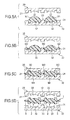
- Figs. 3A-3D show an example of a method for manufacturing the aforementioned lens array 1.
- the lenses 2 and the support 3 are formed integrally by double molding.
- the forming mold has an upper mold 20 and a lower mold 30.
- a plurality of lens forming portions 22 are arranged like a matrix in the same layout as the arrangement of the lenses 2 in the lens array 1.
- the lens forming portions 22 form front surface shapes of the lenses 2.
- a plurality of lens forming portions 32 are arranged like a matrix in the same layout as the arrangement of the lenses 2 in the lens array 1.
- the lens forming portions 32 form back surface shapes of the lenses 2.
- the material of the molds 20 and 30 is selected suitably in accordance with the energy-curing resin material forming the lenses 2 or the support 3.
- thermosetting resin for example, a metal material superior in coefficient of thermal conductivity or a material capable of transmitting infrared rays may be used as the material of the molds.
- ultraviolet-curing resin for example, a material capable of transmitting ultraviolet rays is used as the material of the molds.
- resin curable by electron rays is used as the resin material, a material, capable of transmitting the electron rays is used as the material of the molds.
- a resin material M1 forming the lenses 2 is dripped to each lens forming portion 32 of the lower mold 30.
- a resin material M2 forming the support 3 is supplied onto the molding surface 31 of the lower mold 30 excluding the lens forming portions 32.
- the upper mold 20 is moved down to compress the resin materials M1 and M2 between the molding surface 21 of the upper mold 20 and the molding surface 31 of the lower mold 30.
- the resin materials M1 and M2 are deformed in accordance with the molding surfaces 21 and 31.
- the lenses 2 are formed between the paired lens forming portions 22 and 32 respectively.
- the support 3 is formed between the molding surfaces 21 and 31 excluding the lens forming portions 22 and 32. The lenses 2 and the support 3 are formed integrally in the state where they are bonded with each other.
- the lenses 2 and the support 3 are formed by casting and compression of the resin materials respectively, but they are not limited to this method.
- the lenses 2 may be formed by casting and compression while the support 3 is formed by injection of the resin material into a cavity in the state where the forming molds are closed for forming the lenses 2.
- the lenses 2 produced individually in advance may be inserted while the support 3 is formed by casting and compression or injection.
- it is preferable that formation of the lenses 2 and the support 3 is performed under a vacuum environment in order to prevent bubbles from being mixed into the lenses 2 or the support 3.
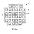
- Fig. 4 shows a modification of the aforementioned lens array 1.
- a hole 12 is formed to penetrate the support 3 in its thickness direction.
- a single hole 12 is provided in a center portion of the support 3, but the number of holes 12 and the positions thereof are not limited.
- a plurality of holes 12 may be provided and distributed all over the support 3.
- Figs. 5A to 5D show an example of a method for manufacturing the lens array 1 shown in Fig. 4 .
- the lenses 2 and the support 3 are formed integrally by double molding.
- the forming mold has an upper mold 20 and a lower mold 30.
- a convex portion 33 is provided in a center portion of a molding surface 31 of the lower mold 30.
- the convex portion 33 protrudes from the molding surface 31 so as to be as high as the thickness of the support 3 in the lens array 1.
- the convex portion 33 abuts against a molding surface 21 of the upper mold 20 when the upper mold 20 and the lower mold 30 are closed.
- a resin material M1 forming the lenses 2 is dripped to each lens forming portion 32 of the lower mold 30.
- a resin material M2 forming the support 3 is supplied onto the molding surface 31 of the lower mold 30 excluding the lens forming portions 32.
- the upper mold 20 is moved down to compress the resin materials M1 and M2 between the molding surface 21 of the upper mold 20 and the molding surface 31 of the lower mold 30.
- the resin materials M1 and M2 are deformed in accordance with the molding surfaces 21 and 31.
- the lenses. 2 are formed between the paired lens forming portions 22 and 32 respectively.
- the support 3 is formed between the molding surfaces 21 and 31 excluding the lens forming portions 22 and 32 and the convex portion 33.
- the lenses 2 and the support 3 are formed integrally in the state where they are bonded with each other.
- a hole 12 penetrating the support 3 in its thickness direction is formed by the convex portion 33 of the lower mold 30.
- the convex portion 33 abutting against the molding surface 21 of the upper mold 20 is provided in the molding surface 31 of the lower mold 30 so that the hole 12 penetrating the support 3 in its thickness direction can be formed in the support 3 by molding the resin material.
- the convex portion 33 is brought into abutment against the molding surface 21 of the upper mold 20, the distance between the molding surface 21 of the upper mold 20 and the molding surface 31 of the lower mold 30 in the periphery of the convex portion 33 can be defined uniquely.
- Distortion may appear in a forming mold due to a load etc. imposed on the forming mold when resin materials are compressed.
- a lens array for mass-producing lens groups of imaging units to be mounted on cellular phones or the like has a wafer-like shape (disc-like shape) whose diameter is, for example, 6 inches, 8 inches or 12 inches as a whole.
- a forming mold for forming the lens array typically has a comparatively large area of a molding surface relative to the thickness thereof. Thus, distortion may appear in the forming mold easily. The distortion in the forming mold leads to a variation in distance between molding surfaces to produce an error in thickness among lenses.
- the convex portion 33 is brought into abutment against the molding surface 21 of the upper mold 20 to uniquely define the distance between the molding surface 21 of the upper mold 20 and the molding surface 31 of the lower mold 30 in the periphery of the convex portion 33.
- the accuracy of the thickness of each lens 2 formed thus can be enhanced to obtain desired optical performance in the lens 2.
- a plurality of convex portions 33 are provided and distributed all over the molding surface 31. That is, a plurality of holes 12 are provided in the support 3 so as to be distributed all over the support 3.
- Fig. 6 shows an example of an element array laminate.
- the element array laminate shown in Fig. 6 is a lens array laminate in which a plurality of lens arrays 1 in Fig. 1 are laminated on one another.
- a lens array laminate 40 is formed by laminating two lens arrays 1a and 1b on each other.
- Each lens array 1a, 1b has a similar configuration to that of the lens array 1 in Fig. 1 .
- a lens group 41 is constituted by a lens 2a belonging to the lens array 1a and a lens 2b belonging to the lens array 2b, which are arrayed in the laminating direction of the lens arrays 1a and 1b.
- the lenses 2a and 2b constituting the lens group 41 are bonded to align their optical axes with each other.
- the lenses 2a and 2b constituting the lens group 41 are bonded by a bonding agent 42 applied to a flange portion 11 of either of the lenses 2a and 2b or flange portions 11 of both the lenses 2a and 2b.
- Fig. 7A shows a state where the lens arrays 1a and 1b have not yet been laminated.
- Fig. 7A shows a case where misalignment appears between the pitch of lenses 2a in the lens array 1a and the pitch of lenses 2b in the lens array 1b. Hence, misalignment also appears between the optical axes of the lenses 2a and 2b constituting the lens group 41.
- the bonding agent 42 is put between the flange portions 1I of the lenses 2a and 2b constituting the lens group 41. Due to the self-alignment effect caused by the surface tension of the bonding agent 42, one lens 2a is moved relatively to the other lens 2b in the pitch direction while suitably expanding/contracting the support 3 belonging to the lens array 1a and the support 3 belonging to the lens array 1b. Thus, the lenses 2a and 2b are aligned with each other. When the bonding agent 42 is cured in that state, the lenses 2a and 2b are bonded in the state where their optical axes are aligned with each other.
- the self-alignment effect of the bonding agent 42 is expressed by the edge (macroscopic shape) of the bonding face of each flange portion 11.
- the self-alignment effect of the bonding agent 42 may be expressed by adjusting the surface texture (microscopic shape) of the bonding face of each flange portion 11 or depositing a film on the bonding face to thereby pattern wettability with the bonding agent 42 on the bonding face.
- the bonding agent 42 is typically contracted as it is cured. In some case, it is considered that a variation in height may appear among the lens groups 41 due to the thickness of the bonding agent 42 which has been cured. Therefore, as shown in Fig. 8 , microscopic spheres 43 which are uniform in particle size may be mixed into the bonding agent 42. When the distance between the bonding surfaces is defined by the diameter of the microscopic spheres 43, the variation in height among the lens groups 41 can be suppressed.
- Fig. 9 shows another modification of the lens array 1 in Fig. 1 , and a laminate thereof.
- a fit convex portion 13 is provided in a flange portion 11 of each lens 2a belonging to a lens array 1a, while a fit concave portion 14 to which the fit convex portion 13 is fitted is provided in a flange portion 11 of each lens 2b belonging to a lens array 1b.
- the lenses 2a and 2b are aligned with each other.
- the lenses 2a and 2b are bonded in the state where their optical axes are aligned.
- the other lens 2b can be positioned in the laminating direction when the fit concave portion 14 is brought into abutment against the fit convex portion 13.
- the variation in height among the lens groups 41 can be suppressed.
- Fig. 10 shows another modification of the lens array 1 in Fig. 1 , and a laminate thereof.
- a fitting face of a fit convex portion 13 provided in a flange portion 11 of each lens 2a belonging to a lens array 1 a and a fitting face of a fit concave portion 14 provided in a flange portion 11 of each lens 2b belonging to a lens array 1b are formed into tapered faces which can be mated with each other.
- the lenses 2a and 2b are aligned with each other so that the lenses 2a and 2b can be bonded in the state where their optical axes are aligned.
- the other lens 2b can be positioned in the laminating direction when the fit concave portion 14 is brought into abutment against the fit convex portion 13.
- a variation in height among the lens groups 41 can be suppressed.
- the fitting faces of the fit convex portion 13 and the fit concave portion 14 are tapered faces, the both can be fitted to each other smoothly.
- Fig. 11 shows another modification of the lens array 1 in Fig. 1 , and a laminate thereof.
- pinching portions 15 for elastically pinching lenses 2b belonging to a lens array 1b are provided in flange portions 11 of lenses 2a belonging to a lens array 1a so as to be arranged in the array direction of the lenses 2a in the lens array 1a.
- Each pinching portion 15 is constituted by a pair of elastic pieces 16 opposed to each other in a row direction which is the array direction of the lenses 2a in the lens array 1a and a pair of elastic pieces 16 opposed to each other in a column direction (only the pair of elastic pieces 16 opposed in the row direction are shown in Fig. 11 ). Holes through which the elastic pieces 16 can be inserted are suitably formed in a support 3 belonging to the lens array 1b
- the elastic pieces 16 are formed out of a material more elastic than the material forming the support 3.
- the elastic pieces 16 are formed integrally with the lenses 2a, for example, by insert molding.
- the support 3 belonging to the lens array 1a and the support 3 belonging to the lens array 1b are expanded/contracted in the row direction and the column direction respectively so that the lenses 2a and 2b can be aligned with each other.
- front end portions of the elastic pieces 16 can be engaged with front edge portions of the flange portions 11 of the lenses 2b so that the lenses 2a and 2b can be locked in the state where their optical axes are aligned with each other.
- a plurality of lens arrays 1 in Fig. 1 (or lens arrays according to a modification thereof) are laminated.
- the lens array 1 in Fig. 1 may be laminated on another element array to form an element array laminate.
- Fig. 12 shows another example of an element array laminate.
- an element array laminate 50 is constituted by the lens array 1 in Fig. 1 and a lens array 53 laminated sequentially on a sensor array 52.
- the sensor array 52 has a wafer 60 formed out of a semiconductor material such as silicon.
- a plurality of solid-state image sensors 61 are formed on the wafer 60.
- the solid-state image sensors 61 are, for example, CCD image sensors, CMOS image sensors, or the like, which are formed as follows. That is, a film forming step, a photolithographic step, an etching step, an impurities adding step, etc. as known well are performed on the wafer 60 repeatedly to form light receiving regions, an insulating film, electrodes, wiring, etc. on the wafer 60.
- the lens array 53 has a plurality of lenses 70 and a substrate portion 71 coupling the lenses 70 with one another.
- the lenses 70 and the substrate portion 71 are formed integrally out of a translucent resin composition.
- the substrate portion 71 is formed into a wafer-like shape having the same size as the wafer 60 of the sensor array 52.
- the same resin composition as the resin composition forming the lenses 2 in the lens array 1 may be used as the resin composition forming the lenses 70 and the substrate portion 71. Accordingly, the substrate portion 71 is higher in rigidity than the support 3 in the lens array 1, but the lenses 70 in the lens array 53 are not coupled flexibly.
- the layout of the solid-state image sensors 61 in the sensor array 52 and the layout of the lenses 70 in the lens array 53 are arranged in the same manner as the layout of the lenses 2 in the lens array 1.
- a lens group 54 is constituted by a lens 2 and a lens 70 arrayed in the laminating direction.
- One imaging unit 55 is constituted by the lens group 54 and a solid-state image sensor 61.
- the lens array 1 and the lens array 53 are first laminated to obtain a lens array laminate 51.
- the support 3 belonging to the lens array 1 is expanded/contracted suitably so that the lenses 2 and the lenses 70 forming the lens groups 54 can be aligned with each other.
- the aforementioned self-alignment of the bonding agent 42 (see Figs. 7A and 7B ), the fit convex portion 13 and the fit concave portion 14 (see Figs. 9 and 10 ) or the pinching portion 15 (see Fig. 11 ) may be used suitably as an alignment portion between each lens 2 and each lens 70.
- the lens array laminate 51 is laminated on the sensor array 52.
- the accuracy required for the alignment between each lens group 54 and each solid-state image sensor 61 is comparatively lower than the accuracy required for the alignment between each lens 2 and each lens 70 constituting each lens group 54. Since the layout of the solid-state image sensors 61 in the sensor array 52 is arranged in the same manner as the layout of the lens groups 54 in the lens array laminate 51, a plurality of imaging units 55 can be formed in a lump when the lens array laminate 51 is laminated on the sensor array 52.
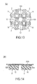
- Fig. 13 shows another example of an element array.
- the element array shown in Fig. 13 is a lens array.
- Members common to the aforementioned lens array 1 are given common reference signs correspondingly, so that description thereof will be omitted or simplified.
- a lens array 101 has a plurality of lenses 2 and a plurality of elastic pieces 103 serving as a support.
- the lenses 2 are arrayed like a matrix.
- the elastic pieces 103 are provided between adjacent ones of the lenses 2 respectively. In the illustrated example, two elastic pieces 103 are provided between the lenses 2 adjacent to each other. However, one may be provided likewise, or three or more may be provided likewise.
- the gap between each lens 2 and lenses 2 around the lens 2 is segmented by the elastic pieces 103 provided in the gap so as to form a plurality of holes 12.
- each elastic piece 103 End portions of each elastic piece 103 are bonded to opposed surfaces of two flange portions 11 of two lenses 2 between which the elastic piece 103 is placed, so that the elastic piece 103 can couple the two lenses 2 with each other.
- the elastic pieces 103 are formed out of a material richer in elasticity (richer in stretchability) than the material forming the lenses 2, so that flexibility can be given to the elastic pieces 103. Further, each elastic piece 103 is formed meandering with respect to a straight line connecting the places where the elastic piece 103 is bonded with the flange portions 11 of two lenses 2 to be coupled. Due to such a shape, flexibility can be further provided. That is, each elastic piece 103 can be deformed from a meandering shape to a straight shape or from a straight shape to a meandering shape so as to displace the lenses 2 in their array directions (row direction and column direction).
- the lens array 101 may be manufactured in the same manufacturing method as the lens array 1 shown in Figs. 5A-5D . Refer to Figs. 5A-5D .
- the convex portions 33 are provided in positions corresponding to the holes 12 respectively.
- the resin material for forming the lenses 2 and the resin material for forming the elastic pieces 103 are cast, compressed, and cured to obtain the lens array 101.
- Each lens 2 is formed between a pair of lens forming portions 22 and 32.
- the elastic pieces 103 are formed between the molding surfaces 21 and 31 excluding the lens forming portions 22 and 32 and the convex portions 33.
- the lenses 2 and the elastic pieces 103 are formed integrally in the state where they are bonded with each other.
- the convex portions 33 for forming the holes 12 are provided in the molding surface 31 of the lower mold 30.
- the distance between the molding surface 21 of the upper mold 20 and the molding surface 31 of the lower mold 30 in the periphery of each convex portion 33 can be defined uniquely. The accuracy of the thickness of each lens 2 formed thus can be enhanced to obtain desired optical performance in the lens 2.
- the aforementioned self-alignment of the bonding agent 42 (see Figs. 7A and 7B ), the fit convex portion 13 and the fit concave portion 14 (see Figs. 9 and 10 ) or the pinching portion 15 (see Fig. 11 ) may be used suitably as an alignment portion between each lens 2 belonging to the lens array 101 and each element belonging to another element array which are arrayed in the laminating direction when the lens array 101 and the other element array are laminated.
- Fig. 14 shows another example of an element array.
- the element array shown in Fig. 14 is a lens array.
- Members common to the aforementioned lens array 1 are given common reference signs correspondingly, so that description thereof will be omitted or simplified.
- a lens array 201 has a plurality of lenses 2 and a sheet member 203 serving as a support.
- the lenses 2 are arrayed like a matrix. Flange portions 11 of the lenses 2 are removably bonded to one surface of the sheet member 203 through a removable adhesive sheet 204 so that the lenses 2 are coupled with one another by the sheet member 203. It is preferably that the adhesive sheet 204 for bonding the lens 2 with the sheet member 203 can be easily removed by heating or irradiation with ultraviolet rays.
- the sheet member 203 is formed out of a material richer in elasticity (richer in stretchability) than the material forming the lenses 2, so that flexibility can be given to the sheet member 203.
- the lenses 2 can be displaced in their array directions (row direction and column direction).
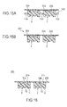
- Fig. 15A and Fig. 15B show an example or a method for manufacturing the lens array 201 in Fig. 14 .
- the lens array 101 shown in Fig. 6 is prepared, and the lenses 2 belonging thereto are bonded to the sheet member 203 through the adhesive sheet 204 in a lump.
- the elastic pieces 103 of the lens array 101 are cut to separate the lenses 2 individually and obtain the lens array 201.
- the lenses 2 are coupled flexibly through the sheet member 203.
- the aforementioned example has been described on the assumption that the lens array 10 shown in Fig. 6 is used, whether or not the lenses 2 are coupled flexibly in the lens array to be bonded to the sheet member 203 is no object as long as the lenses 2 are arrayed and coupled with one another in the same manner.
- the adhesive sheet 204 is released by heating or irradiation with ultraviolet rays so that the sheet member 203 belonging to the lens array 201 can be removed from the lens array 201.
- the aforementioned self-alignment of the bonding agent 42 (see Figs. 7A and 7B ), the fit convex portion 13 and the fit concave portion 14 (see Figs. 9 and 10 ) or the pinching portion 15 (see Fig. 11 ) may be used suitably as an alignment portion between each lens 2 belonging to the lens array 201 and each element belonging to another element array which are arrayed in the laminating direction when the lens array 201 and the other element array are laminated.
- the adhesive sheet 204 is made elastic so that the lenses 2 in their array directions (row direction and column direction) can be displaced due to the elasticity of the adhesive sheet 204.
- a rigid substrate-like member may be used as the sheet member 203.
- Fig. 16 shows a modification of the lens array 201 in Fig. 14 .
- each hole 214 is formed to be large enough to expose the whole of an optical surface 10a of the optical function portion 10.
- the hole 214 may be formed to be large enough to overlap with an outer edge of the optical surface 10a while the sheet member 203 is formed out of a light shielding material or a light shielding paint or the like is applied to the surface of the sheet member 203 so that apertures may be formed by the sheet member 203.
- Figs. 17A-17D show an example of a method for manufacturing the lens array 201 in Fig. 16 .
- the sheet member 203 is inserted into a forming mold to form a plurality of lenses 2 bonded with the sheet member 203.
- the sheet member 203 is applied onto the molding surface 21 of the upper mold 20.
- a resin material, M1 for forming the lenses 2 is dripped to each lens forming portion 32 of the lower mold 30.
- the upper mold 20 is moved down to compress the resin material M1 between the molding surface 21 of the upper mold 20 and the molding surface 31 of the lower mold 30.
- the resin material M1 is deformed in accordance with the molding surfaces 21 and 31.
- Fig. 17D energy is applied to the resin material M1 to cure the resin material M1 and obtain the lens array 201.
- the lenses 2 are formed between the paired lens forming portions 22 and 32 respectively.
- the lenses 2 and the sheet member 203 are formed in the state where they are bonded with each other.
- the holes 214 for exposing the optical function portions 10 of the lenses 2 are formed in the sheet member 203 so that the lens array 201 can be laminated with another element array without removing the sheet member 203 from the lens array 201.
- Fig. 18 shows another example of an element array, and a laminate thereof.
- the element array shown in Fig. 18 is a microchemical chip array in which a plurality of microchemical chips for medical diagnosis are arrayed.
- the element array laminate shown in Fig. 18 is a microchemical chip array laminate constituted by a plurality of microchemical chip arrays built into layers.
- a microchemical chip array laminate 301 is constituted by two microchemical chip arrays 302a and 302b built into layers.
- the microchemical chip array 302a has a plurality of microchemical chips 310a and a plurality of elastic pieces 311 serving as a support.
- the microchemical chip array 302b has a plurality of microchemical chips 310b and a plurality of elastic pieces 311 serving as a support.
- the configuration of each part is basically common between the microchemical chip array 302a and the microchemical chip array 302b. Therefore, the following description will be made on only the microchemical chip array 302a.
- the microchemical chips 310a are arrayed like a matrix in the illustrated example.
- the layout of the microchemical chips 310a is not limited to the matrix, but may be a radial or concentrically annular array, another two-dimensional array or a one-dimensional array.
- Each elastic piece 311 is provided between adjacent ones of the microchemical chips 310a. End portions of the elastic piece 311 are bonded to opposed surfaces of two microchemical chips 310a between which the elastic piece 311 is placed, so that the elastic piece 311 couples the two microchemical chips 310a with each other.
- the elastic pieces 311 are formed out of a material richer in elasticity (richer in stretchability) than the material forming the microchemical chips 310a, so that flexibility can be given to the elastic pieces 311.
- the microchemical chips 310a can be displaced in their array directions (row direction and column direction).
- Fig. 19 shows an enlarged view of the microchemical chips 310a and 310b in Fig. 18 .
- microscopic channels 312 where sample liquid should be circulated are formed in the microchemical chips 310a and 310b.
- the channels 312 formed in the microchemical chips 310a and 310b respectively communicate with each other when the microchemical chips 310a and 310b are laminated.
- Each channel 312 is typically formed to have a width of several ⁇ m to several hundreds of ⁇ m.
- the accuracy required for alignment between the microchemical chips 310a and 310b is typically not larger than several ⁇ m.
- Fig. 20 shows a state where the microchemical chips 310a and 310b in Fig. 18 are laminated while the centers of the microchemical chips 310a and 310b are misaligned with each other.
- a step portion 313 occurs at the place where the channels 312 of the microchemical chips 310a and 310b are connected.
- sample liquid is circulated through the step portion 313, there may arise a problem that an air pool is formed and a sample liquid pool is also formed to increase the amount of sample liquid required for diagnosis.
- the microchemical chips 310a and 310b When the microchemical chips 310a and 310b are coupled with each other flexibly through the elastic pieces 311, it is possible to move one microchemical chip 310a in the pitch direction relatively to the other microchemical chip 310b while suitably expanding/contracting the elastic pieces 311. Thus, the microchemical chips 310a and 310b can be aligned so that the aforementioned problem can be solved.
- the aforementioned self-alignment of the bonding agent 42 (see Figs. 7A and 7B ), the fit convex portion 13 and the fit concave portion 14 (see Figs. 9 and 10 ) or the pinching portion 15 (see Fig. 11 ) may be used suitably as an alignment portion between the microchemical chips 310a and 310b.
- an element array disclosed in the specification includes: a plurality of elements which are arrayed one-dimensionally or two-dimensionally, and a flexible support which is formed out of a material richer in elasticity than a material forming the elements; in which: the elements are coupled with one another through the support.
- the support is formed to fill a gap between each of the elements and another element around the element.
- At least one hole penetrating the support in a thickness direction thereof is formed in the support.
- the support includes a plurality of elastic pieces provided between adjacent ones of the elements respectively; and each of the elastic pieces is bonded to two of the elements between which the elastic piece is placed.
- the support is a sheet member; and each of the elements is bonded to one surface of the sheet member.
- each of the elements is removably bonded to the sheet member.
- the support is an adhesive sheet which is bonded to one surface of a substrate; and each of the elements is removably bonded to the adhesive sheet.
- each of the elements has a joint portion to be bonded to another element belonging to another element array and laid on the element; and an alignment portion for alignment with the other element is provided in the joint portion.
- the alignment portion is a fit portion which is fitted to the other element.
- a fit surface of the fit portion is a tapered surface.
- the alignment portion is a pinching portion which pinches the other element elastically in an array direction of the elements.
- the alignment portion is a pattern formed in a joint surface of the joint portion; and the pattern controls wettability to a bonding agent to express a self-alignment effect of the bonding agent.
- an element array laminate disclosed in the specification includes a plurality of element arrays built into layers and each having a plurality of elements arrayed one-dimensionally or two-dimensionally, each group of the elements arrayed in a laminating direction being aligned with one another, in which at least one layer of the element arrays is any one of the element arrays described above.
- the invention is useful when a plurality of structures each consisting of a plurality of elements built into layers are formed in a lump.
Landscapes
- Physics & Mathematics (AREA)
- Engineering & Computer Science (AREA)
- General Physics & Mathematics (AREA)
- Optics & Photonics (AREA)
- Manufacturing & Machinery (AREA)
- Health & Medical Sciences (AREA)
- Ophthalmology & Optometry (AREA)
- Mechanical Engineering (AREA)
- Lens Barrels (AREA)
- Mounting And Adjusting Of Optical Elements (AREA)
- Casting Or Compression Moulding Of Plastics Or The Like (AREA)
Abstract

Description
- The present invention relates to an element array and an element array laminate.
- In recent years, a small-size and low-profile imaging unit has been mounted on a portable terminal of an electronic device, such as a cellular phone or a PDA (Personal Digital Assistant). Such an imaging unit is generally provided with a solid-state image sensor such as a CCD (Charge Coupled Device) image sensor or a CMOS (Complementary Metal-Oxide Semiconductor) image sensor, and a lens group for forming an image in a light receiving area of the solid-state image sensor.
- With reduction in size and profile of portable terminals and wide use of the portable terminals, there has been a demand for further reduction in the size and profile of imaging units mounted on the portable terminals while the productivity thereof is also requested. In response to such a request, there has been proposed a technique for mass-producing modules of a lens array laminate in such a manner that a large number of lenses and coupling portions for coupling those lenses with one another are integrally formed out of a photocuring or thermosetting resin material to thereby constitute each lens array, the lens arrays are put into a plurality of layers to form a lens array laminate, and the lens array laminate is divided into a plurality of modules each including a group of lenses arrayed in the laminating direction (see Patent Literature 1 (
WO 081533102 - In an imaging unit mounted on a cellular phone or the like, accuracy of alignment of µm order is typically required in a group of lenses. The accuracy of alignment in the group of lenses depends on the pitch accuracy of the lenses in each lens array. In the technique disclosed in
Patent Literature 1, for example, an error in pitch among lenses may appear due to influence of variation in light intensity or temperature during curing of a resin material. In addition, an error in pitch among lens forming surfaces of molds for molding the resin material or deformation of a lens array caused by the release of the lens array from the mold may cause the error in pitch among the lenses. Due to a series of such error factors, it has been difficult to suppress the error in pitch among the lenses down to the order of µm in the whole lens array according to the technique disclosed inPatent Literature 1. - To solve the foregoing problem, in a lens array in which a large number of lenses and a coupling portion coupling the lenses with one another are formed integrally, there has been proposed a technique for forming slits in the coupling portion to give flexibility to the coupling portion so that the error in pitch among the lenses can be absorbed by deformation of the coupling portion (see Patent Literature 2 (
JP-A-2004-226872 - Only by forming slits in a coupling portion formed integrally out of the same material as lenses, enough flexibility cannot be given to the coupling portion. Thus, there has been a fear that the error in pitch among the lenses cannot be absorbed satisfactorily.
- The present invention has been developed in consideration of the aforementioned circumstances. An object of the invention is to provide an element array in which an error in pitch among elements in the element array can be absorbed surely in a step of laminating a plurality of element arrays so that each group of the elements arrayed in the laminating direction can be aligned with high accuracy.
- An element array includes a plurality of elements which are arrayed one-dimensionally or two-dimensionally, and a flexible support which is formed out of a material richer in elasticity than a material forming the elements; in which: the elements are coupled with one another through the support.
- According to the invention, a support is formed out of a material richer in elasticity than a material forming elements so that flexibility sufficient enough to absorb an error in pitch among the elements can be secured in the support. Thus, the error in pitch among the elements can be absorbed surely in a step of laminating a plurality of element arrays, so that an element array laminate in which each group of elements arrayed in the laminating direction are aligned with high accuracy can be obtained.
-
-
Fig. 1 is a view showing an example of an element array for explaining an embodiment of the invention. -
Fig. 2 is a view showing the element array inFig. 1 by section taken on line II-II. -
Figs. 3A to 3D are views showing an example of a method for manufacturing the element array inFig. 1 . -
Fig. 4 is a view showing a modification of the element array inFig. 1 . -
Figs. 5A to 5D are views showing an example of a method for manufacturing the element array inFig. 4 . -
Fig. 6 is a view showing an example of an element array laminate for explaining the embodiment of the invention. -
Fig. 7A is a view showing a state where a plurality of element arrays forming the element array laminate inFig. 6 have not yet been laminated, andFig. 7B is a view showing a state where the element arrays have been laminated to form the element array laminate. -
Fig. 8 is an enlarged view of a portion surrounded by a dotted circle VIII in the element array laminate inFig. 7B . -
Fig. 9 is a view showing a modification of the element array inFig. 1 , and a laminate thereof. -
Fig. 10 is a view showing another modification of the element array inFig. 1 , and a laminate thereof. -
Fig. 11 is a view showing another modification of the element array inFig. 1 , and a laminate thereof. -
Fig. 12 is a view showing another example of an element array laminate for explaining the embodiment of the invention. -
Fig. 13 is a view showing another example of an element array for explaining the embodiment of the invention. -
Fig. 14 is a view showing another example of an element array for explaining the embodiment of the invention. -
Figs. 15A and 15B are views showing an example of a method for manufacturing the element array inFig. 14 . -
Fig. 16 is a view showing a modification of the element array inFig. 14 . -
Figs. 17A to 17D are views showing an example of a method for manufacturing the element array inFig. 16 . -
Fig. 18 is a view showing another example of an element array for explaining the embodiment of the invention, and a laminate thereof. - Fig. 29 is an enlarged view showing a portion surrounded by a dotted circle XIX in the element array laminate in
Fig. 18 . -
Fig. 20 is a view sectionally showing an element group included in the element array laminate inFig. 18 , in which the centers of a plurality of elements forming the element group are misaligned with each other, - 1,1a,1b
- lens array (element array)
- 2
- lens (element)
- 3
- support
- 10
- optical function portion
- 11
- flange portion
- 12
- hole
- 13
- fit convex portion
- 14
- fit concave portion
- 15
- pinching portion
- 16
- elastic piece
- 20
- upper mold
- 21
- molding surface
- 22
- lens forming portion
- 30
- lower mold
- 31
- molding surface
- 32
- lens forming portion
- 40
- lens array laminate (element array laminate)
- 41
- lens group
- 42
- bonding agent
- 43
- microscopic sphere
- 50
- element array laminate
- 51
- lens array laminate
- 52
- sensor array
- 53
- lens array
- 54
- lens group
- 55
- imaging unit
- 60
- wafer
- 61
- solid-state image sensor
- 70
- lens
- 71
- substrate portion
- 101
- lens array
- 103
- elastic piece (support)
- 201
- lens array
- 203
- sheet member (support)
- 204
- adhesive sheet
- 214
- hole
- 301
- microchemical chip array laminate (element array laminate)
- 302a,302b
- microchemical chip array (element array)
- 3110a,310b
- microchemical chip (element)
- 311
- elastic piece (support)
- 312
- channel
- 313
- step portion
-
Figs. 1 and 2 show an example of an element array. The element array shown inFigs. 1 and 2 is a lens array. - As shown in
Figs. 1 and 2 , alens array 1 has a plurality oflenses 2 and asupport 3. - The
lenses 2 are arrayed in a matrix in the illustrated example. The layout of thelenses 2 is not limited to the matrix, but may be radial or concentrically annular array, another two-dimensional array or a one-dimensional array. - Predetermined
optical faces lens 2. Although both theoptical faces - In addition, each
lens 2 has aflange portion 11. Theflange portion 11 is formed into a frame-like shape surrounding an outer circumference of anoptical function portion 10 put between theoptical faces optical function portion 10 is received in theflange portion 11. Although the outer shape of theflange portion 11 in plan view is rectangular in the illustrated example, the outer shape of theflange portion 11 may be a circle, a polygon or the like. - The
support 3 is formed to fill a gap between eachlens 2 andother lenses 2 around thelens 2. Thesupport 3 has a net-like (lattice-like) shape as a whole. Thesupport 3 is bonded to circumferential faces of theflange portions 11 of thelenses 2 so as to couple thelenses 2 with one another. - The
support 3 is formed out of a material richer in elasticity (richer in stretchability) than the material forming thelenses 2, so that flexibility can be given to thesupport 3. Thus, thelenses 2 can be displaced in their array directions (row direction and column direction). When the width of eachlens 2 is 1, the distance between adjacent two of thelenses 2, that is, the width of thesupport 3 disposed between thoselenses 2 is typically expressed as 1/4 to 1/5. It is therefore preferable that the material forming thesupport 3 is 4 to 5 times as stretchable as the material forming thelenses 2. - The
lenses 2 are formed out of a translucent resin composition. For example, an energy-curing resin composition can be suitably used as the resin composition. The energy-curing resin composition may be either a resin composition that can be cured by heat or a resin composition that can be cured by irradiation with active energy rays (e.g. irradiation with ultraviolet rays or electron rays). - It is preferable that the resin composition forming the
lenses 2 has moderate fluidity before curing from the point of view of moldability including suitability to transfer the shape of a mold. Specifically, a resin composition which is a liquid at a normal temperature and whose viscosity is about 1,000 to 50,000 mPa·s is preferable. - It is also preferable that the resin composition forming the
lenses 2 has enough heat resistance not to be thermally deformed even in a reflow step after curing. In this point of view, the glass transition temperature of the cured composition is preferably not lower than 200°C, more preferably not lower than 250°C, particularly preferably not lower than 300°C. In order to give such a high heat resistance to the resin composition, it is necessary to put molecular-level restraints on the motility of the resin composition. Examples of effective methods include (1) a method for increasing crosslink density per unit volume, (2) a method using resin with a rigid ring structure (such as resin with an alicyclic structure of cyclohexane, norbornane, tetracyclododecane, etc., an aromatic ring structure of benzene, naphthalene, etc., a cardo structure of 9,9-biphenyl fluorene etc., a spiro structure of spirobiindan etc., specifically, resin e.g. disclosed inJP-A-9-137043 JP-A-10-67970 JP-A-2003-55316 JP-A-2007-334018 JP-A-2007-238883 JP-A-5-209027 JP-A-10-298265 - In addition, it is preferable that the resin composition forming the
lenses 2 is a resin composition with a low degree of volume shrinkage due to curing reaction from the point of view of accuracy in shape transfer. The degree of cure shrinkage of the resin composition is preferably not higher than 10%, more preferably not higher than 5%, particularly preferably not higher than 3%. Examples of low-cure-shrinkage resin compositions include (1) a resin composition containing a high-molecular curing agent (prepolymer etc.) (e.g. disclosed inJP-A-2001-19740 JP-A-2004-302293 JP-A-2007-211247 JP-A-6-298883 JP-A-2001-247793 JP-A-2006-225434 JP-A-2004-210932 JP-A-8-134405 JP-A-2002-105110 JP-A-7-62065 JP-A-2003-20334 JP-A-2005-15666 JP-A-9-137043 JP-A-2006-131868 JP-A-2004-2719 JP-A-2008-238417 - In addition, a mixture of resins having at least two different kinds of high and low Abbe numbers is desirable as the resin composition forming the
lenses 2. The Abbe number (vd) of the high Abbe-number resin is preferably not lower than 50, more preferably not lower than 55, particularly preferably not lower than 60. The refractive index (nd) is preferably not lower than 1.52, more preferably not lower than 1.55, particularly preferably not lower than 1.57. Preferable examples of such resins include aliphatic resins. Of them, particularly a resin having an alicyclic structure (e.g. resin having a ring structure such as cyclohexane, narbornane, adamantane, tricyclodecane, tetracyclodecane. etc., and specifically, resin e.g. disclosed inJP-A-10-152551 JP-A-2002-212500 JP-A-2003-20334 JP-A-2004-210932 JP-A-2006-199790 JP-A-2007-2144 JP-A-2007-284650 JP-A-2008-105999 JP-A-60-38411 JP-A-10-67977 JP-A-2002-47335 JP-A-2003-238884 JP-A-2004-83855 JP-A-2005-325331 JP-A-2007-238883 WO 2006/095610 , Japanese Patent No.2537540 - In addition, it is preferable that inorganic particulates are dispersed into the matrix in the resin composition forming the
lenses 2 in order to enhance the refractive index or adjust the Abbe number. Examples of the inorganic particulates include oxide particulates, sulfide particulates, selenide particulates, and telluride particulates. More specifically, those examples include particulates of zirconium oxide, titanium oxide, zinc oxide, tin oxide, niobium oxide, cerium oxide, aluminum oxide, lanthanum oxide, yttrium oxide, zinc sulfide, etc. Particularly in the aforementioned high Abbe-number resin, it is preferable that particulates of lanthanum oxide, aluminum oxide, zirconium oxide, etc. are dispersed. In the low Abbe-number resin, it is preferable that particulates of titanium oxide, tin oxide, zirconium oxide etc. are dispersed. One kind of inorganic particulates may be used alone or two or more kinds of inorganic particulates may be used together. In addition, the inorganic particulates may be a composite of a plurality of components. In addition, for the sake of various objects such as reduction in photo-catalytic activity or reduction in water absorption, the inorganic particulates may be doped with a different kind of metal, the surface layer of the inorganic particulates may be coated with oxide of a different kind of metal such as silica or alumina, or the surface of the inorganic particulates may be modified with a silane coupling agent, a titanate coupling agent, a dispersing agent containing organic acid (carboxylic acids, sulfonic acids, phosphoric acids, phosphonic acids, etc.) or an organic acid group, etc. The number average particle size of the inorganic particulates may be normally set at about 1 nm to 1,000 nm. When the particle size is too small, the physical properties may change. When the particle size is too large, the influence of Rayleigh scattering may become conspicuous. Therefore, the particle size is preferably in a range of from 1 nm to 15 nm, more preferably in a range of from 2 nm to 10 nm, particularly preferably in a range of from 3 nm to 7 nm. In addition, it is desirable that the particle size distribution of the inorganic particulates is narrower. Such monodisperse particles may be defined in various ways. For example, a numeric range defined as disclosed inJP-A-2006-160992 - To disperse the particulates into the resin composition uniformly, it is desirable to disperse the particulates suitably by use of, for example, a dispersing agent containing functional groups with reactivity to resin monomers forming the matrix (e.g. disclosed in Example of
JP-A-2007-238884 JP-A-2007-211164 JP-A-2007-238929 JP-A-2007-238930 - In addition, additives including a well-known mold release agent such as a silicon-based agent, a fluorinated agent or a long-chain alkyl-group containing compound, an antioxidant such as hindered phenol, etc. may be suitably blended with the resin composition forming the
lenses 2. - In addition, a curing catalyst or initiator may be blended with the resin composition forming the
lenses 2 if necessary. Specifically, a compound for accelerating curing reaction (radical polymerization or ionic polymerization) due to action of heat or active energy rays, for example, disclosed inJP-A-2005-92099 - The resin composition forming the
lenses 2 can be manufactured by suitably blending the aforementioned components. On this occasion, a solvent does not have to be added separately when low molecular weight monomer (reactive diluent) etc. in a liquid state can dissolve the other components. Otherwise the curing resin composition can be manufactured by dissolving each constituent component by use of a solvent. The solvent which can be used in the curing resin composition is not limited particularly but can be selected suitably as long as the composition can be dissolved or dispersed uniformly without being precipitated. Specifically, examples of such solvents include ketones (e.g. acetone, methyl ethyl ketone, methyl isobutyl ketone, etc.), esters (e.g. ethyl acetate, butyl acetate, etc.), ethers (e.g. tetrahydrofuran, 1,4-dioxane, etc.), alcohols (e.g. methanol, ethanol, isopropyl alcohol, butanol, ethylene glycol, etc.), aromatic hydrocarbons (e.g. toluene, xylene, etc.), water, etc. When the curing composition contains a solvent, it is preferable that the transfer operation of a mold shape is performed after the solvent is dried. - The material forming the
support 3 is not limited particularly as long as it is a material richer in elasticity than the aforementioned material forming thelenses 2. For example, a material in which a filler of a heat-resistant raw material such as silica or polyimide is kneaded in an olefin-based resin may be used. -
Figs. 3A-3D show an example of a method for manufacturing theaforementioned lens array 1. In the example shown inFigs. 3A-3D , thelenses 2 and thesupport 3 are formed integrally by double molding. - First, a forming mold will be described. The forming mold has an
upper mold 20 and alower mold 30. In amolding surface 21 of theupper mold 20, a plurality oflens forming portions 22 are arranged like a matrix in the same layout as the arrangement of thelenses 2 in thelens array 1. Thelens forming portions 22 form front surface shapes of thelenses 2. In amolding surface 31 of thelower mold 30, a plurality oflens forming portions 32 are arranged like a matrix in the same layout as the arrangement of thelenses 2 in thelens array 1. Thelens forming portions 32 form back surface shapes of thelenses 2. - The material of the
molds lenses 2 or thesupport 3. When thermosetting resin is used as the resin material, for example, a metal material superior in coefficient of thermal conductivity or a material capable of transmitting infrared rays may be used as the material of the molds. On the other hand, when ultraviolet-curing resin is used as the resin material, for example, a material capable of transmitting ultraviolet rays is used as the material of the molds. When resin curable by electron rays is used as the resin material, a material, capable of transmitting the electron rays is used as the material of the molds. - As shown in
Fig. 3A , a resin material M1 forming thelenses 2 is dripped to eachlens forming portion 32 of thelower mold 30. - Next, as shown in
Fig. 3B , a resin material M2 forming thesupport 3 is supplied onto themolding surface 31 of thelower mold 30 excluding thelens forming portions 32. - Next, as shown in
Fig. 3C , theupper mold 20 is moved down to compress the resin materials M1 and M2 between themolding surface 21 of theupper mold 20 and themolding surface 31 of thelower mold 30. Thus, the resin materials M1 and M2 are deformed in accordance with the molding surfaces 21 and 31. - Next, as shown in
Fig. 3D , energy is applied to the resin materials M1 and M2 to cure the resin materials M1 and M2 and obtain thelens array 1. Thelenses 2 are formed between the pairedlens forming portions support 3 is formed between the molding surfaces 21 and 31 excluding thelens forming portions lenses 2 and thesupport 3 are formed integrally in the state where they are bonded with each other. - In the aforementioned example, the
lenses 2 and thesupport 3 are formed by casting and compression of the resin materials respectively, but they are not limited to this method. For example, thelenses 2 may be formed by casting and compression while thesupport 3 is formed by injection of the resin material into a cavity in the state where the forming molds are closed for forming thelenses 2. Alternatively, thelenses 2 produced individually in advance may be inserted while thesupport 3 is formed by casting and compression or injection. In any case, it is preferable that formation of thelenses 2 and thesupport 3 is performed under a vacuum environment in order to prevent bubbles from being mixed into thelenses 2 or thesupport 3. -
Fig. 4 shows a modification of theaforementioned lens array 1. - In the
lens array 1 shown inFig. 4 , ahole 12 is formed to penetrate thesupport 3 in its thickness direction. In the illustrated example, asingle hole 12 is provided in a center portion of thesupport 3, but the number ofholes 12 and the positions thereof are not limited. For example, a plurality ofholes 12 may be provided and distributed all over thesupport 3. -
Figs. 5A to 5D show an example of a method for manufacturing thelens array 1 shown inFig. 4 . In the example shown inFigs. 5A to 5D , thelenses 2 and thesupport 3 are formed integrally by double molding. - First, a forming mold will be described. The forming mold has an
upper mold 20 and alower mold 30. Aconvex portion 33 is provided in a center portion of amolding surface 31 of thelower mold 30. Theconvex portion 33 protrudes from themolding surface 31 so as to be as high as the thickness of thesupport 3 in thelens array 1. Theconvex portion 33 abuts against amolding surface 21 of theupper mold 20 when theupper mold 20 and thelower mold 30 are closed. - As shown in
Fig. 5A , a resin material M1 forming thelenses 2 is dripped to eachlens forming portion 32 of thelower mold 30. - Next, as shown in
Fig. 5B , a resin material M2 forming thesupport 3 is supplied onto themolding surface 31 of thelower mold 30 excluding thelens forming portions 32. - Next, as shown in
Fig. 5C , theupper mold 20 is moved down to compress the resin materials M1 and M2 between themolding surface 21 of theupper mold 20 and themolding surface 31 of thelower mold 30. Thus, the resin materials M1 and M2 are deformed in accordance with the molding surfaces 21 and 31. - Next, as shown in
Fig. 5D , energy is applied to the resin materials M1 and M2 to cure the resin materials M1 and M2 and obtain thelens array 1. The lenses. 2 are formed between the pairedlens forming portions support 3 is formed between the molding surfaces 21 and 31 excluding thelens forming portions convex portion 33. Thelenses 2 and thesupport 3 are formed integrally in the state where they are bonded with each other. In the center portion of thesupport 3, ahole 12 penetrating thesupport 3 in its thickness direction is formed by theconvex portion 33 of thelower mold 30. - In this manner, the
convex portion 33 abutting against themolding surface 21 of theupper mold 20 is provided in themolding surface 31 of thelower mold 30 so that thehole 12 penetrating thesupport 3 in its thickness direction can be formed in thesupport 3 by molding the resin material. When theconvex portion 33 is brought into abutment against themolding surface 21 of theupper mold 20, the distance between themolding surface 21 of theupper mold 20 and themolding surface 31 of thelower mold 30 in the periphery of theconvex portion 33 can be defined uniquely. - Distortion may appear in a forming mold due to a load etc. imposed on the forming mold when resin materials are compressed. Particularly a lens array for mass-producing lens groups of imaging units to be mounted on cellular phones or the like has a wafer-like shape (disc-like shape) whose diameter is, for example, 6 inches, 8 inches or 12 inches as a whole. A forming mold for forming the lens array typically has a comparatively large area of a molding surface relative to the thickness thereof. Thus, distortion may appear in the forming mold easily. The distortion in the forming mold leads to a variation in distance between molding surfaces to produce an error in thickness among lenses.
- In the aforementioned manner, the
convex portion 33 is brought into abutment against themolding surface 21 of theupper mold 20 to uniquely define the distance between themolding surface 21 of theupper mold 20 and themolding surface 31 of thelower mold 30 in the periphery of theconvex portion 33. The accuracy of the thickness of eachlens 2 formed thus can be enhanced to obtain desired optical performance in thelens 2. Preferably, a plurality ofconvex portions 33 are provided and distributed all over themolding surface 31. That is, a plurality ofholes 12 are provided in thesupport 3 so as to be distributed all over thesupport 3. -
Fig. 6 shows an example of an element array laminate. The element array laminate shown inFig. 6 is a lens array laminate in which a plurality oflens arrays 1 inFig. 1 are laminated on one another. - As shown in
Fig. 6 , alens array laminate 40 is formed by laminating twolens arrays lens array lens array 1 inFig. 1 . - A
lens group 41 is constituted by alens 2a belonging to thelens array 1a and alens 2b belonging to thelens array 2b, which are arrayed in the laminating direction of thelens arrays lenses lens group 41 are bonded to align their optical axes with each other. Thelenses lens group 41 are bonded by abonding agent 42 applied to aflange portion 11 of either of thelenses flange portions 11 of both thelenses -
Fig. 7A shows a state where thelens arrays Fig. 7A shows a case where misalignment appears between the pitch oflenses 2a in thelens array 1a and the pitch oflenses 2b in thelens array 1b. Hence, misalignment also appears between the optical axes of thelenses lens group 41. - As shown in
Fig. 7B , as thelens arrays bonding agent 42 is put between the flange portions 1I of thelenses lens group 41. Due to the self-alignment effect caused by the surface tension of thebonding agent 42, onelens 2a is moved relatively to theother lens 2b in the pitch direction while suitably expanding/contracting thesupport 3 belonging to thelens array 1a and thesupport 3 belonging to thelens array 1b. Thus, thelenses bonding agent 42 is cured in that state, thelenses - In the example shown in
Fig. 7B , the self-alignment effect of thebonding agent 42 is expressed by the edge (macroscopic shape) of the bonding face of eachflange portion 11. Alternatively, the self-alignment effect of thebonding agent 42 may be expressed by adjusting the surface texture (microscopic shape) of the bonding face of eachflange portion 11 or depositing a film on the bonding face to thereby pattern wettability with thebonding agent 42 on the bonding face. - The
bonding agent 42 is typically contracted as it is cured. In some case, it is considered that a variation in height may appear among thelens groups 41 due to the thickness of thebonding agent 42 which has been cured. Therefore, as shown inFig. 8 ,microscopic spheres 43 which are uniform in particle size may be mixed into thebonding agent 42. When the distance between the bonding surfaces is defined by the diameter of themicroscopic spheres 43, the variation in height among thelens groups 41 can be suppressed. -
Fig. 9 shows another modification of thelens array 1 inFig. 1 , and a laminate thereof. - In a
lens array laminate 40 shown inFig. 9 , a fitconvex portion 13 is provided in aflange portion 11 of eachlens 2a belonging to alens array 1a, while a fitconcave portion 14 to which the fitconvex portion 13 is fitted is provided in aflange portion 11 of eachlens 2b belonging to alens array 1b. - When the fit
convex portion 13 and the fitconcave portion 14 are fitted to each other, thelenses lenses lens 2a, theother lens 2b can be positioned in the laminating direction when the fitconcave portion 14 is brought into abutment against the fitconvex portion 13. Thus, the variation in height among thelens groups 41 can be suppressed. -
Fig. 10 shows another modification of thelens array 1 inFig. 1 , and a laminate thereof. - In a
lens array laminate 40 shown inFig. 10 , a fitting face of a fitconvex portion 13 provided in aflange portion 11 of eachlens 2a belonging to alens array 1 a and a fitting face of a fitconcave portion 14 provided in aflange portion 11 of eachlens 2b belonging to alens array 1b are formed into tapered faces which can be mated with each other. - When the fit
convex portion 13 and the fitconcave portion 14 are fit to each other, thelenses lenses lens 2a, theother lens 2b can be positioned in the laminating direction when the fitconcave portion 14 is brought into abutment against the fitconvex portion 13. Thus, a variation in height among thelens groups 41 can be suppressed. Further, since the fitting faces of the fitconvex portion 13 and the fitconcave portion 14 are tapered faces, the both can be fitted to each other smoothly. -
Fig. 11 shows another modification of thelens array 1 inFig. 1 , and a laminate thereof. - In a
lens array laminate 40 shown inFig. 11 , pinchingportions 15 for elastically pinchinglenses 2b belonging to alens array 1b are provided inflange portions 11 oflenses 2a belonging to alens array 1a so as to be arranged in the array direction of thelenses 2a in thelens array 1a. - Each pinching
portion 15 is constituted by a pair ofelastic pieces 16 opposed to each other in a row direction which is the array direction of thelenses 2a in thelens array 1a and a pair ofelastic pieces 16 opposed to each other in a column direction (only the pair ofelastic pieces 16 opposed in the row direction are shown inFig. 11 ). Holes through which theelastic pieces 16 can be inserted are suitably formed in asupport 3 belonging to thelens array 1b - The
elastic pieces 16 are formed out of a material more elastic than the material forming thesupport 3. Theelastic pieces 16 are formed integrally with thelenses 2a, for example, by insert molding. As the pair ofelastic pieces 16 opposed in the row direction and the pair ofelastic pieces 16 opposed in the column direction pinch thelenses 2b elastically in the row direction and the column direction, thesupport 3 belonging to thelens array 1a and thesupport 3 belonging to thelens array 1b are expanded/contracted in the row direction and the column direction respectively so that thelenses elastic pieces 16 can be engaged with front edge portions of theflange portions 11 of thelenses 2b so that thelenses - In each of the aforementioned examples of element array laminates, a plurality of
lens arrays 1 inFig. 1 (or lens arrays according to a modification thereof) are laminated. However, thelens array 1 inFig. 1 may be laminated on another element array to form an element array laminate. -
Fig. 12 shows another example of an element array laminate. - As shown in
Fig. 12 , anelement array laminate 50 is constituted by thelens array 1 inFig. 1 and alens array 53 laminated sequentially on asensor array 52. - The
sensor array 52 has awafer 60 formed out of a semiconductor material such as silicon. A plurality of solid-state image sensors 61 are formed on thewafer 60. The solid-state image sensors 61 are, for example, CCD image sensors, CMOS image sensors, or the like, which are formed as follows. That is, a film forming step, a photolithographic step, an etching step, an impurities adding step, etc. as known well are performed on thewafer 60 repeatedly to form light receiving regions, an insulating film, electrodes, wiring, etc. on thewafer 60. - The
lens array 53 has a plurality oflenses 70 and asubstrate portion 71 coupling thelenses 70 with one another. Thelenses 70 and thesubstrate portion 71 are formed integrally out of a translucent resin composition. Thesubstrate portion 71 is formed into a wafer-like shape having the same size as thewafer 60 of thesensor array 52. For example, the same resin composition as the resin composition forming thelenses 2 in thelens array 1 may be used as the resin composition forming thelenses 70 and thesubstrate portion 71. Accordingly, thesubstrate portion 71 is higher in rigidity than thesupport 3 in thelens array 1, but thelenses 70 in thelens array 53 are not coupled flexibly. - The layout of the solid-
state image sensors 61 in thesensor array 52 and the layout of thelenses 70 in thelens array 53 are arranged in the same manner as the layout of thelenses 2 in thelens array 1. Alens group 54 is constituted by alens 2 and alens 70 arrayed in the laminating direction. Oneimaging unit 55 is constituted by thelens group 54 and a solid-state image sensor 61. - To laminate the
lens array 1, thesensor array 52 and thelens array 53 to form theelement array laminate 50, thelens array 1 and thelens array 53 are first laminated to obtain alens array laminate 51. On that occasion, thesupport 3 belonging to thelens array 1 is expanded/contracted suitably so that thelenses 2 and thelenses 70 forming thelens groups 54 can be aligned with each other. The aforementioned self-alignment of the bonding agent 42 (seeFigs. 7A and 7B ), the fitconvex portion 13 and the fit concave portion 14 (seeFigs. 9 and10 ) or the pinching portion 15 (seeFig. 11 ) may be used suitably as an alignment portion between eachlens 2 and eachlens 70. - Next, the
lens array laminate 51 is laminated on thesensor array 52. The accuracy required for the alignment between eachlens group 54 and each solid-state image sensor 61 is comparatively lower than the accuracy required for the alignment between eachlens 2 and eachlens 70 constituting eachlens group 54. Since the layout of the solid-state image sensors 61 in thesensor array 52 is arranged in the same manner as the layout of thelens groups 54 in thelens array laminate 51, a plurality ofimaging units 55 can be formed in a lump when thelens array laminate 51 is laminated on thesensor array 52. -
Fig. 13 shows another example of an element array. The element array shown inFig. 13 is a lens array. Members common to theaforementioned lens array 1 are given common reference signs correspondingly, so that description thereof will be omitted or simplified. - As shown in
Fig. 13 , alens array 101 has a plurality oflenses 2 and a plurality ofelastic pieces 103 serving as a support. - The
lenses 2 are arrayed like a matrix. - The
elastic pieces 103 are provided between adjacent ones of thelenses 2 respectively. In the illustrated example, twoelastic pieces 103 are provided between thelenses 2 adjacent to each other. However, one may be provided likewise, or three or more may be provided likewise. The gap between eachlens 2 andlenses 2 around thelens 2 is segmented by theelastic pieces 103 provided in the gap so as to form a plurality ofholes 12. - End portions of each
elastic piece 103 are bonded to opposed surfaces of twoflange portions 11 of twolenses 2 between which theelastic piece 103 is placed, so that theelastic piece 103 can couple the twolenses 2 with each other. - The
elastic pieces 103 are formed out of a material richer in elasticity (richer in stretchability) than the material forming thelenses 2, so that flexibility can be given to theelastic pieces 103. Further, eachelastic piece 103 is formed meandering with respect to a straight line connecting the places where theelastic piece 103 is bonded with theflange portions 11 of twolenses 2 to be coupled. Due to such a shape, flexibility can be further provided. That is, eachelastic piece 103 can be deformed from a meandering shape to a straight shape or from a straight shape to a meandering shape so as to displace thelenses 2 in their array directions (row direction and column direction). - The
lens array 101 may be manufactured in the same manufacturing method as thelens array 1 shown inFigs. 5A-5D . Refer toFigs. 5A-5D . In themolding surface 31 of thelower mold 30, theconvex portions 33 are provided in positions corresponding to theholes 12 respectively. The resin material for forming thelenses 2 and the resin material for forming theelastic pieces 103 are cast, compressed, and cured to obtain thelens array 101. Eachlens 2 is formed between a pair oflens forming portions elastic pieces 103 are formed between the molding surfaces 21 and 31 excluding thelens forming portions convex portions 33. Thelenses 2 and theelastic pieces 103 are formed integrally in the state where they are bonded with each other. - Also in the aforementioned method for manufacturing the
lens array 101, theconvex portions 33 for forming theholes 12 are provided in themolding surface 31 of thelower mold 30. When theconvex portions 33 are brought into abutment against themolding surface 21 of theupper mold 20, the distance between themolding surface 21 of theupper mold 20 and themolding surface 31 of thelower mold 30 in the periphery of eachconvex portion 33 can be defined uniquely. The accuracy of the thickness of eachlens 2 formed thus can be enhanced to obtain desired optical performance in thelens 2. - The aforementioned self-alignment of the bonding agent 42 (see
Figs. 7A and 7B ), the fitconvex portion 13 and the fit concave portion 14 (seeFigs. 9 and10 ) or the pinching portion 15 (seeFig. 11 ) may be used suitably as an alignment portion between eachlens 2 belonging to thelens array 101 and each element belonging to another element array which are arrayed in the laminating direction when thelens array 101 and the other element array are laminated. -
Fig. 14 shows another example of an element array. The element array shown inFig. 14 is a lens array. Members common to theaforementioned lens array 1 are given common reference signs correspondingly, so that description thereof will be omitted or simplified. - As shown in
Fig. 14 , alens array 201 has a plurality oflenses 2 and asheet member 203 serving as a support. - The
lenses 2 are arrayed like a matrix.Flange portions 11 of thelenses 2 are removably bonded to one surface of thesheet member 203 through a removableadhesive sheet 204 so that thelenses 2 are coupled with one another by thesheet member 203. It is preferably that theadhesive sheet 204 for bonding thelens 2 with thesheet member 203 can be easily removed by heating or irradiation with ultraviolet rays. - The
sheet member 203 is formed out of a material richer in elasticity (richer in stretchability) than the material forming thelenses 2, so that flexibility can be given to thesheet member 203. Thus, thelenses 2 can be displaced in their array directions (row direction and column direction). -
Fig. 15A and Fig. 15B show an example or a method for manufacturing thelens array 201 inFig. 14 . - As shown in
Fig. 15A , for theaforementioned lens array 201, for example, thelens array 101 shown inFig. 6 is prepared, and thelenses 2 belonging thereto are bonded to thesheet member 203 through theadhesive sheet 204 in a lump. - Next, as shown in
Fig. 15B , theelastic pieces 103 of thelens array 101 are cut to separate thelenses 2 individually and obtain thelens array 201. - Incidentally, in the
lens array 201, thelenses 2 are coupled flexibly through thesheet member 203. Although the aforementioned example has been described on the assumption that thelens array 10 shown inFig. 6 is used, whether or not thelenses 2 are coupled flexibly in the lens array to be bonded to thesheet member 203 is no object as long as thelenses 2 are arrayed and coupled with one another in the same manner. - In a laminate where the
lens array 201 and another element array are laminated, theadhesive sheet 204 is released by heating or irradiation with ultraviolet rays so that thesheet member 203 belonging to thelens array 201 can be removed from thelens array 201. - The aforementioned self-alignment of the bonding agent 42 (see
Figs. 7A and 7B ), the fitconvex portion 13 and the fit concave portion 14 (seeFigs. 9 and10 ) or the pinching portion 15 (seeFig. 11 ) may be used suitably as an alignment portion between eachlens 2 belonging to thelens array 201 and each element belonging to another element array which are arrayed in the laminating direction when thelens array 201 and the other element array are laminated. - In addition, the
adhesive sheet 204 is made elastic so that thelenses 2 in their array directions (row direction and column direction) can be displaced due to the elasticity of theadhesive sheet 204. On that occasion, a rigid substrate-like member may be used as thesheet member 203. -
Fig. 16 shows a modification of thelens array 201 inFig. 14 . - In the
lens array 201 shown inFig. 16 , a plurality ofholes 214 arrayed in the same arrangement as thelenses 2 are formed in thesheet member 203. Theholes 214 exposeoptical function portions 10 of thelenses 2 bonded to thesheet member 203. In the illustrated example, eachhole 214 is formed to be large enough to expose the whole of anoptical surface 10a of theoptical function portion 10. For example, thehole 214 may be formed to be large enough to overlap with an outer edge of theoptical surface 10a while thesheet member 203 is formed out of a light shielding material or a light shielding paint or the like is applied to the surface of thesheet member 203 so that apertures may be formed by thesheet member 203. -
Figs. 17A-17D show an example of a method for manufacturing thelens array 201 inFig. 16 . In the example shown inFigs. 17A-17D , thesheet member 203 is inserted into a forming mold to form a plurality oflenses 2 bonded with thesheet member 203. - As shown in
Fig. 17A , thesheet member 203 is applied onto themolding surface 21 of theupper mold 20. - Next, as shown in
Fig. 17B , a resin material, M1 for forming thelenses 2 is dripped to eachlens forming portion 32 of thelower mold 30. - Next, as shown in
Fig. 17C , theupper mold 20 is moved down to compress the resin material M1 between themolding surface 21 of theupper mold 20 and themolding surface 31 of thelower mold 30. Thus, the resin material M1 is deformed in accordance with the molding surfaces 21 and 31. - Next, as shown in
Fig. 17D , energy is applied to the resin material M1 to cure the resin material M1 and obtain thelens array 201. Thelenses 2 are formed between the pairedlens forming portions lenses 2 and thesheet member 203 are formed in the state where they are bonded with each other. - In this
lens array 201, theholes 214 for exposing theoptical function portions 10 of thelenses 2 are formed in thesheet member 203 so that thelens array 201 can be laminated with another element array without removing thesheet member 203 from thelens array 201. -
Fig. 18 shows another example of an element array, and a laminate thereof. The element array shown inFig. 18 is a microchemical chip array in which a plurality of microchemical chips for medical diagnosis are arrayed. On the other hand, the element array laminate shown inFig. 18 is a microchemical chip array laminate constituted by a plurality of microchemical chip arrays built into layers. - As shown in
Fig. 18 , a microchemicalchip array laminate 301 is constituted by twomicrochemical chip arrays - The
microchemical chip array 302a has a plurality ofmicrochemical chips 310a and a plurality ofelastic pieces 311 serving as a support. Themicrochemical chip array 302b has a plurality ofmicrochemical chips 310b and a plurality ofelastic pieces 311 serving as a support. The configuration of each part is basically common between themicrochemical chip array 302a and themicrochemical chip array 302b. Therefore, the following description will be made on only themicrochemical chip array 302a. - In the
microchemical chip array 302a, themicrochemical chips 310a are arrayed like a matrix in the illustrated example. The layout of themicrochemical chips 310a is not limited to the matrix, but may be a radial or concentrically annular array, another two-dimensional array or a one-dimensional array. - Each
elastic piece 311 is provided between adjacent ones of themicrochemical chips 310a. End portions of theelastic piece 311 are bonded to opposed surfaces of twomicrochemical chips 310a between which theelastic piece 311 is placed, so that theelastic piece 311 couples the twomicrochemical chips 310a with each other. - The
elastic pieces 311 are formed out of a material richer in elasticity (richer in stretchability) than the material forming themicrochemical chips 310a, so that flexibility can be given to theelastic pieces 311. Thus, themicrochemical chips 310a can be displaced in their array directions (row direction and column direction). -
Fig. 19 shows an enlarged view of themicrochemical chips Fig. 18 . - As shown in
Fig. 19 ,microscopic channels 312 where sample liquid should be circulated are formed in themicrochemical chips channels 312 formed in themicrochemical chips microchemical chips channel 312 is typically formed to have a width of several µm to several hundreds of µm. The accuracy required for alignment between themicrochemical chips -
Fig. 20 shows a state where themicrochemical chips Fig. 18 are laminated while the centers of themicrochemical chips - As shown in
Fig. 20 , when themicrochemical chips microchemical chips step portion 313 occurs at the place where thechannels 312 of themicrochemical chips step portion 313, there may arise a problem that an air pool is formed and a sample liquid pool is also formed to increase the amount of sample liquid required for diagnosis. - When the
microchemical chips elastic pieces 311, it is possible to move onemicrochemical chip 310a in the pitch direction relatively to the othermicrochemical chip 310b while suitably expanding/contracting theelastic pieces 311. Thus, themicrochemical chips Figs. 7A and 7B ), the fitconvex portion 13 and the fit concave portion 14 (seeFigs. 9 and10 ) or the pinching portion 15 (seeFig. 11 ) may be used suitably as an alignment portion between themicrochemical chips - As explained above, an element array disclosed in the specification includes: a plurality of elements which are arrayed one-dimensionally or two-dimensionally, and a flexible support which is formed out of a material richer in elasticity than a material forming the elements; in which: the elements are coupled with one another through the support.
- In addition, in an element array disclosed in the specification, the support is formed to fill a gap between each of the elements and another element around the element.
- In addition, in an element array disclosed in the specification, at least one hole penetrating the support in a thickness direction thereof is formed in the support.
- In addition, in an element array disclosed in the specification, the support includes a plurality of elastic pieces provided between adjacent ones of the elements respectively; and each of the elastic pieces is bonded to two of the elements between which the elastic piece is placed.
- In addition, in an element array disclosed in the specification, the support is a sheet member; and each of the elements is bonded to one surface of the sheet member.
- In addition, in an element array disclosed in the specification, each of the elements is removably bonded to the sheet member.
- In addition, in an element array disclosed in the specification, a plurality of holes which expose function portions of the elements respectively are formed in the sheet member.
- In addition, in an element array disclosed in the specification, the support is an adhesive sheet which is bonded to one surface of a substrate; and each of the elements is removably bonded to the adhesive sheet.
- In addition, in an element array disclosed in the specification, each of the elements has a joint portion to be bonded to another element belonging to another element array and laid on the element; and an alignment portion for alignment with the other element is provided in the joint portion.
- In addition, in an element array disclosed in the specification, the alignment portion is a fit portion which is fitted to the other element.
- In addition, in an element array disclosed in the specification, a fit surface of the fit portion is a tapered surface.
- In addition, in an element array disclosed in the specification, the alignment portion is a pinching portion which pinches the other element elastically in an array direction of the elements.
- In addition, in an element array disclosed in the specification, the alignment portion is a pattern formed in a joint surface of the joint portion; and the pattern controls wettability to a bonding agent to express a self-alignment effect of the bonding agent.
- In addition, an element array laminate disclosed in the specification, includes a plurality of element arrays built into layers and each having a plurality of elements arrayed one-dimensionally or two-dimensionally, each group of the elements arrayed in a laminating direction being aligned with one another, in which at least one layer of the element arrays is any one of the element arrays described above.
- The invention has been described in detail or with reference to the specific embodiments. It is, however, obvious for those skilled in the art that various changes or modifications can be made without departing from the spirit and scope of the invention. This application is based on Japanese Patent Application No.
2009-227249 filed on September 30, 2009 - The invention is useful when a plurality of structures each consisting of a plurality of elements built into layers are formed in a lump.
Claims (15)
- An element array comprising:a plurality of elements which are arrayed one-dimensionally or two-dimensionally, and a flexible support which is formed out of a material richer in elasticity than a material forming the elements; wherein:the elements are coupled with one another through the support.
- The element array according to Claim 1, wherein:the support is formed to fill a gap between each of the elements and another element around the element.
- The element array according to Claim 2, wherein:at least one hole penetrating the support in a thickness direction thereof is formed in the support.
- The element array according to Claim 1, wherein:the support includes a plurality of elastic pieces provided between adjacent ones of the elements respectively; andeach of the elastic pieces is bonded to two of the elements between which the elastic piece is placed.
- The element array according to Claim 1, wherein:the support is a sheet member; andeach of the elements is bonded to one surface of the sheet member.
- The element array according to Claim 5, wherein:each of the elements is removably bonded to the sheet member.
- The element array according to Claim 5, wherein:a plurality of holes which expose function portions of the elements respectively are formed in the sheet member.
- The element array according to Claim 1, wherein:the support is an adhesive sheet which is bonded to one surface of a substrate; andeach of the elements is removably bonded to the adhesive sheet.
- The element array according to any one of Claims 1 through 8, wherein:each of the elements has a joint portion to be bonded to another element belonging to another element array and laid on the element; andan alignment portion for alignment with the other element is provided in the joint portion.
- The element array according to Claim 9, wherein:the alignment portion is a fit portion which is fitted to the other element.
- The element array according to Claim 10, wherein:a fit surface of the fit portion is a tapered surface.
- The element array according to Claim 9, wherein:the alignment portion is a pinching portion which pinches the other element elastically in an array direction of the elements.
- The element array according to Claim 9, wherein:the alignment portion is a pattern formed in a joint surface of the joint portion; andthe pattern controls wettability to a bonding agent to express a self-alignment effect of the bonding agent.
- An element array laminate comprising a plurality of element arrays built into layers and each having a plurality of elements arrayed one-dimensionally or two-dimensionally, each group of the elements arrayed in a laminating direction being aligned with one another, wherein:at least one layer of the element arrays is an element array according to any one of Claims 1 through 8.
- An element array laminate comprising a plurality of element arrays built into layers and each having a plurality of elements arrayed one-dimensionally or two-dimensionally, each group of the elements arrayed in a laminating direction being aligned with one another, wherein:at least one layer of the element arrays is an element array according to Claim 9.
Applications Claiming Priority (2)
| Application Number | Priority Date | Filing Date | Title |
|---|---|---|---|
| JP2009227249A JP5572355B2 (en) | 2009-09-30 | 2009-09-30 | Lens array and lens array laminate |
| PCT/JP2010/061492 WO2011040103A1 (en) | 2009-09-30 | 2010-07-06 | Element array and element array laminated body |
Publications (2)
| Publication Number | Publication Date |
|---|---|
| EP2485070A1 true EP2485070A1 (en) | 2012-08-08 |
| EP2485070A4 EP2485070A4 (en) | 2018-01-03 |
Family
ID=43825938
Family Applications (1)
| Application Number | Title | Priority Date | Filing Date |
|---|---|---|---|
| EP10820223.5A Withdrawn EP2485070A4 (en) | 2009-09-30 | 2010-07-06 | Element array and element array laminated body |
Country Status (6)
| Country | Link |
|---|---|
| US (1) | US9523798B2 (en) |
| EP (1) | EP2485070A4 (en) |
| JP (1) | JP5572355B2 (en) |
| KR (1) | KR101647539B1 (en) |
| CN (1) | CN102770786B (en) |
| WO (1) | WO2011040103A1 (en) |
Cited By (1)
| Publication number | Priority date | Publication date | Assignee | Title |
|---|---|---|---|---|
| WO2017022190A1 (en) * | 2015-07-31 | 2017-02-09 | Sony Semiconductor Solutions Corporation | Manufacturing method for lens substrate |
Families Citing this family (17)
| Publication number | Priority date | Publication date | Assignee | Title |
|---|---|---|---|---|
| JP5572355B2 (en) * | 2009-09-30 | 2014-08-13 | 富士フイルム株式会社 | Lens array and lens array laminate |
| JP2014160096A (en) * | 2011-05-18 | 2014-09-04 | Konica Minolta Advanced Layers Inc | Manufacturing method of lens unit and manufacturing method of lens array unit |
| JP2013122480A (en) * | 2011-12-09 | 2013-06-20 | Konica Minolta Advanced Layers Inc | Wafer lens and method for manufacturing the same |
| CN103999064A (en) * | 2011-12-22 | 2014-08-20 | 索尼公司 | Information sharing device, information sharing method, information sharing program and terminal device |
| JP5863512B2 (en) * | 2012-02-29 | 2016-02-16 | 日本板硝子株式会社 | Lens array unit, erecting equal-magnification lens array, optical scanning unit, image reading device, and image writing device |
| JP5928048B2 (en) | 2012-03-22 | 2016-06-01 | ソニー株式会社 | Information processing apparatus, information processing method, information processing program, and terminal apparatus |
| US20140048128A1 (en) * | 2012-08-16 | 2014-02-20 | Semprius, Inc. | Surface mountable solar receiver with integrated through substrate interconnect and optical element cradle |
| JP6374375B2 (en) * | 2013-03-28 | 2018-08-15 | 真人 佐々木 | Imaging optical system and imaging apparatus |
| US20150035180A1 (en) * | 2013-08-02 | 2015-02-05 | Forward Optics Co., Ltd. | Method for fabricating an arrayed optical element |
| JP6490443B2 (en) * | 2015-02-20 | 2019-03-27 | 株式会社エンプラス | Composite and production method thereof |
| JP2017032798A (en) * | 2015-07-31 | 2017-02-09 | ソニーセミコンダクタソリューションズ株式会社 | SUBSTRATE WITH LENS, LAMINATED LENS STRUCTURE, CAMERA MODULE, AND MANUFACTURING APPARATUS AND METHOD |
| US10090420B2 (en) | 2016-01-22 | 2018-10-02 | Solar Junction Corporation | Via etch method for back contact multijunction solar cells |
| US9680035B1 (en) | 2016-05-27 | 2017-06-13 | Solar Junction Corporation | Surface mount solar cell with integrated coverglass |
| JP2018025631A (en) * | 2016-08-09 | 2018-02-15 | 日本電気硝子株式会社 | Optical lens and manufacturing method thereof |
| CN112601989B (en) | 2018-06-19 | 2023-07-18 | ams传感器新加坡私人有限公司 | Optical element and wafer including optical element |
| EP4165448B1 (en) | 2020-06-11 | 2025-09-03 | Signify Holding B.V. | Lens plate |
| DE102022208949B4 (en) * | 2022-08-29 | 2025-08-21 | OptaSensor GmbH | Projection optics and method for producing an optical structure |
Family Cites Families (66)
| Publication number | Priority date | Publication date | Assignee | Title |
|---|---|---|---|---|
| NZ208751A (en) | 1983-07-11 | 1987-04-30 | Iolab Corp | 2-hydroxy-5-acrylyloxyalkylphenyl-2h-benzotriazole derivatives and polymers and copolymers thereof and use as uv absorbing additives in polymer compositions |
| JPS60192901A (en) * | 1984-03-14 | 1985-10-01 | Canon Inc | Array lens |
| JP2537540B2 (en) | 1988-07-19 | 1996-09-25 | 株式会社トクヤマ | Monomer composition |
| KR940008665B1 (en) * | 1989-10-30 | 1994-09-24 | 샤프 가부시끼가이샤 | Optical device having a microlens and process for making macrolenses |
| US5095664A (en) * | 1990-01-30 | 1992-03-17 | Massachusetts Institute Of Technology | Optical surface polishing method |
| JP2902525B2 (en) | 1991-09-24 | 1999-06-07 | 三菱レイヨン株式会社 | Composite composition excellent in transparency and method for producing the same |
| JPH06298883A (en) | 1993-04-14 | 1994-10-25 | Dainippon Ink & Chem Inc | Molding material and method of manufacturing artificial marble |
| JPH0762065A (en) | 1993-08-20 | 1995-03-07 | Dainippon Ink & Chem Inc | New polycarbonate resin manufacturing method and new polycarbonate resin |
| JP3609128B2 (en) | 1994-11-11 | 2005-01-12 | 東亞合成株式会社 | Can exterior coating composition |
| JPH09137043A (en) | 1995-11-17 | 1997-05-27 | Mitsubishi Rayon Co Ltd | Epoxy resin composition |
| JPH1067970A (en) | 1996-08-28 | 1998-03-10 | Nippon Steel Chem Co Ltd | Adhesive for optical disk and optical disk |
| JPH1067977A (en) | 1996-08-28 | 1998-03-10 | Nippon Steel Chem Co Ltd | Adhesive for optical disk and optical disk |
| JP3675594B2 (en) | 1996-11-26 | 2005-07-27 | 住友ベークライト株式会社 | Norbornane cyclic carbonate composition |
| JP3631878B2 (en) | 1997-05-01 | 2005-03-23 | 三菱レイヨン株式会社 | Method for producing curable composite composition |
| JP2001019740A (en) | 1999-07-09 | 2001-01-23 | Nippon Kayaku Co Ltd | High-energy ray photosensitive cationic curing type encapsulant and connection and sealing of integrated circuit |
| JP4613383B2 (en) * | 2000-03-02 | 2011-01-19 | コニカミノルタホールディングス株式会社 | Lens storage container |
| JP2001247793A (en) | 2000-03-02 | 2001-09-11 | Mitsubishi Rayon Co Ltd | Photocurable composition for film coating |
| JP2002047335A (en) | 2000-08-03 | 2002-02-12 | Osaka Gas Co Ltd | Photopolymerizable fluorene resin composition, cured resin and manufacturing method |
| JP2002105110A (en) | 2000-10-04 | 2002-04-10 | Mitsubishi Chemicals Corp | Curable composition, cured product and use |
| JP5301752B2 (en) | 2001-01-23 | 2013-09-25 | Dic株式会社 | Active energy ray-curable coating composition |
| WO2002069018A1 (en) * | 2001-02-27 | 2002-09-06 | Seiko Epson Corporation | Lighting optical system, and projector using the same |
| JP2003020334A (en) | 2001-07-09 | 2003-01-24 | Toagosei Co Ltd | Resin composition for optical parts and optical parts using the same |
| JP2003055316A (en) | 2001-08-06 | 2003-02-26 | Toagosei Co Ltd | Compound having norbornene structure-bearing group and method for producing the compound |
| JP4213897B2 (en) * | 2001-08-07 | 2009-01-21 | 株式会社日立製作所 | Method of manufacturing transfer pattern of microlens array |
| JP3939566B2 (en) | 2002-02-15 | 2007-07-04 | 三菱アルミニウム株式会社 | Fin coating composition, fin, method for producing the same, and heat exchanger |
| JP2004002719A (en) | 2002-03-25 | 2004-01-08 | Mitsubishi Rayon Co Ltd | (Meth) acrylic resin composition, (meth) acrylic resin molded product, and method for producing the same |
| JP4190204B2 (en) * | 2002-05-16 | 2008-12-03 | オリンパス株式会社 | Cemented lens array |
| JP2004029554A (en) | 2002-06-27 | 2004-01-29 | Olympus Corp | Image pickup lens unit and image pickup device |
| JP2004088713A (en) | 2002-06-27 | 2004-03-18 | Olympus Corp | Imaging lens unit and imaging device |
| JP2004083855A (en) | 2002-06-28 | 2004-03-18 | Osaka Gas Co Ltd | Fluorene-containing resin |
| JP2004210932A (en) | 2002-12-27 | 2004-07-29 | Daicel Chem Ind Ltd | Curable resin composition and cured product |
| JP2004226872A (en) | 2003-01-27 | 2004-08-12 | Sanyo Electric Co Ltd | Camera module and manufacturing method thereof |
| JP2004233482A (en) * | 2003-01-29 | 2004-08-19 | Sanyo Electric Co Ltd | Method of manufacturing camera module |
| JP4244680B2 (en) | 2003-03-31 | 2009-03-25 | 日立化成工業株式会社 | Photosensitive alkali-soluble composition |
| JP4112443B2 (en) | 2003-06-27 | 2008-07-02 | 信越化学工業株式会社 | Curable silicone resin composition |
| JP2005092099A (en) | 2003-09-19 | 2005-04-07 | Fuji Photo Film Co Ltd | Curable resin composition and optical article, and image display device using the same |
| JP4437657B2 (en) * | 2003-10-03 | 2010-03-24 | 富士機械製造株式会社 | Photovoltaic panel manufacturing method |
| JP4847006B2 (en) | 2004-04-14 | 2011-12-28 | 大阪瓦斯株式会社 | New fluorene-containing resin |
| US7355793B2 (en) * | 2004-05-19 | 2008-04-08 | The Regents Of The University Of California | Optical system applicable to improving the dynamic range of Shack-Hartmann sensors |
| JP2006131868A (en) | 2004-10-08 | 2006-05-25 | Hitachi Chem Co Ltd | Resin composition, optical member using the same composition and method for producing the same optical member |
| JP2006160992A (en) | 2004-12-10 | 2006-06-22 | Konica Minolta Opto Inc | Thermoplastic resin composition and optical element |
| JP4683933B2 (en) | 2005-01-19 | 2011-05-18 | ダイセル化学工業株式会社 | Curable resin composition and interlayer insulating film |
| JP2006225434A (en) | 2005-02-15 | 2006-08-31 | Mitsubishi Rayon Co Ltd | Active energy ray-curable composition and plastic film having hard coat layer |
| CN101137940B (en) | 2005-03-08 | 2010-08-25 | 新日铁化学株式会社 | Photosensitive resin composition for volume phase hologram recording and optical information recording medium using same |
| JP4800302B2 (en) * | 2005-04-11 | 2011-10-26 | 日本カーバイド工業株式会社 | Retroreflective sheet with printed image |
| JP4693156B2 (en) | 2005-06-27 | 2011-06-01 | 日本化薬株式会社 | Ultraviolet curable resin composition and cured product thereof |
| DE102007004579A1 (en) * | 2006-01-26 | 2007-08-02 | Eschenbach Optik Gmbh + Co. | Intermediate product in production of light sources with attached optical beam light guidance elements to narrow beam divergence or form beams from light emitters is mounted on a stiffer carrier |
| JP4641950B2 (en) * | 2006-01-27 | 2011-03-02 | パイオニア株式会社 | Combination lens array and method of manufacturing combination lens array |
| JP5142472B2 (en) | 2006-02-10 | 2013-02-13 | 富士フイルム株式会社 | Organic-inorganic composite composition and optical component |
| JP5096013B2 (en) | 2006-02-10 | 2012-12-12 | 富士フイルム株式会社 | Organic-inorganic composite composition, method for producing the same, molded product, and optical component |
| JP5096014B2 (en) | 2006-02-10 | 2012-12-12 | 富士フイルム株式会社 | Organic-inorganic composite composition, method for producing the same, molded product, and optical component |
| JP2007238884A (en) | 2006-03-13 | 2007-09-20 | Fujifilm Corp | Optical article |
| JP2007238883A (en) | 2006-03-13 | 2007-09-20 | Fujifilm Corp | Optical article |
| JP2007284650A (en) | 2006-03-24 | 2007-11-01 | Mitsubishi Chemicals Corp | Curable composition |
| JP4748364B2 (en) | 2006-06-15 | 2011-08-17 | 日立化成デュポンマイクロシステムズ株式会社 | Positive photosensitive resin composition, pattern manufacturing method, and electronic component |
| JP2008105999A (en) | 2006-10-25 | 2008-05-08 | Idemitsu Kosan Co Ltd | Adamantane derivative, process for producing the same, resin composition and cured product thereof |
| JP5019518B2 (en) | 2007-03-13 | 2012-09-05 | 株式会社Adeka | Optical three-dimensional modeling resin composition and optical three-dimensional modeling method |
| JP4937806B2 (en) | 2007-03-24 | 2012-05-23 | 株式会社ダイセル | Photo-curable resin composition for nanoimprint |
| EP2168746B1 (en) | 2007-06-14 | 2018-04-18 | Aji Co., Ltd. | Method and apparatus for moulding aspherical lenses |
| US7619823B2 (en) * | 2007-12-14 | 2009-11-17 | Hong Kong Polytechnic University | 1D and 2D composite lenticular films and fabrication methods |
| JP4492725B2 (en) | 2008-03-25 | 2010-06-30 | 株式会社デンソー | Light control device |
| WO2010038554A1 (en) * | 2008-09-30 | 2010-04-08 | コニカミノルタオプト株式会社 | Method for manufacturing optical component, lens, lens unit and camera module |
| KR101634353B1 (en) * | 2008-12-04 | 2016-06-28 | 삼성전자주식회사 | Micro lens, method for manufacturing the micro lens, apparatus for manufacturing the micro lens, camera module including the micro lens |
| KR20100068695A (en) * | 2008-12-15 | 2010-06-24 | 한국광기술원 | Method of fabricating micro-lens array and method of manufacturing optical detector array having the lens |
| TWM364865U (en) * | 2009-05-07 | 2009-09-11 | E Pin Optical Industry Co Ltd | Miniature stacked glass lens module |
| JP5572355B2 (en) * | 2009-09-30 | 2014-08-13 | 富士フイルム株式会社 | Lens array and lens array laminate |
-
2009
- 2009-09-30 JP JP2009227249A patent/JP5572355B2/en not_active Expired - Fee Related
-
2010
- 2010-07-06 US US13/499,458 patent/US9523798B2/en not_active Expired - Fee Related
- 2010-07-06 WO PCT/JP2010/061492 patent/WO2011040103A1/en not_active Ceased
- 2010-07-06 KR KR1020127007876A patent/KR101647539B1/en not_active Expired - Fee Related
- 2010-07-06 EP EP10820223.5A patent/EP2485070A4/en not_active Withdrawn
- 2010-07-06 CN CN201080043880.0A patent/CN102770786B/en not_active Expired - Fee Related
Non-Patent Citations (1)
| Title |
|---|
| See references of WO2011040103A1 * |
Cited By (2)
| Publication number | Priority date | Publication date | Assignee | Title |
|---|---|---|---|---|
| WO2017022190A1 (en) * | 2015-07-31 | 2017-02-09 | Sony Semiconductor Solutions Corporation | Manufacturing method for lens substrate |
| US11130299B2 (en) | 2015-07-31 | 2021-09-28 | Sony Semiconductor Solutions Corporation | Lens-attached substrate, stacked lens structure, camera module, and manufacturing apparatus and method |
Also Published As
| Publication number | Publication date |
|---|---|
| US20120189800A1 (en) | 2012-07-26 |
| US9523798B2 (en) | 2016-12-20 |
| JP2011075835A (en) | 2011-04-14 |
| WO2011040103A1 (en) | 2011-04-07 |
| CN102770786B (en) | 2014-12-03 |
| KR20120091010A (en) | 2012-08-17 |
| JP5572355B2 (en) | 2014-08-13 |
| EP2485070A4 (en) | 2018-01-03 |
| CN102770786A (en) | 2012-11-07 |
| KR101647539B1 (en) | 2016-08-10 |
Similar Documents
| Publication | Publication Date | Title |
|---|---|---|
| US9523798B2 (en) | Element array and element array laminate | |
| US8542309B2 (en) | Wafer-level lens array, method of manufacturing wafer-level lens array, lens module and imaging unit | |
| US8427748B2 (en) | Wafer-level lens array, method of manufacturing wafer-level lens array, lens module and imaging unit | |
| US8416498B2 (en) | Master model of lens array and method of manufacturing the same | |
| CN203444154U (en) | Lens unit and camera unit | |
| EP2366535A2 (en) | Lens and lens array and manufacturing method thereof | |
| JP2011180292A (en) | Lens array | |
| JP2011180293A (en) | Lens array | |
| JP2010204635A (en) | Lens array | |
| EP2319672A1 (en) | Lens array press mold and lens array molded by the same | |
| EP2372406A1 (en) | Lens array and lens array manufacturing method | |
| JP2010204642A (en) | Lens array | |
| JP5448685B2 (en) | Element array, element array laminate, and method for manufacturing element array laminate | |
| EP2353828A1 (en) | Molding die for optical molding product, method of molding optical molding product and lens array | |
| EP2380721B1 (en) | Method for fabricating a master | |
| JP5450174B2 (en) | Wafer level lens array molding method, mold, wafer level lens array, lens module, and imaging unit | |
| JP2011065040A (en) | Lens array laminated body and method for manufacturing the same, and imaging unit assembly and method for manufacturing the same | |
| EP2366534A2 (en) | Die, molding method and lens array | |
| JP2011062925A (en) | Mold for lens array, method for manufacturing mold for lens array, lens array, lens module, and imaging unit | |
| JP2011183620A (en) | Mold, molding method, wafer level lens array, wafer level lens array laminate, element array laminate, lens module, and imaging unit | |
| JP2011090263A (en) | Method of manufacturing wafer-level lens array, wafer level lens array, lens module, and imaging unit | |
| JP2011062924A (en) | Mold for lens array, lens array, lens module and imaging unit | |
| JP2011194750A (en) | Method for manufacturing lens array and lens array |
Legal Events
| Date | Code | Title | Description |
|---|---|---|---|
| PUAI | Public reference made under article 153(3) epc to a published international application that has entered the european phase |
Free format text: ORIGINAL CODE: 0009012 |
|
| 17P | Request for examination filed |
Effective date: 20120327 |
|
| AK | Designated contracting states |
Kind code of ref document: A1 Designated state(s): AL AT BE BG CH CY CZ DE DK EE ES FI FR GB GR HR HU IE IS IT LI LT LU LV MC MK MT NL NO PL PT RO SE SI SK SM TR |
|
| DAX | Request for extension of the european patent (deleted) | ||
| RA4 | Supplementary search report drawn up and despatched (corrected) |
Effective date: 20171130 |
|
| RIC1 | Information provided on ipc code assigned before grant |
Ipc: G02B 3/00 20060101AFI20171124BHEP Ipc: G02B 7/02 20060101ALI20171124BHEP Ipc: G02B 7/00 20060101ALI20171124BHEP |
|
| STAA | Information on the status of an ep patent application or granted ep patent |
Free format text: STATUS: THE APPLICATION IS DEEMED TO BE WITHDRAWN |
|
| 18D | Application deemed to be withdrawn |
Effective date: 20180703 |