EP2477220A2 - Gestapelte Halbbrückenverpackung mit gängigem leitfähigem Clip - Google Patents
Gestapelte Halbbrückenverpackung mit gängigem leitfähigem Clip Download PDFInfo
- Publication number
- EP2477220A2 EP2477220A2 EP11191633A EP11191633A EP2477220A2 EP 2477220 A2 EP2477220 A2 EP 2477220A2 EP 11191633 A EP11191633 A EP 11191633A EP 11191633 A EP11191633 A EP 11191633A EP 2477220 A2 EP2477220 A2 EP 2477220A2
- Authority
- EP
- European Patent Office
- Prior art keywords
- sync
- control
- source
- transistor
- leadframe
- Prior art date
- Legal status (The legal status is an assumption and is not a legal conclusion. Google has not performed a legal analysis and makes no representation as to the accuracy of the status listed.)
- Granted
Links
Images


Classifications
-
- H—ELECTRICITY
- H10—SEMICONDUCTOR DEVICES; ELECTRIC SOLID-STATE DEVICES NOT OTHERWISE PROVIDED FOR
- H10W—GENERIC PACKAGES, INTERCONNECTIONS, CONNECTORS OR OTHER CONSTRUCTIONAL DETAILS OF DEVICES COVERED BY CLASS H10
- H10W90/00—Package configurations
-
- H—ELECTRICITY
- H10—SEMICONDUCTOR DEVICES; ELECTRIC SOLID-STATE DEVICES NOT OTHERWISE PROVIDED FOR
- H10W—GENERIC PACKAGES, INTERCONNECTIONS, CONNECTORS OR OTHER CONSTRUCTIONAL DETAILS OF DEVICES COVERED BY CLASS H10
- H10W70/00—Package substrates; Interposers; Redistribution layers [RDL]
- H10W70/20—Conductive package substrates serving as an interconnection, e.g. metal plates
-
- H—ELECTRICITY
- H10—SEMICONDUCTOR DEVICES; ELECTRIC SOLID-STATE DEVICES NOT OTHERWISE PROVIDED FOR
- H10W—GENERIC PACKAGES, INTERCONNECTIONS, CONNECTORS OR OTHER CONSTRUCTIONAL DETAILS OF DEVICES COVERED BY CLASS H10
- H10W70/00—Package substrates; Interposers; Redistribution layers [RDL]
- H10W70/40—Leadframes
- H10W70/421—Shapes or dispositions
- H10W70/442—Shapes or dispositions of multiple leadframes in a single chip
-
- H—ELECTRICITY
- H10—SEMICONDUCTOR DEVICES; ELECTRIC SOLID-STATE DEVICES NOT OTHERWISE PROVIDED FOR
- H10W—GENERIC PACKAGES, INTERCONNECTIONS, CONNECTORS OR OTHER CONSTRUCTIONAL DETAILS OF DEVICES COVERED BY CLASS H10
- H10W70/00—Package substrates; Interposers; Redistribution layers [RDL]
- H10W70/40—Leadframes
- H10W70/464—Additional interconnections in combination with leadframes
- H10W70/466—Tape carriers or flat leads
-
- H—ELECTRICITY
- H10—SEMICONDUCTOR DEVICES; ELECTRIC SOLID-STATE DEVICES NOT OTHERWISE PROVIDED FOR
- H10W—GENERIC PACKAGES, INTERCONNECTIONS, CONNECTORS OR OTHER CONSTRUCTIONAL DETAILS OF DEVICES COVERED BY CLASS H10
- H10W70/00—Package substrates; Interposers; Redistribution layers [RDL]
- H10W70/40—Leadframes
- H10W70/481—Leadframes for devices being provided for in groups H10D8/00 - H10D48/00
-
- H—ELECTRICITY
- H10—SEMICONDUCTOR DEVICES; ELECTRIC SOLID-STATE DEVICES NOT OTHERWISE PROVIDED FOR
- H10W—GENERIC PACKAGES, INTERCONNECTIONS, CONNECTORS OR OTHER CONSTRUCTIONAL DETAILS OF DEVICES COVERED BY CLASS H10
- H10W72/00—Interconnections or connectors in packages
- H10W72/60—Strap connectors, e.g. thick copper clips for grounding of power devices
-
- H—ELECTRICITY
- H10—SEMICONDUCTOR DEVICES; ELECTRIC SOLID-STATE DEVICES NOT OTHERWISE PROVIDED FOR
- H10W—GENERIC PACKAGES, INTERCONNECTIONS, CONNECTORS OR OTHER CONSTRUCTIONAL DETAILS OF DEVICES COVERED BY CLASS H10
- H10W90/00—Package configurations
- H10W90/811—Multiple chips on leadframes
-
- H—ELECTRICITY
- H10—SEMICONDUCTOR DEVICES; ELECTRIC SOLID-STATE DEVICES NOT OTHERWISE PROVIDED FOR
- H10W—GENERIC PACKAGES, INTERCONNECTIONS, CONNECTORS OR OTHER CONSTRUCTIONAL DETAILS OF DEVICES COVERED BY CLASS H10
- H10W72/00—Interconnections or connectors in packages
- H10W72/071—Connecting or disconnecting
- H10W72/073—Connecting or disconnecting of die-attach connectors
- H10W72/07331—Connecting techniques
- H10W72/07336—Soldering or alloying
-
- H—ELECTRICITY
- H10—SEMICONDUCTOR DEVICES; ELECTRIC SOLID-STATE DEVICES NOT OTHERWISE PROVIDED FOR
- H10W—GENERIC PACKAGES, INTERCONNECTIONS, CONNECTORS OR OTHER CONSTRUCTIONAL DETAILS OF DEVICES COVERED BY CLASS H10
- H10W72/00—Interconnections or connectors in packages
- H10W72/071—Connecting or disconnecting
- H10W72/073—Connecting or disconnecting of die-attach connectors
- H10W72/07351—Connecting or disconnecting of die-attach connectors characterised by changes in properties of the die-attach connectors during connecting
- H10W72/07354—Connecting or disconnecting of die-attach connectors characterised by changes in properties of the die-attach connectors during connecting changes in dispositions
-
- H—ELECTRICITY
- H10—SEMICONDUCTOR DEVICES; ELECTRIC SOLID-STATE DEVICES NOT OTHERWISE PROVIDED FOR
- H10W—GENERIC PACKAGES, INTERCONNECTIONS, CONNECTORS OR OTHER CONSTRUCTIONAL DETAILS OF DEVICES COVERED BY CLASS H10
- H10W72/00—Interconnections or connectors in packages
- H10W72/071—Connecting or disconnecting
- H10W72/076—Connecting or disconnecting of strap connectors
- H10W72/07631—Techniques
- H10W72/07636—Soldering or alloying
-
- H—ELECTRICITY
- H10—SEMICONDUCTOR DEVICES; ELECTRIC SOLID-STATE DEVICES NOT OTHERWISE PROVIDED FOR
- H10W—GENERIC PACKAGES, INTERCONNECTIONS, CONNECTORS OR OTHER CONSTRUCTIONAL DETAILS OF DEVICES COVERED BY CLASS H10
- H10W72/00—Interconnections or connectors in packages
- H10W72/071—Connecting or disconnecting
- H10W72/076—Connecting or disconnecting of strap connectors
- H10W72/07651—Connecting or disconnecting of strap connectors characterised by changes in properties of the strap connectors during connecting
- H10W72/07653—Connecting or disconnecting of strap connectors characterised by changes in properties of the strap connectors during connecting changes in shapes
-
- H—ELECTRICITY
- H10—SEMICONDUCTOR DEVICES; ELECTRIC SOLID-STATE DEVICES NOT OTHERWISE PROVIDED FOR
- H10W—GENERIC PACKAGES, INTERCONNECTIONS, CONNECTORS OR OTHER CONSTRUCTIONAL DETAILS OF DEVICES COVERED BY CLASS H10
- H10W72/00—Interconnections or connectors in packages
- H10W72/30—Die-attach connectors
- H10W72/341—Dispositions of die-attach connectors, e.g. layouts
- H10W72/347—Dispositions of multiple die-attach connectors
-
- H—ELECTRICITY
- H10—SEMICONDUCTOR DEVICES; ELECTRIC SOLID-STATE DEVICES NOT OTHERWISE PROVIDED FOR
- H10W—GENERIC PACKAGES, INTERCONNECTIONS, CONNECTORS OR OTHER CONSTRUCTIONAL DETAILS OF DEVICES COVERED BY CLASS H10
- H10W72/00—Interconnections or connectors in packages
- H10W72/50—Bond wires
- H10W72/541—Dispositions of bond wires
- H10W72/5445—Dispositions of bond wires being orthogonal to a side surface of the chip, e.g. parallel arrangements
-
- H—ELECTRICITY
- H10—SEMICONDUCTOR DEVICES; ELECTRIC SOLID-STATE DEVICES NOT OTHERWISE PROVIDED FOR
- H10W—GENERIC PACKAGES, INTERCONNECTIONS, CONNECTORS OR OTHER CONSTRUCTIONAL DETAILS OF DEVICES COVERED BY CLASS H10
- H10W72/00—Interconnections or connectors in packages
- H10W72/50—Bond wires
- H10W72/541—Dispositions of bond wires
- H10W72/547—Dispositions of multiple bond wires
- H10W72/5475—Dispositions of multiple bond wires multiple bond wires connected to common bond pads at both ends of the wires
-
- H—ELECTRICITY
- H10—SEMICONDUCTOR DEVICES; ELECTRIC SOLID-STATE DEVICES NOT OTHERWISE PROVIDED FOR
- H10W—GENERIC PACKAGES, INTERCONNECTIONS, CONNECTORS OR OTHER CONSTRUCTIONAL DETAILS OF DEVICES COVERED BY CLASS H10
- H10W72/00—Interconnections or connectors in packages
- H10W72/50—Bond wires
- H10W72/551—Materials of bond wires
- H10W72/552—Materials of bond wires comprising metals or metalloids, e.g. silver
-
- H—ELECTRICITY
- H10—SEMICONDUCTOR DEVICES; ELECTRIC SOLID-STATE DEVICES NOT OTHERWISE PROVIDED FOR
- H10W—GENERIC PACKAGES, INTERCONNECTIONS, CONNECTORS OR OTHER CONSTRUCTIONAL DETAILS OF DEVICES COVERED BY CLASS H10
- H10W72/00—Interconnections or connectors in packages
- H10W72/60—Strap connectors, e.g. thick copper clips for grounding of power devices
- H10W72/651—Materials of strap connectors
- H10W72/652—Materials of strap connectors comprising metals or metalloids, e.g. silver
-
- H—ELECTRICITY
- H10—SEMICONDUCTOR DEVICES; ELECTRIC SOLID-STATE DEVICES NOT OTHERWISE PROVIDED FOR
- H10W—GENERIC PACKAGES, INTERCONNECTIONS, CONNECTORS OR OTHER CONSTRUCTIONAL DETAILS OF DEVICES COVERED BY CLASS H10
- H10W72/00—Interconnections or connectors in packages
- H10W72/851—Dispositions of multiple connectors or interconnections
- H10W72/853—On the same surface
- H10W72/865—Die-attach connectors and bond wires
-
- H—ELECTRICITY
- H10—SEMICONDUCTOR DEVICES; ELECTRIC SOLID-STATE DEVICES NOT OTHERWISE PROVIDED FOR
- H10W—GENERIC PACKAGES, INTERCONNECTIONS, CONNECTORS OR OTHER CONSTRUCTIONAL DETAILS OF DEVICES COVERED BY CLASS H10
- H10W72/00—Interconnections or connectors in packages
- H10W72/851—Dispositions of multiple connectors or interconnections
- H10W72/853—On the same surface
- H10W72/871—Bond wires and strap connectors
-
- H—ELECTRICITY
- H10—SEMICONDUCTOR DEVICES; ELECTRIC SOLID-STATE DEVICES NOT OTHERWISE PROVIDED FOR
- H10W—GENERIC PACKAGES, INTERCONNECTIONS, CONNECTORS OR OTHER CONSTRUCTIONAL DETAILS OF DEVICES COVERED BY CLASS H10
- H10W72/00—Interconnections or connectors in packages
- H10W72/851—Dispositions of multiple connectors or interconnections
- H10W72/874—On different surfaces
- H10W72/884—Die-attach connectors and bond wires
-
- H—ELECTRICITY
- H10—SEMICONDUCTOR DEVICES; ELECTRIC SOLID-STATE DEVICES NOT OTHERWISE PROVIDED FOR
- H10W—GENERIC PACKAGES, INTERCONNECTIONS, CONNECTORS OR OTHER CONSTRUCTIONAL DETAILS OF DEVICES COVERED BY CLASS H10
- H10W72/00—Interconnections or connectors in packages
- H10W72/90—Bond pads, in general
- H10W72/921—Structures or relative sizes of bond pads
- H10W72/926—Multiple bond pads having different sizes
-
- H—ELECTRICITY
- H10—SEMICONDUCTOR DEVICES; ELECTRIC SOLID-STATE DEVICES NOT OTHERWISE PROVIDED FOR
- H10W—GENERIC PACKAGES, INTERCONNECTIONS, CONNECTORS OR OTHER CONSTRUCTIONAL DETAILS OF DEVICES COVERED BY CLASS H10
- H10W74/00—Encapsulations, e.g. protective coatings
-
- H—ELECTRICITY
- H10—SEMICONDUCTOR DEVICES; ELECTRIC SOLID-STATE DEVICES NOT OTHERWISE PROVIDED FOR
- H10W—GENERIC PACKAGES, INTERCONNECTIONS, CONNECTORS OR OTHER CONSTRUCTIONAL DETAILS OF DEVICES COVERED BY CLASS H10
- H10W90/00—Package configurations
- H10W90/701—Package configurations characterised by the relative positions of pads or connectors relative to package parts
- H10W90/731—Package configurations characterised by the relative positions of pads or connectors relative to package parts of die-attach connectors
- H10W90/736—Package configurations characterised by the relative positions of pads or connectors relative to package parts of die-attach connectors between a chip and a stacked lead frame, conducting package substrate or heat sink
-
- H—ELECTRICITY
- H10—SEMICONDUCTOR DEVICES; ELECTRIC SOLID-STATE DEVICES NOT OTHERWISE PROVIDED FOR
- H10W—GENERIC PACKAGES, INTERCONNECTIONS, CONNECTORS OR OTHER CONSTRUCTIONAL DETAILS OF DEVICES COVERED BY CLASS H10
- H10W90/00—Package configurations
- H10W90/701—Package configurations characterised by the relative positions of pads or connectors relative to package parts
- H10W90/751—Package configurations characterised by the relative positions of pads or connectors relative to package parts of bond wires
- H10W90/756—Package configurations characterised by the relative positions of pads or connectors relative to package parts of bond wires between a chip and a stacked lead frame, conducting package substrate or heat sink
-
- H—ELECTRICITY
- H10—SEMICONDUCTOR DEVICES; ELECTRIC SOLID-STATE DEVICES NOT OTHERWISE PROVIDED FOR
- H10W—GENERIC PACKAGES, INTERCONNECTIONS, CONNECTORS OR OTHER CONSTRUCTIONAL DETAILS OF DEVICES COVERED BY CLASS H10
- H10W90/00—Package configurations
- H10W90/701—Package configurations characterised by the relative positions of pads or connectors relative to package parts
- H10W90/761—Package configurations characterised by the relative positions of pads or connectors relative to package parts of strap connectors
- H10W90/766—Package configurations characterised by the relative positions of pads or connectors relative to package parts of strap connectors between a chip and a stacked lead frame, conducting package substrate or heat sink
Definitions
- the present invention relates generally to semiconductor devices. More particularly, the present invention relates to packaging of semiconductor devices.
- power converters such as buck converters
- buck converters commonly employ power switching circuits in which a high side power transistor and a low side power transistor are connected to form a half-bridge.
- One such power converter that is frequently employed is a synchronous buck converter, where the high side transistor is a control transistor and the low side transistor is a synchronous transistor.
- the control transistor and the synchronous transistor are typically formed on their respective separate dies, i.e. a control transistor die and a synchronous transistor die, that are connected in a package (i.e. co-packaged) to form the half bridge.
- One approach to connecting the control transistor and the synchronous transistor in a package would be to arrange the control transistor and the synchronous transistor side by side on a substrate, such as a printed circuit board (PCB).
- PCB printed circuit board
- this arrangement would result in the package having a large footprint, as the package must be large enough to accommodate footprints of the control transistor and the synchronous transistor.
- conductive traces on the PCB could be used to connect the control transistor and the synchronous transistor so as to form the half-bridge.
- the conductive traces would form long routing paths on the PCB, causing high parasitic inductance and resistance.
- this approach to packaging the control transistor and the synchronous transistor would result in a package having a large form factor where the package significantly degrades performance of the half bridge.
- a stacked half-bridge package with a common conductive clip substantially as shown in and/or described in connection with at least one of the figures, and as set forth more completely in the claims.
- the present application is directed to a stacked half-bridge package with a common conductive clip.
- the following description contains specific information pertaining to the implementation of the present invention.
- One skilled in the art will recognize that the present invention may be implemented in a manner different from that specifically discussed in the present application.
- some of the specific details of the invention are not discussed in order not to obscure the invention.
- the specific details not described in the present application are within the knowledge of a person of ordinary skill in the art.
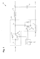
- FIG. 1 shows an exemplary circuit schematic of synchronous buck converter 100 including half-bridge 102, which is formed in a stacked half-bridge package 102, according to an embodiment of the invention, and is thus also referred to as "stack half-bridge package” 102 or "half-bridge package” 102 in the present application.
- Synchronous buck converter 100 also includes, driver integrated circuit (IC) 104, output inductor 106, and output capacitor 108.
- IC driver integrated circuit
- Half-bridge 102 includes control transistor Q 1 and synchronous transistor Q 2 (also referred to as “sync transistor"), high voltage input terminal V H , low voltage input terminal V L , output terminal V OUT , control gate terminal V G1 , and sync gate terminal V G2 .
- high voltage input terminal V H receives high voltage input V HI , which can be, for example, a direct current (DC) voltage.
- Low voltage input terminal V L receives low voltage input V LI , which can be, for example, ground.
- control gate terminal V G1 receives a control gate signal from driver IC 104 for driving control transistor Q 1 .
- sync gate terminal V G2 receives a sync gate signal from driver IC 104 for driving sync transistor Q 2 .
- Driver IC 104 may drive control transistor Q 1 and sync transistor Q 2 utilizing any suitable method.
- driver IC 104 can vary a duty cycle of the sync and control gate signals responsive to a measurement of output voltage V O of synchronous buck converter 100 to maintain a desired output voltage V O , regardless of changes in high voltage input V HI . It will be appreciated that in other embodiments, output voltage V O is not measured in synchronous buck converter 100.
- Control transistor Q 1 includes control source S 1 , control drain D 1 , and control gate G 1 .
- Sync transistor Q 2 includes sync source S 2 , sync drain D 2 , and sync gate G 2 .
- control transistor Q 1 and sync transistor Q 2 can be any combination of an enhancement more transistor and a depletion mode transistor.
- control transistor Q 1 and sync transistor Q 2 are both depletion mode transistors.
- Control transistor Q 1 and sync transistor Q 2 can be P-channel or N-channel transistors.
- control transistor Q 1 and sync transistor Q 2 can be field-effect transistors (FETs).
- at least one of control transistor Q 1 and sync transistor Q 2 is a silicon FET.
- control transistor Q 1 and sync transistor Q 2 may also comprise a non-silicon FET or any other FET in general.
- at least one of control transistor Q 1 and sync transistor Q 2 is a metal-oxide-semiconductor field-effect transistor (MOSFET).
- MOSFET metal-oxide-semiconductor field-effect transistor
- At least one of control transistor Q 1 and sync transistor Q 2 can also be, as an example, a high electron mobility transistor (HEMT), such as a GaN HEMT.
- HEMT high electron mobility transistor
- Control transistor Q 1 has control drain D 1 for connection to high voltage input V HI through high voltage input terminal V H of half-bridge 102. Control transistor Q 1 also has control source S 1 coupled to output terminal V OUT of half-bridge 102. Also, control transistor Q 1 has control gate G 1 coupled to control gate terminal V G1 of half-bridge 102 for being driven by driver IC 104.
- Sync transistor Q 2 has sync drain D 2 for connection to output terminal V OUT of half-bridge 102. Sync transistor Q 2 also has sync source S 2 coupled to low voltage input V LI through low voltage input terminal V L of half-bridge 102. Also, sync transistor Q 2 has sync gate G 2 coupled to sync gate terminal V G2 of half-bridge 102 for being driven by driver IC 104.
- control transistor Q 1 and sync transistor Q 2 can be connected to a diode.
- Figure 1 shows optional diodes 110 and 112.
- diode 110 is coupled to control source S 1 and control drain D 1 , such that diode 110 is in parallel with control transistor Q 1 .
- diode 112 is coupled to sync source S 2 and sync drain D 2 , such that diode 112 is in parallel with control transistor Q 2 .
- at least one of diodes 110 and 112 can be connected with a reverse polarity to that shown in Figure 1 .
- diodes 110 and 112 can be internal to or external to control transistor Q 1 and sync transistor Q 2 .
- control transistor Q 1 and sync transistor Q 2 are MOSFETs and diodes 110 and 112 are respective body diodes of control transistor Q 1 and sync transistor Q 2 .
- Control transistor Q 1 and sync transistor Q 2 are commonly included on respective dies (i.e. a control transistor die and a synchronous transistor die).
- the respective dies may include other components, for example, diode 110 may be on the control transistor die and diode 112 may be on the synchronous transistor die. These other components may also be provided external to the respective dies and can be, for example, on a different die.
- Synchronous buck converter 100 illustrates one power converter, which can benefit from including stacked half-bridge package 102, in accordance with embodiments of the present invention.
- half-bridge 102 is not limited to being included in a synchronous buck converter and can be included in other types of power converters.
- control transistor Q 1 and sync transistor Q 2 can be connected in a stacked half-bridge package, which includes stacked half-bridge package 102, while achieving a small footprint with low parasitic inductance and resistance.
- the stacked half-bridge package can have a small form factor where the stacked half-bridge package does not significantly degrade performance of half bridge 102.
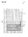
- Figures 2A-2D illustrate selective top views of stacked half-bridge package 202, corresponding to stacked half-bridge package 102 in Figure 1 , in accordance with one embodiment of the present invention.
- Various features of stacked half-bridge package 202 are not shown in Figures 2A-2D for clarity of description.
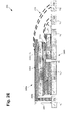
- Figure 2E illustrates a cross sectional view of a portion of stacked half-bridge package 202, according to one embodiment of the invention. The cross sectional view shown in Figure 2E corresponds to a cross section along line 2E-2E in Figures 2A-2D .
- Figure 2A shows control drain leadframe 220, sync source leadframe 222, control gate leadframe 224, sync gate leadframe 226, output terminal leadframe 228, support leadframe 230, and control transistor Q 1 of stacked half-bridge package 202.
- Control transistor Q 1 in Figures 2A-2E corresponds to control transistor Q 1 in Figure 1 .
- Control transistor Q 1 is over control drain leadframe 220 and includes control source S 1 , control drain D 1 , and control gate G 1 .
- Control source S 1 in stacked half-bridge package 202 corresponds to control source S 1 in Figure 1
- control gate G 1 in stacked half bridge package 202 corresponds to control gate G 1 in Figure 1
- control drain D 1 in stacked half-bridge package 202 corresponds to control drain D 1 in Figure 1 .
- control transistor Q 1 has top and bottom surfaces, which are opposite one another. Control drain D 1 is on the bottom surface and control source S 1 and control gate G 1 are on the top surface.
- Figure 2A shows control source S 1 and control gate G 1 are on the top surface of control transistor Q 1 , and indicates control drain D 1 on the bottom surface thereof.
- control drain D 1 is provided with a control drain pad that substantially covers an entirety of the bottom surface of control transistor Q 1 .
- Control source S 1 is provided with a plurality of control source pads 234a and 234b (also referred to collectively as "control source pads 234").
- control gate G 1 is provided with a gate pad.
- control drain D 1 , control source S 1 , and control gate G 1 are not provided as shown in stacked half-bridge package 202.
- control drain D 1 , control source S 1 , and control gate G 1 can be provided on different surfaces of control transistor Q 1 and can be provided using one or more pads arranged in any suitable manner.
- a single control source pad can replace control source pads 234.
- Control drain leadframe 220, sync source leadframe 222, control gate leadframe 224, sync gate leadframe 226, output terminal leadframe 228, and support leadframe 230 are electrically conductive and can comprise, for example, an easily solderable metal such as aluminum, and other solderable materials such as a metal alloy or a tri-metal.
- Control transistor Q 1 is over control drain leadframe 220, which provides mechanical and electrical connection for control drain D 1 .
- control drain leadframe 220 of stacked half-bridge package 202 corresponds to high voltage input terminal V H in Figure 1 .
- At least one control gate bondwire such as control gate bondwires 218, provides electrical and mechanical connection for control gate G 1 .
- Control gate bondwires 218 provide electrical connection between control gate G 1 and control gate leadframe 224.
- control gate leadframe 224 of stacked half-bridge package 202 corresponds to control gate terminal V G1 in Figure 1 . It is noted that some embodiments do not include control gate leadframe 224.
- something other than at least one control gate bondwire e.g. a conductive gate clip
- FIG. 2B is similar to Figure 2A , with an addition of showing common conductive clip 232 of stacked half-bridge package 202 over control drain leadframe 220 and control transistor Q 1 .
- Common conductive clip 232 comprises conductive material, such as a metal or metal alloy. In one embodiment common conductive clip 232 is a copper clip. Control source S 2 of control transistor Q 1 is coupled to common conductive clip 232.
- Common conductive clip 232 includes conductive web 232a and conductive leg 232b.
- a dashed line indicates a boundary of conductive web 232a and conductive leg 232b.
- conductive web 232a is over and electrically and mechanically connected to control source S 2 of control transistor Q 1 and conductive leg 232b is over and electrically and mechanically connected to output terminal leadframe 228.
- Figure 2C is similar to Figure 2B , with an addition of showing sync transistor Q 2 of stacked half-bridge package 202 over common conductive clip 232, control drain leadframe 220, and control transistor Q 1 .
- sync transistor Q 2 is on support leadframe 230, which acts as a mechanical support for sync transistor Q 2 .
- support leadframe 230 is not electrically conductive.
- support leadframe 230 is not required in stacked half-bridge package 202.
- Sync transistor Q 2 in stacked half-bridge package 202 corresponds to sync transistor Q 2 in Figure 1 .
- Sync source S 2 in stacked half-bridge package 202 corresponds to sync source S 2 in Figure 1
- sync gate G 2 in stacked half-bridge package 202 corresponds to sync gate G 2 in Figure 1
- sync drain D 2 in stacked half-bridge package 202 corresponds to sync drain D 2 in Figure 1 .
- sync transistor Q 2 has top and bottom surfaces, which are opposite one another.
- Sync drain D 2 is on the bottom surface and sync source S 2 and sync gate G 2 are on the top surface.
- FIG. 2C shows sync source S 2 and sync gate G 2 are on the top surface of sync transistor Q 2 , and indicates sync drain D 2 on the bottom surface thereof.
- sync drain D 2 is provided with a sync drain pad that substantially covers an entirety of the bottom surface of sync transistor Q 2 .
- Sync source S 2 is provided with a plurality of control source pads 236a, 236b, 236c, 236d, and 236e (also referred to collectively as "sync source pads 236").
- sync gate G 2 is provided with a gate pad.
- sync drain D 2 , sync source S 2 , and sync gate G 2 are not provided as shown in stacked half-bridge package 202.
- sync drain D 2 , sync source S 2 , and sync gate G 2 can be provided on different surfaces of sync transistor Q 2 and can be provided using one or more pads arranged in any suitable manner.
- a single sync source pad can replace sync source pads 236.
- Sync transistor Q 2 is over common conductive clip 232, which is electrically and mechanically connected to sync transistor Q 2 . More particularly, sync transistor Q 2 has sync drain D 2 connected to common conductive clip 232. Conductive web 232a of common conductive clip 232 provides electrical and mechanical coupling of control source S 1 with sync drain D 2 .
- control and sync transistors Q 1 and Q 2 are stacked on opposite sides of common conductive clip 232, with common conductive clip 232 electrically and mechanically coupling control source S 1 with sync drain D 2 .
- a short current path is formed between control source S 1 and sync drain D 2 that has low parasitic inductance and resistance (See Figure 2D ).
- stacked half-bridge package 202 does not significantly degrade performance of half-bridge 102 in Figure 1 .
- stacked half-bridge package 202 has a small footprint that does not incorporate footprints of control transistor Q 1 and sync transistor Q 2 individually, thereby allowing for a small form factor.
- output terminal leadframe 228 corresponds to output terminal V OUT in Figure 1 .
- output terminal leadframe 228 is an output terminal of stacked half-bridge package 202.
- At least one sync gate bondwire such as sync gate bondwires 238, provides electrical and mechanical connection for sync gate G 2 .
- Sync gate bondwires 238 provide electrical connection between sync gate G 2 and sync gate leadframe 226.
- sync gate leadframe 226 of stacked half bridge package 202 corresponds to sync gate terminal V G2 in Figure 1 . It is noted that some embodiments do not include sync gate leadframe 226.
- something other than at least one sync gate bondwire e.g. a conductive gate clip
- Figure 2D is similar to Figure 2C , with an addition of showing conductive source clip 240 of stacked half-bridge package 202 over sync transistor Q 2 , common conductive clip 232, control transistor Q 1 , and control drain leadframe 220.
- Conductive source clip 240 comprises conductive material, such as a metal or metal alloy. In one embodiment conductive source clip 240 is a copper clip.
- Conductive source clip 240 includes source clip web 240a and source clip leg 240b and provides connection between sync source S 2 and sync source leadframe 222.
- a dashed line indicates a boundary of source clip web 240a and source clip leg 240b.
- sync source leadframe 222 corresponds to low voltage input terminal V L in Figure 1
- source clip leadframe 222 corresponds to low voltage input terminal V L in Figure 1
- source clip leg portion 240b being over and electrically and mechanically connected to sync source leadframe 222
- source clip web 240a being over and electrically and mechanically connected to sync source S 2 of sync transistor Q 2 .
- Figure 2E illustrates a cross sectional view of a portion of stacked half-bridge package 202 corresponding to a cross section along line 2E-2E in Figures 2A-2D .
- some features which are not in the cross section along line 2E-2E in Figures 2A-2D are included in Figure 2E for completeness and are indicated using dashed lines.
- Those features are control gate bondwires 218, control gate leadframe 224, sync gate bondwires 238, and sync gate leadframe 226.
- Sync gate bondwires 238 are electrically connected to gate G 2 of sync transistor Q 2 , which is behind and not shown in Figure 2E .
- Figure 2E shows that conductive source clip 240 is connected to sync source S 2 at topside 246a of stacked half-bridge package 202 and shows control drain leadframe 220, sync source leadframe 222, control gate leadframe 224, sync gate leadframe 226, and output terminal leadframe 228 at bottomside 246b of stacked half-bridge package 202.
- hermetic sealant such as a molding compound, can encapsulate stacked half-bridge package 202 (not shown in Figure 2E ).
- control drain leadframe 220, sync source leadframe 222, control gate leadframe 224, sync gate leadframe 226, and output terminal leadframe 228 are exposed on bottomside 246b of stacked half bridge package 202 and thus, available for electrical connection.
- Figure 2E shows conductive leg 232b of common conductive clip 232 is of thickness 242 that is greater than that of control transistor Q 1 and that of conductive web 232b.
- Figure 2E also shows source clip leg 240b of conductive source clip 240 is of thickness 244 that is greater than that of control transistor Q 1 , sync transistor Q 2 , and conductive web 232a combined.
- respective top and bottom surfaces of control drain leadframe 220, sync source leadframe 222, control gate leadframe 224, sync gate leadframe 226, and output terminal leadframe 228 can thereby be substantially flush with one another, as shown in Figure 2E .
- control drain leadframe 220, sync source leadframe 222, control gate leadframe 224, sync gate leadframe 226, and output terminal leadframe 228 can be of substantially a same thickness and in one embodiment, are formed from a shared leadframe.
- embodiments of the present invention can provide for a stacked half-bridge package including a control transistor and a sync transistor.
- the control transistor and the sync transistor can advantageously be connected in a half-bridge with low parasitic inductance and resistance.
- the control transistor and the sync transistor can be connected with the stacked half-bridge package having a small footprint.
- the stacked half-bridge package can have a small form factor, where the stacked half-bridge package does not significantly degrade performance of the half-bridge.
Landscapes
- Dc-Dc Converters (AREA)
- Electronic Switches (AREA)
Applications Claiming Priority (2)
| Application Number | Priority Date | Filing Date | Title |
|---|---|---|---|
| US201161461110P | 2011-01-14 | 2011-01-14 | |
| US13/279,052 US8680627B2 (en) | 2011-01-14 | 2011-10-21 | Stacked half-bridge package with a common conductive clip |
Publications (3)
| Publication Number | Publication Date |
|---|---|
| EP2477220A2 true EP2477220A2 (de) | 2012-07-18 |
| EP2477220A3 EP2477220A3 (de) | 2014-09-24 |
| EP2477220B1 EP2477220B1 (de) | 2019-06-12 |
Family
ID=45047675
Family Applications (1)
| Application Number | Title | Priority Date | Filing Date |
|---|---|---|---|
| EP11191633.4A Not-in-force EP2477220B1 (de) | 2011-01-14 | 2011-12-01 | Gestapelte Halbbrückenverpackung mit gängigem leitfähigem Clip |
Country Status (2)
| Country | Link |
|---|---|
| US (3) | US8680627B2 (de) |
| EP (1) | EP2477220B1 (de) |
Cited By (5)
| Publication number | Priority date | Publication date | Assignee | Title |
|---|---|---|---|---|
| US20140159217A1 (en) * | 2012-12-06 | 2014-06-12 | Magnachip Semiconductor, Ltd. | Multichip package and fabrication method thereof |
| WO2015073980A1 (en) * | 2013-11-15 | 2015-05-21 | Texas Instruments Incorporated | Method and circuitry for controlling a depletion-mode transistor |
| WO2016209934A1 (en) * | 2015-06-23 | 2016-12-29 | Texas Instruments Incorporation | High voltage device with multi-electrode control |
| CN112768424A (zh) * | 2021-01-21 | 2021-05-07 | 厦门市必易微电子技术有限公司 | 一种采用功率半桥叠封方案的半导体器件和半桥电路模块 |
| DE102017109515B4 (de) | 2017-05-04 | 2024-10-02 | Schaeffler Technologies AG & Co. KG | Halbleiteranordnung und Verfahren zu deren Herstellung |
Families Citing this family (21)
| Publication number | Priority date | Publication date | Assignee | Title |
|---|---|---|---|---|
| US8497574B2 (en) * | 2011-01-03 | 2013-07-30 | International Rectifier Corporation | High power semiconductor package with conductive clips and flip chip driver IC |
| US20120200281A1 (en) * | 2011-02-07 | 2012-08-09 | Texas Instruments Incorporated | Three-Dimensional Power Supply Module Having Reduced Switch Node Ringing |
| US8344464B2 (en) * | 2011-05-19 | 2013-01-01 | International Rectifier Corporation | Multi-transistor exposed conductive clip for high power semiconductor packages |
| US9111921B2 (en) * | 2012-10-18 | 2015-08-18 | International Rectifier Corporation | Semiconductor package with conductive carrier integrated heat spreader |
| US9111776B2 (en) | 2012-10-18 | 2015-08-18 | International Rectifier Corporation | Power semiconductor package with non-contiguous, multi-section conductive carrier |
| US8860194B2 (en) * | 2012-11-01 | 2014-10-14 | International Rectifier Corporation | Buck converter power package |
| US9171837B2 (en) * | 2012-12-17 | 2015-10-27 | Nxp B.V. | Cascode circuit |
| US9214415B2 (en) * | 2013-04-11 | 2015-12-15 | Texas Instruments Incorporated | Integrating multi-output power converters having vertically stacked semiconductor chips |
| US10242969B2 (en) * | 2013-11-12 | 2019-03-26 | Infineon Technologies Ag | Semiconductor package comprising a transistor chip module and a driver chip module and a method for fabricating the same |
| US9196510B2 (en) | 2013-11-12 | 2015-11-24 | Infineon Technologies Ag | Semiconductor package comprising two semiconductor modules and laterally extending connectors |
| US9536800B2 (en) | 2013-12-07 | 2017-01-03 | Fairchild Semiconductor Corporation | Packaged semiconductor devices and methods of manufacturing |
| US9564389B2 (en) * | 2014-03-18 | 2017-02-07 | Infineon Technologies Americas Corp. | Semiconductor package with integrated die paddles for power stage |
| US20160104688A1 (en) * | 2014-10-09 | 2016-04-14 | International Rectifier Corporation | Robust and Reliable Power Semiconductor Package |
| US20160172279A1 (en) * | 2014-12-10 | 2016-06-16 | Infineon Technologies Americas Corp. | Integrated Power Assembly with Reduced Form Factor and Enhanced Thermal Dissipation |
| US9768099B1 (en) | 2016-05-06 | 2017-09-19 | Infineon Technologies Americas Corp. | IC package with integrated inductor |
| US10332825B2 (en) * | 2016-05-20 | 2019-06-25 | Infineon Technologies Americas Corp. | Semiconductor package including flip chip mounted IC and vertically integrated inductor |
| US10128170B2 (en) | 2017-01-09 | 2018-11-13 | Silanna Asia Pte Ltd | Conductive clip connection arrangements for semiconductor packages |
| US11075154B2 (en) * | 2017-10-26 | 2021-07-27 | Shindengen Electric Manufacturing Co., Ltd. | Semiconductor device and method of manufacturing semiconductor device |
| WO2019197304A1 (en) * | 2018-04-11 | 2019-10-17 | Abb Schweiz Ag | Material reduced metallic plate on power semiconductor chip |
| CN110660768B (zh) * | 2018-06-28 | 2021-02-26 | 朋程科技股份有限公司 | 用于整流器的功率器件 |
| CN118099152A (zh) * | 2022-11-25 | 2024-05-28 | 无锡华润华晶微电子有限公司 | 一种GaN器件封装结构及其封装方法 |
Citations (1)
| Publication number | Priority date | Publication date | Assignee | Title |
|---|---|---|---|---|
| US7902809B2 (en) | 2006-11-28 | 2011-03-08 | International Rectifier Corporation | DC/DC converter including a depletion mode power switch |
Family Cites Families (25)
| Publication number | Priority date | Publication date | Assignee | Title |
|---|---|---|---|---|
| US5043859A (en) * | 1989-12-21 | 1991-08-27 | General Electric Company | Half bridge device package, packaged devices and circuits |
| US7227198B2 (en) * | 2004-08-11 | 2007-06-05 | International Rectifier Corporation | Half-bridge package |
| JP4426955B2 (ja) | 2004-11-30 | 2010-03-03 | 株式会社ルネサステクノロジ | 半導体装置 |
| JP2006216940A (ja) | 2005-01-07 | 2006-08-17 | Toshiba Corp | 半導体装置 |
| JP2006324320A (ja) | 2005-05-17 | 2006-11-30 | Renesas Technology Corp | 半導体装置 |
| DE102005055761B4 (de) | 2005-11-21 | 2008-02-07 | Infineon Technologies Ag | Leistungshalbleiterbauelement mit Halbleiterchipstapel in Brückenschaltung und Verfahren zur Herstellung desselben |
| US7618896B2 (en) | 2006-04-24 | 2009-11-17 | Fairchild Semiconductor Corporation | Semiconductor die package including multiple dies and a common node structure |
| US7859089B2 (en) | 2006-05-04 | 2010-12-28 | International Rectifier Corporation | Copper straps |
| US7485954B2 (en) * | 2006-09-07 | 2009-02-03 | Alpha And Omega Semiconductor Limited | Stacked dual MOSFET package |
| US8674670B2 (en) | 2006-11-28 | 2014-03-18 | International Rectifier Corporation | DC/DC converter with depletion-mode III-nitride switches |
| KR101489325B1 (ko) | 2007-03-12 | 2015-02-06 | 페어차일드코리아반도체 주식회사 | 플립-칩 방식의 적층형 파워 모듈 및 그 파워 모듈의제조방법 |
| US7800208B2 (en) * | 2007-10-26 | 2010-09-21 | Infineon Technologies Ag | Device with a plurality of semiconductor chips |
| KR101375831B1 (ko) * | 2007-12-03 | 2014-04-02 | 삼성전자주식회사 | 산화물 반도체 박막 트랜지스터를 이용한 디스플레이 장치 |
| KR20090062612A (ko) | 2007-12-13 | 2009-06-17 | 페어차일드코리아반도체 주식회사 | 멀티 칩 패키지 |
| US7781872B2 (en) | 2007-12-19 | 2010-08-24 | Fairchild Semiconductor Corporation | Package with multiple dies |
| US8642394B2 (en) | 2008-01-28 | 2014-02-04 | Infineon Technologies Ag | Method of manufacturing electronic device on leadframe |
| KR100958006B1 (ko) * | 2008-06-18 | 2010-05-17 | 삼성모바일디스플레이주식회사 | 박막 트랜지스터, 그의 제조 방법 및 박막 트랜지스터를구비하는 평판 표시 장치 |
| US8062932B2 (en) | 2008-12-01 | 2011-11-22 | Alpha & Omega Semiconductor, Inc. | Compact semiconductor package with integrated bypass capacitor and method |
| US20100171543A1 (en) | 2009-01-08 | 2010-07-08 | Ciclon Semiconductor Device Corp. | Packaged power switching device |
| KR101097322B1 (ko) * | 2009-12-15 | 2011-12-23 | 삼성모바일디스플레이주식회사 | 산화물 반도체 박막 트랜지스터, 그 제조방법 및 산화물 반도체 박막 트랜지스터를 구비한 유기전계 발광소자 |
| US8497574B2 (en) | 2011-01-03 | 2013-07-30 | International Rectifier Corporation | High power semiconductor package with conductive clips and flip chip driver IC |
| US8426952B2 (en) * | 2011-01-14 | 2013-04-23 | International Rectifier Corporation | Stacked half-bridge package with a common conductive leadframe |
| DE102011008952A1 (de) | 2011-01-19 | 2012-07-19 | Texas Instruments Deutschland Gmbh | Mehrchipmodul, Verfahren zum Betreiben desselben und DC/DC-Wandler |
| US8299588B1 (en) | 2011-07-07 | 2012-10-30 | Texas Instruments Incorporated | Structure and method for uniform current distribution in power supply module |
| US8860194B2 (en) | 2012-11-01 | 2014-10-14 | International Rectifier Corporation | Buck converter power package |
-
2011
- 2011-10-21 US US13/279,052 patent/US8680627B2/en not_active Expired - Fee Related
- 2011-12-01 EP EP11191633.4A patent/EP2477220B1/de not_active Not-in-force
-
2014
- 2014-03-21 US US14/221,518 patent/US9048230B2/en active Active
-
2015
- 2015-05-27 US US14/722,974 patent/US9461022B2/en active Active
Patent Citations (1)
| Publication number | Priority date | Publication date | Assignee | Title |
|---|---|---|---|---|
| US7902809B2 (en) | 2006-11-28 | 2011-03-08 | International Rectifier Corporation | DC/DC converter including a depletion mode power switch |
Cited By (11)
| Publication number | Priority date | Publication date | Assignee | Title |
|---|---|---|---|---|
| US20140159217A1 (en) * | 2012-12-06 | 2014-06-12 | Magnachip Semiconductor, Ltd. | Multichip package and fabrication method thereof |
| US11362022B2 (en) * | 2012-12-06 | 2022-06-14 | Magnachip Semiconductor, Ltd. | Multichip package semiconductor device |
| US12057377B2 (en) | 2012-12-06 | 2024-08-06 | Magnachip Semiconductor, Ltd. | Multichip packaged semiconductor device |
| WO2015073980A1 (en) * | 2013-11-15 | 2015-05-21 | Texas Instruments Incorporated | Method and circuitry for controlling a depletion-mode transistor |
| US9762230B2 (en) | 2013-11-15 | 2017-09-12 | Texas Instruments Incorporated | Method and circuitry for controlling a depletion-mode transistor |
| US11356087B2 (en) | 2013-11-15 | 2022-06-07 | Texas Instruments Incorporated | Method and circuitry for controlling a depletion-mode transistor |
| WO2016209934A1 (en) * | 2015-06-23 | 2016-12-29 | Texas Instruments Incorporation | High voltage device with multi-electrode control |
| US9991225B2 (en) | 2015-06-23 | 2018-06-05 | Texas Instruments Incorporated | High voltage device with multi-electrode control |
| US10340252B2 (en) | 2015-06-23 | 2019-07-02 | Texas Instruments Incorporated | High voltage device with multi-electrode control |
| DE102017109515B4 (de) | 2017-05-04 | 2024-10-02 | Schaeffler Technologies AG & Co. KG | Halbleiteranordnung und Verfahren zu deren Herstellung |
| CN112768424A (zh) * | 2021-01-21 | 2021-05-07 | 厦门市必易微电子技术有限公司 | 一种采用功率半桥叠封方案的半导体器件和半桥电路模块 |
Also Published As
| Publication number | Publication date |
|---|---|
| EP2477220A3 (de) | 2014-09-24 |
| US9048230B2 (en) | 2015-06-02 |
| US20150279821A1 (en) | 2015-10-01 |
| EP2477220B1 (de) | 2019-06-12 |
| US8680627B2 (en) | 2014-03-25 |
| US20140203419A1 (en) | 2014-07-24 |
| US9461022B2 (en) | 2016-10-04 |
| US20120181624A1 (en) | 2012-07-19 |
Similar Documents
| Publication | Publication Date | Title |
|---|---|---|
| EP2477220B1 (de) | Gestapelte Halbbrückenverpackung mit gängigem leitfähigem Clip | |
| US9583477B2 (en) | Stacked half-bridge package | |
| EP2477222B1 (de) | Gestapelte Halbbrückenverpackung mit einer stromführenden Schicht | |
| US8497574B2 (en) | High power semiconductor package with conductive clips and flip chip driver IC | |
| US9653386B2 (en) | Compact multi-die power semiconductor package | |
| US10438876B2 (en) | Power quad flat no-lead (PQFN) package in a single shunt inverter circuit | |
| US20100090668A1 (en) | Stacked Field Effect Transistor Configurations | |
| US20070108575A1 (en) | Semiconductor package that includes stacked semiconductor die | |
| US9831159B2 (en) | Semiconductor package with embedded output inductor | |
| US11990455B2 (en) | Semiconductor device | |
| US8901742B2 (en) | Monolithic Power Converter Package with Through Substrate vias | |
| US9041175B2 (en) | Monolithic power converter package | |
| JP6235918B2 (ja) | シングルシャントインバータ回路に含まれるパワー・カッド・フラット・ノーリード(pqfn)パッケージ | |
| TWI570878B (zh) | 在共同積體電路上具有自舉二極體的功率四面扁平無引線封裝 |
Legal Events
| Date | Code | Title | Description |
|---|---|---|---|
| PUAI | Public reference made under article 153(3) epc to a published international application that has entered the european phase |
Free format text: ORIGINAL CODE: 0009012 |
|
| AK | Designated contracting states |
Kind code of ref document: A2 Designated state(s): AL AT BE BG CH CY CZ DE DK EE ES FI FR GB GR HR HU IE IS IT LI LT LU LV MC MK MT NL NO PL PT RO RS SE SI SK SM TR |
|
| AX | Request for extension of the european patent |
Extension state: BA ME |
|
| PUAL | Search report despatched |
Free format text: ORIGINAL CODE: 0009013 |
|
| AK | Designated contracting states |
Kind code of ref document: A3 Designated state(s): AL AT BE BG CH CY CZ DE DK EE ES FI FR GB GR HR HU IE IS IT LI LT LU LV MC MK MT NL NO PL PT RO RS SE SI SK SM TR |
|
| AX | Request for extension of the european patent |
Extension state: BA ME |
|
| RIC1 | Information provided on ipc code assigned before grant |
Ipc: H01L 23/495 20060101AFI20140815BHEP |
|
| 17P | Request for examination filed |
Effective date: 20150324 |
|
| RBV | Designated contracting states (corrected) |
Designated state(s): AL AT BE BG CH CY CZ DE DK EE ES FI FR GB GR HR HU IE IS IT LI LT LU LV MC MK MT NL NO PL PT RO RS SE SI SK SM TR |
|
| STAA | Information on the status of an ep patent application or granted ep patent |
Free format text: STATUS: EXAMINATION IS IN PROGRESS |
|
| 17Q | First examination report despatched |
Effective date: 20171128 |
|
| RAP1 | Party data changed (applicant data changed or rights of an application transferred) |
Owner name: INFINEON TECHNOLOGIES AMERICAS CORP. |
|
| GRAP | Despatch of communication of intention to grant a patent |
Free format text: ORIGINAL CODE: EPIDOSNIGR1 |
|
| STAA | Information on the status of an ep patent application or granted ep patent |
Free format text: STATUS: GRANT OF PATENT IS INTENDED |
|
| INTG | Intention to grant announced |
Effective date: 20181218 |
|
| GRAS | Grant fee paid |
Free format text: ORIGINAL CODE: EPIDOSNIGR3 |
|
| GRAA | (expected) grant |
Free format text: ORIGINAL CODE: 0009210 |
|
| STAA | Information on the status of an ep patent application or granted ep patent |
Free format text: STATUS: THE PATENT HAS BEEN GRANTED |
|
| AK | Designated contracting states |
Kind code of ref document: B1 Designated state(s): AL AT BE BG CH CY CZ DE DK EE ES FI FR GB GR HR HU IE IS IT LI LT LU LV MC MK MT NL NO PL PT RO RS SE SI SK SM TR |
|
| REG | Reference to a national code |
Ref country code: GB Ref legal event code: FG4D |
|
| REG | Reference to a national code |
Ref country code: CH Ref legal event code: EP |
|
| REG | Reference to a national code |
Ref country code: AT Ref legal event code: REF Ref document number: 1143690 Country of ref document: AT Kind code of ref document: T Effective date: 20190615 |
|
| REG | Reference to a national code |
Ref country code: DE Ref legal event code: R096 Ref document number: 602011059585 Country of ref document: DE |
|
| REG | Reference to a national code |
Ref country code: IE Ref legal event code: FG4D |
|
| REG | Reference to a national code |
Ref country code: NL Ref legal event code: MP Effective date: 20190612 |
|
| REG | Reference to a national code |
Ref country code: LT Ref legal event code: MG4D |
|
| PG25 | Lapsed in a contracting state [announced via postgrant information from national office to epo] |
Ref country code: NO Free format text: LAPSE BECAUSE OF FAILURE TO SUBMIT A TRANSLATION OF THE DESCRIPTION OR TO PAY THE FEE WITHIN THE PRESCRIBED TIME-LIMIT Effective date: 20190912 Ref country code: LT Free format text: LAPSE BECAUSE OF FAILURE TO SUBMIT A TRANSLATION OF THE DESCRIPTION OR TO PAY THE FEE WITHIN THE PRESCRIBED TIME-LIMIT Effective date: 20190612 Ref country code: FI Free format text: LAPSE BECAUSE OF FAILURE TO SUBMIT A TRANSLATION OF THE DESCRIPTION OR TO PAY THE FEE WITHIN THE PRESCRIBED TIME-LIMIT Effective date: 20190612 Ref country code: ES Free format text: LAPSE BECAUSE OF FAILURE TO SUBMIT A TRANSLATION OF THE DESCRIPTION OR TO PAY THE FEE WITHIN THE PRESCRIBED TIME-LIMIT Effective date: 20190612 Ref country code: AL Free format text: LAPSE BECAUSE OF FAILURE TO SUBMIT A TRANSLATION OF THE DESCRIPTION OR TO PAY THE FEE WITHIN THE PRESCRIBED TIME-LIMIT Effective date: 20190612 Ref country code: HR Free format text: LAPSE BECAUSE OF FAILURE TO SUBMIT A TRANSLATION OF THE DESCRIPTION OR TO PAY THE FEE WITHIN THE PRESCRIBED TIME-LIMIT Effective date: 20190612 Ref country code: SE Free format text: LAPSE BECAUSE OF FAILURE TO SUBMIT A TRANSLATION OF THE DESCRIPTION OR TO PAY THE FEE WITHIN THE PRESCRIBED TIME-LIMIT Effective date: 20190612 |
|
| PG25 | Lapsed in a contracting state [announced via postgrant information from national office to epo] |
Ref country code: LV Free format text: LAPSE BECAUSE OF FAILURE TO SUBMIT A TRANSLATION OF THE DESCRIPTION OR TO PAY THE FEE WITHIN THE PRESCRIBED TIME-LIMIT Effective date: 20190612 Ref country code: GR Free format text: LAPSE BECAUSE OF FAILURE TO SUBMIT A TRANSLATION OF THE DESCRIPTION OR TO PAY THE FEE WITHIN THE PRESCRIBED TIME-LIMIT Effective date: 20190913 Ref country code: BG Free format text: LAPSE BECAUSE OF FAILURE TO SUBMIT A TRANSLATION OF THE DESCRIPTION OR TO PAY THE FEE WITHIN THE PRESCRIBED TIME-LIMIT Effective date: 20190912 Ref country code: RS Free format text: LAPSE BECAUSE OF FAILURE TO SUBMIT A TRANSLATION OF THE DESCRIPTION OR TO PAY THE FEE WITHIN THE PRESCRIBED TIME-LIMIT Effective date: 20190612 |
|
| REG | Reference to a national code |
Ref country code: AT Ref legal event code: MK05 Ref document number: 1143690 Country of ref document: AT Kind code of ref document: T Effective date: 20190612 |
|
| PG25 | Lapsed in a contracting state [announced via postgrant information from national office to epo] |
Ref country code: SK Free format text: LAPSE BECAUSE OF FAILURE TO SUBMIT A TRANSLATION OF THE DESCRIPTION OR TO PAY THE FEE WITHIN THE PRESCRIBED TIME-LIMIT Effective date: 20190612 Ref country code: EE Free format text: LAPSE BECAUSE OF FAILURE TO SUBMIT A TRANSLATION OF THE DESCRIPTION OR TO PAY THE FEE WITHIN THE PRESCRIBED TIME-LIMIT Effective date: 20190612 Ref country code: CZ Free format text: LAPSE BECAUSE OF FAILURE TO SUBMIT A TRANSLATION OF THE DESCRIPTION OR TO PAY THE FEE WITHIN THE PRESCRIBED TIME-LIMIT Effective date: 20190612 Ref country code: RO Free format text: LAPSE BECAUSE OF FAILURE TO SUBMIT A TRANSLATION OF THE DESCRIPTION OR TO PAY THE FEE WITHIN THE PRESCRIBED TIME-LIMIT Effective date: 20190612 Ref country code: NL Free format text: LAPSE BECAUSE OF FAILURE TO SUBMIT A TRANSLATION OF THE DESCRIPTION OR TO PAY THE FEE WITHIN THE PRESCRIBED TIME-LIMIT Effective date: 20190612 Ref country code: AT Free format text: LAPSE BECAUSE OF FAILURE TO SUBMIT A TRANSLATION OF THE DESCRIPTION OR TO PAY THE FEE WITHIN THE PRESCRIBED TIME-LIMIT Effective date: 20190612 Ref country code: PT Free format text: LAPSE BECAUSE OF FAILURE TO SUBMIT A TRANSLATION OF THE DESCRIPTION OR TO PAY THE FEE WITHIN THE PRESCRIBED TIME-LIMIT Effective date: 20191014 |
|
| PG25 | Lapsed in a contracting state [announced via postgrant information from national office to epo] |
Ref country code: IT Free format text: LAPSE BECAUSE OF FAILURE TO SUBMIT A TRANSLATION OF THE DESCRIPTION OR TO PAY THE FEE WITHIN THE PRESCRIBED TIME-LIMIT Effective date: 20190612 Ref country code: IS Free format text: LAPSE BECAUSE OF FAILURE TO SUBMIT A TRANSLATION OF THE DESCRIPTION OR TO PAY THE FEE WITHIN THE PRESCRIBED TIME-LIMIT Effective date: 20191012 Ref country code: SM Free format text: LAPSE BECAUSE OF FAILURE TO SUBMIT A TRANSLATION OF THE DESCRIPTION OR TO PAY THE FEE WITHIN THE PRESCRIBED TIME-LIMIT Effective date: 20190612 |
|
| REG | Reference to a national code |
Ref country code: DE Ref legal event code: R097 Ref document number: 602011059585 Country of ref document: DE |
|
| PG25 | Lapsed in a contracting state [announced via postgrant information from national office to epo] |
Ref country code: TR Free format text: LAPSE BECAUSE OF FAILURE TO SUBMIT A TRANSLATION OF THE DESCRIPTION OR TO PAY THE FEE WITHIN THE PRESCRIBED TIME-LIMIT Effective date: 20190612 |
|
| PLBE | No opposition filed within time limit |
Free format text: ORIGINAL CODE: 0009261 |
|
| STAA | Information on the status of an ep patent application or granted ep patent |
Free format text: STATUS: NO OPPOSITION FILED WITHIN TIME LIMIT |
|
| PG25 | Lapsed in a contracting state [announced via postgrant information from national office to epo] |
Ref country code: DK Free format text: LAPSE BECAUSE OF FAILURE TO SUBMIT A TRANSLATION OF THE DESCRIPTION OR TO PAY THE FEE WITHIN THE PRESCRIBED TIME-LIMIT Effective date: 20190612 Ref country code: PL Free format text: LAPSE BECAUSE OF FAILURE TO SUBMIT A TRANSLATION OF THE DESCRIPTION OR TO PAY THE FEE WITHIN THE PRESCRIBED TIME-LIMIT Effective date: 20190612 |
|
| 26N | No opposition filed |
Effective date: 20200313 |
|
| PG25 | Lapsed in a contracting state [announced via postgrant information from national office to epo] |
Ref country code: SI Free format text: LAPSE BECAUSE OF FAILURE TO SUBMIT A TRANSLATION OF THE DESCRIPTION OR TO PAY THE FEE WITHIN THE PRESCRIBED TIME-LIMIT Effective date: 20190612 Ref country code: IS Free format text: LAPSE BECAUSE OF FAILURE TO SUBMIT A TRANSLATION OF THE DESCRIPTION OR TO PAY THE FEE WITHIN THE PRESCRIBED TIME-LIMIT Effective date: 20200224 |
|
| PG2D | Information on lapse in contracting state deleted |
Ref country code: IS |
|
| REG | Reference to a national code |
Ref country code: CH Ref legal event code: PL |
|
| REG | Reference to a national code |
Ref country code: BE Ref legal event code: MM Effective date: 20191231 |
|
| PG25 | Lapsed in a contracting state [announced via postgrant information from national office to epo] |
Ref country code: MC Free format text: LAPSE BECAUSE OF FAILURE TO SUBMIT A TRANSLATION OF THE DESCRIPTION OR TO PAY THE FEE WITHIN THE PRESCRIBED TIME-LIMIT Effective date: 20190612 |
|
| GBPC | Gb: european patent ceased through non-payment of renewal fee |
Effective date: 20191201 |
|
| PG25 | Lapsed in a contracting state [announced via postgrant information from national office to epo] |
Ref country code: GB Free format text: LAPSE BECAUSE OF NON-PAYMENT OF DUE FEES Effective date: 20191201 Ref country code: FR Free format text: LAPSE BECAUSE OF NON-PAYMENT OF DUE FEES Effective date: 20191231 Ref country code: LU Free format text: LAPSE BECAUSE OF NON-PAYMENT OF DUE FEES Effective date: 20191201 Ref country code: IE Free format text: LAPSE BECAUSE OF NON-PAYMENT OF DUE FEES Effective date: 20191201 |
|
| PG25 | Lapsed in a contracting state [announced via postgrant information from national office to epo] |
Ref country code: CH Free format text: LAPSE BECAUSE OF NON-PAYMENT OF DUE FEES Effective date: 20191231 Ref country code: LI Free format text: LAPSE BECAUSE OF NON-PAYMENT OF DUE FEES Effective date: 20191231 Ref country code: BE Free format text: LAPSE BECAUSE OF NON-PAYMENT OF DUE FEES Effective date: 20191231 |
|
| PG25 | Lapsed in a contracting state [announced via postgrant information from national office to epo] |
Ref country code: CY Free format text: LAPSE BECAUSE OF FAILURE TO SUBMIT A TRANSLATION OF THE DESCRIPTION OR TO PAY THE FEE WITHIN THE PRESCRIBED TIME-LIMIT Effective date: 20190612 |
|
| PG25 | Lapsed in a contracting state [announced via postgrant information from national office to epo] |
Ref country code: HU Free format text: LAPSE BECAUSE OF FAILURE TO SUBMIT A TRANSLATION OF THE DESCRIPTION OR TO PAY THE FEE WITHIN THE PRESCRIBED TIME-LIMIT; INVALID AB INITIO Effective date: 20111201 Ref country code: MT Free format text: LAPSE BECAUSE OF FAILURE TO SUBMIT A TRANSLATION OF THE DESCRIPTION OR TO PAY THE FEE WITHIN THE PRESCRIBED TIME-LIMIT Effective date: 20190612 |
|
| PGFP | Annual fee paid to national office [announced via postgrant information from national office to epo] |
Ref country code: DE Payment date: 20220225 Year of fee payment: 11 |
|
| PG25 | Lapsed in a contracting state [announced via postgrant information from national office to epo] |
Ref country code: MK Free format text: LAPSE BECAUSE OF FAILURE TO SUBMIT A TRANSLATION OF THE DESCRIPTION OR TO PAY THE FEE WITHIN THE PRESCRIBED TIME-LIMIT Effective date: 20190612 |
|
| REG | Reference to a national code |
Ref country code: DE Ref legal event code: R119 Ref document number: 602011059585 Country of ref document: DE |
|
| PG25 | Lapsed in a contracting state [announced via postgrant information from national office to epo] |
Ref country code: DE Free format text: LAPSE BECAUSE OF NON-PAYMENT OF DUE FEES Effective date: 20230701 |