EP2473915B1 - An internal processing-unit memory for general-purpose use - Google Patents
An internal processing-unit memory for general-purpose use Download PDFInfo
- Publication number
- EP2473915B1 EP2473915B1 EP10754627.7A EP10754627A EP2473915B1 EP 2473915 B1 EP2473915 B1 EP 2473915B1 EP 10754627 A EP10754627 A EP 10754627A EP 2473915 B1 EP2473915 B1 EP 2473915B1
- Authority
- EP
- European Patent Office
- Prior art keywords
- memory
- internal memory
- gpu
- processing unit
- access
- Prior art date
- Legal status (The legal status is an assumption and is not a legal conclusion. Google has not performed a legal analysis and makes no representation as to the accuracy of the status listed.)
- Active
Links
Images


Classifications
-
- G—PHYSICS
- G06—COMPUTING OR CALCULATING; COUNTING
- G06F—ELECTRIC DIGITAL DATA PROCESSING
- G06F9/00—Arrangements for program control, e.g. control units
- G06F9/06—Arrangements for program control, e.g. control units using stored programs, i.e. using an internal store of processing equipment to receive or retain programs
- G06F9/30—Arrangements for executing machine instructions, e.g. instruction decode
- G06F9/38—Concurrent instruction execution, e.g. pipeline or look ahead
- G06F9/3877—Concurrent instruction execution, e.g. pipeline or look ahead using a slave processor, e.g. coprocessor
- G06F9/3879—Concurrent instruction execution, e.g. pipeline or look ahead using a slave processor, e.g. coprocessor for non-native instruction execution, e.g. executing a command; for Java instruction set
-
- G—PHYSICS
- G06—COMPUTING OR CALCULATING; COUNTING
- G06F—ELECTRIC DIGITAL DATA PROCESSING
- G06F9/00—Arrangements for program control, e.g. control units
- G06F9/06—Arrangements for program control, e.g. control units using stored programs, i.e. using an internal store of processing equipment to receive or retain programs
- G06F9/46—Multiprogramming arrangements
- G06F9/54—Interprogram communication
- G06F9/544—Buffers; Shared memory; Pipes
Definitions
- the present invention is generally directed to computing devices (e.g., computers, embedded devices, hand-held devices, and the like). More particularly, the present invention is directed to memory used by processing units of such computing devices.
- a computing device typically includes one or more processing units, such as a central-processing unit (CPU) and a graphics-processing unit (GPU).
- the CPU coordinates the activities of the computing device by following a precise set of instructions.
- the GPU assists the CPU by performing data-parallel computing tasks, such as graphics-processing tasks and/or physics simulations which may be required by an end-user application (e.g., a video-game application).
- the GPU and CPU may be part of separate devices and/or packages or may be included in the same device and/or package. Further, each processing unit may be included in another larger device. For example, GPUs are frequently integrated into routing or bridge devices such as, for example, Northbridge devices.
- the end-user application communicates with an application-programming interface (API).
- API allows the end-user application to output graphics data and commands in a standardized format, rather than in a format that is dependent on the GPU.
- Several types of APIs are commercially available - including DirectX® developed by Microsoft Corporation of Redmond, Washington; OpenGL® and OpenCL maintained by Khronos Group.
- the API communicates with a driver.
- the driver translates standard code received from the API into a native format of instructions understood by the GPU.
- the driver is typically written by the manufacturer of the GPU.
- the GPU then executes the instructions from the driver.
- the CPU and GPU are each typically coupled to an external memory.
- the external memory may include instructions to be executed and/or data to be used by the CPU and/or GPU.
- the external memory may be, for example, a dynamic random-access memory (DRAM).
- DRAM dynamic random-access memory
- the external memory can be configured to be quite large, thereby providing ample storage capacity to each processing unit to which it's coupled. Unfortunately, accessing the external memory may take several hundred clock cycles. Accordingly, an external memory may not provide memory sufficient bandwidth or fast memory access for high-end GPUs
- the internal memory may be, for example, an embedded or stacked DRAM.
- an internal memory provides higher bandwidth, faster memory access, and consumes less power.
- the capacity of the internal memory cannot easily be scaled to meet the storage demands of high-end GPUs.
- a high-end GPU may require more memory than can be included in an internal memory of the GPU.
- the invention is the GPU, computer program product and system of claims 1, 12 and 15.
- Embodiments of the present invention meets the above-described needs by providing an internal, processing-unit memory for general-purpose use and applications thereof.
- the internal, processing-unit memory of embodiments of the present invention provides high bandwidth because it is embedded within a processing unit. It also provides sufficient storage capacity because a plurality of processing-unit memories may be combined into a sufficiently large memory pool.
- an embodiment of the present invention provides a GPU.
- the GPU includes a first internal memory, an execution unit coupled to the first internal memory, and an interface configured to couple the first internal memory to a second internal memory of another processing unit.
- the GPU is embodied in software.
- the GPU is included in a system
- the system may comprise, for example, a supercomputer, a desktop computer, a laptop computer, a video-game console, an embedded device, a handheld device (e.g., a mobile telephone, smart phone, MP3 player, a camera, a GPS device, or the like), or another system that includes or is configured to include a GPU.
- the present invention provides an internal, GPU memory for general-purpose use and applications thereof.
- references to "one embodiment,” “an embodiment,” “an example embodiment,” etc. indicate that the embodiment described may include a particular feature, structure, or characteristic, but every embodiment may not necessarily include the particular feature, structure, or characteristic. Moreover, such phrases are not necessarily referring to the same embodiment. Further, when a particular feature, structure, or characteristic is described in connection with an embodiment, it is submitted that it is within the knowledge of one skilled in the art to affect such feature, structure, or characteristic in connection with other embodiments whether or not explicitly described.
- a GPU includes an internal memory (e.g., an embedded or stacked DRAM) that is configured to be used by one or more other processing units.
- the GPU includes an interface and implements a protocol, allowing the one or more other GPUs access to its internal memory.
- the interface may provide each other GPUs dedicated access to the internal memory or may provide the other GPUs shared access to the internal memory. Access to the internal memory of the GPU may be controlled by the GPU itself or each other GPUs.
- the interface and protocol allows the internal memory to be combined with external memories, forming a larger memory pool accessible to the GPU.
- the external memories may be included in other GPUs.
- a computing device includes a plurality of GPUs, wherein each GPU includes an internal memory that is configured to be shared with the other GPUs.
- the internal memory of each GPU is combined into a unified memory pool. The size of the memory pool scales with the number of participating GPUs. Any participating GPU may use the memory pool for its storage needs.
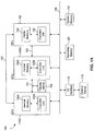
- FIGS. 1A and 1B illustrate an example computing system 100 having a plurality of GPUs, each including an internal memory configured for general-purpose use in accordance with embodiments of the present invention.
- the internal memories provide each GPU higher bandwidth access to data.
- the internal memories of each GPU can be combined into a larger memory pool accessible by each GPU, thereby providing sufficient storage capacity to each GPU.
- each GPU is given dedicated access to the internal memory of another GPU.
- each GPU has shared access to the internal memories of the other GPU via a shared interface.
- computing system 100 may comprise a supercomputer, a desktop computer, a laptop computer, a video-game console, an embedded device, a handheld device (e.g., a mobile telephone, smart phone, MP3 player, a camera, a GPS device, or the like), or some other device that includes or is configured to include a CPU and/or GPU.
- computing device 100 includes a CPU 102, a first GPU 110A, and a second GPU 110B.
- CPU 102 executes instructions to control the functionality of computing device 100.
- GPUs 110 assist CPU 102 by performing data-parallel processing tasks (such as, for example, graphics-processing tasks and/or general-compute tasks). Based on their design, GPUs 110 can typically perform data-parallel processing tasks faster than CPU 102 could perform them in software.
- First GPU 110A and second GPU 110B each include their own internal memory and execution unit.
- first GPU 106A includes an internal memory 106A and an execution unit 142A; and second GPU 106B includes an internal memory 106B and an execution unit 142B.
- CPU 102 includes a cache memory 130 and an execution unit 132.
- Internal memories 106 (and optionally cache memory 130) are available to GPUs 110 to provide faster access and higher bandwidth to certain data than would be possible if the data were externally stored (e.g., if the data were stored in a system memory 104).
- the internal memories 106 may comprise, for example, embedded or stacked DRAM
- Internal memories 106A, 106B may be combined into a larger memory pool to provide substantial storage capacity (e.g., more than 4 GB), while also providing fast, high bandwidth memory access.
- conventional external memories may provide sufficient storage capacity (e.g., more than 4 GB)
- conventional external memories provide insufficient bandwidth for certain high-end uses.
- conventional embedded memories may provide sufficient bandwidth for these high-end uses, conventional embedded memories provide insufficient storage capacity (e.g., fewer than 4 GB) for these high-end uses.
- embodiments of the present invention not only provide sufficient storage capacity (e.g., more than 4 GB), but also provide high bandwidth by providing GPUs that include internal memories which are available to other GPUs for general-purpose use.
- a frame buffer (i.e., a buffer that stores a complete frame of data to be displayed on a display device) of a high-end GPU may require high bandwidth access to a substantially large memory (e.g., more than 4 gigabytes (GB)).
- first GPU 110A may use internal memories 106A, B and optionally cache memory 130 of CPU 102 to define the frame buffer of first GPU 110A.
- second GPU 110B may also use internal memories 106A, B and optionally cache memory 130 of CPU 102 to define the frame buffer of second GPU 110B.
- the frame buffer defined in accordance with embodiments of the present invention provides high bandwidth access to a substantially large memory (e.g., more than 4 GB).
- each GPU 110 is given dedicated access to internal memory 106 of another processing unit, as alluded to above.
- a first interface 101 provides first GPU 110A dedicated access to internal memory 106B of second GPU 110B and provides second GPU 110B dedicated access to internal memory 106A of first GPU 110A.
- Data may be written to or retrieved from either internal memory 106A or internal memory 106B based on an address range of the data.
- internal memory 106A may be assigned a first address range (e.g., less than a first predetermined address A and greater than or equal to a second predetermined address B), and internal memory 106B may be assigned a second address range (e.g., all addresses not within the first address range).
- first GPU 110A and second GPU 110B can each have access to internal memory 106A of first GPU 110A and internal memory 106B of second GPU 110B.
- first interface 101 comprises a display controller interface.
- the display controller interface provides a display device 140 access to the frame buffer of a GPU.
- first interface 101 can be provided on a standard pin that is already included in conventional GPU designs.
- a second interface 103 provides CPU 102 dedicated access to internal memory 106B of second GPU 110B and provides second GPU 110B dedicated access to cache memory 130 of CPU 102. In this way, second GPU 110B and CPU 102 can each have access to internal memory 106B of second GPU 110B and cache memory 130 of CPU 102.
- a third interface 105 provides first GPU 110A dedicated access to cache memory 130 of CPU 102 and provides CPU 102 dedicated access to internal memory 106A of first GPU 110A. In this way, first GPU 110A and CPU 102 can each have access to internal memory 106A of first GPU 110A and cache memory 130 of CPU 102.
- each processing unit has shared access to the internal memories of the other processing units via a shared interface 164.
- Shared interface 164 provides each processing unit (e.g., first GPU 110A, second GPU 110B, and CPU 102) high bandwidth access to the internal memory of the other processing units.
- Data may be written to or retrieved from internal memory 106A, internal memory 106B, or cache memory 130 based on an address range of the data. For example, internal memory 106A may be assigned a first address range; internal memory 106B may be assigned a second address range; and cache memory 130 may be assigned a third address range.
- first GPU 110A, second GPU 110B, and CPU 102 can each have access to internal memory 106A of first GPU 110A, internal memory 106B of second GPU 110B, and cache memory 130 of CPU 102.
- computing device 100 also includes a system memory 104, a secondary memory 120, an input-output (I/O) interface 116, and/or display device 140.
- System memory 104 stores information that is frequently accessed by programs running on CPU 102.
- System memory 104 typically comprises volatile memory, meaning that data stored in system memory 104 are lost when power to computing device 100 is turned off.
- Secondary memory 120 stores data and/or applications used by computing device 100.
- Secondary memory 120 typically has much larger storage capacity compared to system memory 104 and typically comprises non-volatile (persistent) memory, meaning that data stored in secondary memory 120 persists even when power to computing device 100 is turned off.
- I/O interface 116 allows computing device 100 to be coupled an external device 116 (such as, an external display device, an external storage device (e.g., video-game cartridge, CD, DVD, flash drive, or the like), a network card, or some other type of external device).
- Display device 140 displays content of computing device 100.
- Display device may comprise a cathode ray tube, a liquid-crystal display (LCD), a plasma screen, or some other type of display device whether now known or later developed.
- Bus 114 may be any type of bus used in computing devices, including a peripheral component interface (PCI) bus, an accelerated graphics port (AGP) bus, a PCI Express (PCIE) bus, or another type of bus whether presently available or developed in the future.
- PCI peripheral component interface
- AGP accelerated graphics port
- PCIE PCI Express
- computing device 100 may include a video processing unit (VPU) in lieu of or in addition to GPU 110.
- VPU video processing unit
- computing device 100 includes GPU 110A, CPU 102; and in lieu of GPU. 110B illustrated in FIGS. 1A and 1B , computing device 100 includes a VPU.
- CPU 102 can perform general processing functions
- GPU 110A can perform graphics-processing functions
- the VPU can perform video-processing functions.
- FIG. 2 illustrates example details of GPU 110 having an internal memory 106.
- internal memory 106 can be used by another GPU, or a CPU, to increase overall system performance by combining the graphics processing power based on an augmented memory footprint size.
- GPU 110 includes execution unit 142 and internal memory 106.
- execution unit 142 includes input logic 202, a shader core 204, and output logic 206.
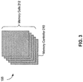
- Internal memory 106 includes a memory controller 210 and memory cells 212. Memory controller 210 controls access to memory cells 212. Memory cells 212 store data.
- internal memory 106 comprises an embedded, dynamic random access memory (DRAM).
- DRAM dynamic random access memory
- An embedded DRAM is a memory encapsulated in a common package with a processing unit.
- internal memory 106 comprises a stacked DRAM, as illustrated in FIG. 3 .
- a stacked memory includes a plurality of memory elements stacked on top of each other in a three-dimensional structure.
- Internal memory 106 is coupled to execution unit 142 via both input logic 202 and output logic 206.
- input logic 202 can retrieve data from internal memory 106
- output logic 206 can send data to internal memory 106 to be stored in memory cells 212.
- Internal memory 106 may also be coupled to the internal memory of another GPU via a first interface 250. Coupling internal memory 106 to the internal memory of another GPU can increase the total memory pool available to execution unit 142.
- first interface 250 provides dedicated access between internal memory 106 of GPU 110 and an internal memory of another GPU, as illustrated by interface 101 of FIG. 1A .
- first interface 250 is a provided on a standard pin of a conventional GPU.
- first interface 250 may comprise a display-controller interface, which provides a display device access to a local frame buffer included in internal memory 106.
- first interface 250 provides shared access between internal memory 106 of GPU 110 and internal memories of other processing units, as illustrated by interface 164 of FIG. 1B .
- Internal memory 106 may also be coupled to cache memory 130 of CPU 102 via a second interface 260. Accordingly, the combination of internal memory 106 and cache memory 130 can increase the memory pool available to GPU 110.
- second interface 260 provides a dedicated connection between internal memory 106 of GPU 110 and cache memory 130 of CPU 102, such as connection 103 or connection 105 of FIG. 1A .
- second interface 260 provides a connection that is shared by only GPU 110 and CPU 102, such as connection 164 of FIG. 1B .
- second interface couples GPU 110 to CPU 102 on a common bus, such as bus 114 of FIGS. 1A and 1B .
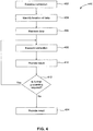
- FIG. 4 illustrates an example method 400 implemented by GPU 110 in accordance with an embodiment of the present invention. Method 400 is described below with reference to FIGS. 3 and 4 .
- Method 400 begins at a step 402 in which instruction are received.
- input logic 202 receives instructions to be executed by GPU 110.
- the instructions may comprise, for example, a graphics-processing task or a data-parallel processing task provided by an end-user application running on CPU 102 of system 100.
- a location of data associated with an instruction is identified.
- the data may be included with a received instruction. Such data is commonly referred to as immediate data.
- the instruction provides the location of the data.
- the instruction may include an address within which the data is stored.
- the instruction includes information from which input logic 202 computes the address within which the data is stored.
- the data may be stored in either internal memory 106, an internal memory of another GPU to which internal memory 106 is coupled, or cache memory 130 of CPU 102.
- the data is retrieved. If the data is immediate data, input logic 202 simply extracts the immediate data from the instruction. If the data is stored in internal memory 106 or a memory to which internal memory 106 is coupled, input logic 202 sends a request to memory controller 210 for access to the data. If, on the one hand, the data is stored in memory cells 212, the data is retrieved and provided to input logic 202. If, on the other hand, the data is stored in another memory coupled to internal memory 106, the request from input logic 202 is forwarded to the other memory via interface 250 or interface 260. The data is then retrieved from the other memory and provided to input logic 202.
- shader core 204 executes the instruction based on the data obtained by input logic 202 in step 406.
- results of the instruction execution are provided to output logic 206.
- Output logic 206 determines whether further processing is required on these results, as indicated in decision step 412.
- Results provides to output logic 206 may have a flag or some other indicia to indicate whether additional processing is necessary. If in decision step 412 output logic 206 determines that further processing is necessary, then output logic 206 forwards the results back to shader core 204 and steps 408 and 410 of method 400 are repeated. If, on the other hand, output logic 206 determines, in decision step 412, that no further processing is necessary, then output logic 206 provides the results to internal memory 106, as indicated in step 414.
- the results may then be written to internal memory 106 or to a memory coupled to internal memory 106, depending on the address to which the results are to be written. If the results are to be written to internal memory 106, memory controller 210 provides access to the appropriate address in memory cells 212 and the results are stored therein. If, on the other hand, the results are to be written to a memory coupled to internal memory 106, then memory controller 210 forwards the results to the other memory via interface 250 or interface 260 and the results are stored in memory cells of the other memory.
- GPUs may also be embodied in software disposed, for example, in a computer-readable medium configured to store the software (e.g., a computer-readable program code).
- the computer-readable program code enables embodiments of the present invention, including the following embodiments: (i) the functions of the systems and techniques disclosed herein (such as, providing tasks to GPU 110, scheduling tasks in GPU 110, executing tasks in GPU 110, or the like); (ii) the fabrication of the systems and techniques disclosed herein (such as, the fabrication of GPU 110); or (iii) a combination of the functions and fabrication of the systems and techniques disclosed herein.
- the computer-readable program code can be disposed in any known computer-readable medium including semiconductor, magnetic disk, or optical disk (such as CD-ROM, DVD-ROM). As such, the computer-readable program code can be transmitted over communication networks including the Internet and internets. It is understood that the functions accomplished and/or structure provided by the systems and techniques described above can be represented in a core (such as a shader core) that is embodied in computer-readable program code and may be transformed to hardware as part of the production of integrated circuits.
- a core such as a shader core
Landscapes
- Engineering & Computer Science (AREA)
- Software Systems (AREA)
- Theoretical Computer Science (AREA)
- Physics & Mathematics (AREA)
- General Engineering & Computer Science (AREA)
- General Physics & Mathematics (AREA)
- Memory System Of A Hierarchy Structure (AREA)
- Advance Control (AREA)
- Dram (AREA)
- Image Input (AREA)
- Image Processing (AREA)
- Multi Processors (AREA)
Applications Claiming Priority (3)
| Application Number | Priority Date | Filing Date | Title |
|---|---|---|---|
| US23973009P | 2009-09-03 | 2009-09-03 | |
| US12/616,636 US8803897B2 (en) | 2009-09-03 | 2009-11-11 | Internal, processing-unit memory for general-purpose use |
| PCT/US2010/047784 WO2011028984A1 (en) | 2009-09-03 | 2010-09-03 | An internal, processing-unit memory for general-purpose use |
Publications (2)
| Publication Number | Publication Date |
|---|---|
| EP2473915A1 EP2473915A1 (en) | 2012-07-11 |
| EP2473915B1 true EP2473915B1 (en) | 2017-03-15 |
Family
ID=43624191
Family Applications (1)
| Application Number | Title | Priority Date | Filing Date |
|---|---|---|---|
| EP10754627.7A Active EP2473915B1 (en) | 2009-09-03 | 2010-09-03 | An internal processing-unit memory for general-purpose use |
Country Status (7)
| Country | Link |
|---|---|
| US (1) | US8803897B2 (enExample) |
| EP (1) | EP2473915B1 (enExample) |
| JP (1) | JP2013504130A (enExample) |
| KR (1) | KR20120059590A (enExample) |
| CN (1) | CN102597951B (enExample) |
| IN (1) | IN2012DN02568A (enExample) |
| WO (1) | WO2011028984A1 (enExample) |
Families Citing this family (15)
| Publication number | Priority date | Publication date | Assignee | Title |
|---|---|---|---|---|
| US9058675B2 (en) * | 2010-05-29 | 2015-06-16 | Intel Corporation | Non-volatile storage for graphics hardware |
| US8819378B2 (en) * | 2011-11-14 | 2014-08-26 | Arm Limited | Data processing apparatus and method for performing memory transactions within such a data processing apparatus |
| US9239793B2 (en) | 2011-12-13 | 2016-01-19 | Ati Technologies Ulc | Mechanism for using a GPU controller for preloading caches |
| US20130163195A1 (en) * | 2011-12-22 | 2013-06-27 | Nvidia Corporation | System, method, and computer program product for performing operations on data utilizing a computation module |
| US8650525B2 (en) * | 2012-06-22 | 2014-02-11 | Altera Corporation | Integrated circuit compilation |
| CN103795947B (zh) * | 2012-10-31 | 2017-02-08 | 晨星软件研发(深圳)有限公司 | 使用在视频信号处理装置中的存储器空间配置方法 |
| US8884906B2 (en) * | 2012-12-21 | 2014-11-11 | Intel Corporation | Offloading touch processing to a graphics processor |
| JP6337494B2 (ja) * | 2013-07-08 | 2018-06-06 | 株式会社リコー | 画像処理装置、画像処理方法、及びプログラム |
| WO2015101827A1 (en) * | 2013-12-31 | 2015-07-09 | Mosys, Inc. | Integrated main memory and coprocessor with low latency |
| US10802995B2 (en) * | 2018-07-26 | 2020-10-13 | Xilinx, Inc. | Unified address space for multiple hardware accelerators using dedicated low latency links |
| CN110825530B (zh) * | 2018-08-10 | 2022-12-23 | 昆仑芯(北京)科技有限公司 | 用于人工智能芯片的指令执行方法和装置 |
| US11138135B2 (en) * | 2018-09-20 | 2021-10-05 | Samsung Electronics Co., Ltd. | Scale-out high bandwidth memory system |
| KR102693213B1 (ko) * | 2018-11-30 | 2024-08-09 | 에스케이하이닉스 주식회사 | 메모리 시스템 |
| EP4405774A4 (en) * | 2021-09-22 | 2025-05-21 | INTEL Corporation | Controlling a power consumption of circuitry |
| CN113867963A (zh) * | 2021-09-30 | 2021-12-31 | 联想(北京)有限公司 | 一种电子设备及处理方法 |
Citations (3)
| Publication number | Priority date | Publication date | Assignee | Title |
|---|---|---|---|---|
| US6956579B1 (en) * | 2003-08-18 | 2005-10-18 | Nvidia Corporation | Private addressing in a multi-processor graphics processing system |
| US20070294458A1 (en) * | 2006-06-15 | 2007-12-20 | Radoslav Danilak | Bus interface controller for cost-effective high performance graphics system with two or more graphics processing units |
| US20090077320A1 (en) * | 2004-10-08 | 2009-03-19 | Hoover Russell D | Direct access of cache lock set data without backing memory |
Family Cites Families (26)
| Publication number | Priority date | Publication date | Assignee | Title |
|---|---|---|---|---|
| EP0843254A3 (en) * | 1990-01-18 | 1999-08-18 | National Semiconductor Corporation | Integrated digital signal processor/general purpose CPU with shared internal memory |
| JPH05173941A (ja) * | 1991-12-26 | 1993-07-13 | Fujitsu Ltd | 並列計算機の分散フレームメモリによる画像処理装置 |
| JP4783527B2 (ja) * | 2001-01-31 | 2011-09-28 | 株式会社ガイア・システム・ソリューション | データ処理システム、データ処理装置およびその制御方法 |
| US6947051B2 (en) * | 2003-02-18 | 2005-09-20 | Microsoft Corporation | Video memory management |
| FR2865291A1 (fr) * | 2004-01-21 | 2005-07-22 | Thomson Licensing Sa | Procede de transfert de donnees dans un systeme multiprocesseur, systeme multiprocesseur et processeur mettant en oeuvre ce procede |
| JP2005296065A (ja) * | 2004-04-06 | 2005-10-27 | Konica Minolta Medical & Graphic Inc | 医用画像生成システム及び医用画像生成方法並びに表示制御プログラム |
| US7921365B2 (en) * | 2005-02-15 | 2011-04-05 | Microsoft Corporation | System and method for browsing tabbed-heterogeneous windows |
| JP2006268809A (ja) * | 2005-03-24 | 2006-10-05 | Kaadeikku Corporation:Kk | 画像メモリ並列回路 |
| US7522168B2 (en) * | 2005-09-27 | 2009-04-21 | Sony Computer Entertainment Inc. | Cell processor task and data management |
| TWI322354B (en) * | 2005-10-18 | 2010-03-21 | Via Tech Inc | Method and system for deferred command issuing in a computer system |
| US7376795B2 (en) * | 2005-10-27 | 2008-05-20 | International Business Machines Corporation | Memory coherence protocol enhancement using cache line access frequencies |
| US7965898B2 (en) * | 2005-10-28 | 2011-06-21 | Nvidia Corporation | Accelerating video decoding using multiple processors |
| US7500041B2 (en) * | 2006-06-15 | 2009-03-03 | Nvidia Corporation | Graphics processing unit for cost effective high performance graphics system with two or more graphics processing units |
| US7562174B2 (en) * | 2006-06-15 | 2009-07-14 | Nvidia Corporation | Motherboard having hard-wired private bus between graphics cards |
| US7619629B1 (en) * | 2006-06-15 | 2009-11-17 | Nvidia Corporation | Method and system for utilizing memory interface bandwidth to connect multiple graphics processing units |
| US7814486B2 (en) * | 2006-06-20 | 2010-10-12 | Google Inc. | Multi-thread runtime system |
| US20080109795A1 (en) * | 2006-11-02 | 2008-05-08 | Nvidia Corporation | C/c++ language extensions for general-purpose graphics processing unit |
| KR100813625B1 (ko) * | 2006-11-15 | 2008-03-14 | 삼성전자주식회사 | 반도체 소자 패키지 |
| US8271252B2 (en) * | 2007-11-08 | 2012-09-18 | Nvidia Corporation | Automatic verification of device models |
| US8335122B2 (en) * | 2007-11-21 | 2012-12-18 | The Regents Of The University Of Michigan | Cache memory system for a data processing apparatus |
| US8106914B2 (en) * | 2007-12-07 | 2012-01-31 | Nvidia Corporation | Fused multiply-add functional unit |
| US7836257B2 (en) * | 2007-12-19 | 2010-11-16 | International Business Machines Corpation | System and method for cache line replacement selection in a multiprocessor environment |
| US7925836B2 (en) * | 2008-01-25 | 2011-04-12 | Arm Limited | Selective coherency control |
| KR101619847B1 (ko) * | 2008-07-16 | 2016-05-11 | 삼성전자주식회사 | 화상형성장치, 호스트 장치 및 그의 웹페이지 인쇄 방법 |
| US8610732B2 (en) * | 2008-12-11 | 2013-12-17 | Nvidia Corporation | System and method for video memory usage for general system application |
| JP2011048579A (ja) * | 2009-08-26 | 2011-03-10 | Univ Of Tokyo | 画像処理装置及び画像処理方法 |
-
2009
- 2009-11-11 US US12/616,636 patent/US8803897B2/en active Active
-
2010
- 2010-09-03 IN IN2568DEN2012 patent/IN2012DN02568A/en unknown
- 2010-09-03 WO PCT/US2010/047784 patent/WO2011028984A1/en not_active Ceased
- 2010-09-03 CN CN201080049244.9A patent/CN102597951B/zh active Active
- 2010-09-03 KR KR1020127008022A patent/KR20120059590A/ko not_active Ceased
- 2010-09-03 EP EP10754627.7A patent/EP2473915B1/en active Active
- 2010-09-03 JP JP2012528080A patent/JP2013504130A/ja active Pending
Patent Citations (3)
| Publication number | Priority date | Publication date | Assignee | Title |
|---|---|---|---|---|
| US6956579B1 (en) * | 2003-08-18 | 2005-10-18 | Nvidia Corporation | Private addressing in a multi-processor graphics processing system |
| US20090077320A1 (en) * | 2004-10-08 | 2009-03-19 | Hoover Russell D | Direct access of cache lock set data without backing memory |
| US20070294458A1 (en) * | 2006-06-15 | 2007-12-20 | Radoslav Danilak | Bus interface controller for cost-effective high performance graphics system with two or more graphics processing units |
Also Published As
| Publication number | Publication date |
|---|---|
| KR20120059590A (ko) | 2012-06-08 |
| CN102597951A (zh) | 2012-07-18 |
| EP2473915A1 (en) | 2012-07-11 |
| WO2011028984A1 (en) | 2011-03-10 |
| IN2012DN02568A (enExample) | 2015-08-28 |
| JP2013504130A (ja) | 2013-02-04 |
| US20110050710A1 (en) | 2011-03-03 |
| CN102597951B (zh) | 2016-05-04 |
| US8803897B2 (en) | 2014-08-12 |
Similar Documents
| Publication | Publication Date | Title |
|---|---|---|
| EP2473915B1 (en) | An internal processing-unit memory for general-purpose use | |
| KR101661720B1 (ko) | 복수의 셰이더 엔진들을 구비한 처리 유닛 | |
| US9547535B1 (en) | Method and system for providing shared memory access to graphics processing unit processes | |
| US9965392B2 (en) | Managing coherent memory between an accelerated processing device and a central processing unit | |
| US9946666B2 (en) | Coalescing texture access and load/store operations | |
| US9269122B2 (en) | First and second software stacks and discrete and integrated graphics processing units | |
| US11908039B2 (en) | Graphics rendering method and apparatus, and computer-readable storage medium | |
| US9239793B2 (en) | Mechanism for using a GPU controller for preloading caches | |
| KR102521654B1 (ko) | 컴퓨팅 시스템 및 컴퓨팅 시스템에서 타일-기반 렌더링의 그래픽스 파이프라인을 수행하는 방법 | |
| EP4231242A1 (en) | Graphics rendering method and related device thereof | |
| US9710403B2 (en) | Power saving method and apparatus for first in first out (FIFO) memories | |
| US9864638B2 (en) | Techniques for accessing a graphical processing unit memory by an application | |
| US10672099B2 (en) | Memory cache management for graphics processing | |
| US9165337B2 (en) | Command instruction management | |
| CN117194055B (zh) | Gpu显存申请及释放的方法、装置及存储介质 | |
| US11372756B2 (en) | Memory pool management | |
| US20120013629A1 (en) | Reading Compressed Anti-Aliased Images | |
| US20250363063A1 (en) | Reserving a secure address range | |
| US8826294B2 (en) | Efficient state management system | |
| KR102223446B1 (ko) | 비특권 애플리케이션에 의한 그래픽 작업부하 실행의뢰 | |
| CN111625281A (zh) | 一种数据处理方法、装置、设备及存储介质 | |
| US20130262814A1 (en) | Mapping Memory Instructions into a Shared Memory Address Place | |
| US20210081328A1 (en) | Unified kernel virtual address space for heterogeneous computing | |
| US20150039867A1 (en) | Instruction source specification | |
| US11403223B2 (en) | De-prioritization supporting frame buffer caching |
Legal Events
| Date | Code | Title | Description |
|---|---|---|---|
| PUAI | Public reference made under article 153(3) epc to a published international application that has entered the european phase |
Free format text: ORIGINAL CODE: 0009012 |
|
| 17P | Request for examination filed |
Effective date: 20120308 |
|
| AK | Designated contracting states |
Kind code of ref document: A1 Designated state(s): AL AT BE BG CH CY CZ DE DK EE ES FI FR GB GR HR HU IE IS IT LI LT LU LV MC MK MT NL NO PL PT RO SE SI SK SM TR |
|
| DAX | Request for extension of the european patent (deleted) | ||
| 17Q | First examination report despatched |
Effective date: 20151019 |
|
| REG | Reference to a national code |
Ref country code: DE Ref legal event code: R079 Ref document number: 602010040780 Country of ref document: DE Free format text: PREVIOUS MAIN CLASS: G06F0009380000 Ipc: G06F0009500000 |
|
| GRAP | Despatch of communication of intention to grant a patent |
Free format text: ORIGINAL CODE: EPIDOSNIGR1 |
|
| RIC1 | Information provided on ipc code assigned before grant |
Ipc: G06F 9/54 20060101ALI20160909BHEP Ipc: G06F 9/38 20060101ALI20160909BHEP Ipc: G06F 9/50 20060101AFI20160909BHEP Ipc: G06F 9/46 20060101ALI20160909BHEP |
|
| INTG | Intention to grant announced |
Effective date: 20161006 |
|
| GRAS | Grant fee paid |
Free format text: ORIGINAL CODE: EPIDOSNIGR3 |
|
| GRAA | (expected) grant |
Free format text: ORIGINAL CODE: 0009210 |
|
| AK | Designated contracting states |
Kind code of ref document: B1 Designated state(s): AL AT BE BG CH CY CZ DE DK EE ES FI FR GB GR HR HU IE IS IT LI LT LU LV MC MK MT NL NO PL PT RO SE SI SK SM TR |
|
| REG | Reference to a national code |
Ref country code: CH Ref legal event code: EP Ref country code: GB Ref legal event code: FG4D |
|
| REG | Reference to a national code |
Ref country code: IE Ref legal event code: FG4D |
|
| REG | Reference to a national code |
Ref country code: AT Ref legal event code: REF Ref document number: 876220 Country of ref document: AT Kind code of ref document: T Effective date: 20170415 |
|
| REG | Reference to a national code |
Ref country code: DE Ref legal event code: R096 Ref document number: 602010040780 Country of ref document: DE |
|
| REG | Reference to a national code |
Ref country code: NL Ref legal event code: MP Effective date: 20170315 |
|
| REG | Reference to a national code |
Ref country code: LT Ref legal event code: MG4D |
|
| PG25 | Lapsed in a contracting state [announced via postgrant information from national office to epo] |
Ref country code: NO Free format text: LAPSE BECAUSE OF FAILURE TO SUBMIT A TRANSLATION OF THE DESCRIPTION OR TO PAY THE FEE WITHIN THE PRESCRIBED TIME-LIMIT Effective date: 20170615 Ref country code: FI Free format text: LAPSE BECAUSE OF FAILURE TO SUBMIT A TRANSLATION OF THE DESCRIPTION OR TO PAY THE FEE WITHIN THE PRESCRIBED TIME-LIMIT Effective date: 20170315 Ref country code: GR Free format text: LAPSE BECAUSE OF FAILURE TO SUBMIT A TRANSLATION OF THE DESCRIPTION OR TO PAY THE FEE WITHIN THE PRESCRIBED TIME-LIMIT Effective date: 20170616 Ref country code: HR Free format text: LAPSE BECAUSE OF FAILURE TO SUBMIT A TRANSLATION OF THE DESCRIPTION OR TO PAY THE FEE WITHIN THE PRESCRIBED TIME-LIMIT Effective date: 20170315 Ref country code: LT Free format text: LAPSE BECAUSE OF FAILURE TO SUBMIT A TRANSLATION OF THE DESCRIPTION OR TO PAY THE FEE WITHIN THE PRESCRIBED TIME-LIMIT Effective date: 20170315 |
|
| REG | Reference to a national code |
Ref country code: AT Ref legal event code: MK05 Ref document number: 876220 Country of ref document: AT Kind code of ref document: T Effective date: 20170315 |
|
| PG25 | Lapsed in a contracting state [announced via postgrant information from national office to epo] |
Ref country code: LV Free format text: LAPSE BECAUSE OF FAILURE TO SUBMIT A TRANSLATION OF THE DESCRIPTION OR TO PAY THE FEE WITHIN THE PRESCRIBED TIME-LIMIT Effective date: 20170315 Ref country code: SE Free format text: LAPSE BECAUSE OF FAILURE TO SUBMIT A TRANSLATION OF THE DESCRIPTION OR TO PAY THE FEE WITHIN THE PRESCRIBED TIME-LIMIT Effective date: 20170315 Ref country code: BG Free format text: LAPSE BECAUSE OF FAILURE TO SUBMIT A TRANSLATION OF THE DESCRIPTION OR TO PAY THE FEE WITHIN THE PRESCRIBED TIME-LIMIT Effective date: 20170615 |
|
| PG25 | Lapsed in a contracting state [announced via postgrant information from national office to epo] |
Ref country code: NL Free format text: LAPSE BECAUSE OF FAILURE TO SUBMIT A TRANSLATION OF THE DESCRIPTION OR TO PAY THE FEE WITHIN THE PRESCRIBED TIME-LIMIT Effective date: 20170315 |
|
| PG25 | Lapsed in a contracting state [announced via postgrant information from national office to epo] |
Ref country code: RO Free format text: LAPSE BECAUSE OF FAILURE TO SUBMIT A TRANSLATION OF THE DESCRIPTION OR TO PAY THE FEE WITHIN THE PRESCRIBED TIME-LIMIT Effective date: 20170315 Ref country code: EE Free format text: LAPSE BECAUSE OF FAILURE TO SUBMIT A TRANSLATION OF THE DESCRIPTION OR TO PAY THE FEE WITHIN THE PRESCRIBED TIME-LIMIT Effective date: 20170315 Ref country code: SK Free format text: LAPSE BECAUSE OF FAILURE TO SUBMIT A TRANSLATION OF THE DESCRIPTION OR TO PAY THE FEE WITHIN THE PRESCRIBED TIME-LIMIT Effective date: 20170315 Ref country code: CZ Free format text: LAPSE BECAUSE OF FAILURE TO SUBMIT A TRANSLATION OF THE DESCRIPTION OR TO PAY THE FEE WITHIN THE PRESCRIBED TIME-LIMIT Effective date: 20170315 Ref country code: AT Free format text: LAPSE BECAUSE OF FAILURE TO SUBMIT A TRANSLATION OF THE DESCRIPTION OR TO PAY THE FEE WITHIN THE PRESCRIBED TIME-LIMIT Effective date: 20170315 Ref country code: IT Free format text: LAPSE BECAUSE OF FAILURE TO SUBMIT A TRANSLATION OF THE DESCRIPTION OR TO PAY THE FEE WITHIN THE PRESCRIBED TIME-LIMIT Effective date: 20170315 Ref country code: ES Free format text: LAPSE BECAUSE OF FAILURE TO SUBMIT A TRANSLATION OF THE DESCRIPTION OR TO PAY THE FEE WITHIN THE PRESCRIBED TIME-LIMIT Effective date: 20170315 |
|
| PG25 | Lapsed in a contracting state [announced via postgrant information from national office to epo] |
Ref country code: IS Free format text: LAPSE BECAUSE OF FAILURE TO SUBMIT A TRANSLATION OF THE DESCRIPTION OR TO PAY THE FEE WITHIN THE PRESCRIBED TIME-LIMIT Effective date: 20170715 Ref country code: SM Free format text: LAPSE BECAUSE OF FAILURE TO SUBMIT A TRANSLATION OF THE DESCRIPTION OR TO PAY THE FEE WITHIN THE PRESCRIBED TIME-LIMIT Effective date: 20170315 Ref country code: PL Free format text: LAPSE BECAUSE OF FAILURE TO SUBMIT A TRANSLATION OF THE DESCRIPTION OR TO PAY THE FEE WITHIN THE PRESCRIBED TIME-LIMIT Effective date: 20170315 Ref country code: PT Free format text: LAPSE BECAUSE OF FAILURE TO SUBMIT A TRANSLATION OF THE DESCRIPTION OR TO PAY THE FEE WITHIN THE PRESCRIBED TIME-LIMIT Effective date: 20170717 |
|
| REG | Reference to a national code |
Ref country code: DE Ref legal event code: R097 Ref document number: 602010040780 Country of ref document: DE |
|
| PLBE | No opposition filed within time limit |
Free format text: ORIGINAL CODE: 0009261 |
|
| STAA | Information on the status of an ep patent application or granted ep patent |
Free format text: STATUS: NO OPPOSITION FILED WITHIN TIME LIMIT |
|
| PG25 | Lapsed in a contracting state [announced via postgrant information from national office to epo] |
Ref country code: DK Free format text: LAPSE BECAUSE OF FAILURE TO SUBMIT A TRANSLATION OF THE DESCRIPTION OR TO PAY THE FEE WITHIN THE PRESCRIBED TIME-LIMIT Effective date: 20170315 |
|
| 26N | No opposition filed |
Effective date: 20171218 |
|
| PG25 | Lapsed in a contracting state [announced via postgrant information from national office to epo] |
Ref country code: SI Free format text: LAPSE BECAUSE OF FAILURE TO SUBMIT A TRANSLATION OF THE DESCRIPTION OR TO PAY THE FEE WITHIN THE PRESCRIBED TIME-LIMIT Effective date: 20170315 |
|
| REG | Reference to a national code |
Ref country code: CH Ref legal event code: PL |
|
| PG25 | Lapsed in a contracting state [announced via postgrant information from national office to epo] |
Ref country code: MC Free format text: LAPSE BECAUSE OF FAILURE TO SUBMIT A TRANSLATION OF THE DESCRIPTION OR TO PAY THE FEE WITHIN THE PRESCRIBED TIME-LIMIT Effective date: 20170315 |
|
| REG | Reference to a national code |
Ref country code: IE Ref legal event code: MM4A |
|
| REG | Reference to a national code |
Ref country code: BE Ref legal event code: MM Effective date: 20170930 |
|
| PG25 | Lapsed in a contracting state [announced via postgrant information from national office to epo] |
Ref country code: LU Free format text: LAPSE BECAUSE OF NON-PAYMENT OF DUE FEES Effective date: 20170903 |
|
| REG | Reference to a national code |
Ref country code: FR Ref legal event code: ST Effective date: 20180531 |
|
| PG25 | Lapsed in a contracting state [announced via postgrant information from national office to epo] |
Ref country code: CH Free format text: LAPSE BECAUSE OF NON-PAYMENT OF DUE FEES Effective date: 20170930 Ref country code: IE Free format text: LAPSE BECAUSE OF NON-PAYMENT OF DUE FEES Effective date: 20170903 Ref country code: LI Free format text: LAPSE BECAUSE OF NON-PAYMENT OF DUE FEES Effective date: 20170930 |
|
| PG25 | Lapsed in a contracting state [announced via postgrant information from national office to epo] |
Ref country code: BE Free format text: LAPSE BECAUSE OF NON-PAYMENT OF DUE FEES Effective date: 20170930 Ref country code: FR Free format text: LAPSE BECAUSE OF NON-PAYMENT OF DUE FEES Effective date: 20171002 |
|
| PG25 | Lapsed in a contracting state [announced via postgrant information from national office to epo] |
Ref country code: MT Free format text: LAPSE BECAUSE OF NON-PAYMENT OF DUE FEES Effective date: 20170903 |
|
| PG25 | Lapsed in a contracting state [announced via postgrant information from national office to epo] |
Ref country code: HU Free format text: LAPSE BECAUSE OF FAILURE TO SUBMIT A TRANSLATION OF THE DESCRIPTION OR TO PAY THE FEE WITHIN THE PRESCRIBED TIME-LIMIT; INVALID AB INITIO Effective date: 20100903 |
|
| PG25 | Lapsed in a contracting state [announced via postgrant information from national office to epo] |
Ref country code: CY Free format text: LAPSE BECAUSE OF NON-PAYMENT OF DUE FEES Effective date: 20170315 |
|
| PG25 | Lapsed in a contracting state [announced via postgrant information from national office to epo] |
Ref country code: MK Free format text: LAPSE BECAUSE OF FAILURE TO SUBMIT A TRANSLATION OF THE DESCRIPTION OR TO PAY THE FEE WITHIN THE PRESCRIBED TIME-LIMIT Effective date: 20170315 |
|
| PG25 | Lapsed in a contracting state [announced via postgrant information from national office to epo] |
Ref country code: TR Free format text: LAPSE BECAUSE OF FAILURE TO SUBMIT A TRANSLATION OF THE DESCRIPTION OR TO PAY THE FEE WITHIN THE PRESCRIBED TIME-LIMIT Effective date: 20170315 |
|
| PG25 | Lapsed in a contracting state [announced via postgrant information from national office to epo] |
Ref country code: AL Free format text: LAPSE BECAUSE OF FAILURE TO SUBMIT A TRANSLATION OF THE DESCRIPTION OR TO PAY THE FEE WITHIN THE PRESCRIBED TIME-LIMIT Effective date: 20170315 |
|
| P01 | Opt-out of the competence of the unified patent court (upc) registered |
Effective date: 20230530 |
|
| PGFP | Annual fee paid to national office [announced via postgrant information from national office to epo] |
Ref country code: DE Payment date: 20250819 Year of fee payment: 16 |
|
| PGFP | Annual fee paid to national office [announced via postgrant information from national office to epo] |
Ref country code: GB Payment date: 20250911 Year of fee payment: 16 |