EP2461353A2 - Cmp-polierkissen und verfahren zu seiner herstellung - Google Patents
Cmp-polierkissen und verfahren zu seiner herstellung Download PDFInfo
- Publication number
- EP2461353A2 EP2461353A2 EP10804606A EP10804606A EP2461353A2 EP 2461353 A2 EP2461353 A2 EP 2461353A2 EP 10804606 A EP10804606 A EP 10804606A EP 10804606 A EP10804606 A EP 10804606A EP 2461353 A2 EP2461353 A2 EP 2461353A2
- Authority
- EP
- European Patent Office
- Prior art keywords
- dyes
- polishing pad
- light
- cmp polishing
- holes
- Prior art date
- Legal status (The legal status is an assumption and is not a legal conclusion. Google has not performed a legal analysis and makes no representation as to the accuracy of the status listed.)
- Granted
Links
Images


Classifications
-
- B—PERFORMING OPERATIONS; TRANSPORTING
- B24—GRINDING; POLISHING
- B24D—TOOLS FOR GRINDING, BUFFING OR SHARPENING
- B24D18/00—Manufacture of grinding tools or other grinding devices, e.g. wheels, not otherwise provided for
-
- H10P52/00—
-
- B—PERFORMING OPERATIONS; TRANSPORTING
- B24—GRINDING; POLISHING
- B24B—MACHINES, DEVICES, OR PROCESSES FOR GRINDING OR POLISHING; DRESSING OR CONDITIONING OF ABRADING SURFACES; FEEDING OF GRINDING, POLISHING, OR LAPPING AGENTS
- B24B37/00—Lapping machines or devices; Accessories
- B24B37/11—Lapping tools
- B24B37/20—Lapping pads for working plane surfaces
- B24B37/26—Lapping pads for working plane surfaces characterised by the shape of the lapping pad surface, e.g. grooved
Definitions
- the present disclosure relates to a Chemical Mechanical Polishing (CMP) polishing pad and a method for manufacturing the same, and more particularly, to a CMP polishing pad having holes formed by laser beams on the surface thereof in order to improve the stability of a CMP process and a method for manufacturing the same.
- CMP Chemical Mechanical Polishing
- Semiconductors are devices obtained by high-density integration of electronic devices such as transistors or capacitors on a semiconductor substrate such as silicon, and are fabricated by using deposition, photolithography and etching technologies. Repetition of such deposition, photolithography and etching processes results in formation of a pattern having a specific shape. When the formation of patterns is repeated in a layered structure, a level difference gradually becomes severe at the top of the resultant structure. Such a severe level difference at the top of the structure makes the focus of a photomask pattern unclear in the subsequent photolithography process, thereby making it difficult to form a fine pattern.
- CMP Chemical Mechanical Polishing
- Fig. 1 is a schematic view illustrating a CMP process. Referring to Fig. 1 , the CMP process is carried out by allowing a wafer 103 to rotate while being in contact with a rotating CMP polishing pad 102 so that the layer formed on the top of a wafer 103 may be polished.
- the CMP polishing pad 102 is bound to a rotating flat table 101 and the wafer 103 is rotated while being in contact with the CMP polishing pad 102 by way of a carrier 104.
- slurry 106 is supplied from a slurry feed nozzle 105 to the top of the CMP polishing pad 102.
- CMP polishing pads are consumable goods for use in polishing wafer surfaces and are essential for CMP processes.
- the slurry is present between the CMP polishing pad and the wafer surface during CMP to carry put chemical mechanical polishing of the wafer surface. Then, the used slurry is discharged to the exterior.
- Such slurry storability of the CMP polishing pad may be obtained by pores or holes formed on the polishing pad. In other words, the slurry is introduced into the pores or holes formed on the CMP polishing pad so that the semiconductor surface may be polished efficiently for a long time.
- the shapes of the pores or holes are controlled well and the physical properties, such as hardness, of the polishing pad are maintained in an optimized condition.
- FIG. 2 is a sectional view showing a CMP polishing pad obtained according to the related art. Referring to Fig. 2 , pores 102a having various shapes and sizes are arranged in a randomly distributed form on the surface or inside of a polishing pad 102 made of polymer.
- One of the physical methods among the conventional methods for forming pores or holes on a CMP polishing pad is mixing a micro-sized material with a material for forming a polishing pad.
- a porous micro-sized material is placed in such a manner that it may be mixed well with a polishing pad material at the initial time of polishing pad fabrication.
- the micro-sized material is not uniform in size.
- the average pore diameter of pores formed by a physical method is about 100 micrometers, but each pore has a diameter ranging from several tens micrometers to several hundred micrometers.
- One of the chemical methods for forming pores on a CMP polishing pad uses water or liquid capable of being converted into gas.
- water or liquid capable of being converted into gas.
- pores are formed while the liquid is converted into gas.
- such a method for forming pores by using gas is still problematic in that maintenance of a uniform pore size is difficult. Therefore, there has been a need for developing a method for maintaining a uniform shape of the pores or holes formed on a CMP polishing pad and controlling the distribution of pores or holes as desired.
- the present disclosure is directed to providing a CMP polishing pad having holes formed on the surface thereof, wherein the holes have a diameter controlled to a predetermined size.
- the present disclosure is also directed to providing a method for manufacturing a CMP polishing pad having holes formed on the surface thereof, wherein the holes have a diameter controlled to a predetermined size.
- the present disclosure provides a CMP polishing pad having a plurality of holes formed on at least one surface thereof, wherein the holes are formed by dispersing a light-absorbing material in or on the surface of a CMP polishing pad and irradiating the light-absorbing material with laser beams.
- the holes may have a diameter determined by the wavelength of the laser beams.
- the diameter of the holes may be in proportion to the wavelength of the laser beams.
- the laser beams may have a median wavelength of 300-20,000 nm.
- the holes may have a diameter of 1-200 ⁇ m.
- the light-absorbing material may absorb light in a wavelength range of 300-15,000 nm.
- the light-absorbing material may be at least one material selected from the group comprising cyanine dyes, dithiolene dyes, diimmonium dyes, quinone dyes, rhodamine dyes, victoria dyes, methylene dyes, brilliant dyes, naphthalene dyes, repid-filter gelb, echtblau, pinaorthol dyes, pyrylium dyes, thionin dyes, nile blue dyes, cresyl dyes, oxazine dyes, resorufin dyes, resazurin dyes, pyronin dyes, acridine dyes and kiton dyes.
- cyanine dyes dithiolene dyes, diimmonium dyes, quinone dyes, rhodamine dyes, victoria dyes, methylene dyes, brilliant dyes, naphthalene dyes, repid-filter gelb, echtblau, pinaorthol
- a CMP polishing pad having a plurality of holes generated by forming a light-absorbing material layer on the surface of the polishing pad and irradiating the light-absorbing material layer with laser beams so that the laser beams penetrate through the light-absorbing material layer and the holes are formed to a predetermined depth of the polishing pad.
- the light-absorbing material layer may be formed by spreading a light-absorbing material onto the surface of the polishing pad or by attaching a film having a light-absorbing material dispersed therein to the surface of the polishing pad.
- the present disclosure provides a method for manufacturing a CMP polishing pad, including: determining a diameter of holes to be formed on a CMP polishing pad; determining a particular type of laser to be used according to the diameter of holes; determining a particular type of light-absorbing material according to the type of laser; dispersing the light-absorbing material in the CMP polishing pad; and irradiating the CMP polishing pad having the light-absorbing material dispersed therein with the laser beams to form holes.
- the diameter of holes may be in proportion to the wavelength of laser beams.
- the light-absorbing material may be at least one material selected from the group comprising cyanine dyes, dithiolene dyes, diimmonium dyes, quinone dyes, rhodamine dyes, victoria dyes, methylene dyes, brilliant dyes, naphthalene dyes, repid-filter gelb, echtblau, pinaorthol dyes, pyrylium dyes, thionin dyes, nile blue dyes, cresyl dyes, oxazine dyes, resorufin dyes, resazurin dyes, pyronin dyes, acridine dyes and kiton dyes.
- cyanine dyes dithiolene dyes, diimmonium dyes, quinone dyes, rhodamine dyes, victoria dyes, methylene dyes, brilliant dyes, naphthalene dyes, repid-filter gelb, echtblau, pinaorthol
- a plurality of holes is to be formed on the CMP polishing pad, and the distribution and depth of the holes may be controlled by varying the position of the polishing pad.
- a plurality of holes is to be formed on the CMP polishing pad, and the distribution and depth of the holes may be controlled by varying the position of the laser.
- the CMP polishing pad disclosed herein uses a light-absorbing material capable of absorbing light in a specific range of wavelengths on the surface thereof or therein, and thus allows formation of holes using laser beams. Therefore, it is possible to form holes having a desired diameter effectively on the CMP polishing pad by selecting the wavelength of laser beams and the light-absorbing material corresponding thereto according to the diameter of holes to be formed. In addition, since the holes are formed by laser beams, they may have a desired depth and distribution in the polishing pad. Further, it is possible to carry out a CMP process with high polishing efficiency and high process stability, depending on the type of a material to be polished or the composition of slurry.
- the CMP polishing pad disclosed herein has a plurality of holes formed on at least one surface thereof, wherein the holes are formed by dispersing a light-absorbing material in or on the surface of a CMP polishing pad and irradiating the light-absorbing material with laser beams.
- the holes are formed by laser beams, and have a diameter determined by the wavelength of the laser beams.
- the holes formed with a uniform diameter on the CMP polishing pad allow the CMP polishing pad to retain slurry for a predetermined time, thereby ensuring high CMP efficiency and process stability.
- Such formation of holes using laser beams is accomplished by irradiating the polishing pad with strong laser beams having a range of wavelengths capable of being absorbed by the CMP polishing pad so that the materials forming the polishing pad may be molten partially.
- Fig. 3 is a schematic view showing a method for forming holes with a desired distribution and depth on a CMP polishing pad by using a laser.
- the distribution and depth of the holes to be formed on the polishing pad are determined first, and then they are programmed so that a laser unit or a mobile mechanism attached to the CMP polishing pad may be controlled by a computer numerical control (CNC) process. In this manner, it is possible to control the distribution and depth of the holes.
- the distribution of the holes formed on the CMP polishing pad is controlled by moving the laser unit or mobile mechanism in the horizontal direction, while the depth of the holes is controlled by the intensity or exposure time of the laser beams or by moving the laser unit or mobile mechanism in the vertical direction.
- Fig. 4 is a sectional view showing a CMP polishing pad having holes formed to a predetermined depth by using laser beams. Referring to Fig. 4 , holes having a uniform diameter are formed on the top surface of the CMP polishing pad to a uniform depth. Although the holes shown in Fig. 4 have the same depth and same interval, it is also possible to form holes having various distribution patterns and different depths on the CMP polishing pad by controlling the horizontal and vertical movement of the laser unit or mobile mechanism.
- CMP polishing pads are made of polyurethane polymers, which have high absorbance to far IR rays and UV rays.
- use of carbon dioxide laser beams having a wavelength of 10.64 ⁇ m makes it difficult to control the diameter of holes to 100 ⁇ m or less due to the wavelength of the carbon dioxide laser beams.
- the CMP process using the pad provides poor polishing efficiency.
- UV laser beams having a smaller wavelength range than carbon dioxide laser beams are used instead of carbon dioxide laser beams, it is possible to control the diameter of the holes formed on the CMP polishing pad to an extent of several micrometers. However, in this case, it is still difficult to control the diameter to an extent of several tens micrometers. If the holes formed on the CMP polishing pad have a diameter as small as several micrometers, an excessively large number of holes are to be formed per unit area of the pad, resulting in an increase in processing time and degradation of production efficiency.
- the range of controllable hole diameters is in proportion to the wavelength range of laser beams. Therefore, laser units of near IR rays or visible rays may be used to form holes having a diameter of several tens micrometers on a CMP polishing pad. In this case, it is required for the materials forming the CMP polishing pad to absorb the light having the corresponding range of wavelengths.
- a light-absorbing material is dispersed in a CMP polishing pad.
- a light-absorbing material selected according to the wavelength of laser beams is dispersed on the surface of or inside a CMP polishing pad so that the light absorbance to a range of near IR rays to visible rays may be increased. In this manner, it is possible to form holes on a polishing pad more efficiently.
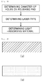
- Fig. 5 is a flow chart showing how to select a light-absorbing material to be dispersed on a CMP polishing pad according to the present disclosure.
- a diameter of holes to be formed on a polishing pad is determined first according to the particular type of a CMP process and that of a material to be polished.
- an adequate wavelength range of laser beams and a particular type of laser unit are determined according to the diameter of holes determined as mentioned above.
- determined is a light-absorbing material capable of absorbing the light corresponding to the thus determined wavelength range of laser beams.
- Polyurethane polymers used for forming CMP polishing pads have high absorbance to far IR rays and UV rays but their absorbance to the light corresponding to near IR rays and visible rays is not significantly high. Therefore, it is required to disperse a light-absorbing material capable of absorbing the light corresponding to near IR rays and visible rays on the surface of or in a polishing pad.
- Laser units generating light of a range of visible rays or near IR rays include GaAs lasers (0.83 ⁇ m), Nd-YAG lasers (1.06 ⁇ m) or HF lasers (2.8 ⁇ m). In addition to those lasers, various types of lasers capable of generating light of an adequate wavelength range may be used.
- the light-absorbing material may be selected according to the wavelength range of the light generated from a specific laser unit. Conventional dyes or organic or inorganic materials known to absorb the light of a specific wavelength range may be used. Particular examples of the light-absorbing material absorbing light of near IR wavelengths include cyanine dyes, dithiolene dyes, diimmonium dyes, quinone dyes, rhodamine dyes, victoria dyes, methylene dyes, brilliant dyes, naphthalene dyes, repid-filter gelb, echtblau, pinaorthol dyes, pyrylium dyes, thionin dyes, nile blue dyes, cresyl dyes, oxazine dyes, resorufin dyes, resazurin dyes, pyronin dyes, acridine dyes and kiton dyes. Particular examples of the cyanine dyes include phthalocyanine compounds, naphthalocyanine compounds, amino group
- dithiolene dyes include bis(dithiobenzyl) nickel complex compounds, bis(1,2-acenaphthylenedithilolite) nickel complex compounds, 4-tert-butyl-1,2-benzenedithiol nickel complex compounds, alkoxy group-containing bis(dithiobenzyl) nickel complex compounds, etc.
- dyes include bis(dithiobenzyl) nickel complex compounds, bis(1,2-acenaphthylenedithilolite) nickel complex compounds, 4-tert-butyl-1,2-benzenedithiol nickel complex compounds, alkoxy group-containing bis(dithiobenzyl) nickel complex compounds, etc.
- Diimmonium dyes absorbing light within a wavelength range of 0.95-1.1 ⁇ m may also be used as a light-absorbing material according to the present disclosure.
- Light-absorbing materials absorbing light of a wavelength ranges corresponding to visible rays include rhodamine dyes absorbing green light with a wavelength range of 0.5
- Fig. 6 is a sectional view showing a CMP polishing pad having a light-absorbing material dispersed therein according to an embodiment.
- the light-absorbing material may be incorporated to and dispersed in a polishing pad as shown in portion (a). Otherwise, the light-absorbing material may be dispersed uniformly inside the polishing pad in the form of particles as shown in portion (b).
- the light-absorbing material having high miscibility with a polyurethane polymer may be selected.
- the light-absorbing material when the light-absorbing material is dispersed in a polyurethane polymer in the form of particles as shown in portion (b), it is required for the light-absorbing material to be dispersed uniformly in order to maintain a uniform diameter of holes along the depth of the pad.
- a light-absorbing material in the form of particles is molten by itself in the presence of laser beams. Otherwise, even when the light-absorbing material is not molten, it transfers heat to the surroundings so that the polyurethane polymer may be molten.
- the particle may have a size controlled to 1/10 or less of the diameter of laser beams.
- the light-absorbing material may be dispersed on the surface of the CMP polishing pad.
- the light-absorbing material is dispersed in the polishing pad, it is miscible with the polyurethane polymer forming the polishing pad or it is dispersed uniformly in the polyurethane polymer in the form of particles.
- the particle-like light-absorbing material is distributed and dispersed predominantly on the surface of the polishing pad, or is applied to the surface of the polishing pad.
- the particle-like light-absorbing material When the particle-like light-absorbing material is distributed predominantly on the surface of the polishing pad, it is assumed that a higher proportion of the particle-like light-absorbing material is distributed on the bottom surface of the polishing pad due to the gravity during the fabrication of the polishing pad. This may be applied advantageously to formation of holes having a relatively small depth on the polishing pad.
- the other embodiment in which the light-absorbing material is applied to the surface of the polishing pad may be applied advantageously to dispersion of a light-absorbing material having low miscibility with the materials forming the polishing pad on the polishing pad.
- the light-absorbing material may be formed as a separate layer on the surface of the CMP polishing pad.
- Methods for forming a light-absorbing material as a separate layer on the CMP polishing pad include methods for spreading a light-absorbing material onto the polishing pad, and methods for coating a film containing a light-absorbing material on the polishing pad.
- the former may include spreading a light-absorbing material onto the surface of the polishing pad through a spin coating process, etc., spreading a solid-phase light-absorbing material onto the surface of the polishing pad through a vapor phase deposition process, or adding a particle-like light-absorbing material to a solution containing a polymer resin and a solvent and spreading the solution onto the surface of the polishing pad.
- the latter may include dispersing a light-absorbing material in a film and coating the film on the surface of the polishing pad, or spreading a light-absorbing material onto the surface of a film and coating the film on the surface of the polishing pad.
- the film may be formed of a polymer resin and may be coated on the polishing pad by using an adhesive or hot press.
- the light-absorbing material is formed as a separate layer on the surface of the polishing pad, laser beams irradiated to the polishing pad are absorbed first by the light-absorbing material formed on the polishing pad and then penetrate through the pad, so that holes are formed to a predetermined depth.
- a light-absorbing material formed as a separate layer on the surface of the CMP polishing pad increases light absorbance while not changing the intrinsic physical properties of the CMP polishing pad.
- Fig. 7 is a sectional view showing a CMP polishing pad having a light-absorbing material formed as a separate layer on the surface of the CMP polishing pad according to another embodiment.
- a light-absorbing material layer 302 is formed as a separate layer on the CMP polishing pad 301.
- the thickness of the light-absorbing material layer is exaggerated so that the light-absorbing material layer is differentiated clearly from the polishing pad.
- an adhesive layer (not shown) may be inserted between the light-absorbing material layer 302 and the polishing pad 301.
- Fig. 8 is a sectional view showing the holes formed on a CMP polishing pad having a light-absorbing material according to the present disclosure.
- holes having a diameter of 70 ⁇ m are formed on the CMP polishing pad to a depth of 2,000 ⁇ m. Therefore, it can be seen that holes having such a controlled diameter, which, otherwise, cannot be obtained easily according to the related art, are formed effectively on the CMP polishing pad by dispersing a light-absorbing material in the polishing pad.
- the diameter of the holes formed on the CMP polishing pad may be controlled within a wide range according to the particular type of CMP process and that of the material to be polished.
- the diameter of the holes formed on the CMP polishing pad may be 1-200 ⁇ m.
- the laser beams used for forming the holes may have a wavelength ranging from 300 nm to 20,000 nm.
- the light-absorbing material dispersed in the polishing pad may absorb the light within a wavelength range of 300 nm to 15,000 nm.
- the wavelength range of laser beams is determined considering the diameter of the holes formed on the CMP polishing pad.
- the absorption wavelength range of the light-absorbing material is determined in such a manner that it compensate for a deficiency in the light absorption wavelength range of a polyurethane polymer.
- the holes may be distributed in various manners.
- the holes may be arranged in a regular, random, chaos or fractal pattern, or a combination thereof.
- the arrangement of holes may be selected considering the material to be polished, particular type of slurry or wafer size, etc.
- the distribution of the holes formed on the CMP polishing pad may be realized in such a manner that a higher proportion of holes is present at the center and the number of holes gradually decreases toward the peripheral portion, or a smaller proportion of holes is present at the center and the number of holes gradually increases toward the peripheral portion.
- the former case provides the CMP polishing pad with lower hardness at the center thereof and allows slurry feed to be concentrated at the center.
- the latter case results in a contrary effect.
- the distribution of holes may be controlled diversely according to the pattern shape of a material subjected to CMP or the structure of a CMP system.
Landscapes
- Engineering & Computer Science (AREA)
- Mechanical Engineering (AREA)
- Manufacturing & Machinery (AREA)
- Mechanical Treatment Of Semiconductor (AREA)
- Finish Polishing, Edge Sharpening, And Grinding By Specific Grinding Devices (AREA)
Applications Claiming Priority (2)
| Application Number | Priority Date | Filing Date | Title |
|---|---|---|---|
| KR1020090069960A KR101044279B1 (ko) | 2009-07-30 | 2009-07-30 | Cmp 연마패드와 그의 제조방법 |
| PCT/KR2010/002728 WO2011013893A2 (ko) | 2009-07-30 | 2010-04-30 | Cmp 연마패드와 그의 제조방법 |
Publications (3)
| Publication Number | Publication Date |
|---|---|
| EP2461353A2 true EP2461353A2 (de) | 2012-06-06 |
| EP2461353A4 EP2461353A4 (de) | 2013-01-09 |
| EP2461353B1 EP2461353B1 (de) | 2015-09-09 |
Family
ID=43529791
Family Applications (1)
| Application Number | Title | Priority Date | Filing Date |
|---|---|---|---|
| EP10804606.1A Not-in-force EP2461353B1 (de) | 2009-07-30 | 2010-04-30 | Cmp-polierkissen und verfahren zu seiner herstellung |
Country Status (6)
| Country | Link |
|---|---|
| US (1) | US20120184194A1 (de) |
| EP (1) | EP2461353B1 (de) |
| JP (1) | JP5711739B2 (de) |
| KR (1) | KR101044279B1 (de) |
| CN (1) | CN102484058B (de) |
| WO (1) | WO2011013893A2 (de) |
Families Citing this family (3)
| Publication number | Priority date | Publication date | Assignee | Title |
|---|---|---|---|---|
| US10226853B2 (en) | 2013-01-18 | 2019-03-12 | Applied Materials, Inc. | Methods and apparatus for conditioning of chemical mechanical polishing pads |
| WO2015023442A1 (en) | 2013-08-10 | 2015-02-19 | Applied Materials, Inc. | Cmp pads having material composition that facilitates controlled conditioning |
| US20150044783A1 (en) * | 2013-08-12 | 2015-02-12 | Micron Technology, Inc. | Methods of alleviating adverse stress effects on a wafer, and methods of forming a semiconductor device |
Family Cites Families (20)
| Publication number | Priority date | Publication date | Assignee | Title |
|---|---|---|---|---|
| MY114512A (en) * | 1992-08-19 | 2002-11-30 | Rodel Inc | Polymeric substrate with polymeric microelements |
| EP0984846B1 (de) * | 1997-01-13 | 2004-11-24 | Rodel, Inc. | Verfahren zum herstellen von einem photolithographisch gemusterten kunststoffpolierkissen |
| US6039775A (en) * | 1997-11-03 | 2000-03-21 | 3M Innovative Properties Company | Abrasive article containing a grinding aid and method of making the same |
| JP2001071256A (ja) * | 1999-08-31 | 2001-03-21 | Shinozaki Seisakusho:Kk | 研磨パッドの溝形成方法及び装置並びに研磨パッド |
| US6652764B1 (en) * | 2000-08-31 | 2003-11-25 | Micron Technology, Inc. | Methods and apparatuses for making and using planarizing pads for mechanical and chemical-mechanical planarization of microelectronic substrates |
| US6380270B1 (en) * | 2000-09-26 | 2002-04-30 | Honeywell International Inc. | Photogenerated nanoporous materials |
| US7192340B2 (en) * | 2000-12-01 | 2007-03-20 | Toyo Tire & Rubber Co., Ltd. | Polishing pad, method of producing the same, and cushion layer for polishing pad |
| KR100497205B1 (ko) * | 2001-08-02 | 2005-06-23 | 에스케이씨 주식회사 | 마이크로홀이 형성된 화학적 기계적 연마패드 |
| EP1412129A4 (de) * | 2001-08-02 | 2008-04-02 | Skc Co Ltd | Verfahren zur herstellung eines chemisch-mechanischen polierkissens unter verwendung von laser |
| US7534498B2 (en) * | 2002-06-03 | 2009-05-19 | 3M Innovative Properties Company | Laminate body, method, and apparatus for manufacturing ultrathin substrate using the laminate body |
| JP3737787B2 (ja) * | 2002-07-16 | 2006-01-25 | 株式会社東芝 | 半導体装置の製造方法 |
| US20050196710A1 (en) * | 2004-03-04 | 2005-09-08 | Semiconductor Energy Laboratory Co., Ltd. | Method for forming pattern, thin film transistor, display device and method for manufacturing the same, and television apparatus |
| JP4868708B2 (ja) * | 2004-03-05 | 2012-02-01 | 日東電工株式会社 | レーザーダイシング・ダイボンド用粘着シート及びこれを用いた半導体装置の製造方法 |
| JP5288690B2 (ja) * | 2005-05-13 | 2013-09-11 | 東洋ゴム工業株式会社 | 研磨パッドの製造方法および研磨パッドの溝加工方法 |
| US20070235904A1 (en) * | 2006-04-06 | 2007-10-11 | Saikin Alan H | Method of forming a chemical mechanical polishing pad utilizing laser sintering |
| US8796125B2 (en) * | 2006-06-12 | 2014-08-05 | Kovio, Inc. | Printed, self-aligned, top gate thin film transistor |
| JP2008188661A (ja) * | 2007-02-07 | 2008-08-21 | Sumitomo Electric Ind Ltd | レーザ加工方法 |
| US8129098B2 (en) * | 2007-11-20 | 2012-03-06 | Eastman Kodak Company | Colored mask combined with selective area deposition |
| WO2009123659A1 (en) * | 2008-04-01 | 2009-10-08 | Innopad, Inc. | Polishing pad with controlled void formation |
| JP2010027952A (ja) * | 2008-07-23 | 2010-02-04 | Toshiba Corp | 半導体装置の製造方法 |
-
2009
- 2009-07-30 KR KR1020090069960A patent/KR101044279B1/ko not_active Expired - Fee Related
-
2010
- 2010-04-30 JP JP2012522742A patent/JP5711739B2/ja not_active Expired - Fee Related
- 2010-04-30 US US13/387,398 patent/US20120184194A1/en not_active Abandoned
- 2010-04-30 WO PCT/KR2010/002728 patent/WO2011013893A2/ko not_active Ceased
- 2010-04-30 EP EP10804606.1A patent/EP2461353B1/de not_active Not-in-force
- 2010-04-30 CN CN201080038956.0A patent/CN102484058B/zh not_active Expired - Fee Related
Also Published As
| Publication number | Publication date |
|---|---|
| WO2011013893A2 (ko) | 2011-02-03 |
| JP2013500600A (ja) | 2013-01-07 |
| JP5711739B2 (ja) | 2015-05-07 |
| US20120184194A1 (en) | 2012-07-19 |
| CN102484058B (zh) | 2015-06-17 |
| EP2461353A4 (de) | 2013-01-09 |
| EP2461353B1 (de) | 2015-09-09 |
| KR20110012293A (ko) | 2011-02-09 |
| KR101044279B1 (ko) | 2011-06-28 |
| CN102484058A (zh) | 2012-05-30 |
| WO2011013893A3 (ko) | 2011-03-24 |
Similar Documents
| Publication | Publication Date | Title |
|---|---|---|
| US20190009388A1 (en) | Uv curable cmp polishing pad and method of manufacture | |
| TWI687312B (zh) | 由積層製造製程所生產之研磨墊 | |
| TWI544984B (zh) | 研磨物件,其製備方法及其使用方法 | |
| KR100487455B1 (ko) | 사진석판술에 의해 유도된 표면 패턴(들)이 있는 연마용 중합체 패드 및 이에 관련된 방법 | |
| TW201726325A (zh) | 多孔化學機械研磨墊 | |
| US10773509B2 (en) | Pad structure and fabrication methods | |
| JP2007531638A (ja) | 研磨パッドおよびその製造方法 | |
| US20150044951A1 (en) | Cmp pads having material composition that facilitates controlled conditioning | |
| EP2461353B1 (de) | Cmp-polierkissen und verfahren zu seiner herstellung | |
| US8357027B2 (en) | Polishing pad and method of manufacture | |
| US20120178349A1 (en) | Cmp polishing pad having pores formed therein, and method for manufacturing same | |
| WO2021252537A1 (en) | Additive manufacturing of polishing pads | |
| KR101744694B1 (ko) | 혼합 기공 구조를 갖는 cmp패드 | |
| US20210379726A1 (en) | Additive Manufacturing of Polishing Pads | |
| KR20110002313A (ko) | 기공이 형성된 cmp 연마패드 및 기공의 형성방법 | |
| KR102832719B1 (ko) | 수직 방향 홈을 갖는 돌출 패턴을 포함하는 연마 패드, 그 제조 방법 및 연마 장치 | |
| KR101740748B1 (ko) | 분산된 기공 구조를 갖는 cmp패드 및 그 제조방법 | |
| JP2024141513A (ja) | 研磨パッド | |
| KR20180096125A (ko) | 혼합된 캐비티 구조를 갖는 cmp 공정용 연마 패드 |
Legal Events
| Date | Code | Title | Description |
|---|---|---|---|
| PUAI | Public reference made under article 153(3) epc to a published international application that has entered the european phase |
Free format text: ORIGINAL CODE: 0009012 |
|
| 17P | Request for examination filed |
Effective date: 20120208 |
|
| AK | Designated contracting states |
Kind code of ref document: A2 Designated state(s): AT BE BG CH CY CZ DE DK EE ES FI FR GB GR HR HU IE IS IT LI LT LU LV MC MK MT NL NO PL PT RO SE SI SK SM TR |
|
| DAX | Request for extension of the european patent (deleted) | ||
| A4 | Supplementary search report drawn up and despatched |
Effective date: 20121206 |
|
| RIC1 | Information provided on ipc code assigned before grant |
Ipc: B24B 37/26 20120101ALI20121130BHEP Ipc: H01L 21/304 20060101AFI20121130BHEP Ipc: B24D 18/00 20060101ALI20121130BHEP |
|
| 17Q | First examination report despatched |
Effective date: 20140918 |
|
| GRAP | Despatch of communication of intention to grant a patent |
Free format text: ORIGINAL CODE: EPIDOSNIGR1 |
|
| INTG | Intention to grant announced |
Effective date: 20150330 |
|
| GRAS | Grant fee paid |
Free format text: ORIGINAL CODE: EPIDOSNIGR3 |
|
| GRAA | (expected) grant |
Free format text: ORIGINAL CODE: 0009210 |
|
| AK | Designated contracting states |
Kind code of ref document: B1 Designated state(s): AT BE BG CH CY CZ DE DK EE ES FI FR GB GR HR HU IE IS IT LI LT LU LV MC MK MT NL NO PL PT RO SE SI SK SM TR |
|
| REG | Reference to a national code |
Ref country code: GB Ref legal event code: FG4D |
|
| REG | Reference to a national code |
Ref country code: AT Ref legal event code: REF Ref document number: 748733 Country of ref document: AT Kind code of ref document: T Effective date: 20150915 Ref country code: CH Ref legal event code: EP |
|
| REG | Reference to a national code |
Ref country code: IE Ref legal event code: FG4D |
|
| REG | Reference to a national code |
Ref country code: DE Ref legal event code: R096 Ref document number: 602010027461 Country of ref document: DE |
|
| REG | Reference to a national code |
Ref country code: NL Ref legal event code: MP Effective date: 20150909 |
|
| PG25 | Lapsed in a contracting state [announced via postgrant information from national office to epo] |
Ref country code: LV Free format text: LAPSE BECAUSE OF FAILURE TO SUBMIT A TRANSLATION OF THE DESCRIPTION OR TO PAY THE FEE WITHIN THE PRESCRIBED TIME-LIMIT Effective date: 20150909 Ref country code: NO Free format text: LAPSE BECAUSE OF FAILURE TO SUBMIT A TRANSLATION OF THE DESCRIPTION OR TO PAY THE FEE WITHIN THE PRESCRIBED TIME-LIMIT Effective date: 20151209 Ref country code: GR Free format text: LAPSE BECAUSE OF FAILURE TO SUBMIT A TRANSLATION OF THE DESCRIPTION OR TO PAY THE FEE WITHIN THE PRESCRIBED TIME-LIMIT Effective date: 20151210 Ref country code: LT Free format text: LAPSE BECAUSE OF FAILURE TO SUBMIT A TRANSLATION OF THE DESCRIPTION OR TO PAY THE FEE WITHIN THE PRESCRIBED TIME-LIMIT Effective date: 20150909 Ref country code: FI Free format text: LAPSE BECAUSE OF FAILURE TO SUBMIT A TRANSLATION OF THE DESCRIPTION OR TO PAY THE FEE WITHIN THE PRESCRIBED TIME-LIMIT Effective date: 20150909 |
|
| REG | Reference to a national code |
Ref country code: LT Ref legal event code: MG4D |
|
| REG | Reference to a national code |
Ref country code: AT Ref legal event code: MK05 Ref document number: 748733 Country of ref document: AT Kind code of ref document: T Effective date: 20150909 |
|
| PG25 | Lapsed in a contracting state [announced via postgrant information from national office to epo] |
Ref country code: HR Free format text: LAPSE BECAUSE OF FAILURE TO SUBMIT A TRANSLATION OF THE DESCRIPTION OR TO PAY THE FEE WITHIN THE PRESCRIBED TIME-LIMIT Effective date: 20150909 Ref country code: SE Free format text: LAPSE BECAUSE OF FAILURE TO SUBMIT A TRANSLATION OF THE DESCRIPTION OR TO PAY THE FEE WITHIN THE PRESCRIBED TIME-LIMIT Effective date: 20150909 Ref country code: ES Free format text: LAPSE BECAUSE OF FAILURE TO SUBMIT A TRANSLATION OF THE DESCRIPTION OR TO PAY THE FEE WITHIN THE PRESCRIBED TIME-LIMIT Effective date: 20150909 |
|
| PG25 | Lapsed in a contracting state [announced via postgrant information from national office to epo] |
Ref country code: NL Free format text: LAPSE BECAUSE OF FAILURE TO SUBMIT A TRANSLATION OF THE DESCRIPTION OR TO PAY THE FEE WITHIN THE PRESCRIBED TIME-LIMIT Effective date: 20150909 |
|
| REG | Reference to a national code |
Ref country code: FR Ref legal event code: PLFP Year of fee payment: 7 |
|
| PG25 | Lapsed in a contracting state [announced via postgrant information from national office to epo] |
Ref country code: EE Free format text: LAPSE BECAUSE OF FAILURE TO SUBMIT A TRANSLATION OF THE DESCRIPTION OR TO PAY THE FEE WITHIN THE PRESCRIBED TIME-LIMIT Effective date: 20150909 Ref country code: SK Free format text: LAPSE BECAUSE OF FAILURE TO SUBMIT A TRANSLATION OF THE DESCRIPTION OR TO PAY THE FEE WITHIN THE PRESCRIBED TIME-LIMIT Effective date: 20150909 Ref country code: CZ Free format text: LAPSE BECAUSE OF FAILURE TO SUBMIT A TRANSLATION OF THE DESCRIPTION OR TO PAY THE FEE WITHIN THE PRESCRIBED TIME-LIMIT Effective date: 20150909 Ref country code: IS Free format text: LAPSE BECAUSE OF FAILURE TO SUBMIT A TRANSLATION OF THE DESCRIPTION OR TO PAY THE FEE WITHIN THE PRESCRIBED TIME-LIMIT Effective date: 20160109 |
|
| PG25 | Lapsed in a contracting state [announced via postgrant information from national office to epo] |
Ref country code: AT Free format text: LAPSE BECAUSE OF FAILURE TO SUBMIT A TRANSLATION OF THE DESCRIPTION OR TO PAY THE FEE WITHIN THE PRESCRIBED TIME-LIMIT Effective date: 20150909 Ref country code: PL Free format text: LAPSE BECAUSE OF FAILURE TO SUBMIT A TRANSLATION OF THE DESCRIPTION OR TO PAY THE FEE WITHIN THE PRESCRIBED TIME-LIMIT Effective date: 20150909 Ref country code: RO Free format text: LAPSE BECAUSE OF FAILURE TO SUBMIT A TRANSLATION OF THE DESCRIPTION OR TO PAY THE FEE WITHIN THE PRESCRIBED TIME-LIMIT Effective date: 20150909 Ref country code: PT Free format text: LAPSE BECAUSE OF FAILURE TO SUBMIT A TRANSLATION OF THE DESCRIPTION OR TO PAY THE FEE WITHIN THE PRESCRIBED TIME-LIMIT Effective date: 20160111 |
|
| REG | Reference to a national code |
Ref country code: DE Ref legal event code: R097 Ref document number: 602010027461 Country of ref document: DE |
|
| PLBE | No opposition filed within time limit |
Free format text: ORIGINAL CODE: 0009261 |
|
| STAA | Information on the status of an ep patent application or granted ep patent |
Free format text: STATUS: NO OPPOSITION FILED WITHIN TIME LIMIT |
|
| 26N | No opposition filed |
Effective date: 20160610 |
|
| PG25 | Lapsed in a contracting state [announced via postgrant information from national office to epo] |
Ref country code: DK Free format text: LAPSE BECAUSE OF FAILURE TO SUBMIT A TRANSLATION OF THE DESCRIPTION OR TO PAY THE FEE WITHIN THE PRESCRIBED TIME-LIMIT Effective date: 20150909 Ref country code: BE Free format text: LAPSE BECAUSE OF NON-PAYMENT OF DUE FEES Effective date: 20160430 Ref country code: SI Free format text: LAPSE BECAUSE OF FAILURE TO SUBMIT A TRANSLATION OF THE DESCRIPTION OR TO PAY THE FEE WITHIN THE PRESCRIBED TIME-LIMIT Effective date: 20150909 |
|
| REG | Reference to a national code |
Ref country code: CH Ref legal event code: PL |
|
| PG25 | Lapsed in a contracting state [announced via postgrant information from national office to epo] |
Ref country code: BE Free format text: LAPSE BECAUSE OF FAILURE TO SUBMIT A TRANSLATION OF THE DESCRIPTION OR TO PAY THE FEE WITHIN THE PRESCRIBED TIME-LIMIT Effective date: 20150909 Ref country code: LU Free format text: LAPSE BECAUSE OF FAILURE TO SUBMIT A TRANSLATION OF THE DESCRIPTION OR TO PAY THE FEE WITHIN THE PRESCRIBED TIME-LIMIT Effective date: 20160430 |
|
| REG | Reference to a national code |
Ref country code: IE Ref legal event code: MM4A |
|
| PG25 | Lapsed in a contracting state [announced via postgrant information from national office to epo] |
Ref country code: LI Free format text: LAPSE BECAUSE OF NON-PAYMENT OF DUE FEES Effective date: 20160430 Ref country code: CH Free format text: LAPSE BECAUSE OF NON-PAYMENT OF DUE FEES Effective date: 20160430 |
|
| REG | Reference to a national code |
Ref country code: FR Ref legal event code: PLFP Year of fee payment: 8 |
|
| PG25 | Lapsed in a contracting state [announced via postgrant information from national office to epo] |
Ref country code: IE Free format text: LAPSE BECAUSE OF NON-PAYMENT OF DUE FEES Effective date: 20160430 |
|
| PGFP | Annual fee paid to national office [announced via postgrant information from national office to epo] |
Ref country code: FR Payment date: 20170424 Year of fee payment: 8 Ref country code: GB Payment date: 20170425 Year of fee payment: 8 Ref country code: DE Payment date: 20170505 Year of fee payment: 8 |
|
| PGFP | Annual fee paid to national office [announced via postgrant information from national office to epo] |
Ref country code: IT Payment date: 20170420 Year of fee payment: 8 |
|
| PG25 | Lapsed in a contracting state [announced via postgrant information from national office to epo] |
Ref country code: CY Free format text: LAPSE BECAUSE OF FAILURE TO SUBMIT A TRANSLATION OF THE DESCRIPTION OR TO PAY THE FEE WITHIN THE PRESCRIBED TIME-LIMIT Effective date: 20150909 Ref country code: HU Free format text: LAPSE BECAUSE OF FAILURE TO SUBMIT A TRANSLATION OF THE DESCRIPTION OR TO PAY THE FEE WITHIN THE PRESCRIBED TIME-LIMIT; INVALID AB INITIO Effective date: 20100430 Ref country code: SM Free format text: LAPSE BECAUSE OF FAILURE TO SUBMIT A TRANSLATION OF THE DESCRIPTION OR TO PAY THE FEE WITHIN THE PRESCRIBED TIME-LIMIT Effective date: 20150909 |
|
| PG25 | Lapsed in a contracting state [announced via postgrant information from national office to epo] |
Ref country code: MC Free format text: LAPSE BECAUSE OF FAILURE TO SUBMIT A TRANSLATION OF THE DESCRIPTION OR TO PAY THE FEE WITHIN THE PRESCRIBED TIME-LIMIT Effective date: 20150909 Ref country code: TR Free format text: LAPSE BECAUSE OF FAILURE TO SUBMIT A TRANSLATION OF THE DESCRIPTION OR TO PAY THE FEE WITHIN THE PRESCRIBED TIME-LIMIT Effective date: 20150909 Ref country code: MK Free format text: LAPSE BECAUSE OF FAILURE TO SUBMIT A TRANSLATION OF THE DESCRIPTION OR TO PAY THE FEE WITHIN THE PRESCRIBED TIME-LIMIT Effective date: 20150909 Ref country code: MT Free format text: LAPSE BECAUSE OF NON-PAYMENT OF DUE FEES Effective date: 20160430 |
|
| PG25 | Lapsed in a contracting state [announced via postgrant information from national office to epo] |
Ref country code: BG Free format text: LAPSE BECAUSE OF FAILURE TO SUBMIT A TRANSLATION OF THE DESCRIPTION OR TO PAY THE FEE WITHIN THE PRESCRIBED TIME-LIMIT Effective date: 20150909 |
|
| REG | Reference to a national code |
Ref country code: DE Ref legal event code: R119 Ref document number: 602010027461 Country of ref document: DE |
|
| GBPC | Gb: european patent ceased through non-payment of renewal fee |
Effective date: 20180430 |
|
| PG25 | Lapsed in a contracting state [announced via postgrant information from national office to epo] |
Ref country code: DE Free format text: LAPSE BECAUSE OF NON-PAYMENT OF DUE FEES Effective date: 20181101 |
|
| PG25 | Lapsed in a contracting state [announced via postgrant information from national office to epo] |
Ref country code: GB Free format text: LAPSE BECAUSE OF NON-PAYMENT OF DUE FEES Effective date: 20180430 |
|
| PG25 | Lapsed in a contracting state [announced via postgrant information from national office to epo] |
Ref country code: IT Free format text: LAPSE BECAUSE OF NON-PAYMENT OF DUE FEES Effective date: 20180430 Ref country code: FR Free format text: LAPSE BECAUSE OF NON-PAYMENT OF DUE FEES Effective date: 20180430 |