EP2455985A2 - Verbesserungen von Einzelphoton-Avalanche-Dioden - Google Patents
Verbesserungen von Einzelphoton-Avalanche-Dioden Download PDFInfo
- Publication number
- EP2455985A2 EP2455985A2 EP12154783A EP12154783A EP2455985A2 EP 2455985 A2 EP2455985 A2 EP 2455985A2 EP 12154783 A EP12154783 A EP 12154783A EP 12154783 A EP12154783 A EP 12154783A EP 2455985 A2 EP2455985 A2 EP 2455985A2
- Authority
- EP
- European Patent Office
- Prior art keywords
- well
- implant
- cmos chip
- region
- cmos
- Prior art date
- Legal status (The legal status is an assumption and is not a legal conclusion. Google has not performed a legal analysis and makes no representation as to the accuracy of the status listed.)
- Withdrawn
Links
- 239000007943 implant Substances 0.000 claims abstract description 91
- 230000015556 catabolic process Effects 0.000 claims abstract description 39
- 239000000758 substrate Substances 0.000 claims description 18
- 238000003384 imaging method Methods 0.000 claims description 16
- 230000003287 optical effect Effects 0.000 claims description 7
- 238000010791 quenching Methods 0.000 claims description 5
- 230000000171 quenching effect Effects 0.000 claims description 5
- 239000002019 doping agent Substances 0.000 claims description 4
- 230000005540 biological transmission Effects 0.000 claims description 2
- 238000000034 method Methods 0.000 description 26
- 230000008569 process Effects 0.000 description 23
- 238000013461 design Methods 0.000 description 22
- 230000015572 biosynthetic process Effects 0.000 description 11
- 238000005516 engineering process Methods 0.000 description 10
- 238000002955 isolation Methods 0.000 description 9
- 238000001514 detection method Methods 0.000 description 8
- 230000000694 effects Effects 0.000 description 7
- 238000004519 manufacturing process Methods 0.000 description 6
- 239000000463 material Substances 0.000 description 6
- 238000009792 diffusion process Methods 0.000 description 5
- XUIMIQQOPSSXEZ-UHFFFAOYSA-N Silicon Chemical compound [Si] XUIMIQQOPSSXEZ-UHFFFAOYSA-N 0.000 description 3
- 230000008901 benefit Effects 0.000 description 3
- 238000007689 inspection Methods 0.000 description 3
- 238000012544 monitoring process Methods 0.000 description 3
- 239000004065 semiconductor Substances 0.000 description 3
- 229910052710 silicon Inorganic materials 0.000 description 3
- 239000010703 silicon Substances 0.000 description 3
- MWUXSHHQAYIFBG-UHFFFAOYSA-N Nitric oxide Chemical compound O=[N] MWUXSHHQAYIFBG-UHFFFAOYSA-N 0.000 description 2
- VYPSYNLAJGMNEJ-UHFFFAOYSA-N Silicium dioxide Chemical compound O=[Si]=O VYPSYNLAJGMNEJ-UHFFFAOYSA-N 0.000 description 2
- 239000000969 carrier Substances 0.000 description 2
- 238000010276 construction Methods 0.000 description 2
- 230000000875 corresponding effect Effects 0.000 description 2
- 230000007547 defect Effects 0.000 description 2
- 230000005684 electric field Effects 0.000 description 2
- 238000002060 fluorescence correlation spectroscopy Methods 0.000 description 2
- 238000002866 fluorescence resonance energy transfer Methods 0.000 description 2
- 238000013537 high throughput screening Methods 0.000 description 2
- 230000007246 mechanism Effects 0.000 description 2
- 239000002245 particle Substances 0.000 description 2
- 238000002161 passivation Methods 0.000 description 2
- 230000002028 premature Effects 0.000 description 2
- 230000000750 progressive effect Effects 0.000 description 2
- 230000005855 radiation Effects 0.000 description 2
- 230000009467 reduction Effects 0.000 description 2
- 238000002603 single-photon emission computed tomography Methods 0.000 description 2
- 238000001161 time-correlated single photon counting Methods 0.000 description 2
- 238000001712 DNA sequencing Methods 0.000 description 1
- 241000699670 Mus sp. Species 0.000 description 1
- 238000001069 Raman spectroscopy Methods 0.000 description 1
- 230000003044 adaptive effect Effects 0.000 description 1
- 238000005251 capillar electrophoresis Methods 0.000 description 1
- 229910052681 coesite Inorganic materials 0.000 description 1
- 238000004891 communication Methods 0.000 description 1
- 238000004624 confocal microscopy Methods 0.000 description 1
- 238000010168 coupling process Methods 0.000 description 1
- 238000005859 coupling reaction Methods 0.000 description 1
- 229910052906 cristobalite Inorganic materials 0.000 description 1
- 230000007423 decrease Effects 0.000 description 1
- 238000005530 etching Methods 0.000 description 1
- 238000004128 high performance liquid chromatography Methods 0.000 description 1
- 238000002513 implantation Methods 0.000 description 1
- 238000005468 ion implantation Methods 0.000 description 1
- 150000002500 ions Chemical class 0.000 description 1
- 238000004811 liquid chromatography Methods 0.000 description 1
- 238000005259 measurement Methods 0.000 description 1
- 239000002184 metal Substances 0.000 description 1
- 238000002493 microarray Methods 0.000 description 1
- 238000000386 microscopy Methods 0.000 description 1
- 238000009206 nuclear medicine Methods 0.000 description 1
- 238000000734 protein sequencing Methods 0.000 description 1
- 108090000623 proteins and genes Proteins 0.000 description 1
- 238000009877 rendering Methods 0.000 description 1
- 238000011160 research Methods 0.000 description 1
- 238000012163 sequencing technique Methods 0.000 description 1
- 239000000377 silicon dioxide Substances 0.000 description 1
- 235000012239 silicon dioxide Nutrition 0.000 description 1
- 238000004513 sizing Methods 0.000 description 1
- 238000004611 spectroscopical analysis Methods 0.000 description 1
- 229910052682 stishovite Inorganic materials 0.000 description 1
- 239000000126 substance Substances 0.000 description 1
- 238000003325 tomography Methods 0.000 description 1
- 229910052905 tridymite Inorganic materials 0.000 description 1
- 230000001960 triggered effect Effects 0.000 description 1
- 230000017260 vegetative to reproductive phase transition of meristem Effects 0.000 description 1
- 230000035899 viability Effects 0.000 description 1
- XLYOFNOQVPJJNP-UHFFFAOYSA-N water Substances O XLYOFNOQVPJJNP-UHFFFAOYSA-N 0.000 description 1
Images


Classifications
-
- H—ELECTRICITY
- H10—SEMICONDUCTOR DEVICES; ELECTRIC SOLID-STATE DEVICES NOT OTHERWISE PROVIDED FOR
- H10F—INORGANIC SEMICONDUCTOR DEVICES SENSITIVE TO INFRARED RADIATION, LIGHT, ELECTROMAGNETIC RADIATION OF SHORTER WAVELENGTH OR CORPUSCULAR RADIATION
- H10F30/00—Individual radiation-sensitive semiconductor devices in which radiation controls the flow of current through the devices, e.g. photodetectors
- H10F30/20—Individual radiation-sensitive semiconductor devices in which radiation controls the flow of current through the devices, e.g. photodetectors the devices having potential barriers, e.g. phototransistors
- H10F30/21—Individual radiation-sensitive semiconductor devices in which radiation controls the flow of current through the devices, e.g. photodetectors the devices having potential barriers, e.g. phototransistors the devices being sensitive to infrared, visible or ultraviolet radiation
- H10F30/22—Individual radiation-sensitive semiconductor devices in which radiation controls the flow of current through the devices, e.g. photodetectors the devices having potential barriers, e.g. phototransistors the devices being sensitive to infrared, visible or ultraviolet radiation the devices having only one potential barrier, e.g. photodiodes
- H10F30/225—Individual radiation-sensitive semiconductor devices in which radiation controls the flow of current through the devices, e.g. photodetectors the devices having potential barriers, e.g. phototransistors the devices being sensitive to infrared, visible or ultraviolet radiation the devices having only one potential barrier, e.g. photodiodes the potential barrier working in avalanche mode, e.g. avalanche photodiodes
Definitions
- the avalanche process in solid-state devices has been known for at least fifty years, as has its application to photo-multiplication.
- An avalanche is triggered when reverse biasing a PN-junction to around the breakdown voltage. This effect can be used in two modes of operation. Commonly, the avalanche photodiodes are biased just below the breakdown voltage, the photocurrent remaining proportional to the incoming light intensity. Gain values of a few hundreds are obtained in III-V semiconductors as well as in silicon. This mode of operation has been extensively studied in the literature.
- the photodiode can be biased above the breakdown voltage in the so-called Geiger mode.
- This mode of operation requires the introduction of a quenching mechanism to stop the avalanche process.
- Each incoming photon results in a strong current pulse of few nanoseconds duration.
- the device works as an optical Geiger counter. In this mode of operation the device is known as Single Photon Avalanche Diode (SPAD).
- SPAD Single Photon Avalanche Diode
- CMOS complementary metal-oxide-semiconductor
- This guard ring is usually made of p-welt material, although shallow trench isolation (STI) techniques have also been used.
- STI shallow trench isolation
- the other type of structure is the "enhancement” or “virtual guard ring” structure.
- SPADs are sensitive at short wavelengths, which is largely due to the use of shallow source-drain implants to form the avalanche region.
- SPADs have been created in a variety of CMOS linewidths from 0.8 ⁇ m to 0.13 ⁇ m.
- Process variants such as SOI, high voltage and BiCMOS process variants have been employed, making use of additional wells and implants to create suitable guard ring structures and avalanche breakdown regions.
- SPADs integrated in 0.8mm CMOS process in 2000 and more recently in 0.35 ⁇ m have shown good photon detection efficiency (PDP) and low dark count, in the region of 10s of Hz at room temperature. Diameters of these devices typically range from 5-20 ⁇ m. Research is ongoing in the formation of SPADs in 180nm and 130nm where a number of groups have presented results. However, the dark count is in the 10's of kHz to MHz range rendering these devices of less interest for the majority of photon-starved applications requiring low noise.
- the dark count mechanism has switched to tunnelling in CMOS technologies from the 0.18- ⁇ m node onwards. The high doping concentration levels cause a very narrow depletion region resulting in a significant number of tunnelling-induced carriers and increased dark count.
- the doping levels of the n-well and p+ (p-diffusion) forming the avalanche breakdown p-n junction are excessively high.
- Such junctions and wells are required for reasons of efficient PMOS transistor formation in scaled CMOS technologies. However, they are contrary to the requirements for avalanche photodiode operation.
- CMOS processes at the 0.25- ⁇ m node and beyond employ shallow trench isolation (STI) which is required to isolate transistors from each other.
- STI shallow trench isolation
- STI is formed by etching shallow trenches in the semiconductor wafer which are then filled with SiO2 to form insulating walls between devices.
- the process is known to induce stress and induce leakage currents in photodiodes or dark count in SPADs.
- the potential benefit of STI is the ability to integrate devices more densely while still providing a degree of optical and electrical isolation.
- SPAD structures which employ the STI region as a guard ring. By not requiring a periphery of a lower doped material these structures reduce the width of the lateral depletion region and permit higher fill-factor and active area. However, these devices are affected by higher dark count induced by stress and defects at the STI boundary.
- a p-type implant is used to surround the STI to passivate traps and defects resulting in a lower dark count. However these devices are still affected by tunnelling in the p-diffusion n-well breakdown region resulting in a high overall noise level.
- a structure has also been proposed to distance the STI from the p-plus breakdown region by introducing a poly over active (thin-oxide) periphery to the SPAD.
- the guard ring is formed from p-well which is bounded by STI coincident with the poly/active edge. Although functional as a guard ring, tunnelling in the p-plus/n-well breakdown region prevents the full-benefit of this guard ring structure from being realised.
- CMOS process generations beyond 0.25- ⁇ m Another feature of CMOS process generations beyond 0.25- ⁇ m is the presence of a deep-nwell implant formed by high-energy ion implantation step before n-well formation. Deep n-well contacted by a ring of n-well is used to completely enclose p-well regions in order to isolate NMOS transistors from the remainder of the substrate. The resulting twin-well process has become an industry standard in recent years to obviate increasing noise-coupling issues in nanometer scale process generations.
- CMOS SPAD sub-0.25- ⁇ m CMOS SPAD with low dark-count characteristics that can be manufactured using existing CMOS manufacturing processes (whether common or field specific), without the need for any special or unique implants, which would add considerable cost and complexity.
- CMOS single photon avalanche diode having a breakdown region and a guard ring region, both formed in the epitaxial layer of a substrate, wherein said breakdown region comprises a main p-n junction that is comprised on a first side from a deep well implant having a doping concentration lower than that of conventional shallower well implants of the same type.
- same type means n or p type, as in n-well or p-well.
- Said diode may comprise only standard implants from CMOS design rules, and in particular sub 0.25micron CMOS design rules.
- the implants considered standard are n+ and p+ diffusions for source drain formation of NMOS or PMOS transistors respectively (referred to henceforth as n+ or p+), n-well and p-well implants for formation of PMOS and NMOS transistor bulks respectively and deep-nwell implant for isolation of areas of p-well in NMOS transistor bulk formation.
- Areas of shallow trench isolation (STI) may also be present formed in areas outside active transistor definition.
- Said diode may comprise said deep well implant without a conventional shallower well implant of the same type, within the breakdown region.
- said breakdown region comprises no conventional n-well or p-well implant.
- One or more conventional shallower well implants p-well/p+ or n-well/n+ may be used in providing good ohmic contact to a physical connector, for either or both anode and cathode, however.
- Said deep well implant may be a retrograde well, having a vertically graded dopant concentration, throughout the breakdown region, that is lowest at the substrate surface, and highest at the bottom of the well.
- Said guard ring may be formed in said retrograde well without any further implant.
- Preferably said guard ring region is formed in the upper (shallow), lower doped region of said retrograde well.
- Said second side may be the cathode side.
- Said anode side of said p-n junction may be formed from a further implant having a doping concentration lower than a p+ or n+ implant, as appropriate.
- a thin p+ or n+ implant may also be provided in combination with this further implant to provide a good ohmic connection to a physical anode connector.
- Said further implant may comprise a conventional n or p-well implant.
- said further implant may comprise an implant type that is lower doped than a conventional n or p-well implant, such as that conventionally used in CMOS imaging processes, for example around shallow trench isolation for passivation purposes.
- said main p-n junction may be formed above said deep well implant, in said breakdown region, said breakdown region comprising two implants that at least partially overlap, each of opposite type.
- one of these two implants that at least partially overlap is a conventional shallower well implant of the same type than that of said deep well implant, and the other is an implant type that is lower doped than a conventional n or p-well implant, such as that used in CMOS imaging processes, for example, around shallow trench isolation for passivation purposes
- Said deep well implant may be an n-type deep well implant, conventionally used for isolation purposes, implanted in a p-substrate.
- CMOS single photon avalanche diode having a breakdown region and a guard ring region, wherein said guard ring region is comprised, at least partially, from the epitaxial layer or substrate without any shallow implant.
- Said diode may comprise a retrograde deep well implant, having a vertically graded dopant concentration throughout the guard ring region.
- Said guard ring may be formed in said retrograde well without any further implant.
- Preferably said guard ring region is formed in the upper (shallow), lower doped region of said retrograde well.
- Said breakdown region may comprise a main p-n junction that is comprised on a first side from said deep well implant, said deep well implant having a doping concentration lower than that of conventional well implants of the same type.
- Said diode may form part of a chip in which said first deep well is shared by other devices as well as the diode, wherein the breakdown voltage of said main p-n junction is arranged to be lower in magnitude than any other p-n junctions formed in the diode and in, or as a result of, the devices sharing said first deep well.
- a CMOS chip comprising a single photon avalanche diode and one or more other devices, said diode comprising a main p-n junction and a deep well implant, said deep well implant being shared by at least some of said at least one or more other devices, wherein the breakdown voltage of said main p-n junction is arranged to be lower in magnitude than any other p-n junctions formed in the diode and in, or as a result of, said at least some of said at least one or more other devices which share said first deep well
- CMOS single photon avalanche diode having a breakdown region and a guard ring region, both formed in the epitaxial layer of a substrate, wherein said breakdown region comprises an implant type that is lower doped than a conventional n or p-well implant, said implant type being known from CMOS imaging processes.
- CMOS single photon avalanche diode comprising a plurality of implants, wherein said single photon avalanche diode, and some or all of said implants are comprised of a shape of which at least some of its perimeter is substantially curved.
- said single photon avalanche diode and said some or all of said implants are substantially circular in shape.
- said single photon avalanche diode and said some or all of said implants may be approximately rectangular in shape, said approximately rectangular shape having substantially curved corners. Said curved corners may have a suitably large radius so as to maximise fill factor whilst maintaining an on-grid, non-conic design.
- Substantially curved and substantially circular may mean being formed by a succession of vertical and horizontal lines, each of which having a length that is very short in comparison to the perimeter length of the resultant shape.
- the application also covers devices including SPADS and chips according to all the above aspects, including (but not being limited to): advanced medical devices (such as PET/SPECT/OCT), Bio-imaging (such as FLIM/high frame rate microscopy), machine vision (such as LIDAR/range finding/precision optical inspection) and high bandwidth optical data transmission.
- advanced medical devices such as PET/SPECT/OCT
- Bio-imaging such as FLIM/high frame rate microscopy
- machine vision such as LIDAR/range finding/precision optical inspection
- high bandwidth optical data transmission such as LIDAR/range finding/precision optical inspection
- Figure 1 shows the standard layers for formation of an NMOS transistor in an isolated p-well in a typical deep-submicron CMOS process. It shows a number of "layers" formed into a p-substrate.
- the skilled person in conventional CMOS device design and manufacturing will further recognise each of the layer types as those used in conventional CMOS design and manufacture, and especially in deep-submicron or nanometer era CMOS technologies, where there is a twin well option.
- any SPADs of the present invention are manufacturable using existing CMOS processes, either in "standard” form, or possibly in existing specialised forms, such as in CMOS imaging processes.
- Figure 2 shows a cross-section of a single photon avalanche diode (SPAD).
- the base for all the implants is the lightly doped p-epi(taxial) 200 layer (although the skilled person will realise, as with all the devices disclosed herein, that n-substrate/n-epi can be used, with all other region doping reversed (p to n and vice versa)), which is usually only a few ⁇ m thick, and deposited on a substrate (not shown).
- the deepest layer, or implant is a deep (or buried) n-well layer210, which forms the cathode of the device.
- the anode is comprised of a layer of p+ 220 material in a p-well 230, while the guard ring 240 is formed only by the lightly doped p-epi layer.
- regions of n-well 250 and n+ 260 are provided to isolate this device from others on the same wafer. Also shown is the first metal layer 280.
- the deep n-well implant 210 is a "retrograde well" which comprises a doped region with a vertically graded dopant concentration that is lowest at the substrate surface, and highest at the bottom of the well.
- formation of the deep n-well layer causes a grading effect of "n-doping" through the whole substrate vertically above the well. In conventional CMOS design, this effect can be ignored as it is convention to locate an n-well directly above, thus implanting further "n-type” ions into this region anyway, and removing this grading.
- the p-n junction is formed from p+ material in an n-well.
- the high doping concentration of p+ and n-well results in a thin depletion region at the junction.
- the thin depletion region means that carriers often cross the depletion region, an event indistinguishable from that of the arrival of a photon. This is known as "dark count", as these counts are measured in the absence of photons/light.
- the device of Figure 2 has a reduced dark count rate primarily because its p-n junction is formed by two lighter doped layers, and extends deeper into the device, thus causing the depletion region to increase.
- the p-n junction in this example is formed by the p-well and deep n-well layer.
- a p-well is less heavily doped than p+ and deep n-well is less heavily doped than conventional n-well.
- the p-well (in conjunction with the progressive deep n-well) provides a progressively graded junction into the n-type region, this in itself being graded, thus also causing the depletion region width to increase.
- edge effects in the p-n junction where high electric field can produce premature breakdown and therefore prevent the device to operate in "Geiger mode".
- guard rings of low-doping diffusions are conventionally employed. The purpose of the diffusion is the reduction of the electric field below the values reached in the planar multiplication region.
- the guard ring is formed simply by the p-epi, which due to the deep n-well implantation process (performed throughout the full area of the device, including the guard ring area), has graded "n-doping" through it, flowering its overall doping level (that is cancelling out its own “p-doping") and therefore resulting in a good low field region, which reduces any edge-effects. Consequently this guard ring area is formed in the upper (shallower) region of the retrograde deep n-well.
- the above design can be manufactured using conventional ( ⁇ 0.25nm 2 CMOS manufacturing techniques, which in itself is very important in keeping costs viable, while producing a very small ( ⁇ 0.25nm 2 ) SPAD with very low dark count level, that is some orders of magnitude less than conventional designs of similar size.
- CMOS manufacturing techniques which in itself is very important in keeping costs viable, while producing a very small ( ⁇ 0.25nm 2 ) SPAD with very low dark count level, that is some orders of magnitude less than conventional designs of similar size.
- it also meets other parameter targets, such as having a photon detection efficiency exceeding 30% at an excess bias voltage level of approximately 1 V, to ensure its viability and usefulness.
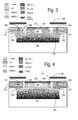
- Figure 3 shows a similar, but potentially improved (at least in terms of dark count rate) device to that of Figure 2 .
- the only difference is that the conventional p-well has been replaced with a lower-doped p-well layer, p-add 300 which, while not necessarily being conventional in the wider CMOS sense, is a layer type well known to the skilled person in CMOS imaging device processes (for example the IMG175 CMOS imaging process pioneered by the present applicant). It should be noted that use of this p-add implant will require an extra mask and fabrication step.
- This lower doped p-well implant, p-add 300 forms a progressively graded junction into the n-type region, while again the N donor region is graded back up towards the anode by using the "deep n-well" implant without a conventional n-well.
- the depletion region is correspondingly larger and dark count lower, so low in fact that it is in the region of 30 Hz, which is a couple of orders of magnitude lower than the example of Figure 2 and therefore many orders of magnitude lower than the corresponding prior art.
- other parameters are within acceptable limits, such that the device is practical in use.
- Figure 4 shows a further SPAD design.
- This design differs from having above the deep n-well implant, a breakdown region formed from both an n-well implant 250, and an implant of p-add 300, the lower doped p material used in the breakdown region of the SPAD of Figure 3 .
- the effect of this p-add implant (which is implanted after the n-well) is to create a graded breakdown region 400 (due to the progressive deep n-well 210), which therefore has a deeper and wider depletion region extending into the n-well 250. This again results in a very low dark count (approximately 30Hz).
- guard ring is partially formed the lower doped p-implant, although the outer periphery of the guard ring is formed from the deep n-well graded p-epi layer as in the other examples above.
- the guard ring has an inner region that is higher doped (though still relatively low doped) than its outer region. Therefore, again there is provided a low field guard ring, but in this case with a field that decreases from its inside to its periphery.
- One particular advantage of this arrangement is that, not only is the dark current leakage very low, but so is the breakdown voltage (-12.6v).
- This means that the deep n-well can be shared with other devices, as this breakdown voltage is less than the breakdown voltage of the deep n-well and p-substrate junction and of a p-well and deep n-well junction. Therefore one or more p-wells can also be formed in the deep n-well, without risk of the consequent p-n junction breaking down due to the -12.6v required for the SPAD to operate.
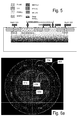
- Figure 5 shows such an integrated device (unlabelled for clarity, each implant corresponding to the appropriate implants of Figures 2 to 4 ), showing a SPAD and NMOS transistor sharing the same deep n-well and substrate.
- the SPAD is the same as depicted in Figure 4
- the NMOS transistor is conventional and its structure and operation, which will be immediately apparent to the skilled person without further description here.
- the NMOS devices are formed in p-well regions within the deep n-well. These NMOS devices may be connected in such a way as to perform quenching and readout operations on a SPAD, that is the anode of a SPAD may be connected to the drain AND/OR gate of an NMOS device or devices to perform quenching or readout.
- An array of SPADs and NMOS transistors can be formed in the same deep well, thereby forming an addressable imaging array. While the SPAD of Figure 4 is shown here, it will be appreciated that any of other SPAD according to the invention could be used, provided that its breakdown voltage is lower than that of any other p-n junctions on the device.
- Figure 6 shows the SPAD of Figure 2 from above. It can be seen that the shape of the SPAD 600, and the main implants/wells 610a, 610b, 610c, 610d are all substantially round. This is advantageous in SPAD design, in particular in reducing breakdown homogeneity, due to relatively high field areas being formed at the periphery of non-circular SPADs, particularly at the vertices of conventional octagonal designs. However, such designs break the CMOS design rules and accepted practice, insofar as CMOS design software will only sallow devices and implants of shapes with angles of either 45 or 90 degrees.
- SPAD of Figure 6 An alternative to the SPAD of Figure 6 , which also achieves many of the same advantages while maximising the active area, is a SPAD of rectangular or square design, but with rounded corners made the same way as that detailed in Figure 6b .
- CMOS implants or at least the conventional implants available for more specific CMOS technologies, for example imaging
- at least one lower doped implant than used in conventional SPADs to form one side of the p-n junction, so as to widen the depletion layer.
- all the devices have been described in relation to their formation in p-epi, but may equally be formed in n-epi, with opposite doping for all the implants, as appropriate.
Landscapes
- Solid State Image Pick-Up Elements (AREA)
- Light Receiving Elements (AREA)
- Prostheses (AREA)
Priority Applications (1)
| Application Number | Priority Date | Filing Date | Title |
|---|---|---|---|
| EP12154783.0A EP2455985A3 (de) | 2008-07-10 | 2008-07-10 | Verbesserungen von Einzelphoton-Avalanche-Dioden |
Applications Claiming Priority (2)
| Application Number | Priority Date | Filing Date | Title |
|---|---|---|---|
| EP12154783.0A EP2455985A3 (de) | 2008-07-10 | 2008-07-10 | Verbesserungen von Einzelphoton-Avalanche-Dioden |
| EP08275029A EP2144303B1 (de) | 2008-07-10 | 2008-07-10 | Verbesserungen von Einzelphoton-Lawinendioden |
Related Parent Applications (1)
| Application Number | Title | Priority Date | Filing Date |
|---|---|---|---|
| EP08275029.0 Division | 2008-07-10 |
Publications (2)
| Publication Number | Publication Date |
|---|---|
| EP2455985A2 true EP2455985A2 (de) | 2012-05-23 |
| EP2455985A3 EP2455985A3 (de) | 2013-07-17 |
Family
ID=40139269
Family Applications (3)
| Application Number | Title | Priority Date | Filing Date |
|---|---|---|---|
| EP12154782.2A Withdrawn EP2455984A3 (de) | 2008-07-10 | 2008-07-10 | Verbesserungen von Einzelphoton-Avalanche-Dioden |
| EP08275029A Not-in-force EP2144303B1 (de) | 2008-07-10 | 2008-07-10 | Verbesserungen von Einzelphoton-Lawinendioden |
| EP12154783.0A Withdrawn EP2455985A3 (de) | 2008-07-10 | 2008-07-10 | Verbesserungen von Einzelphoton-Avalanche-Dioden |
Family Applications Before (2)
| Application Number | Title | Priority Date | Filing Date |
|---|---|---|---|
| EP12154782.2A Withdrawn EP2455984A3 (de) | 2008-07-10 | 2008-07-10 | Verbesserungen von Einzelphoton-Avalanche-Dioden |
| EP08275029A Not-in-force EP2144303B1 (de) | 2008-07-10 | 2008-07-10 | Verbesserungen von Einzelphoton-Lawinendioden |
Country Status (2)
| Country | Link |
|---|---|
| US (2) | US8217436B2 (de) |
| EP (3) | EP2455984A3 (de) |
Families Citing this family (79)
| Publication number | Priority date | Publication date | Assignee | Title |
|---|---|---|---|---|
| US8324554B2 (en) | 2010-03-23 | 2012-12-04 | Massachusetts Institute Of Technology | Single-electron detection method and apparatus for solid-state intensity image sensors with a charge-metering device |
| GB201014843D0 (en) * | 2010-09-08 | 2010-10-20 | Univ Edinburgh | Single photon avalanche diode for CMOS circuits |
| WO2012048288A1 (en) * | 2010-10-07 | 2012-04-12 | Silicon Biodevices, Inc. | Magnetic particle based biosensor |
| GB2485993A (en) | 2010-11-30 | 2012-06-06 | St Microelectronics Res & Dev | Sports equipment comprising proximity detector using single photon avalanche diode (SPAD) for measuring the speed of an object struck by the sports equipment |
| GB2485991A (en) * | 2010-11-30 | 2012-06-06 | St Microelectronics Res & Dev | Camera using a Single Photon Avalanche Diode (SPAD) array |
| GB2485994A (en) | 2010-11-30 | 2012-06-06 | St Microelectronics Res & Dev | Navigation device using a Single Photon Avalanche Diode (SPAD) detector |
| GB2486165A (en) | 2010-11-30 | 2012-06-13 | St Microelectronics Res & Dev | Oven using a Single Photon Avalanche Diode (SPAD) array |
| GB2487958A (en) * | 2011-02-10 | 2012-08-15 | St Microelectronics Res & Dev | A multi-mode photodetector pixel |
| US20120313173A1 (en) * | 2011-06-07 | 2012-12-13 | Rf Micro Devices, Inc. | Method for isolating rf functional blocks on silicon-on-insulator (soi) substrates |
| EP2549536B1 (de) * | 2011-07-22 | 2020-08-19 | Espros Photonics AG | Halbleiterstruktur zur Photonendetektion |
| GB2494663A (en) | 2011-09-14 | 2013-03-20 | St Microelectronics Res & Dev | A system and corresponding method for monitoring vibration isolators |
| WO2013066959A1 (en) * | 2011-10-31 | 2013-05-10 | The Trustees Of Columbia University In The City Of New York | Systems and methods for imaging using single photon avalanche diodes |
| FR2984610A1 (fr) * | 2011-12-16 | 2013-06-21 | St Microelectronics Grenoble 2 | Montage de photodiode a avalanche pour la detection de photons uniques |
| FR2984607A1 (fr) * | 2011-12-16 | 2013-06-21 | St Microelectronics Crolles 2 | Capteur d'image a photodiode durcie |
| US9231078B2 (en) * | 2012-12-05 | 2016-01-05 | Macronix International Co., Ltd. | Semiconductor and manufacturing method thereof |
| KR101964891B1 (ko) * | 2013-01-28 | 2019-08-07 | 삼성전자주식회사 | 실리콘 광증배관 디텍터 셀 |
| US9178058B2 (en) | 2013-03-13 | 2015-11-03 | Taiwan Semiconductor Manufacturing Company, Ltd. | RF switch on high resistive substrate |
| US9917168B2 (en) | 2013-06-27 | 2018-03-13 | Taiwan Semiconductor Manufacturing Company, Ltd. | Metal oxide semiconductor field effect transistor having variable thickness gate dielectric |
| FR3009889B1 (fr) | 2013-08-23 | 2016-12-23 | Commissariat Energie Atomique | Photodiode a haut rendement quantique |
| JP6090060B2 (ja) | 2013-08-23 | 2017-03-08 | 株式会社豊田中央研究所 | シングルフォトンアバランシェダイオード |
| FR3009888B1 (fr) | 2013-08-23 | 2015-09-18 | Commissariat Energie Atomique | Photodiode spad a haut rendement quantique |
| CN103779437A (zh) * | 2014-02-17 | 2014-05-07 | 苏州超锐微电子有限公司 | 一种基于标准cmos工艺的单光子级分辨率传感器单元结构 |
| US9568620B2 (en) | 2014-09-22 | 2017-02-14 | General Electric Company | Solid state photomultiplier |
| US9383404B2 (en) * | 2014-12-05 | 2016-07-05 | Globalfoundries Inc. | High resistivity substrate final resistance test structure |
| CN105810775B (zh) * | 2014-12-31 | 2017-09-12 | 湘潭大学 | 一种基于cmos图像传感器工艺的np型单光子雪崩二极管 |
| CN104810377B (zh) * | 2015-03-04 | 2018-03-06 | 南京邮电大学 | 一种高集成度的单光子雪崩二极管探测器阵列单元 |
| US9602804B2 (en) * | 2015-03-26 | 2017-03-21 | Intel Corporation | Methods of forming integrated package structures with low Z height 3D camera |
| US9847363B2 (en) | 2015-10-20 | 2017-12-19 | Taiwan Semiconductor Manufacturing Company, Ltd. | Semiconductor device with a radiation sensing region and method for forming the same |
| US11081612B2 (en) * | 2015-12-01 | 2021-08-03 | Sharp Kabushiki Kaisha | Avalanche photodiode |
| US10014340B2 (en) | 2015-12-28 | 2018-07-03 | Taiwan Semiconductor Manufacturing Co., Ltd. | Stacked SPAD image sensor |
| CN107026212A (zh) * | 2016-01-29 | 2017-08-08 | 苏州超锐微电子有限公司 | 一种基于标准工艺的双pn结型单光子雪崩二极管结构 |
| EP3206234B1 (de) * | 2016-02-09 | 2023-08-09 | ams AG | Halbleiterelement mit einer einzelphotonen-lawinendiode und verfahren zur herstellung solch eines halbleiterelements |
| CN106057958B (zh) * | 2016-08-08 | 2017-05-10 | 杭州电子科技大学 | 单光子雪崩光电二极管的制作方法 |
| JP2020009790A (ja) * | 2016-11-09 | 2020-01-16 | シャープ株式会社 | アバランシェフォトダイオード |
| GB2557303B (en) * | 2016-12-05 | 2020-08-12 | X Fab Semiconductor Foundries Gmbh | Photodiode device and method of manufacture |
| CN106847960B (zh) * | 2017-01-23 | 2019-04-09 | 重庆邮电大学 | 一种基于深n阱结构的单光子雪崩二极管及其制作工艺 |
| US10103285B1 (en) * | 2017-04-13 | 2018-10-16 | Taiwan Semiconductor Manufacturing Company Ltd. | Semiconductor device and method of manufacturing the same |
| US10205037B2 (en) * | 2017-06-09 | 2019-02-12 | Taiwan Semiconductor Manufacturing Company Ltd. | Photodiode device and manufacturing method thereof |
| US20200144436A1 (en) * | 2017-06-26 | 2020-05-07 | Sony Semiconductor Solutions Corporation | Single-photon avalanche diode and method for operating a single-photon avalanche diode |
| EP3435422B1 (de) * | 2017-07-26 | 2020-05-06 | ams AG | Spad-vorrichtung zur überwachung von übermässiger vorspannung |
| EP3435419A1 (de) * | 2017-07-26 | 2019-01-30 | ams AG | Halbleiterbauelement mit einzelelektronenzählfunktion mit einem avalanche bipolartransistor |
| DE102018122925A1 (de) * | 2017-09-29 | 2019-04-04 | Taiwan Semiconductor Manufacturing Company, Ltd. | Spad image sensor and associated fabricating method |
| US10636930B2 (en) * | 2017-09-29 | 2020-04-28 | Taiwan Semiconductor Manufacturing Company Ltd. | SPAD image sensor and associated fabricating method |
| US10204950B1 (en) | 2017-09-29 | 2019-02-12 | Taiwan Semiconductor Manufacturing Company Ltd. | SPAD image sensor and associated fabricating method |
| US10672934B2 (en) * | 2017-10-31 | 2020-06-02 | Taiwan Semiconductor Manufacturing Company Ltd. | SPAD image sensor and associated fabricating method |
| US10410934B2 (en) * | 2017-12-07 | 2019-09-10 | Micron Technology, Inc. | Apparatuses having an interconnect extending from an upper conductive structure, through a hole in another conductive structure, and to an underlying structure |
| US10971533B2 (en) * | 2018-01-29 | 2021-04-06 | Stmicroelectronics (Crolles 2) Sas | Vertical transfer gate with charge transfer and charge storage capabilities |
| JP7129199B2 (ja) * | 2018-04-11 | 2022-09-01 | キヤノン株式会社 | 光検出装置、光検出システム及び移動体 |
| US10854658B2 (en) | 2018-07-16 | 2020-12-01 | Taiwan Semiconductor Manufacturing Company, Ltd. | Image sensor with sidewall protection and method of making same |
| US11018168B2 (en) | 2018-09-20 | 2021-05-25 | Taiwan Semiconductor Manufacturing Co., Ltd. | Image sensor with improved timing resolution and photon detection probability |
| CN110931578B (zh) * | 2018-09-20 | 2024-05-28 | 台湾积体电路制造股份有限公司 | 光电探测器及其形成方法 |
| US10896953B2 (en) * | 2019-04-12 | 2021-01-19 | Globalfoundries Inc. | Diode structures |
| CN110246903B (zh) * | 2019-06-28 | 2021-05-28 | 湖南师范大学 | 低噪声宽光谱响应的单光子雪崩光电二极管及其制作方法 |
| FR3098075A1 (fr) | 2019-06-28 | 2021-01-01 | Stmicroelectronics (Crolles 2) Sas | Pixel et son procédé de commande |
| EP4052304B1 (de) * | 2019-10-31 | 2025-06-25 | The Regents of the University of California | Avalanche-detektor mit tiefem übergang und geringer verstärkung |
| CN112909033A (zh) * | 2019-12-04 | 2021-06-04 | 半导体元件工业有限责任公司 | 半导体器件 |
| CN110993710B (zh) * | 2019-12-30 | 2021-11-02 | 上海集成电路研发中心有限公司 | 一种单光子雪崩二极管及其制备方法 |
| US11646335B2 (en) * | 2020-01-30 | 2023-05-09 | Semiconductor Components Industries, Llc | Semiconductor devices with single-photon avalanche diodes and rectangular microlenses |
| CN115461868B (zh) * | 2020-03-20 | 2025-06-20 | 灵明光子有限公司 | 用于直接飞行时间传感器的spad像素电路及其方法 |
| US11522097B2 (en) * | 2020-10-14 | 2022-12-06 | Globalfoundries Singapore Pte. Ltd. | Diode devices and methods of forming diode devices |
| CN112490300B (zh) * | 2020-10-29 | 2022-07-22 | 西安电子科技大学 | 一种共用深n阱的spad器件及其构成的光探测阵列 |
| KR102883860B1 (ko) * | 2021-02-09 | 2025-11-07 | 에스케이하이닉스 주식회사 | 단일 광자 애벌런치 다이오드 |
| CN216698365U (zh) * | 2021-02-26 | 2022-06-07 | 神盾股份有限公司 | 单光子雪崩二极管及单光子雪崩二极管阵列 |
| CN113284971B (zh) * | 2021-04-14 | 2025-07-25 | 中国计量大学 | 一种背面照射的单光子雪崩二极管及其制作方法 |
| US12402426B2 (en) * | 2021-08-31 | 2025-08-26 | Trupixel Inc. | Single-photon detection device, single-photon detector, and single-photon detector array |
| CN113690337B (zh) * | 2021-09-13 | 2023-12-08 | 武汉新芯集成电路制造有限公司 | 单光子雪崩二极管及其制作方法、单光子雪崩二极管阵列 |
| US20250015083A1 (en) * | 2021-11-01 | 2025-01-09 | Wesley Harold Morris | Shallow Buried Guard Ring (SBGR) Isolation Structures and Fabrication Models to Enable Latchup Immunity in CMOS Integrated Circuits Operating in Extreme Radiation Environments and Temperatures Ranges |
| CN114122186B (zh) * | 2021-11-29 | 2024-05-14 | 中国电子科技集团公司第四十四研究所 | 一种像元边缘低电场强度的硅光电倍增管及其制造方法 |
| CN114551631B (zh) * | 2022-01-25 | 2025-04-22 | 西安电子科技大学 | 一种背照式硅基单光子雪崩二极管结构及光电探测器 |
| CN114354729B (zh) * | 2022-03-18 | 2022-06-21 | 南昌大学 | 毛细管电泳检测装置 |
| US11967664B2 (en) * | 2022-04-20 | 2024-04-23 | Globalfoundries Singapore Pte. Ltd. | Photodiodes with serpentine shaped electrical junction |
| TWI882322B (zh) * | 2022-05-06 | 2025-05-01 | 奧地利商Ams歐斯朗股份公司 | 單光子崩潰二極體、單光子崩潰二極體陣列、單光子崩潰二極體像素讀出式電路及單光子崩潰二極體之製造方法 |
| KR102711235B1 (ko) | 2022-06-24 | 2024-09-27 | 주식회사 트루픽셀 | 단일 광자 검출 소자, 전자 장치, 및 라이다 장치 |
| CN115425101B (zh) * | 2022-09-19 | 2024-04-16 | 南京邮电大学 | 一种双结单光子雪崩二极管、探测器及制作方法 |
| KR102678796B1 (ko) | 2023-01-13 | 2024-06-26 | 주식회사 트루픽셀 | 단일 광자 검출기, 전자 장치, 및 라이다 장치 |
| KR102735202B1 (ko) * | 2023-02-13 | 2024-11-28 | 주식회사 솔리드뷰 | 수광센서를 위한 afe 소자 및 그 제어방법 |
| CN117239000B (zh) * | 2023-11-10 | 2024-03-19 | 北京中科海芯科技有限公司 | 一种雪崩光电二极管及其制作方法、单光子探测器 |
| CN117936621B (zh) * | 2023-12-30 | 2026-03-06 | 阜时科技有限公司 | 光电转换器件及其制备方法、光电检测装置、电子设备 |
| CN119364915B (zh) * | 2024-12-12 | 2025-03-18 | 成都中微达信科技有限公司 | 光电二极管、二极管组件及光滤波器 |
Family Cites Families (9)
| Publication number | Priority date | Publication date | Assignee | Title |
|---|---|---|---|---|
| AU2185499A (en) * | 1998-01-30 | 1999-08-16 | Hamamatsu Photonics K.K. | Light-receiving semiconductor device with buit-in bicmos and avalanche photodiode |
| GB2367945B (en) * | 2000-08-16 | 2004-10-20 | Secr Defence | Photodetector circuit |
| AU2002238699A1 (en) * | 2002-02-08 | 2003-09-02 | Qinetiq Limited | Photodetector circuit |
| US7166878B2 (en) * | 2003-11-04 | 2007-01-23 | Sarnoff Corporation | Image sensor with deep well region and method of fabricating the image sensor |
| US7262402B2 (en) * | 2005-02-14 | 2007-08-28 | Ecole Polytechnique Federal De Lausanne | Integrated imager circuit comprising a monolithic array of single photon avalanche diodes |
| JP4817746B2 (ja) * | 2005-07-27 | 2011-11-16 | 株式会社東芝 | 半導体装置の設計データ処理方法、そのプログラム、及び半導体装置の製造方法 |
| JP5437791B2 (ja) * | 2006-04-25 | 2014-03-12 | コーニンクレッカ フィリップス エヌ ヴェ | (Bi)CMOSプロセスによるアバランシェフォトダイオードの製造方法 |
| US8188563B2 (en) * | 2006-07-21 | 2012-05-29 | The Regents Of The University Of California | Shallow-trench-isolation (STI)-bounded single-photon CMOS photodetector |
| WO2008113067A2 (en) * | 2007-03-15 | 2008-09-18 | Johns Hopkins University | Deep submicron and nano cmos single photon photodetector pixel with event based circuits for readout data-rate reduction |
-
2008
- 2008-07-10 EP EP12154782.2A patent/EP2455984A3/de not_active Withdrawn
- 2008-07-10 EP EP08275029A patent/EP2144303B1/de not_active Not-in-force
- 2008-07-10 EP EP12154783.0A patent/EP2455985A3/de not_active Withdrawn
-
2009
- 2009-07-07 US US12/498,874 patent/US8217436B2/en active Active
-
2012
- 2012-04-24 US US13/454,811 patent/US8552482B2/en active Active
Non-Patent Citations (1)
| Title |
|---|
| None |
Also Published As
| Publication number | Publication date |
|---|---|
| US20100019295A1 (en) | 2010-01-28 |
| EP2144303B1 (de) | 2013-02-06 |
| US20120205731A1 (en) | 2012-08-16 |
| US8217436B2 (en) | 2012-07-10 |
| EP2455984A3 (de) | 2013-07-17 |
| EP2455985A3 (de) | 2013-07-17 |
| EP2455984A2 (de) | 2012-05-23 |
| US8552482B2 (en) | 2013-10-08 |
| EP2144303A1 (de) | 2010-01-13 |
Similar Documents
| Publication | Publication Date | Title |
|---|---|---|
| EP2144303B1 (de) | Verbesserungen von Einzelphoton-Lawinendioden | |
| EP2150991B1 (de) | Methode zur ausbildung einer lawinen-fotodiode integriert mit cmos-schaltkreisen und mit dieser methode hergestellter silizium-fotovervielfacher | |
| EP3206234B1 (de) | Halbleiterelement mit einer einzelphotonen-lawinendiode und verfahren zur herstellung solch eines halbleiterelements | |
| US10847668B2 (en) | Avalanche photodiode | |
| US9178100B2 (en) | Single photon avalanche diode for CMOS circuits | |
| US8779543B2 (en) | Device having an avalanche photo diode and a method for sensing photons | |
| EP1839343B1 (de) | Halbleiterphotodiode und herstellungsverfahren dafür | |
| JP2015041746A (ja) | シングルフォトンアバランシェダイオード | |
| CN114207846B (zh) | 雪崩光电二极管和用于制造雪崩光电二极管的方法 | |
| TWI647858B (zh) | 具有降低暗計數率之單光子雪崩光電二極體探測器的裝置和方法 | |
| Kamrani et al. | Premature edge breakdown prevention techniques in CMOS APD fabrication | |
| EP3809472B1 (de) | Ein-photonen-lawinendiode und sensoranordnung | |
| CN111628033A (zh) | 光电探测装置的制造方法 | |
| CN119545927A (zh) | 雪崩二极管和探测器 | |
| CN114551631B (zh) | 一种背照式硅基单光子雪崩二极管结构及光电探测器 | |
| KR101091205B1 (ko) | 암전류가 감소된 실리콘 광전자 증배관 | |
| CN113224197B (zh) | 一种雪崩探测器及制备方法 | |
| JP7199013B2 (ja) | 光検出器 | |
| Zhou et al. | Effect of deep virtual guard ring on performance of a miniaturized high-photo-sensitivity silicon single-photon avalanche diode | |
| CN117790613A (zh) | 单光子雪崩二极管、电子设备及激光雷达设备 | |
| CN121909759A (zh) | 在BCD制程中产生埋置p-n接面的方法、BCD衬底和以此为基础的单光子雪崩二极管 | |
| CN121924850A (zh) | 具有sti结构的单光子雪崩二极管 |
Legal Events
| Date | Code | Title | Description |
|---|---|---|---|
| PUAI | Public reference made under article 153(3) epc to a published international application that has entered the european phase |
Free format text: ORIGINAL CODE: 0009012 |
|
| AC | Divisional application: reference to earlier application |
Ref document number: 2144303 Country of ref document: EP Kind code of ref document: P |
|
| AK | Designated contracting states |
Kind code of ref document: A2 Designated state(s): AT BE BG CH CY CZ DE DK EE ES FI FR GB GR HR HU IE IS IT LI LT LU LV MC MT NL NO PL PT RO SE SI SK TR |
|
| PUAL | Search report despatched |
Free format text: ORIGINAL CODE: 0009013 |
|
| AK | Designated contracting states |
Kind code of ref document: A3 Designated state(s): AT BE BG CH CY CZ DE DK EE ES FI FR GB GR HR HU IE IS IT LI LT LU LV MC MT NL NO PL PT RO SE SI SK TR |
|
| RIC1 | Information provided on ipc code assigned before grant |
Ipc: H01L 31/107 20060101AFI20130607BHEP |
|
| STAA | Information on the status of an ep patent application or granted ep patent |
Free format text: STATUS: THE APPLICATION IS DEEMED TO BE WITHDRAWN |
|
| 18D | Application deemed to be withdrawn |
Effective date: 20140118 |