EP4052304B1 - Avalanche-detektor mit tiefem übergang und geringer verstärkung - Google Patents
Avalanche-detektor mit tiefem übergang und geringer verstärkung Download PDFInfo
- Publication number
- EP4052304B1 EP4052304B1 EP20881342.8A EP20881342A EP4052304B1 EP 4052304 B1 EP4052304 B1 EP 4052304B1 EP 20881342 A EP20881342 A EP 20881342A EP 4052304 B1 EP4052304 B1 EP 4052304B1
- Authority
- EP
- European Patent Office
- Prior art keywords
- type
- region
- lgad
- gain
- dopant density
- Prior art date
- Legal status (The legal status is an assumption and is not a legal conclusion. Google has not performed a legal analysis and makes no representation as to the accuracy of the status listed.)
- Active
Links
Images




Classifications
-
- H—ELECTRICITY
- H10—SEMICONDUCTOR DEVICES; ELECTRIC SOLID-STATE DEVICES NOT OTHERWISE PROVIDED FOR
- H10F—INORGANIC SEMICONDUCTOR DEVICES SENSITIVE TO INFRARED RADIATION, LIGHT, ELECTROMAGNETIC RADIATION OF SHORTER WAVELENGTH OR CORPUSCULAR RADIATION
- H10F30/00—Individual radiation-sensitive semiconductor devices in which radiation controls the flow of current through the devices, e.g. photodetectors
- H10F30/20—Individual radiation-sensitive semiconductor devices in which radiation controls the flow of current through the devices, e.g. photodetectors the devices having potential barriers, e.g. phototransistors
- H10F30/21—Individual radiation-sensitive semiconductor devices in which radiation controls the flow of current through the devices, e.g. photodetectors the devices having potential barriers, e.g. phototransistors the devices being sensitive to infrared, visible or ultraviolet radiation
- H10F30/22—Individual radiation-sensitive semiconductor devices in which radiation controls the flow of current through the devices, e.g. photodetectors the devices having potential barriers, e.g. phototransistors the devices being sensitive to infrared, visible or ultraviolet radiation the devices having only one potential barrier, e.g. photodiodes
- H10F30/225—Individual radiation-sensitive semiconductor devices in which radiation controls the flow of current through the devices, e.g. photodetectors the devices having potential barriers, e.g. phototransistors the devices being sensitive to infrared, visible or ultraviolet radiation the devices having only one potential barrier, e.g. photodiodes the potential barrier working in avalanche mode, e.g. avalanche photodiodes
-
- H—ELECTRICITY
- H10—SEMICONDUCTOR DEVICES; ELECTRIC SOLID-STATE DEVICES NOT OTHERWISE PROVIDED FOR
- H10F—INORGANIC SEMICONDUCTOR DEVICES SENSITIVE TO INFRARED RADIATION, LIGHT, ELECTROMAGNETIC RADIATION OF SHORTER WAVELENGTH OR CORPUSCULAR RADIATION
- H10F77/00—Constructional details of devices covered by this subclass
- H10F77/10—Semiconductor bodies
- H10F77/14—Shape of semiconductor bodies; Shapes, relative sizes or dispositions of semiconductor regions within semiconductor bodies
-
- H—ELECTRICITY
- H10—SEMICONDUCTOR DEVICES; ELECTRIC SOLID-STATE DEVICES NOT OTHERWISE PROVIDED FOR
- H10F—INORGANIC SEMICONDUCTOR DEVICES SENSITIVE TO INFRARED RADIATION, LIGHT, ELECTROMAGNETIC RADIATION OF SHORTER WAVELENGTH OR CORPUSCULAR RADIATION
- H10F30/00—Individual radiation-sensitive semiconductor devices in which radiation controls the flow of current through the devices, e.g. photodetectors
- H10F30/20—Individual radiation-sensitive semiconductor devices in which radiation controls the flow of current through the devices, e.g. photodetectors the devices having potential barriers, e.g. phototransistors
- H10F30/29—Individual radiation-sensitive semiconductor devices in which radiation controls the flow of current through the devices, e.g. photodetectors the devices having potential barriers, e.g. phototransistors the devices being sensitive to radiation having very short wavelengths, e.g. X-rays, gamma-rays or corpuscular radiation
-
- H—ELECTRICITY
- H10—SEMICONDUCTOR DEVICES; ELECTRIC SOLID-STATE DEVICES NOT OTHERWISE PROVIDED FOR
- H10F—INORGANIC SEMICONDUCTOR DEVICES SENSITIVE TO INFRARED RADIATION, LIGHT, ELECTROMAGNETIC RADIATION OF SHORTER WAVELENGTH OR CORPUSCULAR RADIATION
- H10F39/00—Integrated devices, or assemblies of multiple devices, comprising at least one element covered by group H10F30/00, e.g. radiation detectors comprising photodiode arrays
- H10F39/10—Integrated devices
- H10F39/103—Integrated devices the at least one element covered by H10F30/00 having potential barriers, e.g. integrated devices comprising photodiodes or phototransistors
-
- H—ELECTRICITY
- H10—SEMICONDUCTOR DEVICES; ELECTRIC SOLID-STATE DEVICES NOT OTHERWISE PROVIDED FOR
- H10F—INORGANIC SEMICONDUCTOR DEVICES SENSITIVE TO INFRARED RADIATION, LIGHT, ELECTROMAGNETIC RADIATION OF SHORTER WAVELENGTH OR CORPUSCULAR RADIATION
- H10F71/00—Manufacture or treatment of devices covered by this subclass
- H10F71/121—The active layers comprising only Group IV materials
-
- H—ELECTRICITY
- H10—SEMICONDUCTOR DEVICES; ELECTRIC SOLID-STATE DEVICES NOT OTHERWISE PROVIDED FOR
- H10F—INORGANIC SEMICONDUCTOR DEVICES SENSITIVE TO INFRARED RADIATION, LIGHT, ELECTROMAGNETIC RADIATION OF SHORTER WAVELENGTH OR CORPUSCULAR RADIATION
- H10F77/00—Constructional details of devices covered by this subclass
- H10F77/10—Semiconductor bodies
- H10F77/12—Active materials
- H10F77/122—Active materials comprising only Group IV materials
- H10F77/1223—Active materials comprising only Group IV materials characterised by the dopants
Definitions
- the present invention relates to low gain avalanche detectors (LGAD) and methods of making the same.
- Avalanche diodes are used as photon detectors in many applications.
- the detection process comprises (1) the avalanche diode generating electrons and holes in response to electromagnetic radiation, charged particles, or photons; (2) separating the electrons and holes in the diode using a strong reverse bias voltage applied to the diode; (3) using the strong reverse bias voltage to further accelerate the electrons in the diode and generate additional electrons through impact ionization (an internal gain mechanism); and (4) forming a detection signal using the multiple electrons generated through the impact ionization from each of the photo-generated electrons.
- Figure 1 illustrates a Low-Gain-Avalanche-Detector (LGAD) having an n + -type layer (cathode) forming a junction with a p-type multiplication layer. Electrons are photo-generated in a p-type bulk region in response to the electromagnetic radiation and the p - type multiplication layer is the gain layer wherein the additional electrons are generated through the impact ionization.
- a p + -anode is formed on the p-type bulk region so that an ohmic connection can be made between the p-type bulk and an anode plane that allows for the application of a reverse bias voltage across the anode and the cathode.
- Such an LGAD fabricated in silicon can be used for particle detection, particularly in the arena of ultra-fast ( ⁇ 10 ps) timing.
- the high electric fields needed to induce the impact ionization process lead to breakdown between the separated n-p junctions that are used to simultaneously deplete the sensors and establish the readout segmentation.
- working devices have included a Junction Termination Extension (JTE) that provides electrostatic isolation between neighboring implants, but at a cost of introducing a dead region between the sensor segments that is insensitive to the deposited charge from an incident charged particle or photon.
- the width of this dead region is 50 ⁇ m or more, making conventional LGAD sensors inefficient for granularity or spatial resolution scales much below 1mm.
- avalanche diodes use high electric fields to provide signal gain by using a high electric field at or near a p-n junction to generate an "avalanche" of additional signal charge.
- the high electric field can also cause breakdown in the readout structure of the avalanche diode, resulting in a limit to the granularity of the readout from the diode.
- LGAD Low-Gain Avalanche Detector
- a planar, highly-doped diode junction is buried several micrometers below the surface of the device, allowing for a low electric field region in the area close to the surface readout structure while the high electric field region in the area of the junction produces the gain characteristic of LGADs.
- the buried diode junction eliminates the need for the Junction-Termination Extension (JTE) structure, employed in conventional LGADs, that limits achievable granularity.
- JTE Junction-Termination Extension
- the significantly higher degree of granularity achievable using embodiments described herein opens up a range of additional applications for the LGAD.
- the present disclosure describes an entirely novel approach to the problem of improving the granularity of LGAD sensors - the Deep Junction (“DJ-LGAD”) LGAD comprising the high electric-field gain region (wherein impact ionization takes place) moved away from the readout structure.
- DJ-LGAD Deep Junction
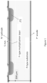
- Figure 2 illustrates the LGAD comprises a diode (p-n) junction buried a few micrometers below and away from the upper surface of the LGAD (the upper surface comprising the surface where segmentation is imposed). In the example shown, such positioning of the high electric-field gain region avoids the need for the JTE.
- p-n diode
- Figure 2 illustrates an example avalanche diode 200 including a semiconductor structure 202 including an n-type region 204; a p-type region 206; and a gain region 208 buried between the n-type region 204 and the p-type region 206.
- the gain region includes an n + -type region 212 having a higher n-type dopant density than the n-type region; a p + -type region 214 having a higher p-type dopant density than the p-type region; and a p-n junction 210 including an interface 210a between the n + -type region and the p + -type region.
- the n-type region 204 includes a plurality of segments 218, each of the segments including a first surface 216 of the n-type region 204 and the semiconductor structure.
- Figure 2 further illustrates the avalanche diode as including a readout structure 222 comprising a plurality of first electrodes 224, wherein at least one of the first electrodes is on each of the segments and the first electrodes on different segments are electrically isolated from one another.
- a second electrode 226 is deposited on a second surface 228 of the semiconductor structure/p-type region and an ohmic contact 230 is formed between the p-type region and the second electrode.
- the p-n junction is reverse biased by application of an electric field between the first electrodes in the readout structure and the second electrode.
- each of the segments include implanted regions 232 having a higher dopant density than the n-type region 204.
- the implanted regions 232 form an ohmic contact with the first electrodes.
- electrostatic isolation barriers 234 e.g., p-type wells
- Figure 2 illustrates the LGAD as comprising a gain layer including both the n + region (dark blue section) and the p + region (dark red section), rather than just a dark red section.
- the gain layer comprises the full p-n junction, rather than just the p + doped area.
- a key benefit of burying the entire junction, rather than just the highly-doped p + region, is that application of a reverse bias (creating a depletion zone) establishes an electric field in the region of the junction that is similar to that of a parallel-plate capacitor.
- Table 1 illustrates a sample doping profile ("Baseline-1" configuration) that achieves these conditions (1) and (2), while maintaining electric fields at the readout surface low enough to allow for conventional segmentation techniques and avoid the use of a JTE. All further results presented herein are for the simulated behavior of this Baseline-1 configuration.
- Table 1 Doping profile parameters for the Baseline-1 version of the DJ-LGAD. The dopant densities or levels expressed herein in scientific notation MeN per centimeter cube (cm 3 ), where m is a real number and n is an integer, are equivalent to standard notation m x 10 n .
- Figure 3 shows the resulting two-dimensional electric field profile, as a function of depth into the Baseline-1 detector and of a lateral coordinate parallel to the surface of the device, for a bias voltage of 210V.
- bias voltages above 100 Volts, the electric field in the p-type drift region and the n-type isolation region is relatively insensitive to the applied voltage, leading to stable charge collection properties.
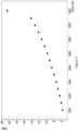
- the impact ionization process which depends upon electric field in the gain region, is also well controlled, leading to the smooth dependence of gain upon bias voltage shown in Figure 4 .
- Figure 5 shows the gain variation as a function of lateral position that results from the electric field depicted in Figure 3 ; uniformity at the +/-4% level is observed.
- Gain is defined by the collected charge in the LGAD over the collected charge in a same thickness silicon sensor without the gain layer structure.
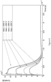
- Figure 6 shows the temporal signal profile as a function of applied bias voltage (obtained using the simulation).
- a sharp rising edge conducive to a fast timing measurement, is observed for all bias voltages, with a slew-rate that grows monotonically with bias voltage.
- Figure 7 is a flowchart illustrating a method of making an avalanche diode (referring also to Figure 2 ).
- Block 700 represents obtaining or creating a semiconductor structure (e.g., epitaxial layers) on a substrate.
- the semiconductor structure is a silicon semiconductor structure and the substrate is a silicon substrate (or the semiconductor structure and the substrate may comprise or consist essentially of silicon).
- the semiconductor structure includes a bulk p-type region; a gain region including a p-n junction on or above the bulk p-type region; and an n-type region (isolation region) on or above the gain region (n-side up configuration).
- the semiconductor structure includes a bulk n-type region; a gain region including a p-n junction on or above the bulk n-type region; and the p-type region (isolation region) on or above the gain region (p-side up configuration).
- the gain region includes an n + -type region having a higher n-type dopant density than the n-type region; a p + -type region having a higher p-type dopant density than the p-type region; and the p-n junction between the n + -type region and the p + -type region.
- the p + -type region typically forms a j unction interface in physical contact with the n + -type region.
- Example p-type dopants include, but are not limited to, boron, gallium, aluminum, and indium.
- Example n-type dopants include, but are not limited to, phosphorus, arsenic, antimony, bismuth and lithium.
- Block 702 represents forming a readout structure so that the surface of the n-type (p-type) region forms the readout structure.
- the step comprises defining a plurality of segments in the n-type region or the p-type region depending on the configuration (n-side up or p-side up).
- Block 704 represents creating or generating (e.g., depositing) a plurality of first electrodes forming an ohmic contact with the readout structure and a second electrode forming an ohmic contact with the p-type (n-type) region. At least one of the first electrodes is on each of the segments and the first electrodes on different segments are electrically isolated from one another. Established segmentation schemes for conventional (non-LGAD) silicon diode sensors may also be used.
- the step further comprises forming a first ohmic contact between the implanted regions and the first electrodes, and a second ohmic contact between the bulk p-type region and the bulk n-type region and a second electrode, so that the p-n junction is reverse biased by application of an electric field of appropriate polarity between the first electrodes and the second electrode.
- the second ohmic contact is typically formed on a second surface of the semiconductor structure opposite the first surface.
- Block 706 represents the end result, an avalanche diode.
- the avalanche diode can be used in many applications, including but not limited to, as a pixel sensor (e.g., at the large hadron collider (LHC) or proposed Electron-Ion Collider (EIC)) with fast timing capabilities.
- LHC large hadron collider
- EIC Electron-Ion Collider
- LGADs are biased with high electric fields required to induce the impact ionization process, leading to breakdown between the separated n-p junctions that are used to simultaneously deplete the sensors and establish the readout segmentation.
- working LGAD devices have included a Junction Termination Extension (JTE) that provides electrostatic isolation between neighboring implants, but at the cost of introducing a dead region between the sensor segments that is insensitive to the deposited charge from an incident particle.
- JTE Junction Termination Extension
- the width of this dead region is 50 ⁇ m or more, making conventional LGAD sensors inefficient for granularity scales much below 1mm.
- the following devices have been proposed to circumvent the JTE limit.
Landscapes
- Light Receiving Elements (AREA)
- Electrodes Of Semiconductors (AREA)
Claims (15)
- Avalanchedetektor mit geringer Verstärkung (Low Gain Avalanche Detector, LGAD) (200), umfassendeine Halbleiterstruktur (202), umfassend:einen n-Typ- (bzw. p-Typ-) Bereich (204a), der eine Vielzahl von Segmenten (218) umfasst, die jeweils einen implantierten Bereich (232) mit einer höheren Dotierungsdichte als der n-Typ- (bzw. p-Typ-) Bereich aufweisen;einen p-Typ (bzw. n-Typ) Bereich (206a); undeinen Verstärkungsbereich (208) zwischen dem n-Typ- (bzw. p-Typ-) Bereich (204a) und dem p-Typ- (bzw. n-Typ-) Bereich (206a), wobei der Verstärkungsbereich zwischen dem n-Typ- (bzw. p-Typ-) Bereich und dem p-Typ-(bzw. n-Typ-) Bereich angeordnet ist und der Verstärkungsbereich Folgendes umfasst:einen n+ -Typ Bereich (212) mit einer höheren n-Typ-Dotierstoffdichte als der n-Typ-Bereich;einen p+ -Typ Bereich (214) mit einer höheren p-Typ-Dotierstoffdichte als der p-Typ-Bereich; undeinen p-n-Übergang (210) zwischen dem n+ -Typ Bereich (212) und dem p+ -Typ Bereich (214)eine Auslesestruktur (222), umfassend
eine Vielzahl von ersten Elektroden (224), wobei:jede der ersten Elektroden sich auf einem anderen der Segmente (218) befindet,die ersten Elektroden (224) elektrisch voneinander isoliert sind; undjedes der Segmente (218) einen ersten ohmschen Kontakt zwischen dem implantierten Bereich (232) und der einen der ersten Elektroden (224) auf dem implantierten Bereich (232) umfasst;einen zweiten ohmschen Kontakt (230) zwischen dem p-Typ (bzw. n-Typ) Bereich (206a) und einer zweiten Elektrode (226) umfasst; undwobei der p-n-Übergang (210) einem elektrischen Sperrfeld ausgesetzt ist, wenn eine geeignete Polarisationsspannung zwischen den ersten Elektroden (224) und der zweiten Elektrode angelegt wird. - LGAD nach Anspruch 1, wobei die Halbleiterstruktur (202) im Wesentlichen aus Silizium besteht.
- LGAD nach Anspruch 1 oder Anspruch 2, ferner umfassend:eine erste Oberfläche (216) des n-Typ (bzw. p-Typ) Bereichs (204a);den p-n-Übergang (210), umfassend eine erste Grenzfläche (210a) zwischen dem n+ -Ttyp Bereich (212) und dem p+ -Typ Bereich (214);einen ersten Abstand D1 zwischen der ersten Grenzfläche (210a) und der ersten Oberfläche (216), der in einem Bereich von 2-10 Mikrometern liegt;eine zweite Oberfläche (228) des p-Typ- (bzw. n-Typ-) Bereichs (206a) auf einer Seite der Halbleiterstruktur gegenüber der ersten Oberfläche (216); undeinen zweiten Abstand (D2) zwischen der zweiten Oberfläche (228) und der ersten Schnittstelle (210a) in einem Bereich von 20 Mikrometern bis 100 Mikrometern.
- LGAD nach Anspruch 3, wobei der erste Abstand in einem Bereich von 3-6 Mikrometern liegt.
- LGAD nach einem der Ansprüche 1-4, wobei:der n+ -Typ Bereich (212) eine erste n-Typ-Dotierstoffdichte und der p+ -Typ Bereich (214) eine erste p-Typ-Dotierstoffdichte aufweist, unddie erste n-Typ-Dotierstoffdichte innerhalb von 10 % der ersten p-Typ-Dotierstoffdichte liegt.
- LGAD nach Anspruch 5, wobeidie erste n-Typ-Dotierstoffdichte und die erste p-Typ-Dotierstoffdichte in einem Bereich von 2,6e^16 - 3,8e^16 Dotierstoffatomen pro cm3 liegen,der n-Typ-Bereich (204a) eine zweite n-Typ-Dotierstoffdichte in einem Bereich von 1e^12 - 1e^14 Atomen pro cm3 aufweist, undder p-Typ-Bereich (206a) eine zweite p-Typ-Dotierstoffdichte in einem Bereich von 1e^12 - 1e^14 Atomen pro cm3 aufweist.
- LGAD nach einem der Ansprüche 1-6, wobei:wenn der LGAD 200 eine Verarmung erfährt, das elektrische Sperrfeld, eine erste n-Typ-Dotierstoffdichte in dem n+ -Typ-Bereich (212) und eine zweite p-Typ-Dotierstoffdichte in dem p+ -Typ-Bereich (214) in einem Bereich liegen, der eine Verstärkung unter Verwendung von Stoßionisation in dem p-n-Übergang (210) ohne Durchbruch des p-n-Übergangs (210) erreicht; undeine zweite n-Typ-Dotierstoffdichte in dem n-Typ-Bereich (204a) und eine zweite p-Typ-Dotierstoffdichte in dem p-Typ-Bereich (206a) in einem solchen Bereich liegen, dass:das elektrische Sperrfeld keine Stoßionisation im n-Typ-Bereich oder im p-Typ-Bereich auslöst,die zweite p-Typ-Dotierstoffdichte eine Sättigung der Driftgeschwindigkeit im p-Typ-Bereich ermöglicht, unddie zweite n-Typ-Dotierstoffdichte eine Sättigung der Driftgeschwindigkeit im n-Typ-Bereich ermöglicht.
- LGAD nach einem der Ansprüche 1-7, wobei:ausgehend von einer vollständigen Verarmung und als Funktion einer zunehmenden elektrischen Sperrspannung über die ersten Elektroden (224) und die zweite Elektrode (226) eine Verstärkung des LGAD monoton bis zum Durchbruch im p-n-Übergang (210) zunimmt; unddie Verstärkung gekennzeichnet ist als das Ansprechverhalten des LGAD mit dem p-n-Übergang (210) geteilt durch das Ansprechverhalten des LGAD, bei dem:der p+ -Typ Bereich (214) durch eine Fortsetzung des p-Typ-Bereichs (206a) mit derselben Dicke wie der p+ -Typ Bereich ersetzt wird, undder n+ -Typ Bereich (212) durch eine Fortsetzung des n-Typ-Bereichs (204a) mit derselben Dicke wie der n+ -Typ Bereich ersetzt wird.
- LGAD nach einem der Ansprüche 1-8, wobei:jedes der Segmente (218) eine Oberfläche von 3 mal 3 Mikrometern oder mehr hat, oderdie Zahlendichte der Segmente (218) bis zu 105 Segmente pro Quadratmillimeter beträgt.
- LGAD nach einem der Ansprüche 1-9, ferner umfassend:
eine elektrostatische Isolationsbarriere (234), die Dotierstoffe vom p-Typ ( bzw. ) vom n-Typ umfasst, zwischen benachbarten Segmenten (218), wobei:die elektrostatischen Isolationsbarrieren (234) die ersten Elektroden (218) elektrisch voneinander isolieren, unddie elektrostatischen Isolationsbarrieren (234) bis zu einer Tiefe reichen, die den p-n-Übergang (210) nicht erreicht. - LGAD nach Anspruch 10, wobei die Barrieren (234) eine dritte p-Typ- (bzw. n-Typ-) Dotierungsdichte in einem Bereich von 1e^12 - 1e^14 Dotierungsatomen pro cm3 umfassen.
- LGAD nach Anspruch 6 oder 10, wobeidie Dotierstoffdichten in der Halbleiterstruktur (202) so abgestimmt sind, dass die Verstärkung des LGAD als Funktion der Position entlang einer Länge (L) des Segments (218) in einer beliebigen Richtung parallel zur ersten Oberfläche (216) um nicht mehr als +/-10% variiert, undfür den p-Typ- (bzw. n-Typ-) Bereich (206a), der einen Bulk-Bereich mit einer Dicke von 50 Mikrometern oder weniger umfasst, der Großteil einer Signalladung als Reaktion auf das Auftreffen geladener Teilchen oder Photonen auf das LGAD innerhalb von 500 Pikosekunden auf den ersten Elektroden (224) gesammelt wird, was eine Wiederholungsrate von über 1 GHz ermöglicht.
- LGAD nach einem der Ansprüche 1-12, wobei
die implantierten Bereiche (232) eine vierte n-Typ- (bzw. p-Typ-) Dotierstoffdichte in einem Bereich von 1e^17 - 1e^19 Dotierstoffatomen pro cm3 umfassen. - LGAD nach einem der Ansprüche 1-13, wobei:die Avalanche-Diode keine Junction-Termination-Extension-Struktur (JTE-Struktur) zwischen den Segmenten (218) aufweist, undder p-Typ- (bzw. n-Typ-) Bereich (206a) einen p-Typ-Bulkbereich (bzw. n-Typ-Bulkbereich) umfasst, so dass der zweite ohmsche Kontakt (230) zwischen dem p-Typ- (bzw. n-Typ-) Bulkbereich (206) und der zweiten Elektrode (226) liegt.
- Verfahren zur Herstellung eines Avalanchedetektors mit geringer Verstärkung (Low Gain Avalanche Detectors, LGADs), umfassend:Erhalten oder Erzeugen einer Halbleiterstruktur, umfassend:einen n-Typ (bzw. p-Typ) Bereich (204a);einen p-Typ (bzw. n-Typ) Bereich (206a); undeinen Verstärkungsbereich (208) zwischen dem n-Typ-Bereich und dem p-Typ-Bereich, wobei der Verstärkungsbereich zwischen dem n-Typ-Bereich und dem p-Typ-Bereich angeordnet ist und der Verstärkungsbereich umfasst:einen n+ -Typ Bereich (212) mit einer höheren n-Typ-Dotierstoffdichte als der n-Typ-Bereich;einen p+ -Typ Bereich (214) mit einer höheren p-Typ-Dotierstoffdichte als der p-Typ-Bereich; undeinen p-n-Übergang (210) zwischen dem n+ -Typ Bereich und dem p+ -Typ Bereichdie Oberfläche des n-Typ- (bzw. p-Typ-) Bereichs, eine Auslesestruktur (222) bildend, umfassend:
eine Vielzahl von Segmenten (218) in dem n-Typ- (bzw. p-Typ-) Bereich, wobei jedes der Segmente einen implantierten Bereich (232) umfasst, der eine höhere Dotierungsdichte als der n-Typ- (bzw. p-Typ-) Bereich aufweistErzeugen einer Vielzahl von ersten Elektroden (224), wobei sich jede der ersten Elektroden auf einem anderen der Segmente befindet und die ersten Elektroden elektrisch voneinander isoliert sindBilden eines ersten ohmschen Kontakts zwischen jedem der implantierten Bereiche und der einen der ersten Elektroden auf jedem der implantierten Bereiche; undBilden eines zweiten ohmschen Kontakts zwischen dem p-Typ (bzw. n-Typ) Bereich und einer zweiten Elektrode (226), so dass der p-n-Übergang (210) durch Anlegen eines elektrischen Feldes geeigneter Polarität zwischen den ersten Elektroden und der zweiten Elektrode in Sperrichtung vorgespannt wird.
Applications Claiming Priority (2)
| Application Number | Priority Date | Filing Date | Title |
|---|---|---|---|
| US201962928775P | 2019-10-31 | 2019-10-31 | |
| PCT/US2020/058176 WO2021087237A1 (en) | 2019-10-31 | 2020-10-30 | Deep junction low-gain avalanche detector |
Publications (3)
| Publication Number | Publication Date |
|---|---|
| EP4052304A1 EP4052304A1 (de) | 2022-09-07 |
| EP4052304A4 EP4052304A4 (de) | 2022-12-28 |
| EP4052304B1 true EP4052304B1 (de) | 2025-06-25 |
Family
ID=75716469
Family Applications (1)
| Application Number | Title | Priority Date | Filing Date |
|---|---|---|---|
| EP20881342.8A Active EP4052304B1 (de) | 2019-10-31 | 2020-10-30 | Avalanche-detektor mit tiefem übergang und geringer verstärkung |
Country Status (4)
| Country | Link |
|---|---|
| US (1) | US11923471B2 (de) |
| EP (1) | EP4052304B1 (de) |
| JP (1) | JP7530668B2 (de) |
| WO (1) | WO2021087237A1 (de) |
Families Citing this family (4)
| Publication number | Priority date | Publication date | Assignee | Title |
|---|---|---|---|---|
| ES2949803T3 (es) * | 2020-09-22 | 2023-10-03 | Consejo Superior Investigacion | Detector de avalancha de baja ganancia para partículas de baja penetración |
| US20240186432A1 (en) * | 2021-03-18 | 2024-06-06 | Cactus Materials, Inc. | Method for manufacturing deep-junction low-gain avalanche detectors and associated semiconductor substrates |
| US20230065356A1 (en) * | 2021-08-31 | 2023-03-02 | Brookhaven Science Associates, Llc | Simplified Structure for a Low Gain Avalanche Diode with Closely Spaced Electrodes |
| WO2023229604A1 (en) * | 2022-05-27 | 2023-11-30 | Cactus Materials, Inc. | System: and method for radiation-hardened engineered substrates for time and space resolution |
Family Cites Families (14)
| Publication number | Priority date | Publication date | Assignee | Title |
|---|---|---|---|---|
| US5146296A (en) * | 1987-12-03 | 1992-09-08 | Xsirius Photonics, Inc. | Devices for detecting and/or imaging single photoelectron |
| JPH06505123A (ja) * | 1990-11-08 | 1994-06-09 | エクシリアス・サイエンティフィック・コーポレーション | シリコン・アバランシェ・光ダイオード・アレイ |
| US6541836B2 (en) * | 2001-02-21 | 2003-04-01 | Photon Imaging, Inc. | Semiconductor radiation detector with internal gain |
| US8188563B2 (en) * | 2006-07-21 | 2012-05-29 | The Regents Of The University Of California | Shallow-trench-isolation (STI)-bounded single-photon CMOS photodetector |
| WO2008113067A2 (en) * | 2007-03-15 | 2008-09-18 | Johns Hopkins University | Deep submicron and nano cmos single photon photodetector pixel with event based circuits for readout data-rate reduction |
| EP2455984A3 (de) | 2008-07-10 | 2013-07-17 | STMicroelectronics (Research & Development) Limited | Verbesserungen von Einzelphoton-Avalanche-Dioden |
| US9728667B1 (en) | 2011-10-21 | 2017-08-08 | Radiation Monitoring Devices, Inc. | Solid state photomultiplier using buried P-N junction |
| US11637216B2 (en) * | 2013-03-12 | 2023-04-25 | The Regents Of The University Of California | Highly efficient optical to electrical conversion devices and MElHODS |
| US10700225B2 (en) * | 2013-05-22 | 2020-06-30 | W&Wsens Devices, Inc. | Microstructure enhanced absorption photosensitive devices |
| CN109314153B (zh) * | 2016-06-21 | 2022-05-17 | 深圳帧观德芯科技有限公司 | 基于雪崩光电二极管的图像感测器 |
| US10043936B1 (en) * | 2016-10-27 | 2018-08-07 | Semiconductor Components Industries, Llc | Avalanche diode, and a process of manufacturing an avalanche diode |
| US10211199B2 (en) * | 2017-03-31 | 2019-02-19 | Alpha And Omega Semiconductor (Cayman) Ltd. | High surge transient voltage suppressor |
| EP3654376A1 (de) | 2018-11-19 | 2020-05-20 | Université de Genève | Pico-lawinendetektor mit mehreren übergängen |
| DE102019204701A1 (de) | 2019-04-02 | 2020-10-08 | MAX-PLANCK-Gesellschaft zur Förderung der Wissenschaften e.V. | Avalanche-Photodioden-Array |
-
2020
- 2020-10-30 EP EP20881342.8A patent/EP4052304B1/de active Active
- 2020-10-30 WO PCT/US2020/058176 patent/WO2021087237A1/en not_active Ceased
- 2020-10-30 JP JP2022524640A patent/JP7530668B2/ja active Active
- 2020-10-30 US US17/772,310 patent/US11923471B2/en active Active
Also Published As
| Publication number | Publication date |
|---|---|
| EP4052304A4 (de) | 2022-12-28 |
| US20220352400A1 (en) | 2022-11-03 |
| WO2021087237A1 (en) | 2021-05-06 |
| JP7530668B2 (ja) | 2024-08-08 |
| EP4052304A1 (de) | 2022-09-07 |
| JP2023500636A (ja) | 2023-01-10 |
| US11923471B2 (en) | 2024-03-05 |
Similar Documents
| Publication | Publication Date | Title |
|---|---|---|
| EP4052304B1 (de) | Avalanche-detektor mit tiefem übergang und geringer verstärkung | |
| US11367747B2 (en) | Electromagnetic radiation detector based on wafer bonding | |
| US5889313A (en) | Three-dimensional architecture for solid state radiation detectors | |
| Piemonte | A new silicon photomultiplier structure for blue light detection | |
| US8314468B2 (en) | Variable ring width SDD | |
| US8729654B2 (en) | Back-side readout semiconductor photomultiplier | |
| KR102682692B1 (ko) | 애벌란치 포토다이오드 어레이 | |
| US10121928B2 (en) | Semiconductor photomultiplier and a process of manufacturing a photomultiplier microcell | |
| US20200185560A1 (en) | Spad-type photodiode | |
| Pellegrini et al. | 3D-Si single sided sensors for the innermost layer of the ATLAS pixel upgrade | |
| Hansen et al. | First fabrication of full 3D-detectors at SINTEF | |
| US8481953B2 (en) | Methods and systems of isolating segmented radiation detectors using alumina | |
| WO2007077286A1 (en) | Semiconductor radiation detector detecting visible light | |
| US10290760B2 (en) | Process of manufacturing an avalanche diode | |
| Corradino et al. | Simulation and first characterization of MAPS test structures with gain for timing applications | |
| US20250160051A1 (en) | Spad type photodetector | |
| WO2006005803A1 (en) | Semiconductor radiation detector | |
| Giulio Villani et al. | Design and development of Low Gain Avalanche Detectors using Teledyne e2v process | |
| Ninković et al. | SiMPl—Novel high QE photosensor | |
| KR101301897B1 (ko) | 마이크로채널 애벌란시 포토다이오드 | |
| Li et al. | 3D design and electric simulation of a silicon drift detector using a spiral biasing adapter | |
| JP2007537587A (ja) | 半導体デバイス | |
| Pellegrini et al. | Double sided 3D detector technologies at CNM-IMB | |
| Kalliopuska et al. | Alternative fabrication process for edgeless detectors on 6 in. wafers | |
| RU2427942C1 (ru) | Интегральная ячейка детектора излучения на основе биполярного транзистора с сетчатой базой |
Legal Events
| Date | Code | Title | Description |
|---|---|---|---|
| STAA | Information on the status of an ep patent application or granted ep patent |
Free format text: STATUS: THE INTERNATIONAL PUBLICATION HAS BEEN MADE |
|
| PUAI | Public reference made under article 153(3) epc to a published international application that has entered the european phase |
Free format text: ORIGINAL CODE: 0009012 |
|
| STAA | Information on the status of an ep patent application or granted ep patent |
Free format text: STATUS: REQUEST FOR EXAMINATION WAS MADE |
|
| 17P | Request for examination filed |
Effective date: 20220428 |
|
| AK | Designated contracting states |
Kind code of ref document: A1 Designated state(s): AL AT BE BG CH CY CZ DE DK EE ES FI FR GB GR HR HU IE IS IT LI LT LU LV MC MK MT NL NO PL PT RO RS SE SI SK SM TR |
|
| A4 | Supplementary search report drawn up and despatched |
Effective date: 20221124 |
|
| RIC1 | Information provided on ipc code assigned before grant |
Ipc: H01L 31/115 20060101ALI20221118BHEP Ipc: H01L 27/146 20060101ALI20221118BHEP Ipc: H01L 31/107 20060101AFI20221118BHEP |
|
| DAV | Request for validation of the european patent (deleted) | ||
| DAX | Request for extension of the european patent (deleted) | ||
| REG | Reference to a national code |
Ref country code: DE Free format text: PREVIOUS MAIN CLASS: H01L0031107000 Ref country code: DE Ref legal event code: R079 Ref document number: 602020053517 Country of ref document: DE Free format text: PREVIOUS MAIN CLASS: H01L0031107000 Ipc: H10F0030225000 |
|
| GRAP | Despatch of communication of intention to grant a patent |
Free format text: ORIGINAL CODE: EPIDOSNIGR1 |
|
| STAA | Information on the status of an ep patent application or granted ep patent |
Free format text: STATUS: GRANT OF PATENT IS INTENDED |
|
| RIC1 | Information provided on ipc code assigned before grant |
Ipc: H10F 39/10 20250101ALI20250225BHEP Ipc: H10F 30/29 20250101ALI20250225BHEP Ipc: H10F 30/225 20250101AFI20250225BHEP |
|
| INTG | Intention to grant announced |
Effective date: 20250313 |
|
| RIN1 | Information on inventor provided before grant (corrected) |
Inventor name: ZHAO, YUZHAN Inventor name: SCHUMM, BRUCE A. Inventor name: MAZZA, SIMONE MICHELE Inventor name: GEE, CAROLYN |
|
| GRAS | Grant fee paid |
Free format text: ORIGINAL CODE: EPIDOSNIGR3 |
|
| GRAA | (expected) grant |
Free format text: ORIGINAL CODE: 0009210 |
|
| STAA | Information on the status of an ep patent application or granted ep patent |
Free format text: STATUS: THE PATENT HAS BEEN GRANTED |
|
| AK | Designated contracting states |
Kind code of ref document: B1 Designated state(s): AL AT BE BG CH CY CZ DE DK EE ES FI FR GB GR HR HU IE IS IT LI LT LU LV MC MK MT NL NO PL PT RO RS SE SI SK SM TR |
|
| REG | Reference to a national code |
Ref country code: GB Ref legal event code: FG4D |
|
| REG | Reference to a national code |
Ref country code: CH Ref legal event code: EP |
|
| REG | Reference to a national code |
Ref country code: DE Ref legal event code: R096 Ref document number: 602020053517 Country of ref document: DE |
|
| REG | Reference to a national code |
Ref country code: CH Ref legal event code: EP |
|
| REG | Reference to a national code |
Ref country code: IE Ref legal event code: FG4D |
|
| PG25 | Lapsed in a contracting state [announced via postgrant information from national office to epo] |
Ref country code: FI Free format text: LAPSE BECAUSE OF FAILURE TO SUBMIT A TRANSLATION OF THE DESCRIPTION OR TO PAY THE FEE WITHIN THE PRESCRIBED TIME-LIMIT Effective date: 20250625 |
|
| REG | Reference to a national code |
Ref country code: LT Ref legal event code: MG9D |
|
| PG25 | Lapsed in a contracting state [announced via postgrant information from national office to epo] |
Ref country code: GR Free format text: LAPSE BECAUSE OF FAILURE TO SUBMIT A TRANSLATION OF THE DESCRIPTION OR TO PAY THE FEE WITHIN THE PRESCRIBED TIME-LIMIT Effective date: 20250926 Ref country code: NO Free format text: LAPSE BECAUSE OF FAILURE TO SUBMIT A TRANSLATION OF THE DESCRIPTION OR TO PAY THE FEE WITHIN THE PRESCRIBED TIME-LIMIT Effective date: 20250925 |
|
| PG25 | Lapsed in a contracting state [announced via postgrant information from national office to epo] |
Ref country code: BG Free format text: LAPSE BECAUSE OF FAILURE TO SUBMIT A TRANSLATION OF THE DESCRIPTION OR TO PAY THE FEE WITHIN THE PRESCRIBED TIME-LIMIT Effective date: 20250625 |
|
| PG25 | Lapsed in a contracting state [announced via postgrant information from national office to epo] |
Ref country code: HR Free format text: LAPSE BECAUSE OF FAILURE TO SUBMIT A TRANSLATION OF THE DESCRIPTION OR TO PAY THE FEE WITHIN THE PRESCRIBED TIME-LIMIT Effective date: 20250625 |
|
| PG25 | Lapsed in a contracting state [announced via postgrant information from national office to epo] |
Ref country code: RS Free format text: LAPSE BECAUSE OF FAILURE TO SUBMIT A TRANSLATION OF THE DESCRIPTION OR TO PAY THE FEE WITHIN THE PRESCRIBED TIME-LIMIT Effective date: 20250925 |
|
| PG25 | Lapsed in a contracting state [announced via postgrant information from national office to epo] |
Ref country code: LV Free format text: LAPSE BECAUSE OF FAILURE TO SUBMIT A TRANSLATION OF THE DESCRIPTION OR TO PAY THE FEE WITHIN THE PRESCRIBED TIME-LIMIT Effective date: 20250625 |
|
| REG | Reference to a national code |
Ref country code: NL Ref legal event code: MP Effective date: 20250625 |
|
| PG25 | Lapsed in a contracting state [announced via postgrant information from national office to epo] |
Ref country code: NL Free format text: LAPSE BECAUSE OF FAILURE TO SUBMIT A TRANSLATION OF THE DESCRIPTION OR TO PAY THE FEE WITHIN THE PRESCRIBED TIME-LIMIT Effective date: 20250625 |
|
| PG25 | Lapsed in a contracting state [announced via postgrant information from national office to epo] |
Ref country code: PT Free format text: LAPSE BECAUSE OF FAILURE TO SUBMIT A TRANSLATION OF THE DESCRIPTION OR TO PAY THE FEE WITHIN THE PRESCRIBED TIME-LIMIT Effective date: 20251027 |
|
| REG | Reference to a national code |
Ref country code: AT Ref legal event code: MK05 Ref document number: 1808072 Country of ref document: AT Kind code of ref document: T Effective date: 20250625 |
|
| PG25 | Lapsed in a contracting state [announced via postgrant information from national office to epo] |
Ref country code: IS Free format text: LAPSE BECAUSE OF FAILURE TO SUBMIT A TRANSLATION OF THE DESCRIPTION OR TO PAY THE FEE WITHIN THE PRESCRIBED TIME-LIMIT Effective date: 20251025 |
|
| PGFP | Annual fee paid to national office [announced via postgrant information from national office to epo] |
Ref country code: DE Payment date: 20251029 Year of fee payment: 6 |
|
| PG25 | Lapsed in a contracting state [announced via postgrant information from national office to epo] |
Ref country code: AT Free format text: LAPSE BECAUSE OF FAILURE TO SUBMIT A TRANSLATION OF THE DESCRIPTION OR TO PAY THE FEE WITHIN THE PRESCRIBED TIME-LIMIT Effective date: 20250625 Ref country code: SM Free format text: LAPSE BECAUSE OF FAILURE TO SUBMIT A TRANSLATION OF THE DESCRIPTION OR TO PAY THE FEE WITHIN THE PRESCRIBED TIME-LIMIT Effective date: 20250625 |
|
| PGFP | Annual fee paid to national office [announced via postgrant information from national office to epo] |
Ref country code: FR Payment date: 20251027 Year of fee payment: 6 |
|
| PG25 | Lapsed in a contracting state [announced via postgrant information from national office to epo] |
Ref country code: CZ Free format text: LAPSE BECAUSE OF FAILURE TO SUBMIT A TRANSLATION OF THE DESCRIPTION OR TO PAY THE FEE WITHIN THE PRESCRIBED TIME-LIMIT Effective date: 20250625 |
|
| PG25 | Lapsed in a contracting state [announced via postgrant information from national office to epo] |
Ref country code: PL Free format text: LAPSE BECAUSE OF FAILURE TO SUBMIT A TRANSLATION OF THE DESCRIPTION OR TO PAY THE FEE WITHIN THE PRESCRIBED TIME-LIMIT Effective date: 20250625 |
|
| PG25 | Lapsed in a contracting state [announced via postgrant information from national office to epo] |
Ref country code: EE Free format text: LAPSE BECAUSE OF FAILURE TO SUBMIT A TRANSLATION OF THE DESCRIPTION OR TO PAY THE FEE WITHIN THE PRESCRIBED TIME-LIMIT Effective date: 20250625 |
|
| PG25 | Lapsed in a contracting state [announced via postgrant information from national office to epo] |
Ref country code: SK Free format text: LAPSE BECAUSE OF FAILURE TO SUBMIT A TRANSLATION OF THE DESCRIPTION OR TO PAY THE FEE WITHIN THE PRESCRIBED TIME-LIMIT Effective date: 20250625 |
|
| PG25 | Lapsed in a contracting state [announced via postgrant information from national office to epo] |
Ref country code: ES Free format text: LAPSE BECAUSE OF FAILURE TO SUBMIT A TRANSLATION OF THE DESCRIPTION OR TO PAY THE FEE WITHIN THE PRESCRIBED TIME-LIMIT Effective date: 20250625 |
|
| PG25 | Lapsed in a contracting state [announced via postgrant information from national office to epo] |
Ref country code: RO Free format text: LAPSE BECAUSE OF FAILURE TO SUBMIT A TRANSLATION OF THE DESCRIPTION OR TO PAY THE FEE WITHIN THE PRESCRIBED TIME-LIMIT Effective date: 20250625 |
|
| PG25 | Lapsed in a contracting state [announced via postgrant information from national office to epo] |
Ref country code: DK Free format text: LAPSE BECAUSE OF FAILURE TO SUBMIT A TRANSLATION OF THE DESCRIPTION OR TO PAY THE FEE WITHIN THE PRESCRIBED TIME-LIMIT Effective date: 20250625 |
|
| PLBE | No opposition filed within time limit |
Free format text: ORIGINAL CODE: 0009261 |
|
| STAA | Information on the status of an ep patent application or granted ep patent |
Free format text: STATUS: NO OPPOSITION FILED WITHIN TIME LIMIT |