EP2455970A1 - Light emitting device and method of fabricating the same - Google Patents
Light emitting device and method of fabricating the same Download PDFInfo
- Publication number
- EP2455970A1 EP2455970A1 EP12154396A EP12154396A EP2455970A1 EP 2455970 A1 EP2455970 A1 EP 2455970A1 EP 12154396 A EP12154396 A EP 12154396A EP 12154396 A EP12154396 A EP 12154396A EP 2455970 A1 EP2455970 A1 EP 2455970A1
- Authority
- EP
- European Patent Office
- Prior art keywords
- light emitting
- conductive type
- layer
- semiconductor layer
- connector
- Prior art date
- Legal status (The legal status is an assumption and is not a legal conclusion. Google has not performed a legal analysis and makes no representation as to the accuracy of the status listed.)
- Granted
Links
Images



Classifications
-
- H—ELECTRICITY
- H10—SEMICONDUCTOR DEVICES; ELECTRIC SOLID-STATE DEVICES NOT OTHERWISE PROVIDED FOR
- H10H—INORGANIC LIGHT-EMITTING SEMICONDUCTOR DEVICES HAVING POTENTIAL BARRIERS
- H10H20/00—Individual inorganic light-emitting semiconductor devices having potential barriers, e.g. light-emitting diodes [LED]
- H10H20/80—Constructional details
- H10H20/85—Packages
-
- H—ELECTRICITY
- H10—SEMICONDUCTOR DEVICES; ELECTRIC SOLID-STATE DEVICES NOT OTHERWISE PROVIDED FOR
- H10W—GENERIC PACKAGES, INTERCONNECTIONS, CONNECTORS OR OTHER CONSTRUCTIONAL DETAILS OF DEVICES COVERED BY CLASS H10
- H10W90/00—Package configurations
-
- H—ELECTRICITY
- H10—SEMICONDUCTOR DEVICES; ELECTRIC SOLID-STATE DEVICES NOT OTHERWISE PROVIDED FOR
- H10H—INORGANIC LIGHT-EMITTING SEMICONDUCTOR DEVICES HAVING POTENTIAL BARRIERS
- H10H20/00—Individual inorganic light-emitting semiconductor devices having potential barriers, e.g. light-emitting diodes [LED]
- H10H20/01—Manufacture or treatment
- H10H20/011—Manufacture or treatment of bodies, e.g. forming semiconductor layers
- H10H20/018—Bonding of wafers
-
- H—ELECTRICITY
- H10—SEMICONDUCTOR DEVICES; ELECTRIC SOLID-STATE DEVICES NOT OTHERWISE PROVIDED FOR
- H10H—INORGANIC LIGHT-EMITTING SEMICONDUCTOR DEVICES HAVING POTENTIAL BARRIERS
- H10H20/00—Individual inorganic light-emitting semiconductor devices having potential barriers, e.g. light-emitting diodes [LED]
- H10H20/80—Constructional details
- H10H20/81—Bodies
- H10H20/819—Bodies characterised by their shape, e.g. curved or truncated substrates
- H10H20/82—Roughened surfaces, e.g. at the interface between epitaxial layers
-
- H—ELECTRICITY
- H10—SEMICONDUCTOR DEVICES; ELECTRIC SOLID-STATE DEVICES NOT OTHERWISE PROVIDED FOR
- H10H—INORGANIC LIGHT-EMITTING SEMICONDUCTOR DEVICES HAVING POTENTIAL BARRIERS
- H10H20/00—Individual inorganic light-emitting semiconductor devices having potential barriers, e.g. light-emitting diodes [LED]
- H10H20/80—Constructional details
- H10H20/83—Electrodes
- H10H20/831—Electrodes characterised by their shape
- H10H20/8312—Electrodes characterised by their shape extending at least partially through the bodies
-
- H—ELECTRICITY
- H10—SEMICONDUCTOR DEVICES; ELECTRIC SOLID-STATE DEVICES NOT OTHERWISE PROVIDED FOR
- H10H—INORGANIC LIGHT-EMITTING SEMICONDUCTOR DEVICES HAVING POTENTIAL BARRIERS
- H10H20/00—Individual inorganic light-emitting semiconductor devices having potential barriers, e.g. light-emitting diodes [LED]
- H10H20/80—Constructional details
- H10H20/85—Packages
- H10H20/857—Interconnections, e.g. lead-frames, bond wires or solder balls
-
- H—ELECTRICITY
- H10—SEMICONDUCTOR DEVICES; ELECTRIC SOLID-STATE DEVICES NOT OTHERWISE PROVIDED FOR
- H10W—GENERIC PACKAGES, INTERCONNECTIONS, CONNECTORS OR OTHER CONSTRUCTIONAL DETAILS OF DEVICES COVERED BY CLASS H10
- H10W72/00—Interconnections or connectors in packages
- H10W72/071—Connecting or disconnecting
- H10W72/073—Connecting or disconnecting of die-attach connectors
-
- H—ELECTRICITY
- H10—SEMICONDUCTOR DEVICES; ELECTRIC SOLID-STATE DEVICES NOT OTHERWISE PROVIDED FOR
- H10W—GENERIC PACKAGES, INTERCONNECTIONS, CONNECTORS OR OTHER CONSTRUCTIONAL DETAILS OF DEVICES COVERED BY CLASS H10
- H10W72/00—Interconnections or connectors in packages
- H10W72/071—Connecting or disconnecting
- H10W72/075—Connecting or disconnecting of bond wires
-
- H—ELECTRICITY
- H10—SEMICONDUCTOR DEVICES; ELECTRIC SOLID-STATE DEVICES NOT OTHERWISE PROVIDED FOR
- H10W—GENERIC PACKAGES, INTERCONNECTIONS, CONNECTORS OR OTHER CONSTRUCTIONAL DETAILS OF DEVICES COVERED BY CLASS H10
- H10W72/00—Interconnections or connectors in packages
- H10W72/851—Dispositions of multiple connectors or interconnections
- H10W72/874—On different surfaces
- H10W72/884—Die-attach connectors and bond wires
Definitions
- the invention relates to a light emitting device and a method of fabricating the same and, more particularly, to a light emitting device which may be fabricated through application of a substrate lift-off process, and a method of fabricating the same.
- a light emitting diode refers to a semiconductor device that has a p-n junction of semiconductors and emits light through electron-hole recombination. Such light emitting diodes are used in a wide range of applications, such as display devices, backlights, etc. Furthermore, the light emitting diodes have advantages of lower power consumption and longer lifetime than existing electric bulbs or fluorescent lamps, and application of the light emitting diodes, as a substitute for existing electric bulbs and fluorescent lamps, has been expanded to general illumination.
- LED elements are two-dimensionally connected in series on an insulation substrate such as a sapphire substrate to form LED arrays.
- Such LED arrays are connected to each other, thereby providing a light emitting device which can be operated at high voltage. Further, such LED arrays are connected in reverse parallel to each other on the sapphire substrate, thereby providing a single chip light emitting device that can be operated by an AC power supply.
- the AC-LED includes light emitting cells on the substrate used as a growth substrate, for example, on the sapphire substrate, there are limitations to the structure of the light emitting cells and enhancement of light extraction efficiency.
- a method of fabricating an AC-LED through a substrate lift-off process is disclosed in Korean Patent No. 10-0599012 , entitled “Light emitting diode employing thermally conductive substrate and method of fabricating the same.”
- Figures 1 to 4 are cross-sectional views illustrating a conventional method of fabricating a light emitting device.
- semiconductor layers including a buffer layer 23, an N-type semiconductor layer 25, an active layer 27 and a P-type semiconductor layer 29 are formed on a sacrificial substrate 21.
- a first metal layer 31 is formed on the semiconductor layers and a second metal layer 53 is formed on a substrate 51 separate from the sacrificial substrate 21.
- the first metal layer 31 may include a reflective metal layer.
- the second metal layer 53 is bonded to the first metal layer 31 so that the substrate 51 is bonded to an upper portion of the semiconductor layers.
- the sacrificial substrate 21 is removed using a laser lift-off process. Further, after the sacrificial substrate 21 is removed, the remaining buffer layer 23 is removed and the surface of the N-type semiconductor layer 25 is exposed.
- the semiconductor layers 25, 27, 29 and the metal layers 31, 53 are subjected to a patterning process using photolithography and etching technologies to form metal patterns 40 separated from each other and light emitting cells 30 located on the metal patterns 40.
- Each of the light emitting cells 30 includes a P-type semiconductor layer 29a, active layer 27a and N-type semiconductor layer 25a, which are subjected to patterning.
- metal wires 57 are formed to electrically connect upper surfaces of the light emitting cells 30 to the metal patterns 40 adjacent thereto.
- the metal wires 57 connect the light emitting cells 30 to each other to form series arrays of the light emitting cells.
- electrode pads 55 may be formed on the N-type semiconductor layers 25a, and electrode pads may also be formed on the metal patterns 40. Two or more series arrays may be formed and connected in reverse parallel to each other, thereby providing a light emitting diode which can be driven by an AC power source.
- the conventional method can improve heat dissipation of the light emitting device through appropriate selection of the substrate 51 and can enhance light extraction efficiency via treatment of the surface of the N-type semiconductor layer 25a. Further, since the first metal layer 31 includes the reflective metal layer to reflect light, which is directed from the light emitting cells 30 towards the substrate 51, thereby further improving luminous efficiency.
- such a conventional method may cause short circuit between the N-type semiconductor layer 25a and the P-type semiconductor layer 29a due to adhesion of metallic etching by-products to sidewalls of the light emitting cells 30 during patterning of the semiconductor layers 25, 27, 29 and the metal layers 31, 53.
- the surface of the first metal layer 31 a is exposed and likely to be damaged by plasma.
- the first metal layer 31 a includes the reflective metal layer such as Ag or A1
- Such etching damage is further deteriorated.
- the damage to the surface of the metal layer 31a by plasma deteriorates contact between the wires 57 or electrode pads and the metal layer, thereby causing device failure.
- the first metal layer 31 may include the reflective metal layer and thus reflect light, which is directed from the light emitting cells 30 towards the substrate.
- the reflective metal layer in a space between the light emitting cells 30 is frequently damaged by etching or oxidation, deteriorating reflectivity thereof.
- the substrate 51 is exposed on an area between the metal patterns 40, light can be absorbed by the substrate 51, thereby causing optical loss.
- the wires 57 are connected to an upper surface of the N-type semiconductor layer 25a, that is, a light emitting surface, light produced by the active layer 25a can be absorbed by the wires 57 and/or the electrode pads 55 on the light emitting surface, thereby causing optical loss.
- Exemplary embodiments of the invention provide a light emitting device for high voltage operation, which may prevent electric short circuit in light emitting cells due to metallic etching by-products, and a method of fabricating the same.
- FIG. 1 For exemplary embodiments of the invention, a light emitting device, which may reduce loss of light directed towards a substrate in a space between light emitting cells, and a method of fabricating the same.
- FIG. 1 For exemplary embodiments of the invention, a light emitting device, which may reduce loss of light emitted from a light emitting surface to improve overall luminous efficiency, and a method of fabricating the same.
- FIG. 1 For exemplary embodiments of the invention, a light emitting device, which may assist current spreading in light emitting cells, and a method of fabricating the same.
- An exemplary embodiment of the present invention discloses a light emitting device.
- the light emitting device includes: a substrate; first and second light emitting cells, each including a first conductive type upper semiconductor layer, an active layer, a second conductive type lower semiconductor layer, and a hole formed through the second conductive type lower semiconductor layer and the active layer to expose the first conductive type upper semiconductor layer; and a connector located between the first and second light emitting cells and the substrate and electrically connecting the first and second light emitting cells to each other.
- the holes may be located at central regions of the first and second light emitting cells, respectively, and the connector may electrically connect the second conductive type lower semiconductor layer of the first light emitting cell to the first conductive type upper semiconductor layer exposed in the hole of the second light emitting cell.
- the connector Since the connector is located between the substrate and the light emitting cells, it is possible to prevent loss of light by the connector. Further, since the holes are located at the central regions of the light emitting cells, the connector can be connected to the first conductive type upper semiconductor layers at the central regions, thereby allowing current spreading over a wide area of the light emitting cells.
- each of the first and second light emitting cells may include a single hole which exposes the first conductive type upper semiconductor layer, but is not limited thereto.
- each of the first and second light emitting cells may include a plurality of holes.
- the light emitting device may further include an isolation trench isolating the light emitting cells from each other and an insulation layer interposed between the isolation trench and the connector.
- the insulation layer prevents the connector from being exposed, so that the connector may be prevented from being damaged by etching.
- the insulation layer may include a distributed Bragg reflector (DBR). Accordingly, it is possible to reflect light, which is directed from a region between the light emitting cells towards the substrate, thereby further enhancing luminous efficiency.
- DBR distributed Bragg reflector
- the isolation trench may be formed through the first conductive type upper semiconductor layer, active layer and second conductive type lower semiconductor layer. Namely, the isolation trench may be formed by etching the semiconductor layers including the first conductive type upper semiconductor layer, active layer and second conductive type lower semiconductor layer, thereby simplifying the process of forming the light emitting cells.
- the light emitting device may further include an insulation layer covering a sidewall of the holes.
- the insulation layer prevents the connector from causing short circuit of the first conductive type upper semiconductor layer and the second conductive type lower semiconductor layer.
- the insulation layer may include a DBR. Accordingly, it is possible to prevent light produced in the light emitting cells from being absorbed and lost by the connector in the hole.
- the light emitting device may further include an ohmic contact layer which contacts the second conductive type lower semiconductor layer of each of the light emitting cells.
- the connector is insulated from the ohmic contact layer of the second light emitting cell while being connected to the ohmic contact layer of the first light emitting cell.
- an insulation layer may be interposed between the ohmic contact layer of the second light emitting cell and the connector, so that the connector may be insulated from the ohmic contact layer via the insulation layer.
- a DBR may be interposed between the ohmic contact layer and the second conductive type lower semiconductor layer.
- the DBR may include through-holes, through which the ohmic contact layer may be connected to the second conductive type lower semiconductor layer.
- An isolation insulation layer may be interposed between the connector and the substrate.
- the isolation insulation layer prevents electrical short circuit by isolating the bonding metal from the connector.
- the light emitting device including: a substrate; a first light emitting cell including a first conductive type upper semiconductor layer, an active layer, a second conductive type lower semiconductor layer, and a hole formed through the second conductive type lower semiconductor layer and the active layer to expose the first conductive type upper semiconductor layer; a first connector electrically connected to the first conductive type upper semiconductor layer through the hole; and a second connector electrically connected to the second conductive type lower semiconductor layer.
- the hole may be located at a central region of the light emitting cell and the first connector may be electrically insulated from the second conductive type lower semiconductor layer.
- the first and second connectors are disposed between the light emitting cells and the substrate to prevent optical loss, and the second connector is connected to the central region of the light emitting cell to assist current spreading in the light emitting cell.
- the first light emitting cell may include a plurality of holes exposing the first conductive type upper semiconductor layer.
- An insulation layer may be formed on a sidewall of the hole.
- the insulation layer prevents the second connector from causing short circuit of the first conductive type upper semiconductor layer and the second conductive type lower semiconductor layer.
- the insulation layer may include a DBR, thereby preventing light produced in the first light emitting cell from being lost by the second connector.
- the light emitting cell may further include an ohmic contact layer which contacts the second conductive type lower semiconductor layer.
- the second connector may be connected to the ohmic contact layer.
- the ohmic contact layer may include a reflective metal layer to reflect light produced in the first light emitting cell towards an upper side when the light produced in the first light emitting cell is directed towards the substrate.
- an insulation layer may be interposed between the first connector and the ohmic contact layer.
- the first connector may be insulated from the ohmic contact layer via the insulation layer.
- the insulation layer may include a DBR.
- the light emitting device may further include a second light emitting cell including a first conductive type upper semiconductor layer, an active layer, and a second conductive type lower semiconductor layer, and the second connector may be electrically connected to the first conductive type upper semiconductor layer of the second light emitting cell.
- the second light emitting cell may include a hole formed through the second conductive type lower semiconductor layer and the active layer to expose the first conductive type upper semiconductor layer, and the second connector may be electrically connected to the first conductive type upper semiconductor layer of the second light emitting cell through the hole.
- the first and second light emitting cells may be isolated from each other by an isolation trench, and an insulation layer may be interposed between the isolation trench and the second connector.
- the insulation layer may include a DBR.
- the exemplary embodiments of the present invention provide light emitting devices for high voltage operation, which can prevent electrical short circuits in light emitting cells by preventing metallic etching by-products from being produced.
- the light emitting device employs an insulation layer including a DBR to reflect light directed towards the substrate, thereby enhancing luminous efficiency.
- connectors connecting the light emitting cells are buried in the light emitting device, thereby preventing light emitted from a light emitting surface from being lost by the connectors.
- the light emitting cells are formed at the central regions thereof with holes, through which the connectors are connected to the first conductive type upper semiconductor layers to assist current spreading in the light emitting cells.
- Figures 1 to 4 are cross-sectional views illustrating a conventional method of fabricating a light emitting device.
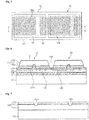
- Figure 5 is a schematic plan view of a light emitting device according to one exemplary embodiment of the present invention.
- Figure 6 is a cross-sectional view taken along line A-A in Figure 5 .
- Figures 7 to 12 are cross sectional-views illustrating a method of fabricating a light emitting device according to one exemplary embodiment of the present invention.
- Figure 13 is a cross-sectional view of a light emitting device according to another exemplary embodiment of the present invention.
- Figure 5 is a schematic plan view of a light emitting device according to one exemplary embodiment of the present invention
- Figure 6 is a cross-sectional view taken along line A-A in Figure 5 .
- the light emitting device includes a substrate 151, first light emitting cell S1 and a second light emitting cellS2, an isolation trench 161, and connectors 135. Further, the light emitting device may include holes 130a, an ohmic contact layer 131, an insulation layer 133, an isolation insulation layer 137, a adhesion layer 139, and a bonding metal 141. In some embodiments, the light emitting device may further include a protective insulation layer.
- the substrate 151 is distinguished from a growth substrate for growing compound semiconductors and is a substrate to be attached to the compound semiconductors which have been already grown.
- the substrate 151 may be a sapphire substrate, but is not limited thereto.
- the substrate 151 may be a different kind of insulation or conductive substrate.
- the light emitting cells S1, S2 are isolated from each other by the isolation trench 161.
- Each of the light emitting cells S1, S2 includes a semiconductor stack 130, which includes a first conductive type upper semiconductor layer 125, an active layer 127, and a second conductive type lower semiconductor layer 129.
- the active layer 127 is interposed between the first conductive type upper semiconductor layer 125 and the second conductive type lower semiconductor layer 129.
- Each of the light emitting cells S1, S2 includes a hole 130a formed through the second conductive type lower semiconductor layer 129 and the active layer 127 to expose the first conductive type upper semiconductor layer 125.
- the holes 130a are located at central regions of the light emitting cells S1, S2, respectively.
- Each of the light emitting cells S1, S2 may include a single hole 130a, but is not limited thereto. Alternatively, each of the light emitting cells S1, S2 may include a plurality of holes 130a.
- the active layer 127 and the upper and lower semiconductor layers 125, 129 may be formed of III-N based compound semiconductors, for example, (Al, Ga, In)N semiconductors.
- Each of the upper and lower semiconductor layers 125, 129 may be a single layer or multiple layers.
- the upper and/or lower semiconductor layers 125, 129 may include a contact layer and a clad layer.
- the upper and/or lower semiconductor layers 125, 129 may further include a supper lattice layer.
- the active layer 127 may have a single quantum well structure or a multi-quantum well structure.
- the first conductive type is n-type and the second conductive type is p-type.
- the upper semiconductor layers 125 may be formed of n-type semiconductor layers having relatively low resistance, it is possible to form relatively thick upper semiconductor layers 125. Accordingly, a roughened surface R can be easily formed on an upper surface of the upper semiconductor layer 125, thereby enhancing extraction efficiency of light produced in the active layer 127.
- the isolation trenches 161 are formed through the first conductive type upper semiconductor layer 125, active layer 127 and second conductive type lower semiconductor layer 129, so that inner walls of the isolation trenches 161 are formed of the semiconductor stack 130. Since all of the isolation trenches 161 may be formed with the same depth, an etching process for forming the isolation trenches 161 may be stably performed.
- the connectors 135 are located between the light emitting cells S1, S2 and the substrate 151 to electrically connect the light emitting cells S1, S2 to each other.
- the two connectors 135 5 are connected to one light emitting cell S1 or S2 and are electrically connected to the first conductive type upper semiconductor layer 125 and the second conductive type lower semiconductor layer 129 of the one light emitting cells S1 and S2, respectively.
- each of the connectors 135 electrically connects adjacent light emitting cells to each other.
- the connector 135 electrically connects the second conductive type lower semiconductor layer 129 of the first light emitting cell S1 to the first conductive type upper semiconductor layer 125 of the second light emitting cell S2.
- the connector 135 may be electrically connected to the first conductive type upper semiconductor layer 125 exposed in the hole 130a of the second light emitting cell.
- a plurality of light emitting cells may be connected in series to one another via the connectors 135 to form a series array of the light emitting cells, thereby providing a light emitting device which can be operated at high voltage.
- a plurality of series arrays may be provided and connected in reverse parallel to one another, thereby providing an AC light emitting device which can be operated by an AC power source.
- the ohmic contact layer 131 may contact to the second conductive type lower semiconductor layer 129.
- the ohmic contact layer 131 is formed over most of the second conductive type lower semiconductor layer 129 to assist current spreading in the light emitting cells S1, S2.
- the ohmic contact layer 131 may include a reflective metal layer and thus may reflect light directed from the light emitting cells S1, S2 towards the substrate 51.
- the connector 135 electrically connected to the second conductive type lower semiconductor layer 129 of the first light emitting cell S1 may be connected to the ohmic contact layer 131.
- the connector 135 is insulated from the second conductive type lower semiconductor layer 129 and the ohmic contact layer 131 of the second light emitting cell S2 while being electrically connected to the first conductive type upper semiconductor layer 125 of the second light emitting cell S2.
- the insulation layer 133 is interposed between the isolation trench 161 and the connector 135 to prevent the connector 135 from being exposed to the outside. Therefore, while the isolation trench 161 is formed by etching, it is possible to protect the connectors from etching damage.
- the insulation layer 133 is located on a sidewall of the holes 130a to prevent the connectors 135 from causing short circuit of the upper and lower semiconductor layers 125, 127. Further, the insulation layer 133 is interposed between the ohmic contact layer 131 and the connectors 135 to insulate the ohmic contact layer 131 and the connectors 135 from each other.
- the insulation layer on the holes 130a, the insulation layer for preventing etching damage, and the insulation layer on the ohmic contact layer 131 may be formed of a single insulation layer 133 and may include a distribution Bragg reflector (DBR). Alternatively, these insulation layers may be formed by different processes.
- DBR distribution Bragg reflector
- the bonding metal 141 may be interposed between the light emitting cells S1, S2 and the substrate 151.
- the bonding metal 141 may be formed of metallic materials, for example, Au/Sn, to bond the substrate 151 to the light emitting cells S1, S2.
- the isolation insulation layer 137 may be interposed between the light emitting cells S1, S2 and the bonding metal 141 to electrically insulate the connectors 135 from the bonding metal 141.
- the adhesion layer 139 for example, Cr/Au, may be formed under the isolation insulation layer 137 to enhance an adhesive force of the bonding metal 141.
- the first conductive type upper semiconductor layer 125 may include a roughened surface R. Further, a protective insulation layer (not shown) may cover the light emitting cells S1 and S2 to protect the light emitting cells. The protective insulation layer may fill the isolation trench 161.
- Figures 7 to 12 are cross-sectiona views illustrating a method of fabricating a light emitting device according to one exemplary embodiment of the present invention.
- a semiconductor stack 130 of compound semiconductor layers is formed on a sacrificial substrate 121.
- the sacrificial substrate 121 may be a sapphire substrate, but is not limited thereto. Alternatively, the sacrificial substrate 121 may be a heterogeneous substrate.
- the compound semiconductor layers may include a first conductive type semiconductor layer 125, a second conductive type semiconductor layer 129, and an active layer 127 interposed between the first and second conductive type semiconductor layers 125, 129.
- the first conductive type semiconductor layer 125 is located nearer to the sacrificial substrate 121.
- Each of the first and second conductive type layers 125, 129 may be a single layer or multiple layers.
- the active layer 127 may have a single quantum well structure or a multi-quantum well structure.
- These compound semiconductor layers 23, 25, 27 may be formed of III-N based compound semiconductors on the sacrificial substrate 121 by metal organic chemical vapor deposition (MOCVD) or molecular beam epitaxy (MBE).
- MOCVD metal organic chemical vapor deposition
- MBE molecular beam epitaxy
- a buffer layer (not shown) may be formed before forming the compound semiconductor layers.
- the buffer layer is employed to relieve lattice mismatch between the sacrificial substrate 121 and the compound semiconductor layers, and may be a gallium nitride-based material such as gallium nitride or aluminum nitride.
- Holes 130a are formed to expose the first conductive type semiconductor layer 125 by patterning the semiconductor stack 130.
- the holes 130a are formed at central regions of light emitting cells for connecting connectors to the first conductive type semiconductor layer 125.
- Side surfaces of the active layer 127 and the second conductive type semiconductor layer 129 are exposed on inner walls of the holes 130a.
- the compound semiconductor layers are subjected to patterning by photolithography and etching, which are very similar to a mesa etching process.
- the mesa etching process is generally performed to provide a mesh shape so as to isolate the second conductive type semiconductor layers 129 of the light emitting cells from each other, whereas the holes 130a are separated from each other in the embodiments of the invention. Accordingly, the holes 130a may be reduced in area to allow an isolation insulation layer and a bonding metal to be easily flattened, so that the substrate 151 can be stably attached to the semiconductor layers.
- an ohmic contact layer 131 may be formed on the second conductive type semiconductor layer 129.
- the ohmic contact layer 131 may form an ohmic contact with the second conductive type lower semiconductor layer 129.
- the ohmic contact layer 131 is formed on each of the light emitting cells and has an opening which exposes each of the holes 130a.
- the ohmic contact layer 131 may include a reflective metal layer.
- the ohmic contact layer 131 may include a barrier layer for protecting the reflective metal layer.
- An insulation layer 133 may be formed to cover a sidewall of the holes 130a while covering a portion of the ohmic contact layer 131.
- the insulation layer 133 covers the second conductive type semiconductor layer 129 located in a region between the light emitting cells.
- the insulation layer covering the sidewall of the holes 130a, the insulation layer on the ohmic contact layer 131 and the insulation layer located between the light emitting cells may be formed of the same material by the same process. Alternatively, these insulation layers may be formed by different processes.
- the insulation layer 133 may be formed of, for example, SiO 2 SiN, MgO, TaO, TiO 2 or polymer, and may include a distributed Bragg reflector (DBR).
- DBR distributed Bragg reflector
- connectors 135 are formed on the insulation layer 133.
- Each of the connectors 135 electrically connects the first conductive-type semiconductor layer 125 exposed in the hole 130a to the second conductive type semiconductor layer 129 in an adjacent light emitting cell region.
- the connector 135 electrically connected to the second conductive-type semiconductor layer 129 may be connected to the ohmic contact layer 131.
- an insulation layer 133 is interposed between the connector 135 and the ohmic contact layer 131.
- an isolation insulation layer 137 is formed substantially on an overall surface of the sacrificial substrate 121 on which the connectors 135 are formed.
- the isolation insulation layer 137 covers the connectors 135 and the insulation layer 133.
- the isolation insulation layer 137 may be formed of a silicon oxide film, a silicon nitride film, or the like. Further, the isolation insulation layer 137 may be a DBR with SiO 2 /TiO 2 periodically formed therein.
- An adhesion layer 139 may be formed on the isolation insulation layer 137 and a bonding metal 141 may be formed on the adhesion layer 139. Then, the substrate 151 may be bonded to the bonding metal 141.
- the bonding metal 141 may be formed of, for example, AuSn (80/20 wt%).
- the substrate 151 may have the same thermal expansion coefficient as that of the sacrificial substrate 121.
- the substrate 151 may be formed of a sapphire substrate, but is not limited thereto.
- the sacrificial substrate 121 is then removed and the first conductive type semiconductor layer 125 is exposed.
- the sacrificial substrate 121 may be removed via laser lift-off (LLO) or other mechanical or chemical techniques.
- LLO laser lift-off
- the buffer layer is also removed to expose the first conductive type semiconductor layer 125.
- an isolation trench 161 is formed to divide the semiconductor stack 130 into light emitting cells S1, S2.
- the isolation trench 161 is formed by etching the semiconductor stack 130 until the insulation layer 133 is exposed.
- the insulation layer 133 prevents the connectors 135 from being exposed.
- a sidewall of the isolation trench 161 is formed of the semiconductor stack 130, and the side surfaces of the first conductive type semiconductor layer 125, active layer and second conductive type semiconductor layer 127, 129 are exposed in the isolation trench.
- a roughened surface R may be formed on the first conductive type semiconductor layer 125 by a photo-enhanced chemical (PEC) etching or the like.
- PEC photo-enhanced chemical
- a protective insulation layer (not shown) and electrode pads (not shown) are formed on the first conductive semiconductor layers 125 and the substrate 151 is divided into light emitting device units each including the light emitting cells S1, S2, thereby providing a single chip light emitting device.
- Figure 13 is a cross-sectional view of a light emitting device according to another exemplary embodiment of the present invention.
- the light emitting device according to this embodiment has a similar structure to the light emitting device described with reference to Figures 5 and 6 .
- a DBR 170 is formed before the formation of an ohmic contact layer 171.
- the DBR 170 is interposed between the ohmic contact layer 171 and a second conductive type lower semiconductor layer 129.
- the DBR 170 may cover a sidewall in holes 130a and may be interposed between an isolation trench 161 and a connector 175.
- the DBR 170 may include through-holes 170a between the ohmic contact layer 171 and the second conductive type lower semiconductor layer 129, and the ohmic contact layer 171 may be connected to the second conductive type lower semiconductor layer 129 through the through-holes 170a.
- An insulation layer 173 is formed on some regions of the ohmic contact layer 171 and electrically insulates the connector 175 from the ohmic contact layer 171.
- the DBR 170 is formed on the sidewall in the holes 130a, on the region between the ohmic contact layer 171 and the second conductive type lower semiconductor layer 129, and on the region between the isolation trench 161 and the connector 175, thereby improving reflection of light produced in the light emitting cells S1, S2 and thus improving luminous efficiency.
Landscapes
- Led Devices (AREA)
Abstract
Description
- FIELD OF THE INVENTION
- The invention relates to a light emitting device and a method of fabricating the same and, more particularly, to a light emitting device which may be fabricated through application of a substrate lift-off process, and a method of fabricating the same.
- DESCRIPTION OF THE BACKGROUND
- A light emitting diode refers to a semiconductor device that has a p-n junction of semiconductors and emits light through electron-hole recombination. Such light emitting diodes are used in a wide range of applications, such as display devices, backlights, etc. Furthermore, the light emitting diodes have advantages of lower power consumption and longer lifetime than existing electric bulbs or fluorescent lamps, and application of the light emitting diodes, as a substitute for existing electric bulbs and fluorescent lamps, has been expanded to general illumination.
- In recent years, AC light emitting diodes directly connected to an AC power source to continuously emit light have been produced. One example of AC light emitting diodes directly connected to a high voltage AC power source for use is disclosed in PCT Publication No.
WO 2004/023568 (A1) - According to PCT Publication No.
WO 2004/023568 A1 - Since the AC-LED includes light emitting cells on the substrate used as a growth substrate, for example, on the sapphire substrate, there are limitations to the structure of the light emitting cells and enhancement of light extraction efficiency. To solve such problems, a method of fabricating an AC-LED through a substrate lift-off process is disclosed in Korean Patent No.
10-0599012 -
Figures 1 to 4 are cross-sectional views illustrating a conventional method of fabricating a light emitting device. - Referring to
Figure 1 , semiconductor layers including abuffer layer 23, an N-type semiconductor layer 25, anactive layer 27 and a P-type semiconductor layer 29 are formed on a sacrificial substrate 21. Further, afirst metal layer 31 is formed on the semiconductor layers and asecond metal layer 53 is formed on asubstrate 51 separate from the sacrificial substrate 21. Thefirst metal layer 31 may include a reflective metal layer. Thesecond metal layer 53 is bonded to thefirst metal layer 31 so that thesubstrate 51 is bonded to an upper portion of the semiconductor layers. - Referring to
Figure 2 , after bonding thesubstrate 51, the sacrificial substrate 21 is removed using a laser lift-off process. Further, after the sacrificial substrate 21 is removed, theremaining buffer layer 23 is removed and the surface of the N-type semiconductor layer 25 is exposed. - Referring to
Figure 3 , thesemiconductor layers metal layers metal patterns 40 separated from each other andlight emitting cells 30 located on themetal patterns 40. Each of thelight emitting cells 30 includes a P-type semiconductor layer 29a,active layer 27a and N-type semiconductor layer 25a, which are subjected to patterning. - Referring to
Figure 4 ,metal wires 57 are formed to electrically connect upper surfaces of thelight emitting cells 30 to themetal patterns 40 adjacent thereto. Themetal wires 57 connect thelight emitting cells 30 to each other to form series arrays of the light emitting cells. In order to connect themetal wires 57 to the light emitting cells,electrode pads 55 may be formed on the N-type semiconductor layers 25a, and electrode pads may also be formed on themetal patterns 40. Two or more series arrays may be formed and connected in reverse parallel to each other, thereby providing a light emitting diode which can be driven by an AC power source. - As such, the conventional method can improve heat dissipation of the light emitting device through appropriate selection of the
substrate 51 and can enhance light extraction efficiency via treatment of the surface of the N-type semiconductor layer 25a. Further, since thefirst metal layer 31 includes the reflective metal layer to reflect light, which is directed from thelight emitting cells 30 towards thesubstrate 51, thereby further improving luminous efficiency. - However, such a conventional method may cause short circuit between the N-
type semiconductor layer 25a and the P-type semiconductor layer 29a due to adhesion of metallic etching by-products to sidewalls of thelight emitting cells 30 during patterning of thesemiconductor layers metal layers semiconductor layers first metal layer 31 a is exposed and likely to be damaged by plasma. When thefirst metal layer 31 a includes the reflective metal layer such as Ag or A1, such etching damage is further deteriorated. The damage to the surface of themetal layer 31a by plasma deteriorates contact between thewires 57 or electrode pads and the metal layer, thereby causing device failure. - In the conventional method, the
first metal layer 31 may include the reflective metal layer and thus reflect light, which is directed from thelight emitting cells 30 towards the substrate. However, the reflective metal layer in a space between thelight emitting cells 30 is frequently damaged by etching or oxidation, deteriorating reflectivity thereof. Furthermore, since thesubstrate 51 is exposed on an area between themetal patterns 40, light can be absorbed by thesubstrate 51, thereby causing optical loss. - Moreover, since the
wires 57 are connected to an upper surface of the N-type semiconductor layer 25a, that is, a light emitting surface, light produced by theactive layer 25a can be absorbed by thewires 57 and/or theelectrode pads 55 on the light emitting surface, thereby causing optical loss. - Exemplary embodiments of the invention provide a light emitting device for high voltage operation, which may prevent electric short circuit in light emitting cells due to metallic etching by-products, and a method of fabricating the same.
- Further exemplary embodiments of the invention provide a light emitting device, which may reduce loss of light directed towards a substrate in a space between light emitting cells, and a method of fabricating the same.
- Further exemplary embodiments of the invention provide a light emitting device, which may reduce loss of light emitted from a light emitting surface to improve overall luminous efficiency, and a method of fabricating the same.
- Further exemplary embodiments of the invention provide a light emitting device, which may assist current spreading in light emitting cells, and a method of fabricating the same.
- Additional features of the invention will be set forth in the description which follows, and in part will be apparent from the description, or may be learned by practice of the invention.
- An exemplary embodiment of the present invention discloses a light emitting device. The light emitting device includes: a substrate; first and second light emitting cells, each including a first conductive type upper semiconductor layer, an active layer, a second conductive type lower semiconductor layer, and a hole formed through the second conductive type lower semiconductor layer and the active layer to expose the first conductive type upper semiconductor layer; and a connector located between the first and second light emitting cells and the substrate and electrically connecting the first and second light emitting cells to each other. The holes may be located at central regions of the first and second light emitting cells, respectively, and the connector may electrically connect the second conductive type lower semiconductor layer of the first light emitting cell to the first conductive type upper semiconductor layer exposed in the hole of the second light emitting cell.
- Since the connector is located between the substrate and the light emitting cells, it is possible to prevent loss of light by the connector. Further, since the holes are located at the central regions of the light emitting cells, the connector can be connected to the first conductive type upper semiconductor layers at the central regions, thereby allowing current spreading over a wide area of the light emitting cells.
- Furthermore, each of the first and second light emitting cells may include a single hole which exposes the first conductive type upper semiconductor layer, but is not limited thereto. Alternatively, each of the first and second light emitting cells may include a plurality of holes.
- The light emitting device may further include an isolation trench isolating the light emitting cells from each other and an insulation layer interposed between the isolation trench and the connector. When etching the semiconductor layers to form the isolation trench, the insulation layer prevents the connector from being exposed, so that the connector may be prevented from being damaged by etching.
- The insulation layer may include a distributed Bragg reflector (DBR). Accordingly, it is possible to reflect light, which is directed from a region between the light emitting cells towards the substrate, thereby further enhancing luminous efficiency.
- The isolation trench may be formed through the first conductive type upper semiconductor layer, active layer and second conductive type lower semiconductor layer. Namely, the isolation trench may be formed by etching the semiconductor layers including the first conductive type upper semiconductor layer, active layer and second conductive type lower semiconductor layer, thereby simplifying the process of forming the light emitting cells.
- The light emitting device may further include an insulation layer covering a sidewall of the holes. The insulation layer prevents the connector from causing short circuit of the first conductive type upper semiconductor layer and the second conductive type lower semiconductor layer. Furthermore, the insulation layer may include a DBR. Accordingly, it is possible to prevent light produced in the light emitting cells from being absorbed and lost by the connector in the hole.
- In some embodiments, the light emitting device may further include an ohmic contact layer which contacts the second conductive type lower semiconductor layer of each of the light emitting cells. Here, the connector is insulated from the ohmic contact layer of the second light emitting cell while being connected to the ohmic contact layer of the first light emitting cell. In some embodiments, an insulation layer may be interposed between the ohmic contact layer of the second light emitting cell and the connector, so that the connector may be insulated from the ohmic contact layer via the insulation layer.
- Further, a DBR may be interposed between the ohmic contact layer and the second conductive type lower semiconductor layer. Here, the DBR may include through-holes, through which the ohmic contact layer may be connected to the second conductive type lower semiconductor layer.
- An isolation insulation layer may be interposed between the connector and the substrate. The isolation insulation layer prevents electrical short circuit by isolating the bonding metal from the connector.
- Another exemplary embodiment of the present invention discloses a light emitting device. The light emitting device including: a substrate; a first light emitting cell including a first conductive type upper semiconductor layer, an active layer, a second conductive type lower semiconductor layer, and a hole formed through the second conductive type lower semiconductor layer and the active layer to expose the first conductive type upper semiconductor layer; a first connector electrically connected to the first conductive type upper semiconductor layer through the hole; and a second connector electrically connected to the second conductive type lower semiconductor layer. The hole may be located at a central region of the light emitting cell and the first connector may be electrically insulated from the second conductive type lower semiconductor layer. As such, the first and second connectors are disposed between the light emitting cells and the substrate to prevent optical loss, and the second connector is connected to the central region of the light emitting cell to assist current spreading in the light emitting cell.
- The first light emitting cell may include a plurality of holes exposing the first conductive type upper semiconductor layer.
- An insulation layer may be formed on a sidewall of the hole. The insulation layer prevents the second connector from causing short circuit of the first conductive type upper semiconductor layer and the second conductive type lower semiconductor layer. The insulation layer may include a DBR, thereby preventing light produced in the first light emitting cell from being lost by the second connector.
- In some embodiments, the light emitting cell may further include an ohmic contact layer which contacts the second conductive type lower semiconductor layer. The second connector may be connected to the ohmic contact layer. Furthermore, the ohmic contact layer may include a reflective metal layer to reflect light produced in the first light emitting cell towards an upper side when the light produced in the first light emitting cell is directed towards the substrate.
- In addition, an insulation layer may be interposed between the first connector and the ohmic contact layer. As a result, the first connector may be insulated from the ohmic contact layer via the insulation layer. The insulation layer may include a DBR.
- The light emitting device may further include a second light emitting cell including a first conductive type upper semiconductor layer, an active layer, and a second conductive type lower semiconductor layer, and the second connector may be electrically connected to the first conductive type upper semiconductor layer of the second light emitting cell.
- In some embodiments, the second light emitting cell may include a hole formed through the second conductive type lower semiconductor layer and the active layer to expose the first conductive type upper semiconductor layer, and the second connector may be electrically connected to the first conductive type upper semiconductor layer of the second light emitting cell through the hole.
- The first and second light emitting cells may be isolated from each other by an isolation trench, and an insulation layer may be interposed between the isolation trench and the second connector. The insulation layer may include a DBR.
- As such, the exemplary embodiments of the present invention provide light emitting devices for high voltage operation, which can prevent electrical short circuits in light emitting cells by preventing metallic etching by-products from being produced. Further, the light emitting device employs an insulation layer including a DBR to reflect light directed towards the substrate, thereby enhancing luminous efficiency. In addition, connectors connecting the light emitting cells are buried in the light emitting device, thereby preventing light emitted from a light emitting surface from being lost by the connectors. Further, the light emitting cells are formed at the central regions thereof with holes, through which the connectors are connected to the first conductive type upper semiconductor layers to assist current spreading in the light emitting cells.
- It is to be understood that both the foregoing general description and the following detailed description are exemplary and explanatory and are intended to provide further explanation of the invention as claimed.
- The accompanying drawings, which are included to provide a further understanding of the invention and are incorporated in and constitute a part of this specification, illustrate embodiments of the invention, and together with the description serve to explain the principles of the invention.
-
Figures 1 to 4 are cross-sectional views illustrating a conventional method of fabricating a light emitting device. -
Figure 5 is a schematic plan view of a light emitting device according to one exemplary embodiment of the present invention. -
Figure 6 is a cross-sectional view taken along line A-A inFigure 5 . -
Figures 7 to 12 are cross sectional-views illustrating a method of fabricating a light emitting device according to one exemplary embodiment of the present invention. -
Figure 13 is a cross-sectional view of a light emitting device according to another exemplary embodiment of the present invention. - The invention is described more fully hereinafter with reference to the accompanying drawings, in which exemplary embodiments of the invention are shown. This invention may, however, be embodied in many different forms and should not be construed as limited to the exemplary embodiments set forth herein. Rather, these exemplary embodiments are provided so that this disclosure is thorough and will fully convey the scope of the invention to those skilled in the art. In the drawings, the sizes and relative sizes of layers and regions may be exaggerated for clarity. Like reference numerals in the drawings denote like elements.
- It will be understood that when an element such as a layer, film, region or substrate is referred to as being "on" another element, it can be directly on the other element or intervening elements may also be present. In contrast, when an element is referred to as being "directly on" another element, there are no intervening elements present.
-
Figure 5 is a schematic plan view of a light emitting device according to one exemplary embodiment of the present invention, andFigure 6 is a cross-sectional view taken along line A-A inFigure 5 . - Referring to
Figures 5 and 6 , the light emitting device includes asubstrate 151, first light emitting cell S1 and a second light emitting cellS2, anisolation trench 161, andconnectors 135. Further, the light emitting device may includeholes 130a, anohmic contact layer 131, aninsulation layer 133, anisolation insulation layer 137, aadhesion layer 139, and abonding metal 141. In some embodiments, the light emitting device may further include a protective insulation layer. - The
substrate 151 is distinguished from a growth substrate for growing compound semiconductors and is a substrate to be attached to the compound semiconductors which have been already grown. Thesubstrate 151 may be a sapphire substrate, but is not limited thereto. Alternatively, thesubstrate 151 may be a different kind of insulation or conductive substrate. In particular, when using a sapphire substrate as the growth substrate for semiconductors, it is desirable that thesubstrate 151 be a sapphire substrate to have the same thermal expansion coefficient as the growth substrate. - The light emitting cells S1, S2 are isolated from each other by the
isolation trench 161. Each of the light emitting cells S1, S2 includes asemiconductor stack 130, which includes a first conductive typeupper semiconductor layer 125, anactive layer 127, and a second conductive typelower semiconductor layer 129. Theactive layer 127 is interposed between the first conductive typeupper semiconductor layer 125 and the second conductive typelower semiconductor layer 129. Each of the light emitting cells S1, S2 includes ahole 130a formed through the second conductive typelower semiconductor layer 129 and theactive layer 127 to expose the first conductive typeupper semiconductor layer 125. Theholes 130a are located at central regions of the light emitting cells S1, S2, respectively. Each of the light emitting cells S1, S2 may include asingle hole 130a, but is not limited thereto. Alternatively, each of the light emitting cells S1, S2 may include a plurality ofholes 130a. - The
active layer 127 and the upper and lower semiconductor layers 125, 129 may be formed of III-N based compound semiconductors, for example, (Al, Ga, In)N semiconductors. Each of the upper and lower semiconductor layers 125, 129 may be a single layer or multiple layers. In some embodiments, the upper and/or lower semiconductor layers 125, 129 may include a contact layer and a clad layer. In other embodiments, the upper and/or lower semiconductor layers 125, 129 may further include a supper lattice layer. Theactive layer 127 may have a single quantum well structure or a multi-quantum well structure. In some embodiments, the first conductive type is n-type and the second conductive type is p-type. Since the upper semiconductor layers 125 may be formed of n-type semiconductor layers having relatively low resistance, it is possible to form relatively thick upper semiconductor layers 125. Accordingly, a roughened surface R can be easily formed on an upper surface of theupper semiconductor layer 125, thereby enhancing extraction efficiency of light produced in theactive layer 127. - The
isolation trenches 161 are formed through the first conductive typeupper semiconductor layer 125,active layer 127 and second conductive typelower semiconductor layer 129, so that inner walls of theisolation trenches 161 are formed of thesemiconductor stack 130. Since all of theisolation trenches 161 may be formed with the same depth, an etching process for forming theisolation trenches 161 may be stably performed. - The
connectors 135 are located between the light emitting cells S1, S2 and thesubstrate 151 to electrically connect the light emitting cells S1, S2 to each other. The twoconnectors 135 5 are connected to one light emitting cell S1 or S2 and are electrically connected to the first conductive typeupper semiconductor layer 125 and the second conductive typelower semiconductor layer 129 of the one light emitting cells S1 and S2, respectively. Further, each of theconnectors 135 electrically connects adjacent light emitting cells to each other. For example, theconnector 135 electrically connects the second conductive typelower semiconductor layer 129 of the first light emitting cell S1 to the first conductive typeupper semiconductor layer 125 of the second light emitting cell S2. Here, theconnector 135 may be electrically connected to the first conductive typeupper semiconductor layer 125 exposed in thehole 130a of the second light emitting cell. - As such, a plurality of light emitting cells may be connected in series to one another via the
connectors 135 to form a series array of the light emitting cells, thereby providing a light emitting device which can be operated at high voltage. Further, a plurality of series arrays may be provided and connected in reverse parallel to one another, thereby providing an AC light emitting device which can be operated by an AC power source. - The
ohmic contact layer 131 may contact to the second conductive typelower semiconductor layer 129. Theohmic contact layer 131 is formed over most of the second conductive typelower semiconductor layer 129 to assist current spreading in the light emitting cells S1, S2. Theohmic contact layer 131 may include a reflective metal layer and thus may reflect light directed from the light emitting cells S1, S2 towards thesubstrate 51. Here, theconnector 135 electrically connected to the second conductive typelower semiconductor layer 129 of the first light emitting cell S1 may be connected to theohmic contact layer 131. Theconnector 135 is insulated from the second conductive typelower semiconductor layer 129 and theohmic contact layer 131 of the second light emitting cell S2 while being electrically connected to the first conductive typeupper semiconductor layer 125 of the second light emitting cell S2. - The
insulation layer 133 is interposed between theisolation trench 161 and theconnector 135 to prevent theconnector 135 from being exposed to the outside. Therefore, while theisolation trench 161 is formed by etching, it is possible to protect the connectors from etching damage. - The
insulation layer 133 is located on a sidewall of theholes 130a to prevent theconnectors 135 from causing short circuit of the upper and lower semiconductor layers 125, 127. Further, theinsulation layer 133 is interposed between theohmic contact layer 131 and theconnectors 135 to insulate theohmic contact layer 131 and theconnectors 135 from each other. - In this embodiment, the insulation layer on the
holes 130a, the insulation layer for preventing etching damage, and the insulation layer on theohmic contact layer 131 may be formed of asingle insulation layer 133 and may include a distribution Bragg reflector (DBR). Alternatively, these insulation layers may be formed by different processes. - The
bonding metal 141 may be interposed between the light emitting cells S1, S2 and thesubstrate 151. Thebonding metal 141 may be formed of metallic materials, for example, Au/Sn, to bond thesubstrate 151 to the light emitting cells S1, S2. Further, theisolation insulation layer 137 may be interposed between the light emitting cells S1, S2 and thebonding metal 141 to electrically insulate theconnectors 135 from thebonding metal 141. In some embodiments, theadhesion layer 139, for example, Cr/Au, may be formed under theisolation insulation layer 137 to enhance an adhesive force of thebonding metal 141. - The first conductive type
upper semiconductor layer 125 may include a roughened surface R. Further, a protective insulation layer (not shown) may cover the light emitting cells S1 and S2 to protect the light emitting cells. The protective insulation layer may fill theisolation trench 161. -
Figures 7 to 12 are cross-sectiona views illustrating a method of fabricating a light emitting device according to one exemplary embodiment of the present invention. - Referring to
Figure 7 , asemiconductor stack 130 of compound semiconductor layers is formed on asacrificial substrate 121. Thesacrificial substrate 121 may be a sapphire substrate, but is not limited thereto. Alternatively, thesacrificial substrate 121 may be a heterogeneous substrate. The compound semiconductor layers may include a first conductivetype semiconductor layer 125, a second conductivetype semiconductor layer 129, and anactive layer 127 interposed between the first and second conductive type semiconductor layers 125, 129. The first conductivetype semiconductor layer 125 is located nearer to thesacrificial substrate 121. Each of the first and second conductive type layers 125, 129 may be a single layer or multiple layers. Further, theactive layer 127 may have a single quantum well structure or a multi-quantum well structure. - These compound semiconductor layers 23, 25, 27 may be formed of III-N based compound semiconductors on the
sacrificial substrate 121 by metal organic chemical vapor deposition (MOCVD) or molecular beam epitaxy (MBE). - A buffer layer (not shown) may be formed before forming the compound semiconductor layers. The buffer layer is employed to relieve lattice mismatch between the
sacrificial substrate 121 and the compound semiconductor layers, and may be a gallium nitride-based material such as gallium nitride or aluminum nitride. -
Holes 130a are formed to expose the first conductivetype semiconductor layer 125 by patterning thesemiconductor stack 130. Theholes 130a are formed at central regions of light emitting cells for connecting connectors to the first conductivetype semiconductor layer 125. Side surfaces of theactive layer 127 and the second conductivetype semiconductor layer 129 are exposed on inner walls of theholes 130a. - To form the
holes 130, the compound semiconductor layers are subjected to patterning by photolithography and etching, which are very similar to a mesa etching process. However, the mesa etching process is generally performed to provide a mesh shape so as to isolate the second conductive type semiconductor layers 129 of the light emitting cells from each other, whereas theholes 130a are separated from each other in the embodiments of the invention. Accordingly, theholes 130a may be reduced in area to allow an isolation insulation layer and a bonding metal to be easily flattened, so that thesubstrate 151 can be stably attached to the semiconductor layers. - Referring to
Figure 8 , anohmic contact layer 131 may be formed on the second conductivetype semiconductor layer 129. Theohmic contact layer 131 may form an ohmic contact with the second conductive typelower semiconductor layer 129. Theohmic contact layer 131 is formed on each of the light emitting cells and has an opening which exposes each of theholes 130a. Theohmic contact layer 131 may include a reflective metal layer. In some embodiments, theohmic contact layer 131 may include a barrier layer for protecting the reflective metal layer. - An
insulation layer 133 may be formed to cover a sidewall of theholes 130a while covering a portion of theohmic contact layer 131. Theinsulation layer 133 covers the second conductivetype semiconductor layer 129 located in a region between the light emitting cells. The insulation layer covering the sidewall of theholes 130a, the insulation layer on theohmic contact layer 131 and the insulation layer located between the light emitting cells may be formed of the same material by the same process. Alternatively, these insulation layers may be formed by different processes. - The
insulation layer 133 may be formed of, for example, SiO2 SiN, MgO, TaO, TiO2 or polymer, and may include a distributed Bragg reflector (DBR). - Referring to
Figure 9 ,connectors 135 are formed on theinsulation layer 133. Each of theconnectors 135 electrically connects the first conductive-type semiconductor layer 125 exposed in thehole 130a to the second conductivetype semiconductor layer 129 in an adjacent light emitting cell region. Theconnector 135 electrically connected to the second conductive-type semiconductor layer 129 may be connected to theohmic contact layer 131. Here, it is desirable that theconnector 135 be insulated from theohmic contact layer 131 and the second conductivetype semiconductor layer 129 in some regions. To this end, aninsulation layer 133 is interposed between theconnector 135 and theohmic contact layer 131. - Referring to
Figure 10 , anisolation insulation layer 137 is formed substantially on an overall surface of thesacrificial substrate 121 on which theconnectors 135 are formed. Theisolation insulation layer 137 covers theconnectors 135 and theinsulation layer 133. Theisolation insulation layer 137 may be formed of a silicon oxide film, a silicon nitride film, or the like. Further, theisolation insulation layer 137 may be a DBR with SiO2/TiO2 periodically formed therein. Anadhesion layer 139 may be formed on theisolation insulation layer 137 and abonding metal 141 may be formed on theadhesion layer 139. Then, thesubstrate 151 may be bonded to thebonding metal 141. Thebonding metal 141 may be formed of, for example, AuSn (80/20 wt%). Thesubstrate 151 may have the same thermal expansion coefficient as that of thesacrificial substrate 121. In some embodiments, thesubstrate 151 may be formed of a sapphire substrate, but is not limited thereto. - Referring to
Figure 11 , thesacrificial substrate 121 is then removed and the first conductivetype semiconductor layer 125 is exposed. Thesacrificial substrate 121 may be removed via laser lift-off (LLO) or other mechanical or chemical techniques. Here, the buffer layer is also removed to expose the first conductivetype semiconductor layer 125. - Referring to
Figure 12 , anisolation trench 161 is formed to divide thesemiconductor stack 130 into light emitting cells S1, S2. Theisolation trench 161 is formed by etching thesemiconductor stack 130 until theinsulation layer 133 is exposed. Here, theinsulation layer 133 prevents theconnectors 135 from being exposed. A sidewall of theisolation trench 161 is formed of thesemiconductor stack 130, and the side surfaces of the first conductivetype semiconductor layer 125, active layer and second conductivetype semiconductor layer type semiconductor layer 125 by a photo-enhanced chemical (PEC) etching or the like. - Then, a protective insulation layer (not shown) and electrode pads (not shown) are formed on the first conductive semiconductor layers 125 and the
substrate 151 is divided into light emitting device units each including the light emitting cells S1, S2, thereby providing a single chip light emitting device. -
Figure 13 is a cross-sectional view of a light emitting device according to another exemplary embodiment of the present invention. - Referring to
Figure 13 , the light emitting device according to this embodiment has a similar structure to the light emitting device described with reference toFigures 5 and 6 . In this embodiment, however, aDBR 170 is formed before the formation of anohmic contact layer 171. - The
DBR 170 is interposed between theohmic contact layer 171 and a second conductive typelower semiconductor layer 129. TheDBR 170 may cover a sidewall inholes 130a and may be interposed between anisolation trench 161 and aconnector 175. - The
DBR 170 may include through-holes 170a between theohmic contact layer 171 and the second conductive typelower semiconductor layer 129, and theohmic contact layer 171 may be connected to the second conductive typelower semiconductor layer 129 through the through-holes 170a. - An
insulation layer 173 is formed on some regions of theohmic contact layer 171 and electrically insulates theconnector 175 from theohmic contact layer 171. - In this embodiment, the
DBR 170 is formed on the sidewall in theholes 130a, on the region between theohmic contact layer 171 and the second conductive typelower semiconductor layer 129, and on the region between theisolation trench 161 and theconnector 175, thereby improving reflection of light produced in the light emitting cells S1, S2 and thus improving luminous efficiency. - Although the invention has been illustrated with reference to some exemplary embodiments in conjunction with the drawings, it will be apparent to those skilled in the art that various modifications and changes can be made in the invention without departing from the spirit and scope of the invention. Therefore, it should be understood that the embodiments are provided by way of illustration only and are given to provide complete disclosure of the invention and to provide thorough understanding of the invention to those skilled in the art. Thus, it is intended that the invention covers the modifications and variations ofthis invention provided they come within the scope of the appended claims and their equivalents.
In the following paragraphs are depicted some embodiments according to the present invention. -
Paragraph 1. A light emitting device, comprising: a substrate; a first light emitting cell and a second light emitting cell, each including a first conductive type upper semiconductor layer, an active layer, a second conductive type lower semiconductor layer, and a hole formed through the second conductive type lower semiconductor layer and the active layer to expose the first conductive type upper semiconductor layer; and a connector located between the first and second light emitting cells and the substrate and electrically connecting the first and second light emitting cells to each other,
wherein the holes are located at central regions of the first and second light emitting cells, respectively, and the connector electrically connects the second conductive type lower semiconductor layer of the first light emitting cell to the first conductive type upper semiconductor layer exposed in the hole of the second light emitting cell. -
Paragraph 2. The light emitting device ofparagraph 1, further comprising: an isolation trench isolating the light emitting cells from each other; and an insulation layer interposed between the isolation trench and the connector. - Paragraph 3. The light emitting device of
paragraph 2, wherein the insulation layer comprises a DBR. - Paragraph 4. The light emitting device of
paragraph 2, wherein the isolation trench is formed through the first conductive upper semiconductor layer, active layer and second conductive type lower semiconductor layer. -
Paragraph 5. The light emitting device ofparagraph 1, further comprising: an insulation layer covering a sidewall of the holes. - Paragraph 6. The light emitting device of
paragraph 5, wherein the insulation layer comprises a DBR. - Paragraph 7. The light emitting device of
paragraph 1, further comprising: an ohmic contact layer which contacts the second conductive type lower semiconductor layer of each of the light emitting cells,
wherein the connector is insulated from the ohmic contact layer of the second light emitting cell while being connected to the ohmic contact layer of the first light emitting cell. - Paragraph 8. The light emitting device of paragraph 7, further comprising: an insulation layer interposed between the ohmic contact layer of the second light emitting cell and the connector.
- Paragraph 9. The light emitting device of paragraph 7, further comprising a DBR interposed between the ohmic contact layer and the second conductive type lower semiconductor layer, wherein the DBR includes through-holes and the ohmic contact layer is connected to the second conductive type lower semiconductor layer through the through-holes.
- Paragraph 10. The light emitting device of
paragraph 1, further comprising: an isolation insulation layer interposed between the connector and the substrate. - Paragraph 11. The light emitting device of
paragraph 1, wherein each of the light emitting cells comprises a plurality of holes exposing the first conductive type upper semiconductor layer. - Paragraph 12. A light emitting device comprising: a substrate; a first light emitting cell including a first conductive type upper semiconductor layer, an active layer, a second conductive type lower semiconductor layer, and a hole formed through the second conductive type lower semiconductor layer and the active layer to expose the first conductive type upper semiconductor layer;
a first connector electrically connected to the first conductive type upper semiconductor layer through the hole; and a second connector electrically connected to the second conductive type lower semiconductor layer, wherein the hole is located at a central region of the light emitting cell and the first connector is electrically insulated from the second conductive type lower semiconductor layer. - Paragraph 13. The light emitting device of paragraph 12, further comprising: an insulation layer formed on a sidewall of the hole, the insulation layer comprising a DBR.
- Paragraph 14. The light emitting device of paragraph 12, further comprising: an ohmic contact layer contacting the second conductive type lower semiconductor layer, wherein the second connector is connected to the ohmic contact layer.
- Paragraph 15. The light emitting device of paragraph 14, wherein the ohmic contact layer comprises a reflective metal layer.
- Paragraph 16. The light emitting device of paragraph 14, further comprising: an insulation layer interposed between the first connector and the ohmic contact layer.
- Paragraph 17. The light emitting device of paragraph 16, wherein the insulation layer comprises a DBR.
- Paragraph 18. The light emitting device of paragraph 12, further comprising: a second light emitting cell including a first conductive type upper semiconductor layer, an active layer and a second conductive type lower semiconductor layer, wherein the second connector is electrically connected to the first conductive upper semiconductor layer of the second light emitting cell.
- Paragraph 19. The light emitting device of paragraph 18, wherein the second light emitting cell comprises a hole formed through the second conductive type lower semiconductor layer and the active layer to expose the first conductive type upper semiconductor layer, and the second connector is electrically connected to the first conductive type upper semiconductor layer of the second light emitting cell through the hole.
- Paragraph 20. The light emitting device of paragraph 18, wherein the first and second light emitting cells are isolated from each other by an isolation trench and an insulation layer is interposed between the isolation trench and the second connector.
- Paragraph 21. The light emitting device of paragraph 20, wherein the insulation layer interposed between the isolation trench and the second connector comprises a DBR.
- Paragraph 22. The light emitting device of paragraph 12, wherein the first light emitting cell comprises a plurality of holes exposing the first conductive type upper semiconductor layer.
Claims (8)
- A light emitting device comprising:a substrate (151);a first light emitting cell (S1) including a first conductive type upper semiconductor layer (125), an active layer (127), a second conductive type lower semiconductor layer (129), and a hole (130a) formed through the second conductive type lower semiconductor layer (129) andthe active layer (127) to expose the first conductive type upper semiconductor layer (125);a first connector (135) electrically connected to the first conductive type upper semiconductor layer (125) through the hole (130a); anda second connector electrically connected to the second conductive type lower semiconductor layer (129),wherein the hole (130a) is located at a central region of the light emitting cell (S1) and the first connector (135) is electrically insulated from the second conductive type lower semiconductor layer (129),wherein an ohmic contact layer (131) contacting the second conductive type lower semiconductor layer (129), wherein the second connector is connected to the ohmic contact layer (131), wherein an insulation layer (133) interposed between the first connector (135) and the ohmic contact layer (131), wherein the insulation layer (133) comprises a DBR.
- The light emitting device of claim 1, further comprising:an insulation layer (133) formed on a sidewall of the hole (135a).
- The light emitting device of claim 1, wherein the ohmic contact layer (131) comprises a reflective metal layer.
- The light emitting device of claim 1, further comprising:a second light emitting cell (S2) including a first conductive type upper semiconductor layer (125), an active layer (127) and a second conductive type lower semiconductor layer (129), wherein the second connector is electrically connected to the first conductive upper semiconductor layer (125) of the second light emitting cell (S1).
- The light emitting device of claim 4, wherein the second light emitting cell (S2) comprises a hole (130a) formed through the second conductive type lower semiconductor layer (129) and the active layer (127) to expose the first conductive type upper semiconductor layer (125), and the second connector is electrically connected to the first conductive type upper semiconductor layer (125) of the second light emitting cell (S2) through the hole (130a).
- The light emitting device of claim 4, wherein the first and second light emitting cells (S1, S2) are isolated from each other by an isolation trench (161) and an insulation layer (133) is interposed between the isolation trench (161) and the second connector.
- The light emitting device of claim 6, wherein the insulation layer (133) interposed between the isolation trench (161) and the second connector comprises a DBR.
- The light emitting device of claim 1, wherein the first light emitting cell comprises a plurality of holes (130a) exposing the first conductive type upper semiconductor layer (125).
Applications Claiming Priority (2)
| Application Number | Priority Date | Filing Date | Title |
|---|---|---|---|
| KR1020090135309A KR101106151B1 (en) | 2009-12-31 | 2009-12-31 | Light emitting device and method of manufacturing the same |
| EP10188088.8A EP2341543B1 (en) | 2009-12-31 | 2010-10-19 | Light emitting device and method of fabricating the same |
Related Parent Applications (3)
| Application Number | Title | Priority Date | Filing Date |
|---|---|---|---|
| EP10188088.8A Division-Into EP2341543B1 (en) | 2009-12-31 | 2010-10-19 | Light emitting device and method of fabricating the same |
| EP10188088.8A Division EP2341543B1 (en) | 2009-12-31 | 2010-10-19 | Light emitting device and method of fabricating the same |
| EP10188088.8 Division | 2010-10-19 |
Publications (2)
| Publication Number | Publication Date |
|---|---|
| EP2455970A1 true EP2455970A1 (en) | 2012-05-23 |
| EP2455970B1 EP2455970B1 (en) | 2022-09-14 |
Family
ID=43824163
Family Applications (2)
| Application Number | Title | Priority Date | Filing Date |
|---|---|---|---|
| EP12154396.1A Active EP2455970B1 (en) | 2009-12-31 | 2010-10-19 | Light emitting device |
| EP10188088.8A Active EP2341543B1 (en) | 2009-12-31 | 2010-10-19 | Light emitting device and method of fabricating the same |
Family Applications After (1)
| Application Number | Title | Priority Date | Filing Date |
|---|---|---|---|
| EP10188088.8A Active EP2341543B1 (en) | 2009-12-31 | 2010-10-19 | Light emitting device and method of fabricating the same |
Country Status (6)
| Country | Link |
|---|---|
| US (3) | US8258533B2 (en) |
| EP (2) | EP2455970B1 (en) |
| JP (3) | JP5766429B2 (en) |
| KR (1) | KR101106151B1 (en) |
| CN (1) | CN102117821B (en) |
| TW (2) | TWI538265B (en) |
Cited By (2)
| Publication number | Priority date | Publication date | Assignee | Title |
|---|---|---|---|---|
| EP2728631A1 (en) * | 2012-11-05 | 2014-05-07 | Iljin Led Co., Ltd. | Semiconductor light emitting diode including thermally conductive substrate |
| CN105702821A (en) * | 2016-03-29 | 2016-06-22 | 苏州晶湛半导体有限公司 | Semiconductor light-emitting device and manufacturing method thereof |
Families Citing this family (67)
| Publication number | Priority date | Publication date | Assignee | Title |
|---|---|---|---|---|
| KR101692410B1 (en) * | 2010-07-26 | 2017-01-03 | 삼성전자 주식회사 | Light emitting device and method of manufacturing the same |
| TWI435477B (en) * | 2010-12-29 | 2014-04-21 | Lextar Electronics Corp | High brightness light emitting diode |
| WO2012123840A1 (en) * | 2011-03-14 | 2012-09-20 | Koninklijke Philips Electronics N.V. | Led having vertical contacts redistributed for flip chip mounting |
| TW201240147A (en) * | 2011-03-22 | 2012-10-01 | Hon Hai Prec Ind Co Ltd | Light-emitting semiconductor chip |
| TWI488331B (en) | 2011-03-23 | 2015-06-11 | 晶元光電股份有限公司 | Light-emitting diode array |
| DE102011016302B4 (en) | 2011-04-07 | 2026-01-15 | OSRAM Opto Semiconductors Gesellschaft mit beschränkter Haftung | Optoelectronic semiconductor chip |
| US10243121B2 (en) * | 2011-06-24 | 2019-03-26 | Cree, Inc. | High voltage monolithic LED chip with improved reliability |
| US9728676B2 (en) * | 2011-06-24 | 2017-08-08 | Cree, Inc. | High voltage monolithic LED chip |
| US8952395B2 (en) | 2011-07-26 | 2015-02-10 | Micron Technology, Inc. | Wafer-level solid state transducer packaging transducers including separators and associated systems and methods |
| US9299742B2 (en) | 2011-08-15 | 2016-03-29 | Micron Technology, Inc. | High-voltage solid-state transducers and associated systems and methods |
| US8497146B2 (en) | 2011-08-25 | 2013-07-30 | Micron Technology, Inc. | Vertical solid-state transducers having backside terminals and associated systems and methods |
| EP3364467B1 (en) | 2011-09-16 | 2020-02-26 | Seoul Viosys Co., Ltd. | Light emitting diode |
| KR101888604B1 (en) * | 2011-10-28 | 2018-08-14 | 엘지이노텍 주식회사 | Light emitting device and light emitting device package |
| KR101871372B1 (en) * | 2011-10-28 | 2018-08-02 | 엘지이노텍 주식회사 | Light emitting device |
| CN103094274B (en) * | 2011-11-01 | 2016-02-10 | 三星电子株式会社 | Semiconductor light-emitting apparatus |
| KR101868537B1 (en) * | 2011-11-07 | 2018-06-19 | 엘지이노텍 주식회사 | Light emitting device and light emitting device package including the device |
| KR101289793B1 (en) * | 2011-11-16 | 2013-07-26 | 한국광기술원 | Light emitting diode and method of fabricating the same |
| US8912020B2 (en) * | 2011-11-23 | 2014-12-16 | International Business Machines Corporation | Integrating active matrix inorganic light emitting diodes for display devices |
| JP5139576B1 (en) * | 2011-12-09 | 2013-02-06 | 株式会社東芝 | Manufacturing method of semiconductor light emitting device |
| DE102011056888A1 (en) | 2011-12-22 | 2013-06-27 | Osram Opto Semiconductors Gmbh | Display device and method for producing a display device |
| KR101297353B1 (en) * | 2011-12-26 | 2013-08-19 | 한국광기술원 | Light emitting diode |
| CN102593284B (en) * | 2012-03-05 | 2014-06-18 | 映瑞光电科技(上海)有限公司 | Methods for manufacturing isolation deep trench and high voltage LED chip |
| US9450152B2 (en) | 2012-05-29 | 2016-09-20 | Micron Technology, Inc. | Solid state transducer dies having reflective features over contacts and associated systems and methods |
| WO2014025195A1 (en) * | 2012-08-07 | 2014-02-13 | 서울바이오시스 주식회사 | Wafer level light-emitting diode array and method for manufacturing same |
| CN102820398B (en) * | 2012-08-31 | 2015-05-27 | 厦门大学 | Distributed Bragg reflection and small area metal contact composite three-dimensional electrode |
| DE102012220909A1 (en) | 2012-09-27 | 2014-05-15 | Osram Opto Semiconductors Gmbh | Method for separating regions of a semiconductor layer |
| JP5924231B2 (en) * | 2012-10-24 | 2016-05-25 | 日亜化学工業株式会社 | Semiconductor light emitting device |
| US9196807B2 (en) * | 2012-10-24 | 2015-11-24 | Nichia Corporation | Light emitting element |
| KR102037865B1 (en) * | 2013-02-01 | 2019-10-30 | 삼성전자주식회사 | Semiconductor light emitting device and method thereof |
| KR102065390B1 (en) * | 2013-02-15 | 2020-01-13 | 엘지이노텍 주식회사 | Light emitting device, light emitting device package, and light unit |
| JP2014179469A (en) * | 2013-03-14 | 2014-09-25 | Toshiba Corp | Semiconductor light-emitting element, light-emitting device, and method of manufacturing semiconductor light-emitting device |
| DE102013102667A1 (en) * | 2013-03-15 | 2014-10-02 | Osram Opto Semiconductors Gmbh | display device |
| DE102013103079A1 (en) * | 2013-03-26 | 2014-10-02 | Osram Opto Semiconductors Gmbh | Optoelectronic semiconductor chip and method for producing an optoelectronic semiconductor chip |
| EP2989664B1 (en) * | 2013-04-23 | 2019-06-12 | Lumileds Holding B.V. | Side interconnect for light emitting device |
| KR102078365B1 (en) | 2013-07-01 | 2020-04-03 | 삼성디스플레이 주식회사 | Organic light emitting diode device |
| DE102013107531A1 (en) * | 2013-07-16 | 2015-01-22 | Osram Opto Semiconductors Gmbh | Optoelectronic semiconductor chip |
| KR101480537B1 (en) * | 2013-09-12 | 2015-01-09 | 한국광기술원 | Light emitting diode apparatus |
| JP2015177031A (en) * | 2014-03-14 | 2015-10-05 | スタンレー電気株式会社 | Light emitting device |
| KR102175345B1 (en) * | 2014-06-11 | 2020-11-06 | 엘지이노텍 주식회사 | Light emitting device and lighting system |
| JP6351520B2 (en) | 2014-08-07 | 2018-07-04 | 株式会社東芝 | Semiconductor light emitting device |
| JP6462274B2 (en) | 2014-08-21 | 2019-01-30 | 株式会社東芝 | Semiconductor light emitting device |
| KR102282141B1 (en) | 2014-09-02 | 2021-07-28 | 삼성전자주식회사 | Semiconductor light emitting device |
| KR20160037060A (en) * | 2014-09-26 | 2016-04-05 | 서울바이오시스 주식회사 | Light emitting device and method for fabricating the same |
| KR102189133B1 (en) * | 2014-10-17 | 2020-12-09 | 엘지이노텍 주식회사 | Light emitting device and light emitting device package |
| TWI568026B (en) * | 2014-11-04 | 2017-01-21 | 錼創科技股份有限公司 | Illuminating device |
| KR102347456B1 (en) * | 2015-03-09 | 2022-01-07 | 서울바이오시스 주식회사 | Semiconductor light emitting diode |
| US10658546B2 (en) * | 2015-01-21 | 2020-05-19 | Cree, Inc. | High efficiency LEDs and methods of manufacturing |
| KR102237152B1 (en) * | 2015-02-23 | 2021-04-07 | 엘지이노텍 주식회사 | Light emitting diode and lighting unit |
| TWI583020B (en) * | 2015-07-06 | 2017-05-11 | 隆達電子股份有限公司 | Light-emitting element and light-emitting device |
| JP2017059645A (en) * | 2015-09-15 | 2017-03-23 | 株式会社東芝 | Semiconductor light emitting device |
| DE102016123013A1 (en) * | 2016-11-29 | 2018-05-30 | Osram Opto Semiconductors Gmbh | Display device with a plurality of separately operable pixels |
| US11177417B2 (en) * | 2017-02-13 | 2021-11-16 | Nichia Corporation | Light emitting device including phosphor layer with protrusions and recesses and method for manufacturing same |
| JP6645486B2 (en) | 2017-02-13 | 2020-02-14 | 日亜化学工業株式会社 | Light emitting device and method of manufacturing the same |
| KR102385571B1 (en) * | 2017-03-31 | 2022-04-12 | 삼성전자주식회사 | Semiconductor light emitting device |
| JP6888224B2 (en) * | 2017-10-16 | 2021-06-16 | 住友電工デバイス・イノベーション株式会社 | Manufacturing method of semiconductor devices |
| FR3086100B1 (en) * | 2018-09-13 | 2022-08-12 | Commissariat Energie Atomique | METHOD FOR MANUFACTURING AN OPTOELECTRONIC DEVICE COMPRISING A PLURALITY OF DIODES |
| JP7096489B2 (en) * | 2018-09-20 | 2022-07-06 | 日亜化学工業株式会社 | Manufacturing method of semiconductor device |
| CN109891610A (en) * | 2018-10-11 | 2019-06-14 | 厦门市三安光电科技有限公司 | A kind of light-emitting diode and preparation method thereof |
| CN110731016B (en) * | 2018-11-13 | 2024-02-09 | 泉州三安半导体科技有限公司 | Light emitting diode |
| JP7253994B2 (en) * | 2019-07-23 | 2023-04-07 | 株式会社ディスコ | How to relocate optical devices |
| DE102019121580A1 (en) * | 2019-08-09 | 2021-02-11 | OSRAM Opto Semiconductors Gesellschaft mit beschränkter Haftung | COMPONENT WITH REDUCED ABSORPTION AND PROCESS FOR MANUFACTURING A COMPONENT |
| US11489089B2 (en) | 2020-06-19 | 2022-11-01 | Lextar Electronics Corporation | Light emitting device with two vertically-stacked light emitting cells |
| DE102021201131A1 (en) * | 2021-02-08 | 2022-08-11 | OSRAM Opto Semiconductors Gesellschaft mit beschränkter Haftung | OPTOELECTRONIC SEMICONDUCTOR COMPONENT WITH A GOLD LAYER IN THE REGION |
| CN115483323A (en) * | 2021-05-31 | 2022-12-16 | 京东方科技集团股份有限公司 | Light-emitting device, light-emitting substrate, and manufacturing method of light-emitting device |
| CN115799294A (en) * | 2022-11-29 | 2023-03-14 | 厦门三安光电有限公司 | Light-emitting element, light-emitting assembly and manufacturing method |
| CN115732533A (en) * | 2022-11-29 | 2023-03-03 | 厦门三安光电有限公司 | Light-emitting component, light-emitting element and manufacturing method |
| DE112023004992T5 (en) * | 2022-11-30 | 2025-09-18 | Nichia Corporation | Manufacturing method for a light-emitting element and light-emitting element |
Citations (8)
| Publication number | Priority date | Publication date | Assignee | Title |
|---|---|---|---|---|
| JP2004047504A (en) * | 2002-07-08 | 2004-02-12 | Korai Kagi Kofun Yugenkoshi | Light-emitting diode having enhanced emission efficiency |
| WO2004023568A1 (en) | 2002-08-29 | 2004-03-18 | Nitride Semiconductors Co.,Ltd. | Light-emitting device having light-emitting elements |
| WO2005081319A1 (en) * | 2004-02-20 | 2005-09-01 | Osram Opto Semiconductors Gmbh | Optoelectronic component, device comprising a plurality of optoelectronic components, and method for the production of an optoelectronic component |
| KR100599012B1 (en) | 2005-06-29 | 2006-07-12 | 서울옵토디바이스주식회사 | Light Emitting Diode Having Thermally Conductive Substrate And Method Of Manufacturing The Same |
| DE102007022947A1 (en) * | 2007-04-26 | 2008-10-30 | Osram Opto Semiconductors Gmbh | Optoelectronic semiconductor body and method for producing such |
| DE102008011848A1 (en) * | 2008-02-29 | 2009-09-03 | Osram Opto Semiconductors Gmbh | Optoelectronic semiconductor body and method for producing such |
| WO2009106063A1 (en) * | 2008-02-29 | 2009-09-03 | Osram Opto Semiconductors Gmbh | Monolithic, optoelectronic semi-conductor body and method for the production thereof |
| DE102008032318A1 (en) * | 2008-03-31 | 2009-10-01 | Osram Opto Semiconductors Gmbh | Optoelectronic semiconductor chip and method for producing such |
Family Cites Families (9)
| Publication number | Priority date | Publication date | Assignee | Title |
|---|---|---|---|---|
| US20020017652A1 (en) * | 2000-08-08 | 2002-02-14 | Stefan Illek | Semiconductor chip for optoelectronics |
| CN1202578C (en) * | 2001-12-07 | 2005-05-18 | 洲磊科技股份有限公司 | Formation of semiconductor elements with metal substrates |
| EP2290715B1 (en) * | 2002-08-01 | 2019-01-23 | Nichia Corporation | Semiconductor light-emitting device, method for manufacturing the same, and light-emitting apparatus including the same |
| JP3904571B2 (en) * | 2004-09-02 | 2007-04-11 | ローム株式会社 | Semiconductor light emitting device |
| KR100805324B1 (en) | 2006-05-17 | 2008-02-20 | (주)더리즈 | Light emitting diode for enhancing efficiency |
| JP5171016B2 (en) * | 2006-10-27 | 2013-03-27 | キヤノン株式会社 | Semiconductor member, manufacturing method of semiconductor article, and LED array using the manufacturing method |
| CN101335315B (en) * | 2007-06-26 | 2010-09-22 | 普瑞光电股份有限公司 | Light-emitting component having improved electrode construction |
| KR100891761B1 (en) * | 2007-10-19 | 2009-04-07 | 삼성전기주식회사 | Semiconductor light emitting device, manufacturing method thereof and semiconductor light emitting device package using same |
| KR100986570B1 (en) * | 2009-08-31 | 2010-10-07 | 엘지이노텍 주식회사 | Semiconductor light emitting device and fabrication method thereof |
-
2009
- 2009-12-31 KR KR1020090135309A patent/KR101106151B1/en active Active
-
2010
- 2010-10-19 EP EP12154396.1A patent/EP2455970B1/en active Active
- 2010-10-19 EP EP10188088.8A patent/EP2341543B1/en active Active
- 2010-11-19 JP JP2010258828A patent/JP5766429B2/en active Active
- 2010-11-19 US US12/950,676 patent/US8258533B2/en active Active
- 2010-12-14 TW TW103119004A patent/TWI538265B/en active
- 2010-12-14 TW TW099143755A patent/TWI445219B/en not_active IP Right Cessation
- 2010-12-30 CN CN2010106223876A patent/CN102117821B/en active Active
-
2011
- 2011-03-31 US US13/077,395 patent/US8294170B2/en active Active
- 2011-09-22 US US13/240,501 patent/US8324650B2/en active Active
-
2013
- 2013-12-26 JP JP2013268681A patent/JP2014078750A/en not_active Withdrawn
-
2015
- 2015-09-28 JP JP2015189382A patent/JP6087409B2/en active Active
Patent Citations (8)
| Publication number | Priority date | Publication date | Assignee | Title |
|---|---|---|---|---|
| JP2004047504A (en) * | 2002-07-08 | 2004-02-12 | Korai Kagi Kofun Yugenkoshi | Light-emitting diode having enhanced emission efficiency |
| WO2004023568A1 (en) | 2002-08-29 | 2004-03-18 | Nitride Semiconductors Co.,Ltd. | Light-emitting device having light-emitting elements |
| WO2005081319A1 (en) * | 2004-02-20 | 2005-09-01 | Osram Opto Semiconductors Gmbh | Optoelectronic component, device comprising a plurality of optoelectronic components, and method for the production of an optoelectronic component |
| KR100599012B1 (en) | 2005-06-29 | 2006-07-12 | 서울옵토디바이스주식회사 | Light Emitting Diode Having Thermally Conductive Substrate And Method Of Manufacturing The Same |
| DE102007022947A1 (en) * | 2007-04-26 | 2008-10-30 | Osram Opto Semiconductors Gmbh | Optoelectronic semiconductor body and method for producing such |
| DE102008011848A1 (en) * | 2008-02-29 | 2009-09-03 | Osram Opto Semiconductors Gmbh | Optoelectronic semiconductor body and method for producing such |
| WO2009106063A1 (en) * | 2008-02-29 | 2009-09-03 | Osram Opto Semiconductors Gmbh | Monolithic, optoelectronic semi-conductor body and method for the production thereof |
| DE102008032318A1 (en) * | 2008-03-31 | 2009-10-01 | Osram Opto Semiconductors Gmbh | Optoelectronic semiconductor chip and method for producing such |
Cited By (2)
| Publication number | Priority date | Publication date | Assignee | Title |
|---|---|---|---|---|
| EP2728631A1 (en) * | 2012-11-05 | 2014-05-07 | Iljin Led Co., Ltd. | Semiconductor light emitting diode including thermally conductive substrate |
| CN105702821A (en) * | 2016-03-29 | 2016-06-22 | 苏州晶湛半导体有限公司 | Semiconductor light-emitting device and manufacturing method thereof |
Also Published As
| Publication number | Publication date |
|---|---|
| KR101106151B1 (en) | 2012-01-20 |
| US8324650B2 (en) | 2012-12-04 |
| JP2014078750A (en) | 2014-05-01 |
| US8294170B2 (en) | 2012-10-23 |
| EP2341543A1 (en) | 2011-07-06 |
| US20120007044A1 (en) | 2012-01-12 |
| EP2341543B1 (en) | 2014-02-12 |
| TWI445219B (en) | 2014-07-11 |
| TW201442305A (en) | 2014-11-01 |
| US8258533B2 (en) | 2012-09-04 |
| JP6087409B2 (en) | 2017-03-01 |
| JP2016021591A (en) | 2016-02-04 |
| US20110156064A1 (en) | 2011-06-30 |
| TW201131835A (en) | 2011-09-16 |
| EP2455970B1 (en) | 2022-09-14 |
| CN102117821A (en) | 2011-07-06 |
| JP2011139038A (en) | 2011-07-14 |
| CN102117821B (en) | 2013-12-18 |
| TWI538265B (en) | 2016-06-11 |
| US20110180820A1 (en) | 2011-07-28 |
| KR20110078484A (en) | 2011-07-07 |
| JP5766429B2 (en) | 2015-08-19 |
Similar Documents
| Publication | Publication Date | Title |
|---|---|---|
| EP2341543B1 (en) | Light emitting device and method of fabricating the same | |
| US8383433B2 (en) | Light emitting diode and method of fabricating the same | |
| US8648369B2 (en) | Light emitting device and method of fabricating the same | |
| KR101017395B1 (en) | Light emitting device having a plurality of light emitting cells and method of manufacturing same | |
| KR100999733B1 (en) | Light emitting device, light emitting device manufacturing method and light emitting device package | |
| KR101115535B1 (en) | Light emitting diode with a metal reflection layer expanded and method for manufacturing the same | |
| KR101093117B1 (en) | Light emitting device for AC and method of manufacturing same | |
| KR101587539B1 (en) | Light emitting device having plurality of light emitting cells and method of fabricating the same | |
| KR101115570B1 (en) | Light emitting device and method of fabricating the same | |
| KR20100075420A (en) | Light emitting device having plurality of light emitting cells and method of fabricating the same | |
| KR101115539B1 (en) | Light emitting device and method of fabricating the same | |
| KR101171327B1 (en) | Light emitting device and method of fabricating the same | |
| KR101138977B1 (en) | Light emitting device and method of fabricating the same | |
| KR101735672B1 (en) | A light emitting device and a light emitting device package | |
| KR20120039953A (en) | A light emitting device |
Legal Events
| Date | Code | Title | Description |
|---|---|---|---|
| PUAI | Public reference made under article 153(3) epc to a published international application that has entered the european phase |
Free format text: ORIGINAL CODE: 0009012 |
|
| 17P | Request for examination filed |
Effective date: 20120208 |
|
| AC | Divisional application: reference to earlier application |
Ref document number: 2341543 Country of ref document: EP Kind code of ref document: P |
|
| AK | Designated contracting states |
Kind code of ref document: A1 Designated state(s): AL AT BE BG CH CY CZ DE DK EE ES FI FR GB GR HR HU IE IS IT LI LT LU LV MC MK MT NL NO PL PT RO RS SE SI SK SM TR |
|
| AX | Request for extension of the european patent |
Extension state: BA ME |
|
| RAP1 | Party data changed (applicant data changed or rights of an application transferred) |
Owner name: SEOUL VIOSYS CO., LTD |
|
| STAA | Information on the status of an ep patent application or granted ep patent |
Free format text: STATUS: EXAMINATION IS IN PROGRESS |
|
| 17Q | First examination report despatched |
Effective date: 20181010 |
|
| REG | Reference to a national code |
Ref country code: DE Ref legal event code: R079 Ref document number: 602010068468 Country of ref document: DE Free format text: PREVIOUS MAIN CLASS: H01L0027150000 Ipc: H01L0025075000 |
|
| RIC1 | Information provided on ipc code assigned before grant |
Ipc: H01L 33/62 20100101ALI20220125BHEP Ipc: H01L 33/38 20100101ALI20220125BHEP Ipc: H01L 33/22 20100101ALI20220125BHEP Ipc: H01L 25/075 20060101AFI20220125BHEP |
|
| GRAP | Despatch of communication of intention to grant a patent |
Free format text: ORIGINAL CODE: EPIDOSNIGR1 |
|
| STAA | Information on the status of an ep patent application or granted ep patent |
Free format text: STATUS: GRANT OF PATENT IS INTENDED |
|
| INTG | Intention to grant announced |
Effective date: 20220329 |
|
| GRAS | Grant fee paid |
Free format text: ORIGINAL CODE: EPIDOSNIGR3 |
|
| GRAA | (expected) grant |
Free format text: ORIGINAL CODE: 0009210 |
|
| STAA | Information on the status of an ep patent application or granted ep patent |
Free format text: STATUS: THE PATENT HAS BEEN GRANTED |
|
| AC | Divisional application: reference to earlier application |
Ref document number: 2341543 Country of ref document: EP Kind code of ref document: P |
|
| AK | Designated contracting states |
Kind code of ref document: B1 Designated state(s): AL AT BE BG CH CY CZ DE DK EE ES FI FR GB GR HR HU IE IS IT LI LT LU LV MC MK MT NL NO PL PT RO RS SE SI SK SM TR |
|
| REG | Reference to a national code |
Ref country code: GB Ref legal event code: FG4D |
|
| REG | Reference to a national code |
Ref country code: CH Ref legal event code: EP |
|
| REG | Reference to a national code |
Ref country code: DE Ref legal event code: R096 Ref document number: 602010068468 Country of ref document: DE |
|
| REG | Reference to a national code |
Ref country code: IE Ref legal event code: FG4D |
|
| REG | Reference to a national code |
Ref country code: AT Ref legal event code: REF Ref document number: 1519238 Country of ref document: AT Kind code of ref document: T Effective date: 20221015 |
|
| REG | Reference to a national code |
Ref country code: LT Ref legal event code: MG9D |
|
| REG | Reference to a national code |
Ref country code: NL Ref legal event code: MP Effective date: 20220914 |
|
| PG25 | Lapsed in a contracting state [announced via postgrant information from national office to epo] |
Ref country code: SE Free format text: LAPSE BECAUSE OF FAILURE TO SUBMIT A TRANSLATION OF THE DESCRIPTION OR TO PAY THE FEE WITHIN THE PRESCRIBED TIME-LIMIT Effective date: 20220914 Ref country code: RS Free format text: LAPSE BECAUSE OF FAILURE TO SUBMIT A TRANSLATION OF THE DESCRIPTION OR TO PAY THE FEE WITHIN THE PRESCRIBED TIME-LIMIT Effective date: 20220914 Ref country code: NO Free format text: LAPSE BECAUSE OF FAILURE TO SUBMIT A TRANSLATION OF THE DESCRIPTION OR TO PAY THE FEE WITHIN THE PRESCRIBED TIME-LIMIT Effective date: 20221214 Ref country code: LV Free format text: LAPSE BECAUSE OF FAILURE TO SUBMIT A TRANSLATION OF THE DESCRIPTION OR TO PAY THE FEE WITHIN THE PRESCRIBED TIME-LIMIT Effective date: 20220914 Ref country code: LT Free format text: LAPSE BECAUSE OF FAILURE TO SUBMIT A TRANSLATION OF THE DESCRIPTION OR TO PAY THE FEE WITHIN THE PRESCRIBED TIME-LIMIT Effective date: 20220914 Ref country code: FI Free format text: LAPSE BECAUSE OF FAILURE TO SUBMIT A TRANSLATION OF THE DESCRIPTION OR TO PAY THE FEE WITHIN THE PRESCRIBED TIME-LIMIT Effective date: 20220914 |
|
| REG | Reference to a national code |
Ref country code: AT Ref legal event code: MK05 Ref document number: 1519238 Country of ref document: AT Kind code of ref document: T Effective date: 20220914 |
|
| PG25 | Lapsed in a contracting state [announced via postgrant information from national office to epo] |
Ref country code: HR Free format text: LAPSE BECAUSE OF FAILURE TO SUBMIT A TRANSLATION OF THE DESCRIPTION OR TO PAY THE FEE WITHIN THE PRESCRIBED TIME-LIMIT Effective date: 20220914 Ref country code: GR Free format text: LAPSE BECAUSE OF FAILURE TO SUBMIT A TRANSLATION OF THE DESCRIPTION OR TO PAY THE FEE WITHIN THE PRESCRIBED TIME-LIMIT Effective date: 20221215 |
|
| PG25 | Lapsed in a contracting state [announced via postgrant information from national office to epo] |
Ref country code: SM Free format text: LAPSE BECAUSE OF FAILURE TO SUBMIT A TRANSLATION OF THE DESCRIPTION OR TO PAY THE FEE WITHIN THE PRESCRIBED TIME-LIMIT Effective date: 20220914 Ref country code: RO Free format text: LAPSE BECAUSE OF FAILURE TO SUBMIT A TRANSLATION OF THE DESCRIPTION OR TO PAY THE FEE WITHIN THE PRESCRIBED TIME-LIMIT Effective date: 20220914 Ref country code: PT Free format text: LAPSE BECAUSE OF FAILURE TO SUBMIT A TRANSLATION OF THE DESCRIPTION OR TO PAY THE FEE WITHIN THE PRESCRIBED TIME-LIMIT Effective date: 20230116 Ref country code: ES Free format text: LAPSE BECAUSE OF FAILURE TO SUBMIT A TRANSLATION OF THE DESCRIPTION OR TO PAY THE FEE WITHIN THE PRESCRIBED TIME-LIMIT Effective date: 20220914 Ref country code: CZ Free format text: LAPSE BECAUSE OF FAILURE TO SUBMIT A TRANSLATION OF THE DESCRIPTION OR TO PAY THE FEE WITHIN THE PRESCRIBED TIME-LIMIT Effective date: 20220914 Ref country code: AT Free format text: LAPSE BECAUSE OF FAILURE TO SUBMIT A TRANSLATION OF THE DESCRIPTION OR TO PAY THE FEE WITHIN THE PRESCRIBED TIME-LIMIT Effective date: 20220914 |
|
| PG25 | Lapsed in a contracting state [announced via postgrant information from national office to epo] |
Ref country code: SK Free format text: LAPSE BECAUSE OF FAILURE TO SUBMIT A TRANSLATION OF THE DESCRIPTION OR TO PAY THE FEE WITHIN THE PRESCRIBED TIME-LIMIT Effective date: 20220914 Ref country code: PL Free format text: LAPSE BECAUSE OF FAILURE TO SUBMIT A TRANSLATION OF THE DESCRIPTION OR TO PAY THE FEE WITHIN THE PRESCRIBED TIME-LIMIT Effective date: 20220914 Ref country code: IS Free format text: LAPSE BECAUSE OF FAILURE TO SUBMIT A TRANSLATION OF THE DESCRIPTION OR TO PAY THE FEE WITHIN THE PRESCRIBED TIME-LIMIT Effective date: 20230114 Ref country code: EE Free format text: LAPSE BECAUSE OF FAILURE TO SUBMIT A TRANSLATION OF THE DESCRIPTION OR TO PAY THE FEE WITHIN THE PRESCRIBED TIME-LIMIT Effective date: 20220914 |
|
| REG | Reference to a national code |
Ref country code: CH Ref legal event code: PL |
|
| REG | Reference to a national code |
Ref country code: DE Ref legal event code: R097 Ref document number: 602010068468 Country of ref document: DE |
|
| REG | Reference to a national code |
Ref country code: BE Ref legal event code: MM Effective date: 20221031 |
|
| PG25 | Lapsed in a contracting state [announced via postgrant information from national office to epo] |
Ref country code: NL Free format text: LAPSE BECAUSE OF FAILURE TO SUBMIT A TRANSLATION OF THE DESCRIPTION OR TO PAY THE FEE WITHIN THE PRESCRIBED TIME-LIMIT Effective date: 20220914 Ref country code: MC Free format text: LAPSE BECAUSE OF FAILURE TO SUBMIT A TRANSLATION OF THE DESCRIPTION OR TO PAY THE FEE WITHIN THE PRESCRIBED TIME-LIMIT Effective date: 20220914 Ref country code: LU Free format text: LAPSE BECAUSE OF NON-PAYMENT OF DUE FEES Effective date: 20221019 Ref country code: AL Free format text: LAPSE BECAUSE OF FAILURE TO SUBMIT A TRANSLATION OF THE DESCRIPTION OR TO PAY THE FEE WITHIN THE PRESCRIBED TIME-LIMIT Effective date: 20220914 |
|
| PLBE | No opposition filed within time limit |
Free format text: ORIGINAL CODE: 0009261 |
|
| STAA | Information on the status of an ep patent application or granted ep patent |
Free format text: STATUS: NO OPPOSITION FILED WITHIN TIME LIMIT |
|
| PG25 | Lapsed in a contracting state [announced via postgrant information from national office to epo] |
Ref country code: LI Free format text: LAPSE BECAUSE OF NON-PAYMENT OF DUE FEES Effective date: 20221031 Ref country code: DK Free format text: LAPSE BECAUSE OF FAILURE TO SUBMIT A TRANSLATION OF THE DESCRIPTION OR TO PAY THE FEE WITHIN THE PRESCRIBED TIME-LIMIT Effective date: 20220914 Ref country code: CH Free format text: LAPSE BECAUSE OF NON-PAYMENT OF DUE FEES Effective date: 20221031 |
|
| 26N | No opposition filed |
Effective date: 20230615 |
|
| PG25 | Lapsed in a contracting state [announced via postgrant information from national office to epo] |
Ref country code: SI Free format text: LAPSE BECAUSE OF FAILURE TO SUBMIT A TRANSLATION OF THE DESCRIPTION OR TO PAY THE FEE WITHIN THE PRESCRIBED TIME-LIMIT Effective date: 20220914 |
|
| PG25 | Lapsed in a contracting state [announced via postgrant information from national office to epo] |
Ref country code: BE Free format text: LAPSE BECAUSE OF NON-PAYMENT OF DUE FEES Effective date: 20221031 |
|
| PG25 | Lapsed in a contracting state [announced via postgrant information from national office to epo] |
Ref country code: IE Free format text: LAPSE BECAUSE OF NON-PAYMENT OF DUE FEES Effective date: 20221019 |
|
| PG25 | Lapsed in a contracting state [announced via postgrant information from national office to epo] |
Ref country code: HU Free format text: LAPSE BECAUSE OF FAILURE TO SUBMIT A TRANSLATION OF THE DESCRIPTION OR TO PAY THE FEE WITHIN THE PRESCRIBED TIME-LIMIT; INVALID AB INITIO Effective date: 20101019 |
|
| PG25 | Lapsed in a contracting state [announced via postgrant information from national office to epo] |
Ref country code: CY Free format text: LAPSE BECAUSE OF FAILURE TO SUBMIT A TRANSLATION OF THE DESCRIPTION OR TO PAY THE FEE WITHIN THE PRESCRIBED TIME-LIMIT Effective date: 20220914 |
|
| PG25 | Lapsed in a contracting state [announced via postgrant information from national office to epo] |
Ref country code: MK Free format text: LAPSE BECAUSE OF FAILURE TO SUBMIT A TRANSLATION OF THE DESCRIPTION OR TO PAY THE FEE WITHIN THE PRESCRIBED TIME-LIMIT Effective date: 20220914 Ref country code: IT Free format text: LAPSE BECAUSE OF FAILURE TO SUBMIT A TRANSLATION OF THE DESCRIPTION OR TO PAY THE FEE WITHIN THE PRESCRIBED TIME-LIMIT Effective date: 20220914 |
|
| PG25 | Lapsed in a contracting state [announced via postgrant information from national office to epo] |
Ref country code: TR Free format text: LAPSE BECAUSE OF FAILURE TO SUBMIT A TRANSLATION OF THE DESCRIPTION OR TO PAY THE FEE WITHIN THE PRESCRIBED TIME-LIMIT Effective date: 20220914 |
|
| PG25 | Lapsed in a contracting state [announced via postgrant information from national office to epo] |
Ref country code: BG Free format text: LAPSE BECAUSE OF FAILURE TO SUBMIT A TRANSLATION OF THE DESCRIPTION OR TO PAY THE FEE WITHIN THE PRESCRIBED TIME-LIMIT Effective date: 20220914 |
|
| PG25 | Lapsed in a contracting state [announced via postgrant information from national office to epo] |
Ref country code: MT Free format text: LAPSE BECAUSE OF FAILURE TO SUBMIT A TRANSLATION OF THE DESCRIPTION OR TO PAY THE FEE WITHIN THE PRESCRIBED TIME-LIMIT Effective date: 20220914 |
|
| REG | Reference to a national code |
Ref country code: DE Ref legal event code: R079 Ref document number: 602010068468 Country of ref document: DE Free format text: PREVIOUS MAIN CLASS: H01L0025075000 Ipc: H10H0029240000 |
|
| PGFP | Annual fee paid to national office [announced via postgrant information from national office to epo] |
Ref country code: GB Payment date: 20250820 Year of fee payment: 16 |
|
| PGFP | Annual fee paid to national office [announced via postgrant information from national office to epo] |
Ref country code: FR Payment date: 20250821 Year of fee payment: 16 |
|
| PGFP | Annual fee paid to national office [announced via postgrant information from national office to epo] |
Ref country code: DE Payment date: 20250820 Year of fee payment: 16 |