EP2447713A2 - Oberflächenwellenbauelement mit einem Eingang und mehreren Ausgängen - Google Patents
Oberflächenwellenbauelement mit einem Eingang und mehreren Ausgängen Download PDFInfo
- Publication number
- EP2447713A2 EP2447713A2 EP11181086A EP11181086A EP2447713A2 EP 2447713 A2 EP2447713 A2 EP 2447713A2 EP 11181086 A EP11181086 A EP 11181086A EP 11181086 A EP11181086 A EP 11181086A EP 2447713 A2 EP2447713 A2 EP 2447713A2
- Authority
- EP
- European Patent Office
- Prior art keywords
- acoustic wave
- surface acoustic
- inter
- digital
- input
- Prior art date
- Legal status (The legal status is an assumption and is not a legal conclusion. Google has not performed a legal analysis and makes no representation as to the accuracy of the status listed.)
- Granted
Links
Images


Classifications
-
- G—PHYSICS
- G01—MEASURING; TESTING
- G01N—INVESTIGATING OR ANALYSING MATERIALS BY DETERMINING THEIR CHEMICAL OR PHYSICAL PROPERTIES
- G01N29/00—Investigating or analysing materials by the use of ultrasonic, sonic or infrasonic waves; Visualisation of the interior of objects by transmitting ultrasonic or sonic waves through the object
- G01N29/02—Analysing fluids
- G01N29/022—Fluid sensors based on microsensors, e.g. quartz crystal-microbalance [QCM], surface acoustic wave [SAW] devices, tuning forks, cantilevers, flexural plate wave [FPW] devices
-
- H—ELECTRICITY
- H03—ELECTRONIC CIRCUITRY
- H03H—IMPEDANCE NETWORKS, e.g. RESONANT CIRCUITS; RESONATORS
- H03H9/00—Networks comprising electromechanical or electro-acoustic elements; Electromechanical resonators
- H03H9/25—Constructional features of resonators using surface acoustic waves
-
- G—PHYSICS
- G01—MEASURING; TESTING
- G01N—INVESTIGATING OR ANALYSING MATERIALS BY DETERMINING THEIR CHEMICAL OR PHYSICAL PROPERTIES
- G01N29/00—Investigating or analysing materials by the use of ultrasonic, sonic or infrasonic waves; Visualisation of the interior of objects by transmitting ultrasonic or sonic waves through the object
- G01N29/02—Analysing fluids
- G01N29/036—Analysing fluids by measuring frequency or resonance of acoustic waves
-
- G—PHYSICS
- G01—MEASURING; TESTING
- G01N—INVESTIGATING OR ANALYSING MATERIALS BY DETERMINING THEIR CHEMICAL OR PHYSICAL PROPERTIES
- G01N29/00—Investigating or analysing materials by the use of ultrasonic, sonic or infrasonic waves; Visualisation of the interior of objects by transmitting ultrasonic or sonic waves through the object
- G01N29/22—Details, e.g. general constructional or apparatus details
- G01N29/32—Arrangements for suppressing undesired influences, e.g. temperature or pressure variations, compensating for signal noise
-
- H—ELECTRICITY
- H03—ELECTRONIC CIRCUITRY
- H03H—IMPEDANCE NETWORKS, e.g. RESONANT CIRCUITS; RESONATORS
- H03H9/00—Networks comprising electromechanical or electro-acoustic elements; Electromechanical resonators
- H03H9/46—Filters
- H03H9/64—Filters using surface acoustic waves
-
- H—ELECTRICITY
- H03—ELECTRONIC CIRCUITRY
- H03H—IMPEDANCE NETWORKS, e.g. RESONANT CIRCUITS; RESONATORS
- H03H9/00—Networks comprising electromechanical or electro-acoustic elements; Electromechanical resonators
- H03H9/46—Filters
- H03H9/64—Filters using surface acoustic waves
- H03H9/6423—Means for obtaining a particular transfer characteristic
- H03H9/6433—Coupled resonator filters
- H03H9/644—Coupled resonator filters having two acoustic tracks
- H03H9/6443—Coupled resonator filters having two acoustic tracks being acoustically coupled
- H03H9/6453—Coupled resonator filters having two acoustic tracks being acoustically coupled by at least an interdigital transducer overlapping both tracks
-
- G—PHYSICS
- G01—MEASURING; TESTING
- G01N—INVESTIGATING OR ANALYSING MATERIALS BY DETERMINING THEIR CHEMICAL OR PHYSICAL PROPERTIES
- G01N2291/00—Indexing codes associated with group G01N29/00
- G01N2291/02—Indexing codes associated with the analysed material
- G01N2291/025—Change of phase or condition
- G01N2291/0255—(Bio)chemical reactions, e.g. on biosensors
-
- G—PHYSICS
- G01—MEASURING; TESTING
- G01N—INVESTIGATING OR ANALYSING MATERIALS BY DETERMINING THEIR CHEMICAL OR PHYSICAL PROPERTIES
- G01N2291/00—Indexing codes associated with group G01N29/00
- G01N2291/02—Indexing codes associated with the analysed material
- G01N2291/025—Change of phase or condition
- G01N2291/0256—Adsorption, desorption, surface mass change, e.g. on biosensors
-
- G—PHYSICS
- G01—MEASURING; TESTING
- G01N—INVESTIGATING OR ANALYSING MATERIALS BY DETERMINING THEIR CHEMICAL OR PHYSICAL PROPERTIES
- G01N2291/00—Indexing codes associated with group G01N29/00
- G01N2291/04—Wave modes and trajectories
- G01N2291/042—Wave modes
- G01N2291/0423—Surface waves, e.g. Rayleigh waves, Love waves
-
- Y—GENERAL TAGGING OF NEW TECHNOLOGICAL DEVELOPMENTS; GENERAL TAGGING OF CROSS-SECTIONAL TECHNOLOGIES SPANNING OVER SEVERAL SECTIONS OF THE IPC; TECHNICAL SUBJECTS COVERED BY FORMER USPC CROSS-REFERENCE ART COLLECTIONS [XRACs] AND DIGESTS
- Y10—TECHNICAL SUBJECTS COVERED BY FORMER USPC
- Y10T—TECHNICAL SUBJECTS COVERED BY FORMER US CLASSIFICATION
- Y10T29/00—Metal working
- Y10T29/42—Piezoelectric device making
Definitions
- This disclosure relates to a single-input multi-output surface acoustic wave device.
- a surface acoustic wave (“SAW”) is not an electromagnetic wave, but rather is a pressure wave that is generated by the displacement of particles. This displacement of particles can be brought about by external factors, such as, for example, thermal, mechanical, and/or electrical forces. As a result, a majority of the vibrational energy in the SAW is concentrated on the surface of a medium.
- a SAW sensor is a device that senses the presence or properties of a target material using surface acoustic waves. Generally, the SAW sensor is disposed on a substrate that includes a piezoelectric material, and the SAW sensor includes a receptor that specifically binds to a target material.
- the SAW sensor When a solution containing the target material flows to the SAW sensor, its wavelength is changed by a physical, chemical and electrical interactions between the target material and the receptor. Accordingly, the content of the target material can be detected and monitored by the change in the signal change caused by the change in the wavelength.
- the SAW sensor is sensitive to changes in pressure of a fluid, and viscosity or density of a medium, as well as mass on the surface. Thus, it is very important to minimize any noise that could cause a change in the signal other than that caused by the sample that is to be detected.
- an oscillation technique of applying an output signal emitted from an output inter-digital transducer ("IDT") of the SAW sensor to an input IDT of the SAW sensor is used to generate a surface acoustic wave in an electrode of the SAW sensor.
- a technique of generating a certain frequency outside the SAW sensor includes applying the frequency to an input IDT, and plotting an emitted output signal output of the SAW sensor.
- Exemplary embodiments provide a surface acoustic wave (“SAW”) device.
- the SAW device may not experience or have experienced substantially reduced amount of the error and deviation of signal which generally occurs in a multi-input and multi-output structure having a plurality of input inter-digital transducers (“IDTs”) and a plurality of corresponding output IDTs being arranged in pairs.
- IDTs input inter-digital transducers
- a SAW device includes: a piezoelectric substrate; a single input IDT disposed on the piezoelectric substrate, the input IDT converting an electrical signal into a SAW signal; a plurality of output IDTs disposed on the piezoelectric substrate, the output IDTs converting the SAW signal into the electrical signal; and a delay line placed between the input IDT and the output IDTs.
- the output IDTs are arranged in a longitudinal direction of the input IDT.
- the input IDT may include fingers, and each finger has a length such that an insertion loss ("IL") of the input IDT represented by Formula (1) and (2) below is less than -30 dB.
- the number of output IDTs with the single input IDT may be in a range from 2 to 12.
- the SAW may include a Love wave.
- the piezoelectric substrate may include a dielectric layer or a polymer layer.
- the input IDT may be connected with an external resonator.
- the SAW device may further include additional output IDTs where the input inter-digital transducer is located between the additional output IDTs and the the output IDTs.
- the SAW device may be a SAW sensor.
- a receptor reacts with a target material.
- the receptor interacted with or bonded to the target material is immobilized on the delay line.
- the SAW sensor can then detect the difference between the receptor bonded to the target material and a reference sample. This difference results in a detection of the target material.
- This SAW sensor may be used to detect a change in signal output from the output IDTs to analyze two or more of mass, pressure, density and viscosity of the target material.
- a SAW device includes: a substrate; a transmitter disposed on the substrate, the transmitter generating a surface acoustic wave ("SAW"); at least two receivers disposed on the substrate, the receivers receiving the SAW and converting the received SAW into an electrical signal; and a receptor disposed between the transmitter and the receivers, the receptor reacting to or interacting with a target material.
- SAW surface acoustic wave
- the transmitter and the receivers may be disposed on a surface of the same substrate.
- the SAW may include a Love wave.
- the at least two receivers are arranged in parallel to a longitudinal direction of the transmitter.
- the at least two receivers are disposed opposite each other and are equally spaced from the transmitter. They are disposed opposite from each other with the transmitter being disposed in the center of the two receivers.
- the SAW devices described above make it possible to sense a plurality of target materials within a single SAW device.
- the design makes it possible to reduce interference and noise that is generally associated with electrical signals from electrical components in a device that are disposed proximately to one another.
- the SAW device can be applied to the oscillation method, and thus provides high sensitivity, excellent economical efficiency, and excellent industrial effective value.
- a method of manufacturing a surface acoustic wave device comprising: disposing a single input inter-digital transducer on a piezoelectric substrate, the input inter-digital transducer converting a first electrical signal into a surface acoustic wave signal; disposing a plurality of output inter-digital transducers on the piezoelectric substrate, the output inter-digital transducers converting the surface acoustic wave signal into a second electrical signal; and disposing a delay line between the input inter-digital transducer and the output inter-digital transducers, wherein the plurality of the output inter-digital transducers are arranged in a longitudinal direction of the input inter-digital transducer.
- the method may further comprising disposing a plurality of surface wave acoustic devices on a surface that rotates, the surface rotating about a vertical axis or a horizontal axis.
- a method of using a surface acoustic wave device comprising reacting a target material with a receptor; disposing the target material reacted with the receptor on a surface acoustic wave device; wherein the surface acoustic wave device comprises a piezoelectric substrate; a single input inter-digital transducer disposed on the piezoelectric substrate; a plurality of output inter-digital transducers disposed on the piezoelectric substrate; and a delay line between the input inter-digital transducer and the output inter-digital transducers, wherein the plurality of the output inter-digital transducers are arranged in a longitudinal direction of the input inter-digital transducer; wherein the target material reacted with the receptor are disposed on the delay line; converting a first electrical signal into a surface acoustic wave signal at the input inter-digital transducer; and convert the surface acoustic wave signal into a second electrical signal at the output inter-digital trans
- FIG. 1 schematically illustrates an exemplary embodiment of a SAW device
- FIG. 2 schematically illustrates an exemplary embodiment of a conventional SAW sensor
- FIG. 3 is a graph that shows a result of simulating the insertion loss of an input IDT
- FIG. 4 schematically illustrates another exemplary embodiment of a SAW device
- FIG. 5 schematically illustrates an alternative exemplary embodiment of a SAW device
- FIG. 6 schematically illustrates an exemplary embodiment of a SAW sensor including four SAW unit sensors S1, S2, S3 and S4;
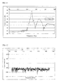
- FIG. 7 is a graph that shows all results obtained from measuring frequency characteristics of outputs Output 1, Output2, Output3 and Output4 with respect to an input in four SAW unit sensors S 1, S2, S3 and S4 according to First Experimental Example;
- FIG. 8 is a graph that shows results of measuring frequency of Output1 of the sensor S1, with respect to an input in the First Experimental Example.
- FIG. 9 is a graph that shows results of measuring frequency of Output2 of the sensor S2, with respect to an input in the First Experimental Example.
- FIG. 10 is a graph that shows a result of measuring frequency of Output3 of the sensor S3, with respect to an input in the First Experimental Example.
- FIG. 11 is a graph that shows a result of measuring frequency of Output4 of the sensor S4, with respect to an input in the First Experimental Example.
- FIG. 12 is a graph that shows a result of measuring interference between output IDTs of diagonal unit sensors S2 and S3 in Second Experimental Example;
- FIG. 13 is a graph that shows a result of measuring interference between output IDTs of opposite unit sensors S2 and S4 in the Second Experimental Example;
- FIG. 14 is a graph that shows a result of measuring interference between output IDTs of adjacent unit sensors S3 and S4 in the Second Experimental Example;
- FIG. 15 is a cross-sectional view of a SAW biosensor according to Third Experimental Example
- FIG. 16 is a graph that that depicts a result of measuring frequency characteristics between an input and an output on the basis of a reaction between a receptor and a target material in four unit sensors S1, S2, S3 and S4 in Third Experimental Example;
- FIG. 17 is a graph showing an amount of reduction in frequency according to concentration on the basis of a reference sensor. This result was obtained from the Third Experimental Example;
- FIG. 18 is a top view of a schematic diagram of an exemplary device that comprises a plurality of SAW devices
- FIG. 19 is a side view of the device of the FIG. 18 ;
- FIG. 20 is a side view of a schematic diagram of another exemplary device that comprises a plurality of SAW devices.
- first, second, third etc. may be used herein to describe various elements, components, regions, layers and/or sections, these elements, components, regions, layers and/or sections should not be limited by these terms. These terms are only used to distinguish one element, component, region, layer or section from another element, component, region, layer or section. Thus, a first element, component, region, layer or section discussed below could be termed a second element, component, region, layer or section without departing from the teachings of the invention.
- relative terms such as “lower” or “bottom” and “upper” or “top,” may be used herein to describe one element's relationship to another element as illustrated in the figures. It will be understood that relative terms are intended to encompass different orientations of the device in addition to the orientation depicted in the figures. For example, if the device in one of the figures is turned over, elements described as being on the “lower” side of other elements would then be oriented on “upper” sides of the other elements. The exemplary term “lower,” can therefore, encompasses both an orientation of “lower” and “upper,” depending on the particular orientation of the figure.
- Embodiments are described herein with reference to cross section illustrations that are schematic illustrations of idealized embodiments. As such, variations from the shapes of the illustrations as a result, for example, of manufacturing techniques and/or tolerances, are to be expected. Thus, embodiments described herein should not be construed as limited to the particular shapes of regions as illustrated herein, but are to include deviations in shapes that result, for example, from manufacturing. For example, a region illustrated or described as flat may, typically, have rough and/or nonlinear portions. Moreover, sharp angles that are illustrated may be rounded. Thus, the regions illustrated in the figures are schematic in nature and their shapes are not intended to illustrate the precise shape of a region and are not intended to limit the scope of the claims.
- a “surface acoustic wave” used herein may be abbreviated to "SAW”.
- the term “surface acoustic wave device” or “SAW device” may be understood to include all of a SAW filter, a SAW sensor, a SAW resonator, or a combination comprising at least one of the foregoing SAW devices. Further, the same reference numerals used throughout the different drawings to designate the same elements may be omitted.
- FIG. 1 schematically illustrates an exemplary embodiment of a SAW device.
- the SAW device 100 includes a substrate 110, an input inter-digital transducer ("IDT") 121 disposed on the substrate 110, output IDTs 131a, 132a, 133a and 134a disposed corresponding to the input IDT 121, and delay lines 141a, 142a, 143a and 144a interposed between the input IDT 121 and the output IDTs 131a, 132a, 133a and 134a.
- An interdigital transducer (IDT), or interdigitated transducer is a device which consists of two interlocking comb-shaped metallic coatings that is disposed on the substrate 110.
- the substrate 110 includes a piezoelectric material.
- the piezoelectric material has an electrical characteristic that is changed when a mechanical signal is applied (i.e., the piezoelectric effect). Conversely, a mechanical signal is generated when an electrical signal is applied (i.e., the reverse piezoelectric effect).
- the substrate may include piezoelectric materials which are dielectrics and comprise mainly metal oxides.
- the metal oxides may include, for example, but is not limited to, lithium niobate ("LiNbO 3 "), lithium tantalate (“LiTaO 3 "), lithium tetraborate ("Li 2 B 4 O 7 “), barium titanate (“BaTiO 3 "), lead zirconate (“PbZrO 3 “), lead titanate (“PbTiO 3 “), lead zirconate titanate (“PZT”), zinc oxide (“ZnO”), gallium arsenide (“GaAs”), quartz and niobate, berlinite, topaz, tourmaline group materials, potassium niobate, lithium niobate, sodium tungstate, Ba 2 NaNb 5 O 5 , Pb 2 KNb 5 O 15 , or the like, or a combination comprising at least one of the foregoing piezoelectric materials.
- the substrate may comprise piezoelectric polymers or copolymers or blends comprising at least one piezoelectric polymer.
- a suitable example of a piezoelectric polymer is polyvinylidene fluoride.
- Blends and copolymers of the polyvinylidene fluoride can also be used in the substrate.
- the copolymers can include block copolymers, alternating block copolymers, random copolymers, random block copolymers, graft copolymers, star block copolymers, or the like, or a combination comprising at least one of the foregoing thermoplastic polymers.
- suitable polymers that can be copolymerized with polyvinylidene fluoride are polytrifluoroethylene, polytetrafluoroethylene, polyacrylamide, polyhexafluoropropylene, polyacrylic acid, poly-(N-isopropylacrylamide), polyacetals, polyolefins, polyacrylics, polycarbonates, polystyrenes, polyesters, polyamides, polyamideimides, polyarylates, polyarylsulfones, polyethersulfones, polyphenylene sulfides, polyvinyl chlorides, polysulfones, polyimides, polyetherimides, polytetrafluoroethylenes, polyetherketones, polyether etherketones, polyether ketone ketones, polybenzoxazoles, polyphthalides, polyacetals, polyanhydrides, polyvinyl ethers, polyvinyl thioethers, polyvinyl alcohols, polyvinyl ketones, polyviny
- the piezoelectric material may included a composite that comprises a polymer blended with other piezoelectric polymers.
- the piezoelectric polymer may comprise other fillers that display piezoelectric properties to form a piezoelectric composition.
- these piezoelectric fillers are lithium niobate ("LiNbO 3 "), lithium tantalate (“LiTaO 3 "), lithium tetraborate (“Li 2 B 4 O 7 "), barium titanate (“BaTiO 3 "), lead zirconate (“PbZrO 3 "), lead titanate (“PbTiO 3 "), lead zirconate titanate (“PZT”), zinc oxide (“ZnO”), gallium arsenide (“GaAs”), quartz and niobate, berlinite, topaz, tourmaline group materials, potassium niobate, lithium niobate, sodium tungstate, Ba 2 NaNb 5 O 5 , Pb 2 KNb 5 O 15 , or
- piezoelectric fillers When piezoelectric fillers are added to the piezoelectric polymer to form the piezoelectric material, they can be added in amounts of up to about 50 weight percent (wt%), or in amounts of about 0.001 to about 5 wt%, or in amounts of about 0.01 to about 1 wt%, based on the total weight of the piezoelectric composition.
- the delay lines 141a, 142a, 143a and 144a are reaction areas at which target materials may be bound to a receptor and immobilized for sensing the target materials. Depending on the number of the delay lines, the number of target materials that can be sensed by the SAW device 100 may be determined. In the exemplary embodiment, the four delay lines 141a, 142a, 143a and 144a are disposed, thus three or four target materials, which are different from each other, may be sensed at the same time or sequentially.
- the number of delay lines can be from about 2 to about 12, or about 4 to about 10, or about 6 to about 8. In one embodiment, the number of delay lines can be from about 4 to about 6.
- These delay lines or reaction areas/sections 141a, 142a, 143a and 144a may include receptors specifically reacting (or interacting) with the target materials.
- the receptor may include a gas adsorbent, an enzyme, a microbe, an antibody, a deoxyribonucleic acid (DNA), a protein, a glycoprotein, a cytokine, a mixture of proteins, or a combination comprising at least one of the foregoing proteins.
- the reaction section may have a shape of a membrane or a cell that immobilizes the receptor.
- the input IDT 121 and the output IDTs 131a, 132a, 133a and 134a are disposed opposite one another.
- the input IDT 121 generates a surface acoustic wave by an applied first electrical signal. Therefore, the input IDT 121 may be referred to as a "transmitter.”
- the surface acoustic wave generated may be transmitted along the surface of the substrate 110 to the output IDTs 131a, 132a, 133a and 134a through expansion and compression at a selected frequency, and then converted into a second electrical signal by the reverse piezoelectric effect.
- These output IDTs 131a, 132a, 133a and 134a may be referred to as "receivers.”
- the transmitter and the receivers may be disposed on a surface of the same substrate 110 (as shown in FIG. 1 ).
- each IDT electrode includes two bar-shaped electrodes 401, and a plurality of fingers 402 that extend horizontally from each bar-shaped electrode.
- the fingers 402 extending from one of the bar-shaped electrodes 401 may alternate with those extending from the other bar-shaped electrode.
- Connection electrodes 403 may be electrically connected to the bar-shaped electrodes 401.
- the IDT electrode may include, but is not limited to, a thin-film metal, an electrically conducting ceramic or an electrically conducting plastic.
- thin-film metals are an aluminum alloy, a copper alloy, or gold, or the like, or a combination comprising at least one of the foregoing metals.
- thin-film ceramics are indium tin oxide, indium zinc oxide, fluorine doped tin oxide (FTO), doped zinc oxide, or the like, or a combination comprising at least one of the foregoing metal oxides.
- thin-film electrically conducting polymers include intrinsically conducting polymers or electrically insulating polymers that are made electrically conducting by the addition of electrically conducting fillers.
- Examples of intrinsically conducting polymers are polyaniline, polypyrrole, polyacetylene, polythiophene, or the like, or a combination comprising at least one of the foregoing intrinsically conducting polymers.
- the thin-film electrically conducting polymer may be an electrically insulating polymer that is compounded with an electrically conducting filler.
- electrically conducting fillers are metal particles (e.g., metal whiskers, metal fibers, and the like), carbon nanotubes, carbon black, graphite, indium tin oxide particles and whiskers, or the like, or a combination comprising at least one of the foregoing electrically conducting fillers.
- a protective layer such as an anti-oxidation layer may be formed on the surface of the IDT electrode.
- the IDT electrode may include aluminum or an aluminum alloy, and an aluminum oxide thin film formed on the surface thereof as the anti-oxidation layer.
- the aluminum alloy may include Al as a main component, and at least one of Ti, Si, Cr, W, Fe, Ni, Co, Pb, Nb, Ta, Zn, and V.
- the aluminum oxide thin film may be an artificially or natively formed aluminum oxide.
- An insulation layer may be formed to insulate the IDT electrode.
- the insulation layer may be used as a waveguide layer when Love waves are produced, in addition to insulating the IDT electrode.
- the insulation layer or the waveguide layer may include at least one of a silicon oxide (SiO 2 ) layer, a silicon nitride (Si x N y ) layer, a zinc oxide (ZnO) layer, a parylene layer, a polymethyl methacrylate (PMMA) layer, or the like, or a combination thereof.
- Other electrically insulating polymers listed above, may also be used as the insulation layer.
- only the silicon oxide layer may be used, or both the zinc oxide layer and the silicon oxide layer may be used in such a manner that the zinc oxide layer is coated with the silicon oxide layer.
- the fingers of the IDT electrode may include a bidirectional type, a single-phase unidirectional transducer (SPUDT) type, a floating-electrode unidirectional transducer (FEUDT) type, a split type, a reflector type, or the like, and at least one type of the fingers may be used.
- SPUDT single-phase unidirectional transducer
- FUDT floating-electrode unidirectional transducer
- split type a reflector type, or the like, and at least one type of the fingers may be used.
- FIG. 2 schematically illustrates an exemplary embodiment of a conventional SAW device.
- the SAW device include unit structures 10a, 10b, 10c and 10d in which input IDTs 12a, 12b, 12c and 12d are disposed so as to correspond to output IDTs 13a, 13b, 13c and 13d respectively, i.e. a single-input single-output (SISO) structure.
- SISO single-input single-output
- the input IDTs 12a, 12b, 12c and 12d correspond to the number of arranged input-output IDT unit structures.
- This conventional device produces a significant amount of noise and crosstalk because of the numerous input IDTs 12a, 12b, 12c and 12d and the numerous output IDTs 13a, 13b, 13c and 13d all of which are clustered together in close proximity to each other.
- the SAW device includes the single input IDT 121 and the multiple output IDTs 131a, 132a, 133a and 134a, which are arranged in a single-input multi-output (SIMO) structure. Th at is, a plurality of the output IDTs 131a, 132a, 133a and 134a are arranged to be parallel to the longitudinal direction of the single input IDT 121. In one embodiment, the interdigitated fingers of the output IDTs are parallel to the interdigitated fingers of the input IDTs.
- the SAW device may be used as a sensor in that it has an arrangement structure for sensing two or more target materials.
- the arrangement shown in the FIG. 1 is capable of fundamentally interrupting the noise and interference that may be generated from the structure shown in the conventional SAW device of the FIG. 2 . This is because only as many IDT sites are utilized on the single IDT 121 as the number of desired detection targets.
- the sensor itself is downsized (i.e., reduced in size), so that the SAW device advantageously increases yield, and reduces the quantity of samples used for sensing.
- the four output IDTs 131a, 132a, 133a and 134a are arranged in a row in the longitudinal direction of the single input IDT 121.
- the number of output IDTs may be two or more within the limited length of the finger of the input IDT 121.
- a maximum value of the length W in of the finger (e.g., a single finger) of the input IDT is determined by the IL of the input IDT.
- the IL value can be various numbers and determined based on a final application of the device.
- the length W in of the finger of the input IDT is regarded as the maximum length (represented by the multiple of a wavelength).
- FIG 3 is a graph that shows a result of simulating the IL of an input IDT, when the input and output IDTs are disposed such that one wavelength (1 ⁇ ) is 20 micrometers (" ⁇ m").
- the IL decreases.
- the length W in of the finger of the input IDT in the sensor is proportional to an area of the sensing layer corresponding to the delay lines, if the length W in of the finger of the input IDT decreases, the sensed area also decreases.
- the maximum value of the length W in of the fingers of the input IDT depends on the allowable IL. When - 30 dB is generally regarded as a maximum loss of the sensor, the maximum value of the length W in may be about 300 ⁇ , where ⁇ is the wavelength of the surface acoustic wave.
- a minimum value of the length W in of the finger of the input IDT is about 80 ⁇ to 100 ⁇ because at least two output IDTs are arranged in a transverse direction.
- output IDTs 131a, 132a, 133a and 134a; and 131b, 132b, 133b and 134b may be disposed on upper and lower sides of the single input IDT 121, respectively (see FIG. 4 ).
- the output IDTs have the maximum number m max when the length W in of the finger of the input IDT is the maximum value and when the length W out of the finger of the output IDT is the minimum value.
- the minimum length W out of the finger of the output IDT is set to 50 ⁇ .
- the minimum length W out may be properly set according to the device, and is therefore not limited.
- two or more of the output IDTs 131a, 132a, 133a and 134a may be disposed on a substrate per single input IDT 121.
- the four output IDTs 131a, 132a, 133a and 134a are disposed in a row in the longitudinal direction of the input IDT 121.
- two or more output IDTs can be disposed parallel to the input IDT.
- another exemplary embodiment of the SAW device 101 may include first output IDTs 131a, 132a, 133a and 134a and second output IDTs 131b, 132b, 133b and 134b, which are disposed on an opposite sides of the input IDT 121 from the side on which the first output IDTs 131a, 132a, 133a and 134a are disposed.
- the sets of first output IDTs and second output IDTs are disposed to lie parallel to each other in the longitudinal direction of the input IDT 121.
- the first output IDTs 131a, 132a, 133a and 134a and the second output IDTs 131b, 132b, 133b and 134b are disposed so as to correspond to each other in a transverse direction (perpendicular to the longitudinal direction) with the input IDT 121 interposed therebetween.
- the design is not limited to the input IDT 121 being opposite to the output IDTs 131b, 132b, 133b and 134b with delay lines 141b, 142b, 143b and 144b interposed therebetween.
- an alternative exemplary embodiment of the SAW device 102 may include first output IDTs 131a, 132a and 133a and second output IDTs 131b, 132b, 133b and 134b, which are disposed in a zigzag form with the input IDT 121 interposed therebetween.
- the exemplary embodiments of the SAW devices 100, 101 and 102 may include a sensor for sensing a target material.
- a driving principle of the SAW sensor 100 will be described with reference to FIGS. 1 and 15 .
- An electrical signal generates a mechanical wave while passing through the IDT electrode 121. This wave is changed via physical, chemical and electrical interactions, when the target material 220 in the sample binds to the receptor 210 on the surface of the SAW sensor 100. That is, a central frequency, phase, or signal intensity of the output signal of the SAW sensor is changed when the target material binds to (reacts with) the receptor 210 on the surface of the SAW sensor 100.
- the target material 220 when the weight of the receptor is changed by the binding of the target material 220, the shear velocity of the SAW excited by the input IDT 121 is changed, and the oscillation frequency of the output IDT 131 receiving the SAW of the changed shear velocity is changed. Accordingly, physical properties of the target materials 220 may be precisely detected by measuring the change of the oscillation frequency. In addition, the target material 220 may be qualitatively and quantitatively analyzed.
- the SAW generically refers to waves, which concentrate and transmit energy on the vicinity of the surface of a medium.
- the SAW can be excited and received by the IDT electrodes 121 and 131 disposed on the surface of the piezoelectric substrate 110.
- the SAWs used for the SAW device may include a shear horizontal (SH) wave, a Love wave, a leaky surface acoustic wave, and the like, in addition to the well known Rayleigh wave.
- An exemplary embodiment of the SAW device may use the Love wave.
- a mode of the Love wave generally has an effective coupling coefficient and a low loss, compared to that of the leaky wave, such as the Rayleigh wave or the SH wave.
- a surface layer 300 may include a high-density dielectric layer or polymer layer, in which the speed of sound is slow so as to form a waveguide path on the piezoelectric substrate 110.
- the Love wave reduces the speed of a surface wave, and makes the speed of the surface wave slower than that of a slow transverse wave. Therefore, the Love wave is known as the surface wave, which concentrates the energy of a bulk wave having only a transverse wave on the vicinity of the surface of the substrate 110.
- the SAW device may be constructed so as to make multiple measurements rapidly for purposes of affecting a combinatorial method of measuring sample properties.
- An exemplary device of this nature is depicted in the FIG.s. 18 to 20 which will be discussed in detail below.
- the high-density dielectric layer may include a metal oxide layer or a polymeric layer.
- the high-density dielectric layer may include, but is not limited to, tantalum pentoxide (Ta 2 O 5 ), zinc oxide (ZnO), sapphire (Al 2 O 3 ), titanium dioxide (rutile) (TiO 2 ), niobium pentoxide (Nb 2 O 5 ), bismuth germanium oxide (Bi 12 GeO 20 ; BGO), bismuth trioxide (Bi 2 O 3 ), or the like, or a combination comprising at least one of the foregoing metal oxides.
- the polymer layer may include, but is not limited to, parylene, polymethyl methacrylate (PMMA), benzocyclobutene (BCB), polyolefins, polycarbonates, polystyrenes, polyesters, polyamides, polyamideimides, polyarylates, polyarylsulfones, polyethersulfones, polyphenylene sulfides, polysulfones, polyimides, polyetherimides, or the like, or a combination comprising at least one of the foregoing polymers.
- PMMA polymethyl methacrylate
- BCB benzocyclobutene
- polyolefins polycarbonates
- polystyrenes polyesters
- polyamides polyamideimides
- polyarylates polyarylates
- polyarylsulfones polyethersulfones
- polyphenylene sulfides polysulfones
- polyimides polyetherimides, or the like, or a combination comprising at least
- the SAW sensor may be applied to an oscillation method, and may further include an external resonator (not shown).
- the resonator is a circuit for generating a sinusoidal signal of a certain frequency, and converts DC energy into AC energy. Frequency signals within a narrow band may be detected by only an output port without an input port.
- This SAW sensor may analyze physical properties such as mass, pressure, density, viscosity, or the like, of the target material. Further, the SAW sensor described herein may obtain a greater change in frequency than a comparative sensor, and may be used to determine characteristics of a sample in a liquid phase or in a gas phase. The SAW sensor has at least ten times, or at least fifteen times, or at least twenty times, a greater excited frequency, compared with that of an existing comparative biosensor.
- the SAW sensor may be fabricated in a small size due to ease of integration and manufacturing, be measured in real time, and reduce the sample size that needs to be used for a measurement. Accordingly, the SAW sensor may used as a biosensor for detecting physical properties or characteristics of the target material to be biologically detected.
- the biosensor may be used to detect characteristics and properties of biological materials such as enzymes, fungi, proteins, nucleic acids and other biological tissues.
- the device may include a plurality of SAW devices to conduct rapid testing on a large number of samples.
- a plurality of SAW devices 101 may be disposed upon a rotary table or platform.
- a plurality of SAW devices 101A, 101B, 101C and 101D are disposed upon a rotary platform 304. While the FIG. 18 shows only four SAW devices 101A, 101B, 101C and 101D disposed upon the rotary platform 304, fewer or larger numbers of the SAW devices may be disposed upon the rotary platform 304.
- the rotary platform 304 rotates about a vertical axis disposed in the vertical support 302.
- the vertical support 302 is disposed upon a base plate 306 as shown in FIG. 19 .
- FIG. 20 depicts another embodiment, of such a device 300'.
- the individual SAW devices 101A', 101B', 101C' and 101D' are disposed upon rotary arms 308 that rotate about a horizontally disposed shaft 310.
- the horizontal shaft 310 is supported on a vertical support 302' (or a pair of vertical supports if desired) that is disposed upon a base plate 306'.
- the devices depicted in the FIGs. 18 , 19 and 20 can be used for rapid testing of a large number of samples. They can be advantageously used for combinatorial testing of samples.
- the rotary platform 304 and the rotary arms 308 may be manufactured from a dielectric material. Examples of dielectric materials are provided above.
- a method of manufacturing a surface acoustic wave device comprises disposing a single input inter-digital transducer on a piezoelectric substrate, the input inter-digital transducer converting a first electrical signal into a surface acoustic wave signal; disposing a plurality of output inter-digital transducers on the piezoelectric substrate, the output inter-digital transducers converting the surface acoustic wave signal into a second electrical signal; and disposing a delay line between the input inter-digital transducer and the output inter-digital transducers, wherein the plurality of the output inter-digital transducers are arranged in a longitudinal direction of the input inter-digital transducer.
- a method of manufacturing the surface acoustic wave device comprises disposing upon a substrate a transmitter where the transmitter is operative to generate a surface acoustic wave. At least two receivers are disposed on the substrate, the receivers converting the received surface acoustic wave into an electrical signal to receive the surface acoustic wave. A receptor that reacts/interacts with the target material is immobilized between the transmitter and the receivers. The generated surface acoustic wave is dependent upon the receptor-target material combination. Thus the target material is detected.
- the method may further comprise disposing a plurality of surface wave acoustic devices on a surface that rotates; the surface rotating about a vertical axis or a horizontal axis.
- the target material 220 may include biomolecules such as proteins, antibodies, antigens, DNA, RNA, bacteria, animal cells, viruses, tissues or the like, or biological solutions such as toxins produced thereby.
- the receptor 210 which specifically binds to the target material 220 may include proteins, antibodies, antigens, enzymes, DNA, RNA, peptide nucleic acid (PNA) (artificial DNA), cells, olfactory nerves, or the like.
- PNA peptide nucleic acid
- a disease may be checked by using the SAW biosensor in which the receptors 210 are those that specifically react to a certain bacteria that cause the disease.
- the SAW sensor may be used to check the disease depending on whether a specimen obtained from a patient reacts with the receptors 210 of the SAW sensor.
- the SAW device may include a plurality of SAW unit sensors, thus a variety of tests may be performed by using a small quantity of sample in a quick and efficient manner.
- the size of a substrate is 8 mm X 10 mm
- the length W in of the finger of the input IDT is 200 ⁇ (where 1 ⁇ is 20 ⁇ m)
- the number of fingers for the input IDT is 50 (in FIG. 6 , only six fingers are symbolically shown in each IDT).
- the length W out of the finger of the output IDT is 80 ⁇
- the number of fingers of each output IDT is 50.
- the IDTs are formed by the deposition of aluminum (Al), wherein two output IDTs are disposed on each side of the input IDT, and thus a total of four output IDTs are disposed for the single input IDT.
- An interval between the output IDTs is set to 40 ⁇ , and the length of the delay line between the input IDT and the output IDT is set to 100 ⁇ .
- one unit sensor includes one output IDT, one input IDT, and one delay line.
- the device of the Figure 6 displays four unit sensors S1, S2, S3 and S4.
- the reducible portions may include a portion where a pad for an electrode can be connected with an electric circuit at the adjacent output IDTs, the distance between the input IDT and an edge of the sensor, the distance between the output IDT and the sensor edge, the length W out of the finger of the output IDT, and so on.
- FIGS. 7 to 11 Frequencies measured from the four output IDTs of the four unit sensors S1, S2, S3 and S4 are shown in FIGS. 7 to 11 , respectively.
- Figure 7 shows all of the outputs from the four unit sensors S1, S2, S3 and S4 on a single plot, while the Figures 8 through 11 show the outputs of the individual sensors S1, S2, S3 and S4 respectively. As may be in these figures, it is found that the four output signals are substantially similar to each other.
- the interference between the output IDTs is checked by measuring the level of power between the output IDTs with a network analyzer (available from Agilent, 8753ES).
- the power level is less than -80 dB, and there is no measurement error caused as a result of interference between the diagonal output IDTs S2 and S3.
- the maximum power level is less than -30 dB, which is higher than that between the diagonal output IDTs, and as a result, no interference exists between S2 and S4 because no peak point is generated from a signal form, compared with normal input and output characteristics.
- protein A a receptor is immobilized to the surface of the sensor at different concentrations, and then a first central frequency is measured from the input and output IDTs.
- the target proteins IgG to be sensed are reacted with the receptor, and then a second central frequency is measured. A difference between the measured first and second central frequencies is checked, and the result is shown in FIG. 16 .
- S1 is used as a reference sensor.
- a phosphate buffered saline (PBS) buffer is mixed with the receptor for the reference sensor, while samples containing different proteins IgG are mixed with the receptor and then the target proteins may react with the receptor for the other three sensors S2, S3 and S4.
- a change in frequency is witnessed at each concentration, because of the increase in mass at each of the other three sensors S2, S3 and S4.
- S1 is the reference sensor, and the reaction is performed when the concentrations of the proteins IgG to be sensed for S2 to S4 are 0.1 mg/mL, 0.5 mg/mL, and 1 mg/mL respectively. It is found from this result that as the concentration increases, i.e., the mass increases, the reduction in the frequency increases.
- the amount of the reduction in the frequency at each concentration on the basis of the reference sensor is shown in Table 1 below as well as in the FIG. 17 .
Landscapes
- Physics & Mathematics (AREA)
- Acoustics & Sound (AREA)
- General Health & Medical Sciences (AREA)
- Chemical & Material Sciences (AREA)
- Analytical Chemistry (AREA)
- Biochemistry (AREA)
- Life Sciences & Earth Sciences (AREA)
- General Physics & Mathematics (AREA)
- Immunology (AREA)
- Pathology (AREA)
- Health & Medical Sciences (AREA)
- Investigating Or Analyzing Materials By The Use Of Ultrasonic Waves (AREA)
- Surface Acoustic Wave Elements And Circuit Networks Thereof (AREA)
Applications Claiming Priority (1)
| Application Number | Priority Date | Filing Date | Title |
|---|---|---|---|
| KR1020100106534A KR101711204B1 (ko) | 2010-10-29 | 2010-10-29 | 단일입력 다중출력 표면탄성파 디바이스 |
Publications (3)
| Publication Number | Publication Date |
|---|---|
| EP2447713A2 true EP2447713A2 (de) | 2012-05-02 |
| EP2447713A3 EP2447713A3 (de) | 2013-04-24 |
| EP2447713B1 EP2447713B1 (de) | 2017-11-08 |
Family
ID=44759475
Family Applications (1)
| Application Number | Title | Priority Date | Filing Date |
|---|---|---|---|
| EP11181086.7A Not-in-force EP2447713B1 (de) | 2010-10-29 | 2011-09-13 | Oberflächenwellenbauelement mit einem Eingang und mehreren Ausgängen |
Country Status (3)
| Country | Link |
|---|---|
| US (1) | US8695428B2 (de) |
| EP (1) | EP2447713B1 (de) |
| KR (1) | KR101711204B1 (de) |
Cited By (3)
| Publication number | Priority date | Publication date | Assignee | Title |
|---|---|---|---|---|
| CN103490135A (zh) * | 2013-09-12 | 2014-01-01 | 电子科技大学 | Ltcc延迟线组件 |
| CN108896665A (zh) * | 2018-08-27 | 2018-11-27 | 国网山东省电力公司电力科学研究院 | 工作场所防噪耳塞的适用性评估方法 |
| CN116315533A (zh) * | 2023-02-08 | 2023-06-23 | 西安交通大学 | 一种谐振器及紧凑型极窄带高温超导滤波器 |
Families Citing this family (7)
| Publication number | Priority date | Publication date | Assignee | Title |
|---|---|---|---|---|
| EP2557420B1 (de) * | 2011-08-12 | 2015-10-14 | Nxp B.V. | Halbleitervorrichtung mit Au-Cu-Elektroden und Verfahren zur Herstellung der Halbleitervorrichtung |
| US9647637B2 (en) * | 2012-06-05 | 2017-05-09 | Snaptrack, Inc. | Saw filter with improved stop band suppression |
| KR101911437B1 (ko) | 2012-06-27 | 2018-10-24 | 삼성전자주식회사 | Saw 배열 센서 |
| US9726646B1 (en) * | 2013-05-29 | 2017-08-08 | National Technology & Engineering Solutions Of Sandia, Llc | Resonant surface acoustic wave chemical detector |
| WO2017151869A1 (en) * | 2016-03-02 | 2017-09-08 | Cornell University | Surface acoustic wave (saw)-based inertial sensor, methods, and applications |
| JP6680358B2 (ja) * | 2016-06-28 | 2020-04-15 | 株式会社村田製作所 | 弾性波装置 |
| DE102023119113B3 (de) | 2023-07-19 | 2024-10-31 | Leibniz-Institut für Festkörper- und Werkstoffforschung Dresden e.V. (IFW Dresden e.V.) | Modulare Vorrichtung zur Bestimmung von richtungsabhängigen Eigenschaften von Schichten und Schichtsystemen |
Citations (1)
| Publication number | Priority date | Publication date | Assignee | Title |
|---|---|---|---|---|
| KR20100106534A (ko) | 2007-12-24 | 2010-10-01 | 콸콤 인코포레이티드 | 통신 장치 상에서 콘텐츠를 검색/다운로딩하기 위한 장치 및 방법들 |
Family Cites Families (29)
| Publication number | Priority date | Publication date | Assignee | Title |
|---|---|---|---|---|
| US3479572A (en) * | 1967-07-06 | 1969-11-18 | Litton Precision Prod Inc | Acoustic surface wave device |
| US3898592A (en) * | 1974-05-08 | 1975-08-05 | Sperry Rand Corp | Acoustic surface wave signal processors |
| GB2029148A (en) * | 1978-07-12 | 1980-03-12 | Gen Electric Co Ltd | Surface wave devices |
| US4926146A (en) * | 1988-05-09 | 1990-05-15 | Trw Inc. | Parallel-to-serial signal processor using surface acoustic waves |
| JP2847438B2 (ja) * | 1991-03-29 | 1999-01-20 | 三井金属鉱業株式会社 | 弾性表面波素子 |
| GB2310776B (en) * | 1995-07-10 | 1998-07-08 | Matsushita Electric Industrial Co Ltd | Spread spectrum communication apparatus and demodulator surface acoustic wave element and surface acoustic wave parts for spread spectrum communication |
| JP3424453B2 (ja) * | 1996-08-09 | 2003-07-07 | 松下電器産業株式会社 | スペクトラム拡散通信装置 |
| CA2398713A1 (en) * | 2000-02-02 | 2001-08-09 | Rutgers, The State University Of New Jersey | Programmable surface acoustic wave (saw) filter |
| TW483238B (en) * | 2000-06-30 | 2002-04-11 | Fujitsu Media Devices Ltd | Surface acoustic wave device |
| US6534896B2 (en) * | 2001-05-15 | 2003-03-18 | Nortel Networks Limited | Spatial harmonic transducers for surface wave devices |
| BR0212721A (pt) * | 2001-10-16 | 2004-10-05 | Transense Technologies Plc | Sensor de saw de temperatura estável com constantes eláticas de terceira ordem |
| US7047792B1 (en) * | 2003-07-07 | 2006-05-23 | University Of South Florida | Surface acoustic wave hydrogen sensor |
| US7053523B1 (en) * | 2004-02-02 | 2006-05-30 | The United States Of America As Represented By The Secretary Of The Army | Lateral field excitation of bulk acoustic waves from an IC-compliant low voltage source |
| US7888842B2 (en) * | 2004-02-13 | 2011-02-15 | University Of Maine System Board Of Trustees | Ultra-thin film electrodes and protective layer for high temperature device applications |
| US7134319B2 (en) * | 2004-08-12 | 2006-11-14 | Honeywell International Inc. | Acoustic wave sensor with reduced condensation and recovery time |
| JP2006123715A (ja) | 2004-10-28 | 2006-05-18 | Nhk Spring Co Ltd | 車両用シート |
| JP4714885B2 (ja) * | 2005-03-18 | 2011-06-29 | 日本無線株式会社 | 弾性波センサ |
| WO2006114829A1 (ja) | 2005-04-06 | 2006-11-02 | Murata Manufacturing Co., Ltd. | 表面波センサ装置 |
| US8143681B2 (en) * | 2006-04-20 | 2012-03-27 | The George Washington University | Saw devices, processes for making them, and methods of use |
| TWI331216B (en) | 2006-06-15 | 2010-10-01 | Murata Manufacturing Co | Sensor for detecting substance in liquid |
| US20080084135A1 (en) * | 2006-10-10 | 2008-04-10 | Honeywell International Inc. | Universal platform for surface acoustic wave (SAW) based sensors |
| US20090124513A1 (en) | 2007-04-20 | 2009-05-14 | Patricia Berg | Multiplex Biosensor |
| US7855564B2 (en) * | 2008-02-14 | 2010-12-21 | Delaware Capital Formation, Inc. | Acoustic wave device physical parameter sensor |
| US7695993B2 (en) * | 2008-05-07 | 2010-04-13 | Honeywell International Inc. | Matrix nanocomposite sensing film for SAW/BAW based hydrogen sulphide sensor and method for making same |
| US20100058834A1 (en) * | 2008-09-09 | 2010-03-11 | Honeywell International Inc. | Method and apparatus for low drift chemical sensor array |
| KR101529169B1 (ko) * | 2009-06-11 | 2015-06-16 | 삼성전자주식회사 | Saw 센서 디바이스 |
| KR101655302B1 (ko) * | 2009-09-22 | 2016-09-07 | 삼성전자주식회사 | 표면 탄성파 센서 시스템 |
| KR101638811B1 (ko) * | 2009-11-06 | 2016-07-12 | 삼성전자주식회사 | 발진 방식을 이용한 표면탄성파 센서 시스템 및 이를 이용한 검출방법 |
| US20110236877A1 (en) * | 2010-03-26 | 2011-09-29 | Da-Jeng Yao | Biosensor and method using the same to perform a biotest |
-
2010
- 2010-10-29 KR KR1020100106534A patent/KR101711204B1/ko not_active Expired - Fee Related
-
2011
- 2011-06-29 US US13/172,431 patent/US8695428B2/en not_active Expired - Fee Related
- 2011-09-13 EP EP11181086.7A patent/EP2447713B1/de not_active Not-in-force
Patent Citations (1)
| Publication number | Priority date | Publication date | Assignee | Title |
|---|---|---|---|---|
| KR20100106534A (ko) | 2007-12-24 | 2010-10-01 | 콸콤 인코포레이티드 | 통신 장치 상에서 콘텐츠를 검색/다운로딩하기 위한 장치 및 방법들 |
Cited By (4)
| Publication number | Priority date | Publication date | Assignee | Title |
|---|---|---|---|---|
| CN103490135A (zh) * | 2013-09-12 | 2014-01-01 | 电子科技大学 | Ltcc延迟线组件 |
| CN103490135B (zh) * | 2013-09-12 | 2015-07-15 | 电子科技大学 | Ltcc延迟线组件 |
| CN108896665A (zh) * | 2018-08-27 | 2018-11-27 | 国网山东省电力公司电力科学研究院 | 工作场所防噪耳塞的适用性评估方法 |
| CN116315533A (zh) * | 2023-02-08 | 2023-06-23 | 西安交通大学 | 一种谐振器及紧凑型极窄带高温超导滤波器 |
Also Published As
| Publication number | Publication date |
|---|---|
| EP2447713B1 (de) | 2017-11-08 |
| KR101711204B1 (ko) | 2017-03-13 |
| EP2447713A3 (de) | 2013-04-24 |
| US8695428B2 (en) | 2014-04-15 |
| KR20120045167A (ko) | 2012-05-09 |
| US20120105174A1 (en) | 2012-05-03 |
Similar Documents
| Publication | Publication Date | Title |
|---|---|---|
| EP2447713B1 (de) | Oberflächenwellenbauelement mit einem Eingang und mehreren Ausgängen | |
| EP2543996B1 (de) | Oberflächenwellen-Sensorsystem und Messverfahren mithilfe einer Mehrfachtransitechowelle | |
| US8742645B2 (en) | Surface acoustic wave sensor system | |
| US8436509B1 (en) | High-frequency shear-horizontal surface acoustic wave sensor | |
| US5130257A (en) | Chemical sensor utilizing a surface transverse wave device | |
| WO2011030519A1 (ja) | 弾性波素子と弾性波素子センサ | |
| US20060254356A1 (en) | Wireless and passive acoustic wave liquid conductivity sensor | |
| US20130130362A1 (en) | Power spectral density chemical and biological sensor | |
| US7936106B2 (en) | Surface acoustic wave sensor device | |
| US7771987B2 (en) | Acoustic wave sensor assembly utilizing a multi-element structure | |
| JP2006313092A (ja) | 弾性表面波センサ及び弾性表面波センサシステム | |
| US9128033B2 (en) | Multiple surface acoustic wave sensor system | |
| Sherrit et al. | BAW and SAW sensors for in situ analysis | |
| US20110111516A1 (en) | Surface acoustic wave sensor system for using oscillation method and sensing method using the same | |
| Da Cunha et al. | LGX pure shear horizontal SAW for liquid sensor applications | |
| WO2008019694A2 (en) | Bio surface acoustic wave (saw) resonator design for detection of a target analyte | |
| US20130139599A1 (en) | Apparatus and method for measuring signal using sinc function | |
| Kustanovich et al. | Design and characterization of surface acoustic wave resonance (SAR) system for in-liquid sensing | |
| Schweyer et al. | Comparison of surface transverse wave (STW) and shear horizontal acoustic plate mode (SHAPM) devices for biochemical sensors | |
| Rashid et al. | Surface Acoustic Wave Sensors | |
| JP4504106B2 (ja) | 表面弾性波素子による測定方法 | |
| JP2005315646A (ja) | 弾性表面波センサ及び弾性表面波センサシステム | |
| Taha et al. | On the analysis of the interaction between surface acoustic wave (SAW) and adjacent media | |
| Andle et al. | Application of unidirectional transducers in acoustic plate mode biosensors | |
| Tomar et al. | Rayleigh Wave–Based Surface Acoustic Wave Devices: Importance and Applications |
Legal Events
| Date | Code | Title | Description |
|---|---|---|---|
| PUAI | Public reference made under article 153(3) epc to a published international application that has entered the european phase |
Free format text: ORIGINAL CODE: 0009012 |
|
| AK | Designated contracting states |
Kind code of ref document: A2 Designated state(s): AL AT BE BG CH CY CZ DE DK EE ES FI FR GB GR HR HU IE IS IT LI LT LU LV MC MK MT NL NO PL PT RO RS SE SI SK SM TR |
|
| AX | Request for extension of the european patent |
Extension state: BA ME |
|
| RAP1 | Party data changed (applicant data changed or rights of an application transferred) |
Owner name: AJOU UNIVERSITY INDUSTRY-ACADEMIC COOPERATION FOUN Owner name: SAMSUNG ELECTRONICS CO., LTD. |
|
| PUAL | Search report despatched |
Free format text: ORIGINAL CODE: 0009013 |
|
| AK | Designated contracting states |
Kind code of ref document: A3 Designated state(s): AL AT BE BG CH CY CZ DE DK EE ES FI FR GB GR HR HU IE IS IT LI LT LU LV MC MK MT NL NO PL PT RO RS SE SI SK SM TR |
|
| AX | Request for extension of the european patent |
Extension state: BA ME |
|
| RIC1 | Information provided on ipc code assigned before grant |
Ipc: H03H 9/00 20060101ALI20130319BHEP Ipc: G01N 29/02 20060101AFI20130319BHEP Ipc: G01N 29/036 20060101ALI20130319BHEP Ipc: H03H 9/64 20060101ALI20130319BHEP |
|
| 17P | Request for examination filed |
Effective date: 20131024 |
|
| RBV | Designated contracting states (corrected) |
Designated state(s): AL AT BE BG CH CY CZ DE DK EE ES FI FR GB GR HR HU IE IS IT LI LT LU LV MC MK MT NL NO PL PT RO RS SE SI SK SM TR |
|
| 17Q | First examination report despatched |
Effective date: 20160915 |
|
| RIN1 | Information on inventor provided before grant (corrected) |
Inventor name: LEE, YEOL HO Inventor name: LEE, SOO SUK Inventor name: LEE, KEE KEUN |
|
| GRAP | Despatch of communication of intention to grant a patent |
Free format text: ORIGINAL CODE: EPIDOSNIGR1 |
|
| INTG | Intention to grant announced |
Effective date: 20170530 |
|
| GRAS | Grant fee paid |
Free format text: ORIGINAL CODE: EPIDOSNIGR3 |
|
| GRAA | (expected) grant |
Free format text: ORIGINAL CODE: 0009210 |
|
| AK | Designated contracting states |
Kind code of ref document: B1 Designated state(s): AL AT BE BG CH CY CZ DE DK EE ES FI FR GB GR HR HU IE IS IT LI LT LU LV MC MK MT NL NO PL PT RO RS SE SI SK SM TR |
|
| REG | Reference to a national code |
Ref country code: GB Ref legal event code: FG4D |
|
| REG | Reference to a national code |
Ref country code: CH Ref legal event code: EP Ref country code: AT Ref legal event code: REF Ref document number: 944614 Country of ref document: AT Kind code of ref document: T Effective date: 20171115 |
|
| REG | Reference to a national code |
Ref country code: IE Ref legal event code: FG4D |
|
| REG | Reference to a national code |
Ref country code: DE Ref legal event code: R096 Ref document number: 602011043105 Country of ref document: DE |
|
| REG | Reference to a national code |
Ref country code: NL Ref legal event code: MP Effective date: 20171108 |
|
| REG | Reference to a national code |
Ref country code: LT Ref legal event code: MG4D |
|
| REG | Reference to a national code |
Ref country code: AT Ref legal event code: MK05 Ref document number: 944614 Country of ref document: AT Kind code of ref document: T Effective date: 20171108 |
|
| PG25 | Lapsed in a contracting state [announced via postgrant information from national office to epo] |
Ref country code: LT Free format text: LAPSE BECAUSE OF FAILURE TO SUBMIT A TRANSLATION OF THE DESCRIPTION OR TO PAY THE FEE WITHIN THE PRESCRIBED TIME-LIMIT Effective date: 20171108 Ref country code: NL Free format text: LAPSE BECAUSE OF FAILURE TO SUBMIT A TRANSLATION OF THE DESCRIPTION OR TO PAY THE FEE WITHIN THE PRESCRIBED TIME-LIMIT Effective date: 20171108 Ref country code: SE Free format text: LAPSE BECAUSE OF FAILURE TO SUBMIT A TRANSLATION OF THE DESCRIPTION OR TO PAY THE FEE WITHIN THE PRESCRIBED TIME-LIMIT Effective date: 20171108 Ref country code: FI Free format text: LAPSE BECAUSE OF FAILURE TO SUBMIT A TRANSLATION OF THE DESCRIPTION OR TO PAY THE FEE WITHIN THE PRESCRIBED TIME-LIMIT Effective date: 20171108 Ref country code: NO Free format text: LAPSE BECAUSE OF FAILURE TO SUBMIT A TRANSLATION OF THE DESCRIPTION OR TO PAY THE FEE WITHIN THE PRESCRIBED TIME-LIMIT Effective date: 20180208 Ref country code: ES Free format text: LAPSE BECAUSE OF FAILURE TO SUBMIT A TRANSLATION OF THE DESCRIPTION OR TO PAY THE FEE WITHIN THE PRESCRIBED TIME-LIMIT Effective date: 20171108 |
|
| PG25 | Lapsed in a contracting state [announced via postgrant information from national office to epo] |
Ref country code: GR Free format text: LAPSE BECAUSE OF FAILURE TO SUBMIT A TRANSLATION OF THE DESCRIPTION OR TO PAY THE FEE WITHIN THE PRESCRIBED TIME-LIMIT Effective date: 20180209 Ref country code: BG Free format text: LAPSE BECAUSE OF FAILURE TO SUBMIT A TRANSLATION OF THE DESCRIPTION OR TO PAY THE FEE WITHIN THE PRESCRIBED TIME-LIMIT Effective date: 20180208 Ref country code: IS Free format text: LAPSE BECAUSE OF FAILURE TO SUBMIT A TRANSLATION OF THE DESCRIPTION OR TO PAY THE FEE WITHIN THE PRESCRIBED TIME-LIMIT Effective date: 20180308 Ref country code: LV Free format text: LAPSE BECAUSE OF FAILURE TO SUBMIT A TRANSLATION OF THE DESCRIPTION OR TO PAY THE FEE WITHIN THE PRESCRIBED TIME-LIMIT Effective date: 20171108 Ref country code: AT Free format text: LAPSE BECAUSE OF FAILURE TO SUBMIT A TRANSLATION OF THE DESCRIPTION OR TO PAY THE FEE WITHIN THE PRESCRIBED TIME-LIMIT Effective date: 20171108 Ref country code: RS Free format text: LAPSE BECAUSE OF FAILURE TO SUBMIT A TRANSLATION OF THE DESCRIPTION OR TO PAY THE FEE WITHIN THE PRESCRIBED TIME-LIMIT Effective date: 20171108 Ref country code: HR Free format text: LAPSE BECAUSE OF FAILURE TO SUBMIT A TRANSLATION OF THE DESCRIPTION OR TO PAY THE FEE WITHIN THE PRESCRIBED TIME-LIMIT Effective date: 20171108 |
|
| PG25 | Lapsed in a contracting state [announced via postgrant information from national office to epo] |
Ref country code: CZ Free format text: LAPSE BECAUSE OF FAILURE TO SUBMIT A TRANSLATION OF THE DESCRIPTION OR TO PAY THE FEE WITHIN THE PRESCRIBED TIME-LIMIT Effective date: 20171108 Ref country code: EE Free format text: LAPSE BECAUSE OF FAILURE TO SUBMIT A TRANSLATION OF THE DESCRIPTION OR TO PAY THE FEE WITHIN THE PRESCRIBED TIME-LIMIT Effective date: 20171108 Ref country code: CY Free format text: LAPSE BECAUSE OF FAILURE TO SUBMIT A TRANSLATION OF THE DESCRIPTION OR TO PAY THE FEE WITHIN THE PRESCRIBED TIME-LIMIT Effective date: 20171108 Ref country code: SK Free format text: LAPSE BECAUSE OF FAILURE TO SUBMIT A TRANSLATION OF THE DESCRIPTION OR TO PAY THE FEE WITHIN THE PRESCRIBED TIME-LIMIT Effective date: 20171108 Ref country code: DK Free format text: LAPSE BECAUSE OF FAILURE TO SUBMIT A TRANSLATION OF THE DESCRIPTION OR TO PAY THE FEE WITHIN THE PRESCRIBED TIME-LIMIT Effective date: 20171108 |
|
| REG | Reference to a national code |
Ref country code: DE Ref legal event code: R097 Ref document number: 602011043105 Country of ref document: DE |
|
| REG | Reference to a national code |
Ref country code: FR Ref legal event code: PLFP Year of fee payment: 8 |
|
| PG25 | Lapsed in a contracting state [announced via postgrant information from national office to epo] |
Ref country code: RO Free format text: LAPSE BECAUSE OF FAILURE TO SUBMIT A TRANSLATION OF THE DESCRIPTION OR TO PAY THE FEE WITHIN THE PRESCRIBED TIME-LIMIT Effective date: 20171108 Ref country code: PL Free format text: LAPSE BECAUSE OF FAILURE TO SUBMIT A TRANSLATION OF THE DESCRIPTION OR TO PAY THE FEE WITHIN THE PRESCRIBED TIME-LIMIT Effective date: 20171108 Ref country code: SM Free format text: LAPSE BECAUSE OF FAILURE TO SUBMIT A TRANSLATION OF THE DESCRIPTION OR TO PAY THE FEE WITHIN THE PRESCRIBED TIME-LIMIT Effective date: 20171108 Ref country code: IT Free format text: LAPSE BECAUSE OF FAILURE TO SUBMIT A TRANSLATION OF THE DESCRIPTION OR TO PAY THE FEE WITHIN THE PRESCRIBED TIME-LIMIT Effective date: 20171108 |
|
| PLBE | No opposition filed within time limit |
Free format text: ORIGINAL CODE: 0009261 |
|
| STAA | Information on the status of an ep patent application or granted ep patent |
Free format text: STATUS: NO OPPOSITION FILED WITHIN TIME LIMIT |
|
| 26N | No opposition filed |
Effective date: 20180809 |
|
| PG25 | Lapsed in a contracting state [announced via postgrant information from national office to epo] |
Ref country code: SI Free format text: LAPSE BECAUSE OF FAILURE TO SUBMIT A TRANSLATION OF THE DESCRIPTION OR TO PAY THE FEE WITHIN THE PRESCRIBED TIME-LIMIT Effective date: 20171108 |
|
| PG25 | Lapsed in a contracting state [announced via postgrant information from national office to epo] |
Ref country code: MC Free format text: LAPSE BECAUSE OF FAILURE TO SUBMIT A TRANSLATION OF THE DESCRIPTION OR TO PAY THE FEE WITHIN THE PRESCRIBED TIME-LIMIT Effective date: 20171108 |
|
| REG | Reference to a national code |
Ref country code: CH Ref legal event code: PL |
|
| REG | Reference to a national code |
Ref country code: BE Ref legal event code: MM Effective date: 20180930 |
|
| REG | Reference to a national code |
Ref country code: IE Ref legal event code: MM4A |
|
| PG25 | Lapsed in a contracting state [announced via postgrant information from national office to epo] |
Ref country code: LU Free format text: LAPSE BECAUSE OF NON-PAYMENT OF DUE FEES Effective date: 20180913 |
|
| PG25 | Lapsed in a contracting state [announced via postgrant information from national office to epo] |
Ref country code: IE Free format text: LAPSE BECAUSE OF NON-PAYMENT OF DUE FEES Effective date: 20180913 |
|
| PG25 | Lapsed in a contracting state [announced via postgrant information from national office to epo] |
Ref country code: LI Free format text: LAPSE BECAUSE OF NON-PAYMENT OF DUE FEES Effective date: 20180930 Ref country code: BE Free format text: LAPSE BECAUSE OF NON-PAYMENT OF DUE FEES Effective date: 20180930 Ref country code: CH Free format text: LAPSE BECAUSE OF NON-PAYMENT OF DUE FEES Effective date: 20180930 |
|
| PGFP | Annual fee paid to national office [announced via postgrant information from national office to epo] |
Ref country code: FR Payment date: 20190821 Year of fee payment: 9 Ref country code: DE Payment date: 20190820 Year of fee payment: 9 |
|
| PGFP | Annual fee paid to national office [announced via postgrant information from national office to epo] |
Ref country code: GB Payment date: 20190821 Year of fee payment: 9 |
|
| PG25 | Lapsed in a contracting state [announced via postgrant information from national office to epo] |
Ref country code: MT Free format text: LAPSE BECAUSE OF NON-PAYMENT OF DUE FEES Effective date: 20180913 |
|
| PG25 | Lapsed in a contracting state [announced via postgrant information from national office to epo] |
Ref country code: TR Free format text: LAPSE BECAUSE OF FAILURE TO SUBMIT A TRANSLATION OF THE DESCRIPTION OR TO PAY THE FEE WITHIN THE PRESCRIBED TIME-LIMIT Effective date: 20171108 |
|
| PG25 | Lapsed in a contracting state [announced via postgrant information from national office to epo] |
Ref country code: PT Free format text: LAPSE BECAUSE OF FAILURE TO SUBMIT A TRANSLATION OF THE DESCRIPTION OR TO PAY THE FEE WITHIN THE PRESCRIBED TIME-LIMIT Effective date: 20171108 Ref country code: HU Free format text: LAPSE BECAUSE OF FAILURE TO SUBMIT A TRANSLATION OF THE DESCRIPTION OR TO PAY THE FEE WITHIN THE PRESCRIBED TIME-LIMIT; INVALID AB INITIO Effective date: 20110913 |
|
| PG25 | Lapsed in a contracting state [announced via postgrant information from national office to epo] |
Ref country code: MK Free format text: LAPSE BECAUSE OF NON-PAYMENT OF DUE FEES Effective date: 20171108 |
|
| PG25 | Lapsed in a contracting state [announced via postgrant information from national office to epo] |
Ref country code: AL Free format text: LAPSE BECAUSE OF FAILURE TO SUBMIT A TRANSLATION OF THE DESCRIPTION OR TO PAY THE FEE WITHIN THE PRESCRIBED TIME-LIMIT Effective date: 20171108 |
|
| REG | Reference to a national code |
Ref country code: DE Ref legal event code: R119 Ref document number: 602011043105 Country of ref document: DE |
|
| GBPC | Gb: european patent ceased through non-payment of renewal fee |
Effective date: 20200913 |
|
| PG25 | Lapsed in a contracting state [announced via postgrant information from national office to epo] |
Ref country code: DE Free format text: LAPSE BECAUSE OF NON-PAYMENT OF DUE FEES Effective date: 20210401 Ref country code: FR Free format text: LAPSE BECAUSE OF NON-PAYMENT OF DUE FEES Effective date: 20200930 |
|
| PG25 | Lapsed in a contracting state [announced via postgrant information from national office to epo] |
Ref country code: GB Free format text: LAPSE BECAUSE OF NON-PAYMENT OF DUE FEES Effective date: 20200913 |