EP2446531B1 - Eintakt-zu-differenzial-hochfrequenzwandler - Google Patents
Eintakt-zu-differenzial-hochfrequenzwandler Download PDFInfo
- Publication number
- EP2446531B1 EP2446531B1 EP10740461.8A EP10740461A EP2446531B1 EP 2446531 B1 EP2446531 B1 EP 2446531B1 EP 10740461 A EP10740461 A EP 10740461A EP 2446531 B1 EP2446531 B1 EP 2446531B1
- Authority
- EP
- European Patent Office
- Prior art keywords
- transistors
- coupled
- transistor
- input
- voltage
- Prior art date
- Legal status (The legal status is an assumption and is not a legal conclusion. Google has not performed a legal analysis and makes no representation as to the accuracy of the status listed.)
- Active
Links
Images


Classifications
-
- H—ELECTRICITY
- H03—ELECTRONIC CIRCUITRY
- H03F—AMPLIFIERS
- H03F1/00—Details of amplifiers with only discharge tubes, only semiconductor devices or only unspecified devices as amplifying elements
- H03F1/32—Modifications of amplifiers to reduce non-linear distortion
- H03F1/3211—Modifications of amplifiers to reduce non-linear distortion in differential amplifiers
-
- H—ELECTRICITY
- H03—ELECTRONIC CIRCUITRY
- H03F—AMPLIFIERS
- H03F1/00—Details of amplifiers with only discharge tubes, only semiconductor devices or only unspecified devices as amplifying elements
- H03F1/32—Modifications of amplifiers to reduce non-linear distortion
- H03F1/3223—Modifications of amplifiers to reduce non-linear distortion using feed-forward
-
- H—ELECTRICITY
- H03—ELECTRONIC CIRCUITRY
- H03F—AMPLIFIERS
- H03F3/00—Amplifiers with only discharge tubes or only semiconductor devices as amplifying elements
- H03F3/45—Differential amplifiers
- H03F3/45071—Differential amplifiers with semiconductor devices only
- H03F3/45076—Differential amplifiers with semiconductor devices only characterised by the way of implementation of the active amplifying circuit in the differential amplifier
- H03F3/45179—Differential amplifiers with semiconductor devices only characterised by the way of implementation of the active amplifying circuit in the differential amplifier using MOSFET transistors as the active amplifying circuit
- H03F3/45183—Long tailed pairs
- H03F3/45188—Non-folded cascode stages
-
- H—ELECTRICITY
- H03—ELECTRONIC CIRCUITRY
- H03F—AMPLIFIERS
- H03F2203/00—Indexing scheme relating to amplifiers with only discharge tubes or only semiconductor devices as amplifying elements covered by H03F3/00
- H03F2203/45—Indexing scheme relating to differential amplifiers
- H03F2203/45024—Indexing scheme relating to differential amplifiers the differential amplifier amplifying transistors are cascode coupled transistors
-
- H—ELECTRICITY
- H03—ELECTRONIC CIRCUITRY
- H03F—AMPLIFIERS
- H03F2203/00—Indexing scheme relating to amplifiers with only discharge tubes or only semiconductor devices as amplifying elements covered by H03F3/00
- H03F2203/45—Indexing scheme relating to differential amplifiers
- H03F2203/45166—Only one input of the dif amp being used for an input signal
-
- H—ELECTRICITY
- H03—ELECTRONIC CIRCUITRY
- H03F—AMPLIFIERS
- H03F2203/00—Indexing scheme relating to amplifiers with only discharge tubes or only semiconductor devices as amplifying elements covered by H03F3/00
- H03F2203/45—Indexing scheme relating to differential amplifiers
- H03F2203/45318—Indexing scheme relating to differential amplifiers the AAC comprising a cross coupling circuit, e.g. two extra transistors cross coupled
-
- H—ELECTRICITY
- H03—ELECTRONIC CIRCUITRY
- H03F—AMPLIFIERS
- H03F2203/00—Indexing scheme relating to amplifiers with only discharge tubes or only semiconductor devices as amplifying elements covered by H03F3/00
- H03F2203/45—Indexing scheme relating to differential amplifiers
- H03F2203/45366—Indexing scheme relating to differential amplifiers the AAC comprising multiple transistors parallel coupled at their gates only, e.g. in a cascode dif amp, only those forming the composite common source transistor
Definitions
- the disclosure relates to electronic circuit design, and in particular, to techniques for designing highly linear single-ended-to-differential converters.
- Single-ended-to-differential converters are employed in applications where a single-ended signal, such as a voltage referenced to ground, is to be converted to a differential signal, such as a differential voltage between two terminals.
- a single-ended signal such as a voltage referenced to ground
- a differential signal such as a differential voltage between two terminals.
- One example application is in certain communications receivers, wherein a single-ended output voltage of a low-noise amplifier is converted to a differential voltage which may support an input current for a mixer.
- IIP3 input-referred third-order intercept point
- the very low amplitude and phase matching errors have been achieved firstly by the use of capacitive means CD across the gate and source of the first stage MOS transistor M1 with a value equal to the drain to ground (reference potential) parasitic capacitance of the tail current source device for the first stage, and secondly by using equal valued capacitive means CF1, CF2 in the second stage and setting their values to be several (5-10) times more than the gate-drain parasitic capacitances of either of the differential transistors of the second stage.
- an apparatus comprising a single-ended-to-differential converter, as set forth in claim 1, and a method, as set forth in claim 7, is provided. Further embodiments are claimed in the dependent claims.
- An aspect of the present disclosure provides an apparatus comprising a single-ended-to-differential converter comprising: first and second input transistors, the gate of the first input transistor coupled to a single-ended voltage, the gate of the second input transistor coupled to an AC ground voltage, the first and second input transistors being biased by a main current; first and second cascode transistors coupled to the drains of the first and second input transistors, respectively; loading elements coupled to the drains of the first and second cascode transistors, the drains of the cascode transistors being coupled to a differential output voltage; and first and second cascomp transistors, the drains of the first and second cascomp transistors coupled to the drains of the second and first cascode transistors, respectively, the gate of the first cascomp transistor coupled to the single-ended voltage, the gate of the second cascomp transistor coupled to an AC ground voltage, the cascomp transistors being biased by an auxiliary current.
- Another aspect of the present disclosure provides coupling a single-ended voltage to a main single-ended-to-differential converter comprising first and second input transistors and first and second cascode transistors, the gate of the first input transistor coupled to a single-ended voltage, the gate of the second input transistor coupled to an AC ground voltage, the sources of the first and second input transistors being biased by a main current
- the main single-ended-to-differential converter further comprising loading elements coupled to the drains of the first and second cascode transistors, the drains of the cascode transistors being coupled to a differential output voltage; and coupling the drain voltages of the second and first cascode transistors to drains of first and second cascomp transistors, respectively, the gate of the first cascomp transistor coupled to the single-ended voltage, the gate of the second cascomp transistor coupled to an AC ground voltage, the sources of the cascomp transistors being biased by an auxiliary current.
- Yet another aspect of the present disclosure provides an apparatus comprising a single-ended-to-differential converter comprising: means for converting a single-ended voltage to a differential voltage using a main path; and means for cancelling an inter-modulation product generated by the main path with an inter-modulation product generated by an auxiliary path.
- DAC digital-to-analog converter
- a device for wireless communications comprising at least one digital-to-analog converter (DAC) for converting a digital TX signal to an analog TX signal, at least one baseband TX amplifier for amplifying the analog TX signal, a TX LO signal generator, an upconverter coupled to the TX LO signal generator and the at least one baseband TX amplifier, a TX filter coupled to the output of the upconverter, a power amplifier (PA) coupled to the TX filter, a duplexer coupled to the output of the power amplifier, a low-noise amplifier (LNA) coupled to the duplexer, a filter coupled to the LNA, a single-ended-to-differential converter coupled to the filter, an RX LO signal generator, a downconverter coupled to the RX LO signal generator and a differential output of the single-ended-to-differential converter, at least one low-pass filter coupled to the output of the downconverter, at least one analog
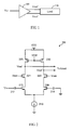
- FIG 1 illustrates a single-ended-to-differential converter 100 according to the present disclosure.
- Vout is provided to a load 110.
- the load 110 may present a low input impedance to the output of the converter 100, in which case the converter 100 may be designed to provide sufficient current drive to support the differential output voltage Vout.
- FIG 2 illustrates a baseline implementation 200 of a single-ended-to-differential converter 100.
- transistors 215 and 220 form an input differential pair, with the gate of transistor 215 AC-coupled to the input voltage Vin via capacitor 217, and the gate of transistor 220 AC-coupled to ground via capacitor 219. Note for simplicity, the DC biasing details of transistors 215 and 220 have been omitted in FIG 2 .
- the sources of transistors 215 and 220 are coupled to each other, and further to a current source 210.
- the drains of transistors 215 and 220 are coupled to the output voltages Vout - and Vout + via cascode transistors 221 and 222, respectively.
- cascode transistors 221 and 222 advantageously improve the isolation of the differential output Vout from the input Vin, thus, e.g., extending the bandwidth over which the converter 200 may operate.
- Cascode transistors 221 and 222 are DC biased by a voltage Vcas.
- the converter 200 further includes transistors 225 and 230 coupled to the output voltages Vout - and Vout + , respectively.
- a bias voltage VCM may be provided to bias the transistors 225 and 230 so that the common-mode level of the voltages Vout - and Vout + are well-defined.
- IIP3 third-order intercept point
- the IIP3 may be limited by, e.g., third-order inter-modulation (IM3) products generated in the differential output voltage Vout at the drains of transistors 221 and 222. It would be desirable to provide techniques for improving the linearity of a single-ended-to-differential converter, thereby reducing IM3 products and increasing the IIP3.
- IM3 third-order inter-modulation
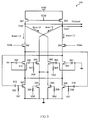
- FIG 3 illustrates an exemplary embodiment 300 of a single-ended-to-differential converter 100 according to the present disclosure.
- input transistors 315 and 320 form a differential input stage, with the gate of transistor 315 AC-coupled to the input voltage Vin via capacitor 352, and the gate of transistor 320 AC-coupled to ground via capacitor 351.
- the DC biasing details of transistors 315 and 320 have been omitted in FIG 3 .
- the drains of transistors 315 and 320 are coupled to the output voltages Vout - and Vout + via cascode transistors 330 and 335, respectively, which are further coupled to load transistors 367 and 360.
- transistors 367 and 360 may be replaced by resistors or other load elements (not shown).
- the sources of transistors 315 and 320 are coupled to each other, and further to main current source transistors 322 and 328.
- the total quiescent bias current generated by transistors 322 and 328 is also denoted herein as the main current, or Imain. It will be appreciated that in the quiescent bias condition, Imain flows through a "main path" formed by transistors 315 and 330 supporting Imain / 2, and transistors 320 and 335 also supporting Imain / 2.
- the main current source transistors 322 and 328 may be adaptively biased to improve the linearity of the input transistors 315 and 320.
- the gates of transistors 322 and 328 are each DC biased by a voltage Vb1, and further cross-coupled to the drains of transistors 320 and 315, respectively, using AC coupling capacitors 312 and 314. It will be appreciated that the AC cross-coupling of signals to the gates of transistors 322 and 328 may advantageously adjust the bias current supplied to the input transistors 315 and 320 depending on the amplitude of Vin, thus helping to maintain the linearity of the converter 300.
- the gates of transistors 345 and 350 are further AC-coupled to Vin and to AC ground, respectively, via capacitors 348 and 353.
- the drains of transistors 345 and 350 are coupled to the drains of transistors 335 and 330, respectively.
- the sources of transistors 345 and 350 are coupled to each other, and further to auxiliary current source transistors 324 and 326.
- the total current generated by transistors 324 and 326 is denoted herein as the auxiliary current, or Iaux. Iaux flows through an "auxiliary path" formed by transistors 345 and 350, wherein Iaux / 2 flows through transistor 345 and Iaux / 2 flows through transistor 350 under the quiescent bias condition.
- transistors 324 and 326 may be alternatively implemented as a single transistor current source.
- capacitors 348 and 353 are shown as coupling the gates of transistors 345 and 350 to Vin and AC ground, respectively, it will be appreciated that the capacitors 348 and 353 may be alternatively coupled.
- capacitors 348 and 353 may alternatively couple the gates of transistors 345 and 350 directly to the gates of transistors 315 and 320, respectively.
- Such alternative exemplary embodiments are contemplated to be within the scope of the present disclosure.
- transistors 345 and 350 are biased in weak inversion, with gate-to-source voltages (VGS) on the order of, e.g., 0.4 V, and threshold voltages VT on the order of, e.g., 0.55V.
- VGS gate-to-source voltages
- transistors 315 and 320 are biased in moderate inversion, with VGS on the order of, e.g., 0.6 V, and VT on the order of 0.55V.
- the supply voltage VDD may be 1.3V.
- the input signal to transistor 315 is provided with the same phase as the input signal to transistor 345, while the input signal to transistor 320 is provided with the same phase as the input signal to transistor 350. It will be appreciated that due to this configuration, the IM3 product generated by the main and auxiliary paths may be advantageously cancelled at the differential output.
- the bias voltages may be chosen such that Imain >> Iaux. In an exemplary embodiment, Imain may be on the order of 10 * Iaux.
- the current Iaux provided by transistors 324 and 326 may be further adjusted to achieve the desired level of cancellation of the third order non-linearity components.
- the bias voltage Vb2 of transistors 324 and 326 may be adjusted to achieve the desired level of cancellation.
- a single-ended-to-differential converter need not employ adaptive biasing of cross-coupling capacitors 312 and 314 in conjunction with the cascomp transistors 345 and 350 shown. Either of these features may be implemented separately from the other to perform single-ended to differential conversion. Such alternative exemplary embodiments are contemplated to be within the scope of the present disclosure.
- FIG 4 illustrates an exemplary embodiment of a receiver 400 in which the techniques of the present disclosure may be implemented. Note FIG 4 is shown for illustrative purposes only, and is not meant to limit the application of the present disclosure to receivers.
- a low-noise amplifier (LNA) 410 receives a radio-frequency (RF) signal from an antenna (not shown).
- the LNA 410 outputs an amplified version of the RF signal to a band-pass filter 420.
- the output of the band-pass filter 420 is coupled to a single-ended-to-differential converter (S2D) 430.
- S2D single-ended-to-differential converter
- the single-ended-to-differential converter 430 may be designed using the techniques previously disclosed herein.
- the differential output of the single-ended-to-differential converter 430 is provided to a mixer 440, which mixes the differential signal with a differential local oscillator signal having a frequency f LO .
- the input of the mixer 440 may present a low impedance to the output of the single-ended-to-differential converter 430.
- the output of the mixer 440 is coupled to a baseband filter 450 to generate a baseband output signal for further processing. Note the output of the mixer 440 and the baseband filter 450 may be single-ended or differential, depending on the specific architectures employed.
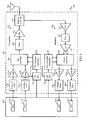
- FIG 5 illustrates a block diagram of a design of a wireless communication device 500 in which the techniques of the present disclosure may be implemented.
- FIG 5 shows an example transceiver design.
- the conditioning of the signals in a transmitter and a receiver may be performed by one or more stages of amplifier, filter, upconverter, downconverter, etc.
- These circuit blocks may be arranged differently from the configuration shown in FIG 5 .
- other circuit blocks not shown in FIG 5 may also be used to condition the signals in the transmitter and receiver. Some circuit blocks in FIG 5 may also be omitted.
- wireless device 500 includes a transceiver 520 and a data processor 510.
- the data processor 510 may include a memory (not shown) to store data and program codes.
- Transceiver 520 includes a transmitter 530 and a receiver 550 that support bi-directional communication.
- wireless device 500 may include any number of transmitters and any number of receivers for any number of communication systems and frequency bands. All or a portion of transceiver 520 may be implemented on one or more analog integrated circuits (ICs), RF ICs (RFICs), mixed-signal ICs, etc.
- ICs analog integrated circuits
- RFICs RF ICs
- mixed-signal ICs etc.
- a transmitter or a receiver may be implemented with a super-heterodyne architecture or a direct-conversion architecture.
- a signal is frequency converted between radio frequency (RF) and baseband in multiple stages, e.g., from RF to an intermediate frequency (IF) in one stage, and then from IF to baseband in another stage for a receiver.
- IF intermediate frequency
- the direct-conversion architecture a signal is frequency converted between RF and baseband in one stage.
- the super-heterodyne and direct-conversion architectures may use different circuit blocks and/or have different requirements.
- transmitter 530 and receiver 550 are implemented with the direct-conversion architecture.
- data processor 510 processes data to be transmitted and provides I and Q analog output signals to transmitter 530.
- the data processor 510 includes digital-to-analog-converters (DAC's) 514a and 514b for converting digital signals generated by the data processor 510 into the I and Q analog output signals.
- DAC's digital-to-analog-converters
- lowpass filters 532a and 532b filter the I and Q analog output signals, respectively, to remove undesired images caused by the prior digital-to-analog conversion.
- Amplifiers (Amp) 534a and 534b amplify the signals from lowpass filters 532a and 532b, respectively, and provide I and Q baseband signals.
- An upconverter 540 upconverts the I and Q baseband signals with I and Q transmit (TX) local oscillating (LO) signals from a TX LO signal generator 570 and provides an upconverted signal.
- a filter 542 filters the upconverted signal to remove undesired images caused by the frequency upconversion as well as noise in a receive frequency band.
- a power amplifier (PA) 544 amplifies the signal from filter 542 to obtain the desired output power level and provides a transmit RF signal.
- the transmit RF signal is routed through a duplexer or switch 546 and transmitted via an antenna 548.
- antenna 548 receives signals transmitted by base stations and provides a received RF signal, which is routed through duplexer or switch 546 and provided to a low noise amplifier (LNA) 552.
- LNA low noise amplifier
- the received RF signal is amplified by LNA 552 and filtered by a filter 554 to obtain a desirable RF input signal.
- the desirable RF input signal is provided to a single-ended-to-differential converter 555 (S2D), which converts the signal into a differential voltage to input to a downconverter 560.
- the S2D 555 may be designed according to the techniques of the present disclosure.
- the downconverter 560 downconverts the RF input signal with I and Q receive (RX) LO signals from an RX LO signal generator 580 and provides I and Q baseband signals.
- the I and Q baseband signals are amplified by amplifiers 562a and 562b and further filtered by lowpass filters 564a and 564b to obtain I and Q analog input signals, which are provided to data processor 510.
- the data processor 510 includes analog-to-digital-converters (ADC's) 516a and 516b for converting the analog input signals into digital signals to be further processed by the data processor 510.
- ADC's analog-to-digital-converters
- TX LO signal generator 590 generates the I and Q TX LO signals used for frequency upconversion.
- RX LO signal generator 580 generates the I and Q RX LO signals used for frequency downconversion.
- Each LO signal is a periodic signal with a particular fundamental frequency.
- a PLL 592 receives timing information from data processor 510 and generates a control signal used to adjust the frequency and/or phase of the TX LO signals from LO signal generator 590.
- a PLL 582 receives timing information from data processor 510 and generates a control signal used to adjust the frequency and/or phase of the RX LO signals from LO signal generator 580.
- FIG 6 illustrates an exemplary embodiment of a method 600 according to the present disclosure. Note the method is shown for illustrative purposes only, and is not meant to limit the scope of the present disclosure.
- a single-ended voltage is coupled to a main single-ended-to-differential converter comprising first and second input transistors and first and second cascode transistors.
- the gate of the first input transistor is coupled to a single-ended voltage
- the gate of the second input transistor is coupled to an AC ground voltage
- the sources of the first and second input transistors are biased by a main current
- the main single-ended-to-differential converter further comprises loading elements coupled to the drains of the first and second cascode transistors
- the drains of the cascode transistors are coupled to a differential output voltage.
- the drain voltages of the second and first cascode transistors are coupled to the drains of first and second cascomp transistors, respectively.
- the gate of the first cascomp transistor is coupled to the single-ended voltage
- the gate of the second cascomp transistor is coupled to an AC ground voltage
- the sources of the cascomp transistors are biased by an auxiliary current.
- a current generated by a first main current source transistor is coupled to the sources of the first and second input transistors.
- the first main current source transistor is biased by a DC voltage.
- a current generated by a second main current source transistor is coupled to the sources of the first and second input transistors.
- the second main current source transistor is biased by a DC voltage.
- the gate voltage of the first main current source transistor is coupled to the drain of the second input transistor using a first coupling capacitor.
- the gate voltage of the second main current source transistor is coupled to the drain of the first input transistor using a second coupling capacitor.
- NMOS transistors are employed for, e.g., the input transistors, cascode transistors, and cascomp transistors
- PMOS transistors may also be readily employed in alternative exemplary embodiments, with corresponding modifications made to the circuitry shown.
- MOS transistors MOSFET's
- the techniques of the present disclosure need not be limited to MOSFET-based designs, and may be readily applied to alternative exemplary embodiments (not shown) employing bipolar junction transistors (or BJT's) and/or other three-terminal transconductance devices.
- any of the comparators shown may utilize BJT's rather than MOSFET's, with the collectors, bases, and emitters of the BJT's coupled as shown for the drains, gates, and sources, respectively, of the MOSFET's.
- BJT's rather than MOSFET's
- the collectors, bases, and emitters of the BJT's coupled as shown for the drains, gates, and sources, respectively, of the MOSFET's.
- BiCMOS processes a combination of both CMOS and bipolar structures / devices may be employed to maximize the circuit performance.
- drain may encompass both the conventional meanings of those terms associated with MOSFET's, as well as the corresponding nodes of other three-terminal transconductance devices, such as BJT's, which correspondence will be evident to one of ordinary skill in the art of circuit design.
- DSP Digital Signal Processor
- ASIC Application Specific Integrated Circuit
- FPGA Field Programmable Gate Array
- a general purpose processor may be a microprocessor, but in the alternative, the processor may be any conventional processor, controller, microcontroller, or state machine.
- a processor may also be implemented as a combination of computing devices, e.g., a combination of a DSP and a microprocessor, a plurality of microprocessors, one or more microprocessors in conjunction with a DSP core, or any other such configuration.
- a software module may reside in Random Access Memory (RAM), flash memory, Read Only Memory (ROM), Electrically Programmable ROM (EPROM), Electrically Erasable Programmable ROM (EEPROM), registers, hard disk, a removable disk, a CD-ROM, or any other form of storage medium known in the art.
- An exemplary storage medium is coupled to the processor such that the processor can read information from, and write information to, the storage medium.
- the storage medium may be integral to the processor.
- the processor and the storage medium may reside in an ASIC.
- the ASIC may reside in a user terminal.
- the processor and the storage medium may reside as discrete components in a user terminal.
- the functions described may be implemented in hardware, software, firmware, or any combination thereof. If implemented in software, the functions may be stored on or transmitted over as one or more instructions or code on a computer-readable medium.
- Computer-readable media includes both computer storage media and communication media including any medium that facilitates transfer of a computer program from one place to another.
- a storage media may be any available media that can be accessed by a computer.
- such computer-readable media can comprise RAM, ROM, EEPROM, CD-ROM or other optical disk storage, magnetic disk storage or other magnetic storage devices, or any other medium that can be used to carry or store desired program code in the form of instructions or data structures and that can be accessed by a computer.
- any connection is properly termed a computer-readable medium.
- the software is transmitted from a website, server, or other remote source using a coaxial cable, fiber optic cable, twisted pair, digital subscriber line (DSL), or wireless technologies such as infrared, radio, and microwave
- the coaxial cable, fiber optic cable, twisted pair, DSL, or wireless technologies such as infrared, radio, and microwave are included in the definition of medium.
- Disk and disc includes compact disc (CD), laser disc, optical disc, digital versatile disc (DVD), floppy disk and Blu-ray disc where disks usually reproduce data magnetically, while discs reproduce data optically with lasers. Combinations of the above should also be included within the scope of computer-readable media.
Landscapes
- Engineering & Computer Science (AREA)
- Power Engineering (AREA)
- Physics & Mathematics (AREA)
- Nonlinear Science (AREA)
- Amplifiers (AREA)
Claims (13)
- Eine Vorrichtung (300) mit einem Eintakt-zu-Differential-Wandler, aufweisend:erste und zweite Eingangstransistoren (315, 320), wobei das Gate des ersten Eingangstransistors (315) mit einer Eintaktspannung gekoppelt ist und das Gate des zweiten Eingangstransistors (320) mit einer Wechselstrom (AC)-Erdspannung gekoppelt ist und wobei die ersten und zweiten Eingangstransistoren (315, 320) durch einen Hauptstrom vorgespannt sind,erste und zweite Kaskodentransistoren (330, 335), die jeweils mit den Drains der ersten und zweiten Eingangstransistoren (315, 320) gekoppelt sind,Ladeelemente, die mit den Drains der ersten und zweiten Kaskodentransistoren (330, 335) gekoppelt sind, wobei die Drains der Kaskodentransistoren (330, 335) mit einer Differentialausgangsspannung gekoppelt sind,erste und zweite Kaskomptransistoren (345, 350), wobei die Drains der ersten und zweiten Kaskomptransistoren (345, 350) jeweils mit den Drains der zweiten und ersten Kaskodentransistoren (330, 335) gekoppelt sind, wobei das Gate des ersten Kaskomptransistors (345) mit der Eintaktspannung gekoppelt ist und das Gate des zweiten Kaskomptransistors (350) mit der AC-Erdspannung gekoppelt ist,einen ersten Stromquellentransistor (322), wobei das Drain des ersten Stromquellentransistors (322) mit den Sources der ersten und zweiten Eingangstransistoren (315, 320) gekoppelt ist, wobei der erste Stromquellentransistor (322) durch eine Gleichstrom (DC)-Spannung vorgespannt ist,einen zweiten Stromquellentransistor (328), wobei das Drain des zweiten Stromquellentransistors (328) mit den Sources der ersten und zweiten Eingangstransistoren (315, 320) gekoppelt ist, wobei der zweite Stromquellentransistor (328) durch die Gleichspannung vorgespannt ist,einen ersten Kopplungskondensator (312), der das Gate des ersten Stromquellentransistors (322) mit dem Drain des zweiten Eingangstransistors (320) koppelt, undeinen zweiten Kopplungskondensator (314), der das Gate des zweiten Stromquellentransistors (328) mit dem Drain des ersten Eingangstransistors (315) koppelt,wobei die Kaskomptransistoren (345, 350) durch einen Nebenstrom vorgespannt sind, wobei der Hauptstrom größer als der Nebenstrom ist.
- Vorrichtung (300) nach Anspruch 1, wobei die ersten und zweiten Kaskomptransistoren (345, 350) in einer schwachen Inversion vorgespannt sind und die ersten und zweiten Eingangstransistoren in einer gemäßigten Inversion vorgespannt sind.
- Vorrichtung (300) nach Anspruch 2, wobei die ersten und zweiten Kaskomptransistoren (345, 350) mit Gate-zu-Source-Spannungen von 0,4 V vorgespannt sind und Schwellspannungen von 0,55 V aufweisen, wobei die ersten und zweiten Eingangstransistoren (315, 320) mit Gate-zu-Source-Spannungen von 0,6 V vorgespannt sind und Schwellwertspannungen von 0,55 V aufweisen.
- Vorrichtung (300) nach Anspruch 1, wobei die ersten und zweiten Kaskomptransistoren (345, 350) mit der Eintaktspannung und der AC-Erde unter Verwendung von Kopplungskondensatoren (352, 351) gekoppelt sind.
- Vorrichtung (300) nach Anspruch 1, wobei der Nebenstrom durch wenigstens einen Nebenstromquellentransistor (324, 326) erzeugt wird.
- Vorrichtung (300) nach Anspruch 1, wobei die Vorrichtung ein drahtloses Kommunikationsgerät ist.
- Ein Verfahren, das folgende Schritte aufweist:Koppeln (610) einer Eintaktspannung mit einem hauptsächlichen Eintakt-zu-Differential-Wandler, der erste und zweite Eingangstransistoren und erste und zweite Kaskodentransistoren aufweist, wobei das Gate des ersten Eingangstransistors mit einer Eintaktspannung gekoppelt ist, wobei das Gate des zweiten Eingangstransistors mit einer Wechselstrom (AC)-Erdspannung gekoppelt ist, wobei die Sources der ersten und zweiten Eingangstransistoren durch einen Hauptstrom vorgespannt werden, wobei der hauptsächliche Eintakt-zu-Differential-Wandler weiterhin Ladeelemente aufweist, die mit den Drains der ersten und zweiten Kaskodentransistoren gekoppelt sind, wobei die Drains der Kaskodentransistoren mit einer Differentialausgangsspannung gekoppelt sind,Koppeln (620) der Drainspannungen der zweiten und ersten Kaskodentransistoren jeweils mit Drains der ersten und zweiten Kaskomptransistoren, wobei das Gate des ersten Kaskomptransistors mit der Eintaktspannung gekoppelt ist und wobei das Gate des zweiten Kaskomptransistors mit der AC-Erdspannung gekoppelt ist,Koppeln (630) eines durch einen ersten Stromquellentransistor erzeugten Stroms mit den Sources der ersten und zweiten Eingangstransistoren, wobei der erste Stromquellentransistor durch eine Gleichstrom (DC)-Spannung vorgespannt ist,Koppeln (640) eines durch einen zweiten Stromquellentransistor erzeugten Stroms mit den Sources der ersten und zweiten Eingangstransistoren, wobei der zweite Stromquellentransistor durch die DC-Spannung vorgespannt ist,Koppeln (650) der Gate-Spannug des ersten Stromquellentransistors mit dem Drain des zweiten Eingangstransistors unter Verwendung eines ersten Kopplungskondensators, undKoppeln (660) der Gate-Spannung des zweiten Stromquellentransistors mit dem Drain des ersten Eingangstransistors unter Verwendung eines zweiten Kopplungskondensators,wobei die Sources der Kaskomptransistoren durch einen Nebenstrom vorgespannt sind, wobei der Hauptstrom größer als der Nebenstrom ist.
- Verfahren nach Anspruch 7, das weiterhin Schritte aufweist zum Vorspannen der ersten und zweiten Kaskomptransistoren in einer schwachen Inversion und zum Vorspannen der ersten und zweiten Eingangstransistoren in einer gemäßigten Inversion.
- Verfahren nach Anspruch 8, das weiterhin Schritte aufweist zum Vorspannen der ersten und zweiten Kaskomptransistoren mit Gate-zu-Source-Spannungen von 0,4 V, wobei die ersten und zweiten Kaskomptransistoren Schwellspannungen von 0,55 V aufweisen, und zum Vorspannen der ersten und zweiten Eingangstransistoren mit Gate-zu-Source-Spannungen von 0,6 V, wobei die ersten und zweiten Eingangstransistoren Schwellspannungen von 0,55 V aufweisen.
- Verfahren nach Anspruch 7, das weiterhin einen Schritt aufweist zum Koppeln der ersten und zweiten Kaskomptransistoren mit der Eintaktspannung und der AC-Erde unter Verwendung von Kopplungskondensatoren.
- Verfahren nach Anspruch 7, das weiterhin einen Schritt aufweist zum Erzeugen des Nebenstroms unter Verwendung wenigstens eines Nebenstromquellentransistors.
- Verfahren nach Anspruch 7 oder Vorrichtung nach Anspruch 1, wobei die Ladelemente Transistoren aufweisen, die unter Verwendung einer Spannung vorgespannt sind, um eine Gemeinsamer-Modus-Ausgangsspannung an den Drains der Kaskodentransistoren zu erzeugen.
- Verfahren nach Anspruch 7 oder Vorrichtung nach Anspruch 1, wobei die Ladelemente Widerstände aufweisen.
Applications Claiming Priority (3)
| Application Number | Priority Date | Filing Date | Title |
|---|---|---|---|
| US22104809P | 2009-06-27 | 2009-06-27 | |
| US12/606,003 US8421541B2 (en) | 2009-06-27 | 2009-10-26 | RF single-ended to differential converter |
| PCT/US2010/040246 WO2010151889A2 (en) | 2009-06-27 | 2010-06-28 | Rf single-ended to differential converter |
Publications (2)
| Publication Number | Publication Date |
|---|---|
| EP2446531A2 EP2446531A2 (de) | 2012-05-02 |
| EP2446531B1 true EP2446531B1 (de) | 2014-07-16 |
Family
ID=43380625
Family Applications (1)
| Application Number | Title | Priority Date | Filing Date |
|---|---|---|---|
| EP10740461.8A Active EP2446531B1 (de) | 2009-06-27 | 2010-06-28 | Eintakt-zu-differenzial-hochfrequenzwandler |
Country Status (6)
| Country | Link |
|---|---|
| US (1) | US8421541B2 (de) |
| EP (1) | EP2446531B1 (de) |
| JP (1) | JP5485386B2 (de) |
| CN (1) | CN102460959B (de) |
| TW (1) | TW201126899A (de) |
| WO (1) | WO2010151889A2 (de) |
Families Citing this family (23)
| Publication number | Priority date | Publication date | Assignee | Title |
|---|---|---|---|---|
| TWI441461B (zh) * | 2011-05-20 | 2014-06-11 | Sunplus Technology Co Ltd | 具可適應性濾波器的通用接收裝置 |
| CN102811067A (zh) * | 2011-06-02 | 2012-12-05 | 凌阳科技股份有限公司 | 具可适应性滤波器的通用接收装置 |
| KR101821820B1 (ko) * | 2011-11-09 | 2018-03-08 | 삼성전자주식회사 | 다채널 접촉 센싱 장치 |
| KR101873754B1 (ko) * | 2011-11-25 | 2018-07-04 | 한국전자통신연구원 | 고주파 수신기 |
| US9030262B2 (en) | 2012-04-03 | 2015-05-12 | Samsung Electronics Co., Ltd. | Input receiver circuit having single-to-differential amplifier, and semiconductor device including the same |
| US9588533B2 (en) | 2012-07-31 | 2017-03-07 | Entropic Communications, Llc | High unity gain bandwidth voltage regulation for integrated circuits |
| US9130517B2 (en) | 2012-10-05 | 2015-09-08 | Qualcomm Incorporated | Systems and methods of harmonic extraction and rejection |
| US9124246B2 (en) | 2013-09-25 | 2015-09-01 | Qualcomm Incorporated | Baseband processing circuitry |
| US10128879B2 (en) * | 2014-03-31 | 2018-11-13 | Intel IP Corporation | Enhanced receive sensitivity for concurrent communications |
| KR101609692B1 (ko) | 2014-07-23 | 2016-04-08 | 한국항공대학교산학협력단 | 저잡음 증폭기 |
| US9384371B2 (en) | 2014-10-28 | 2016-07-05 | King Fahd University Of Petroleum And Minerals | Compact CMOS current-mode analog multifunction circuit |
| US9503053B1 (en) | 2015-05-13 | 2016-11-22 | Qualcomm Incorporated | Active balun for wideband applications |
| CN106374924B (zh) | 2015-07-22 | 2021-05-25 | 三星电子株式会社 | 使用模数转换器执行共模电压补偿的半导体器件 |
| US9584073B1 (en) * | 2015-10-07 | 2017-02-28 | GM Global Technology Operations LLC | Internally matched active single-to-differential RF converter |
| EP3258597B1 (de) * | 2016-06-13 | 2020-07-29 | Intel IP Corporation | Verstärkerschaltung, vorrichtung zur verstärkung, rauscharmer verstärker, funkempfänger, mobiles endgerät, basisstation und verfahren zur verstärkung |
| US10110223B2 (en) * | 2016-07-06 | 2018-10-23 | Via Alliance Semiconductor Co., Ltd. | Single ended-to-differential converter |
| JP2019122001A (ja) * | 2018-01-11 | 2019-07-22 | 株式会社東芝 | 回路、受信回路、光受信器、光伝送システム、およびアクティブ光ケーブル |
| TWI690131B (zh) * | 2018-04-26 | 2020-04-01 | 國立暨南國際大學 | 射頻/直流轉換器 |
| US10530618B1 (en) | 2018-09-26 | 2020-01-07 | Qualcomm Incorporated | Single-ended to differential signal conversion of analog signals |
| US11646700B2 (en) * | 2021-06-21 | 2023-05-09 | Texas Instruments Incorporated | Amplifiers with feedforward cancellation |
| WO2021232030A1 (en) * | 2021-07-14 | 2021-11-18 | Futurewei Technologies, Inc. | Active balun amplifier |
| US11863205B2 (en) | 2021-11-30 | 2024-01-02 | Analog Devices International Unlimited Company | Adaptive bias techniques for amplifiers in sigma delta modulators |
| CN115225077B (zh) * | 2022-07-29 | 2025-07-08 | 西安理工大学 | 一种用于抵抗电源和阈值扰动的电平转换电路 |
Family Cites Families (25)
| Publication number | Priority date | Publication date | Assignee | Title |
|---|---|---|---|---|
| US4146844A (en) * | 1977-10-31 | 1979-03-27 | Tektronix, Inc. | Feed-forward amplifier |
| US4528517A (en) * | 1983-02-07 | 1985-07-09 | Tektronix, Inc. | Overdrive thermal distortion compensation for a Quinn cascomp amplifier |
| US5250911A (en) * | 1992-04-20 | 1993-10-05 | Hughes Aircraft Company | Single-ended and differential transistor amplifier circuits with full signal modulation compensation techniques which are technology independent |
| US6525609B1 (en) | 1998-11-12 | 2003-02-25 | Broadcom Corporation | Large gain range, high linearity, low noise MOS VGA |
| US7696823B2 (en) | 1999-05-26 | 2010-04-13 | Broadcom Corporation | System and method for linearizing a CMOS differential pair |
| US6566961B2 (en) | 2001-03-30 | 2003-05-20 | Institute Of Microelectronics | Wide-band single-ended to differential converter in CMOS technology |
| US6853838B2 (en) | 2001-05-14 | 2005-02-08 | National Semiconductor Corporation | Biasing circuit for degenerated differential pair |
| WO2002103898A1 (en) | 2001-06-14 | 2002-12-27 | Nurlogic Design, Inc. | Method and apparatus for voltage clamping in feedback amplifiers using resistors |
| US6794938B2 (en) * | 2002-03-19 | 2004-09-21 | The University Of North Carolina At Charlotte | Method and apparatus for cancellation of third order intermodulation distortion and other nonlinearities |
| EP1611677A1 (de) | 2003-03-28 | 2006-01-04 | Koninklijke Philips Electronics N.V. | Neutralisierung der rückkopplungskapazität in verstärkern |
| US6992519B2 (en) | 2004-02-11 | 2006-01-31 | Nokia Corporation | Method and apparatus providing cancellation of second order intermodulation distortion and enhancement of second order intercept point (IIP2) in common source and common emitter transconductance circuits |
| US7071779B2 (en) * | 2004-06-17 | 2006-07-04 | Winbond Electronics, Corp. | Monolithic CMOS differential LNA with enhanced linearity |
| JP2006129416A (ja) * | 2004-09-28 | 2006-05-18 | Sharp Corp | 電圧−電流変換回路、それを用いた増幅器、ミキサ回路および携帯機器 |
| JP4141433B2 (ja) * | 2004-11-29 | 2008-08-27 | 株式会社シンセシス | 差動増幅回路 |
| US7459974B2 (en) | 2004-12-16 | 2008-12-02 | Anadigics, Inc. | System and method for distortion cancellation in amplifiers |
| KR100729342B1 (ko) | 2005-02-17 | 2007-06-15 | 삼성전자주식회사 | dB 선형 이득의 제어가 가능한 CMOS 가변 이득 증폭기 |
| JP4935003B2 (ja) * | 2005-06-30 | 2012-05-23 | アイコム株式会社 | 可変利得増幅器及び差動増幅器 |
| DE102005062767A1 (de) | 2005-12-28 | 2007-07-12 | Atmel Germany Gmbh | Kaskoden-Differenzverstärker und Differenzverstärker |
| TWI335128B (en) | 2006-03-01 | 2010-12-21 | Princeton Technology Corp | Single-end input to differential-ends output low noise amplifier |
| JP2008061126A (ja) * | 2006-09-01 | 2008-03-13 | Sharp Corp | 増幅回路 |
| US7538618B2 (en) | 2006-12-05 | 2009-05-26 | Electronics And Telecommunications Research Institute | Wideband active balun circuit based on differential amplifier |
| US8086207B2 (en) | 2007-03-19 | 2011-12-27 | Qualcomm Incorporated | Linear transconductor for RF communications |
| US7671686B2 (en) * | 2007-10-24 | 2010-03-02 | Industrial Technology Research Institute | Low noise amplifier |
| US7944298B2 (en) * | 2007-12-18 | 2011-05-17 | Qualcomm, Incorporated | Low noise and low input capacitance differential MDS LNA |
| KR100956000B1 (ko) | 2008-02-29 | 2010-05-04 | 성균관대학교산학협력단 | 선형성을 개선하기 위한 차동증폭회로 및 주파수 혼합기 |
-
2009
- 2009-10-26 US US12/606,003 patent/US8421541B2/en active Active
-
2010
- 2010-06-25 TW TW099120952A patent/TW201126899A/zh unknown
- 2010-06-28 WO PCT/US2010/040246 patent/WO2010151889A2/en not_active Ceased
- 2010-06-28 CN CN201080028858.9A patent/CN102460959B/zh active Active
- 2010-06-28 JP JP2012517832A patent/JP5485386B2/ja not_active Expired - Fee Related
- 2010-06-28 EP EP10740461.8A patent/EP2446531B1/de active Active
Also Published As
| Publication number | Publication date |
|---|---|
| US20100329158A1 (en) | 2010-12-30 |
| CN102460959B (zh) | 2014-08-27 |
| JP5485386B2 (ja) | 2014-05-07 |
| EP2446531A2 (de) | 2012-05-02 |
| US8421541B2 (en) | 2013-04-16 |
| CN102460959A (zh) | 2012-05-16 |
| WO2010151889A3 (en) | 2011-06-16 |
| JP2012531836A (ja) | 2012-12-10 |
| WO2010151889A2 (en) | 2010-12-29 |
| TW201126899A (en) | 2011-08-01 |
Similar Documents
| Publication | Publication Date | Title |
|---|---|---|
| US8421541B2 (en) | RF single-ended to differential converter | |
| US8031005B2 (en) | Amplifier supporting multiple gain modes | |
| US7902923B2 (en) | Common-gate common-source amplifier | |
| US8102213B2 (en) | Multi-mode low noise amplifier with transformer source degeneration | |
| US7834698B2 (en) | Amplifier with improved linearization | |
| US20120064852A1 (en) | Low noise amplifier having both ultra-high linearity and low noise characteristic and radio receiver including the same | |
| US20110037518A1 (en) | Amplifiers with improved linearity and noise performance | |
| US20100156532A1 (en) | Class ab amplifier with resistive level-shifting circuitry | |
| US20070096830A1 (en) | Wideband circuits and methods | |
| WO2010068811A1 (en) | Amplifier with programmable off voltage | |
| CN111987998A (zh) | 一种噪声抵消低噪声放大器 | |
| Bai et al. | A 35-dBm OIP3 CMOS constant bandwidth PGA with extended input range and improved common-mode rejection | |
| Bai et al. | A review of CMOS variable gain amplifiers and programmable gain amplifiers | |
| Lei et al. | A Power-Efficient Active-RC Filter Using Passive Integrator and OTA With Push-Pull Output | |
| CN212695961U (zh) | 一种噪声抵消低噪声放大器 | |
| US11303250B2 (en) | High linearity low noise amplifier | |
| CN118157597B (zh) | 全差分两级驱动放大电路、物联网芯片及电子设备 | |
| KR101609692B1 (ko) | 저잡음 증폭기 |
Legal Events
| Date | Code | Title | Description |
|---|---|---|---|
| PUAI | Public reference made under article 153(3) epc to a published international application that has entered the european phase |
Free format text: ORIGINAL CODE: 0009012 |
|
| 17P | Request for examination filed |
Effective date: 20120127 |
|
| AK | Designated contracting states |
Kind code of ref document: A2 Designated state(s): AL AT BE BG CH CY CZ DE DK EE ES FI FR GB GR HR HU IE IS IT LI LT LU LV MC MK MT NL NO PL PT RO SE SI SK SM TR |
|
| DAX | Request for extension of the european patent (deleted) | ||
| 17Q | First examination report despatched |
Effective date: 20121106 |
|
| GRAP | Despatch of communication of intention to grant a patent |
Free format text: ORIGINAL CODE: EPIDOSNIGR1 |
|
| INTG | Intention to grant announced |
Effective date: 20140129 |
|
| GRAS | Grant fee paid |
Free format text: ORIGINAL CODE: EPIDOSNIGR3 |
|
| GRAA | (expected) grant |
Free format text: ORIGINAL CODE: 0009210 |
|
| AK | Designated contracting states |
Kind code of ref document: B1 Designated state(s): AL AT BE BG CH CY CZ DE DK EE ES FI FR GB GR HR HU IE IS IT LI LT LU LV MC MK MT NL NO PL PT RO SE SI SK SM TR |
|
| REG | Reference to a national code |
Ref country code: GB Ref legal event code: FG4D |
|
| REG | Reference to a national code |
Ref country code: CH Ref legal event code: EP |
|
| REG | Reference to a national code |
Ref country code: IE Ref legal event code: FG4D |
|
| REG | Reference to a national code |
Ref country code: AT Ref legal event code: REF Ref document number: 678164 Country of ref document: AT Kind code of ref document: T Effective date: 20140815 |
|
| REG | Reference to a national code |
Ref country code: DE Ref legal event code: R096 Ref document number: 602010017529 Country of ref document: DE Effective date: 20140828 |
|
| REG | Reference to a national code |
Ref country code: NL Ref legal event code: VDEP Effective date: 20141210 |
|
| REG | Reference to a national code |
Ref country code: AT Ref legal event code: MK05 Ref document number: 678164 Country of ref document: AT Kind code of ref document: T Effective date: 20140716 |
|
| REG | Reference to a national code |
Ref country code: LT Ref legal event code: MG4D |
|
| PG25 | Lapsed in a contracting state [announced via postgrant information from national office to epo] |
Ref country code: NO Free format text: LAPSE BECAUSE OF FAILURE TO SUBMIT A TRANSLATION OF THE DESCRIPTION OR TO PAY THE FEE WITHIN THE PRESCRIBED TIME-LIMIT Effective date: 20141016 Ref country code: ES Free format text: LAPSE BECAUSE OF FAILURE TO SUBMIT A TRANSLATION OF THE DESCRIPTION OR TO PAY THE FEE WITHIN THE PRESCRIBED TIME-LIMIT Effective date: 20140716 Ref country code: SE Free format text: LAPSE BECAUSE OF FAILURE TO SUBMIT A TRANSLATION OF THE DESCRIPTION OR TO PAY THE FEE WITHIN THE PRESCRIBED TIME-LIMIT Effective date: 20140716 Ref country code: BG Free format text: LAPSE BECAUSE OF FAILURE TO SUBMIT A TRANSLATION OF THE DESCRIPTION OR TO PAY THE FEE WITHIN THE PRESCRIBED TIME-LIMIT Effective date: 20141016 Ref country code: GR Free format text: LAPSE BECAUSE OF FAILURE TO SUBMIT A TRANSLATION OF THE DESCRIPTION OR TO PAY THE FEE WITHIN THE PRESCRIBED TIME-LIMIT Effective date: 20141017 Ref country code: FI Free format text: LAPSE BECAUSE OF FAILURE TO SUBMIT A TRANSLATION OF THE DESCRIPTION OR TO PAY THE FEE WITHIN THE PRESCRIBED TIME-LIMIT Effective date: 20140716 Ref country code: LT Free format text: LAPSE BECAUSE OF FAILURE TO SUBMIT A TRANSLATION OF THE DESCRIPTION OR TO PAY THE FEE WITHIN THE PRESCRIBED TIME-LIMIT Effective date: 20140716 Ref country code: PT Free format text: LAPSE BECAUSE OF FAILURE TO SUBMIT A TRANSLATION OF THE DESCRIPTION OR TO PAY THE FEE WITHIN THE PRESCRIBED TIME-LIMIT Effective date: 20141117 |
|
| PG25 | Lapsed in a contracting state [announced via postgrant information from national office to epo] |
Ref country code: PL Free format text: LAPSE BECAUSE OF FAILURE TO SUBMIT A TRANSLATION OF THE DESCRIPTION OR TO PAY THE FEE WITHIN THE PRESCRIBED TIME-LIMIT Effective date: 20140716 Ref country code: CY Free format text: LAPSE BECAUSE OF FAILURE TO SUBMIT A TRANSLATION OF THE DESCRIPTION OR TO PAY THE FEE WITHIN THE PRESCRIBED TIME-LIMIT Effective date: 20140716 Ref country code: LV Free format text: LAPSE BECAUSE OF FAILURE TO SUBMIT A TRANSLATION OF THE DESCRIPTION OR TO PAY THE FEE WITHIN THE PRESCRIBED TIME-LIMIT Effective date: 20140716 Ref country code: NL Free format text: LAPSE BECAUSE OF FAILURE TO SUBMIT A TRANSLATION OF THE DESCRIPTION OR TO PAY THE FEE WITHIN THE PRESCRIBED TIME-LIMIT Effective date: 20140716 Ref country code: IS Free format text: LAPSE BECAUSE OF FAILURE TO SUBMIT A TRANSLATION OF THE DESCRIPTION OR TO PAY THE FEE WITHIN THE PRESCRIBED TIME-LIMIT Effective date: 20141116 Ref country code: AT Free format text: LAPSE BECAUSE OF FAILURE TO SUBMIT A TRANSLATION OF THE DESCRIPTION OR TO PAY THE FEE WITHIN THE PRESCRIBED TIME-LIMIT Effective date: 20140716 |
|
| REG | Reference to a national code |
Ref country code: DE Ref legal event code: R097 Ref document number: 602010017529 Country of ref document: DE |
|
| PG25 | Lapsed in a contracting state [announced via postgrant information from national office to epo] |
Ref country code: SK Free format text: LAPSE BECAUSE OF FAILURE TO SUBMIT A TRANSLATION OF THE DESCRIPTION OR TO PAY THE FEE WITHIN THE PRESCRIBED TIME-LIMIT Effective date: 20140716 Ref country code: CZ Free format text: LAPSE BECAUSE OF FAILURE TO SUBMIT A TRANSLATION OF THE DESCRIPTION OR TO PAY THE FEE WITHIN THE PRESCRIBED TIME-LIMIT Effective date: 20140716 Ref country code: RO Free format text: LAPSE BECAUSE OF FAILURE TO SUBMIT A TRANSLATION OF THE DESCRIPTION OR TO PAY THE FEE WITHIN THE PRESCRIBED TIME-LIMIT Effective date: 20140716 Ref country code: DK Free format text: LAPSE BECAUSE OF FAILURE TO SUBMIT A TRANSLATION OF THE DESCRIPTION OR TO PAY THE FEE WITHIN THE PRESCRIBED TIME-LIMIT Effective date: 20140716 Ref country code: EE Free format text: LAPSE BECAUSE OF FAILURE TO SUBMIT A TRANSLATION OF THE DESCRIPTION OR TO PAY THE FEE WITHIN THE PRESCRIBED TIME-LIMIT Effective date: 20140716 Ref country code: IT Free format text: LAPSE BECAUSE OF FAILURE TO SUBMIT A TRANSLATION OF THE DESCRIPTION OR TO PAY THE FEE WITHIN THE PRESCRIBED TIME-LIMIT Effective date: 20140716 |
|
| PLBE | No opposition filed within time limit |
Free format text: ORIGINAL CODE: 0009261 |
|
| STAA | Information on the status of an ep patent application or granted ep patent |
Free format text: STATUS: NO OPPOSITION FILED WITHIN TIME LIMIT |
|
| 26N | No opposition filed |
Effective date: 20150417 |
|
| PG25 | Lapsed in a contracting state [announced via postgrant information from national office to epo] |
Ref country code: SI Free format text: LAPSE BECAUSE OF FAILURE TO SUBMIT A TRANSLATION OF THE DESCRIPTION OR TO PAY THE FEE WITHIN THE PRESCRIBED TIME-LIMIT Effective date: 20140716 |
|
| PG25 | Lapsed in a contracting state [announced via postgrant information from national office to epo] |
Ref country code: MC Free format text: LAPSE BECAUSE OF FAILURE TO SUBMIT A TRANSLATION OF THE DESCRIPTION OR TO PAY THE FEE WITHIN THE PRESCRIBED TIME-LIMIT Effective date: 20140716 |
|
| REG | Reference to a national code |
Ref country code: CH Ref legal event code: PL |
|
| PG25 | Lapsed in a contracting state [announced via postgrant information from national office to epo] |
Ref country code: LU Free format text: LAPSE BECAUSE OF FAILURE TO SUBMIT A TRANSLATION OF THE DESCRIPTION OR TO PAY THE FEE WITHIN THE PRESCRIBED TIME-LIMIT Effective date: 20150628 |
|
| REG | Reference to a national code |
Ref country code: IE Ref legal event code: MM4A |
|
| REG | Reference to a national code |
Ref country code: FR Ref legal event code: ST Effective date: 20160229 |
|
| PG25 | Lapsed in a contracting state [announced via postgrant information from national office to epo] |
Ref country code: LI Free format text: LAPSE BECAUSE OF NON-PAYMENT OF DUE FEES Effective date: 20150630 Ref country code: CH Free format text: LAPSE BECAUSE OF NON-PAYMENT OF DUE FEES Effective date: 20150630 Ref country code: IE Free format text: LAPSE BECAUSE OF NON-PAYMENT OF DUE FEES Effective date: 20150628 |
|
| PG25 | Lapsed in a contracting state [announced via postgrant information from national office to epo] |
Ref country code: FR Free format text: LAPSE BECAUSE OF NON-PAYMENT OF DUE FEES Effective date: 20150630 |
|
| PG25 | Lapsed in a contracting state [announced via postgrant information from national office to epo] |
Ref country code: BE Free format text: LAPSE BECAUSE OF FAILURE TO SUBMIT A TRANSLATION OF THE DESCRIPTION OR TO PAY THE FEE WITHIN THE PRESCRIBED TIME-LIMIT Effective date: 20140716 |
|
| PG25 | Lapsed in a contracting state [announced via postgrant information from national office to epo] |
Ref country code: MT Free format text: LAPSE BECAUSE OF FAILURE TO SUBMIT A TRANSLATION OF THE DESCRIPTION OR TO PAY THE FEE WITHIN THE PRESCRIBED TIME-LIMIT Effective date: 20140716 |
|
| PG25 | Lapsed in a contracting state [announced via postgrant information from national office to epo] |
Ref country code: HU Free format text: LAPSE BECAUSE OF FAILURE TO SUBMIT A TRANSLATION OF THE DESCRIPTION OR TO PAY THE FEE WITHIN THE PRESCRIBED TIME-LIMIT; INVALID AB INITIO Effective date: 20100628 Ref country code: SM Free format text: LAPSE BECAUSE OF FAILURE TO SUBMIT A TRANSLATION OF THE DESCRIPTION OR TO PAY THE FEE WITHIN THE PRESCRIBED TIME-LIMIT Effective date: 20140716 |
|
| PG25 | Lapsed in a contracting state [announced via postgrant information from national office to epo] |
Ref country code: HR Free format text: LAPSE BECAUSE OF FAILURE TO SUBMIT A TRANSLATION OF THE DESCRIPTION OR TO PAY THE FEE WITHIN THE PRESCRIBED TIME-LIMIT Effective date: 20140716 |
|
| PG25 | Lapsed in a contracting state [announced via postgrant information from national office to epo] |
Ref country code: TR Free format text: LAPSE BECAUSE OF FAILURE TO SUBMIT A TRANSLATION OF THE DESCRIPTION OR TO PAY THE FEE WITHIN THE PRESCRIBED TIME-LIMIT Effective date: 20140716 |
|
| PG25 | Lapsed in a contracting state [announced via postgrant information from national office to epo] |
Ref country code: MK Free format text: LAPSE BECAUSE OF FAILURE TO SUBMIT A TRANSLATION OF THE DESCRIPTION OR TO PAY THE FEE WITHIN THE PRESCRIBED TIME-LIMIT Effective date: 20140716 |
|
| PG25 | Lapsed in a contracting state [announced via postgrant information from national office to epo] |
Ref country code: AL Free format text: LAPSE BECAUSE OF FAILURE TO SUBMIT A TRANSLATION OF THE DESCRIPTION OR TO PAY THE FEE WITHIN THE PRESCRIBED TIME-LIMIT Effective date: 20140716 |
|
| PGFP | Annual fee paid to national office [announced via postgrant information from national office to epo] |
Ref country code: DE Payment date: 20250509 Year of fee payment: 16 |
|
| PGFP | Annual fee paid to national office [announced via postgrant information from national office to epo] |
Ref country code: GB Payment date: 20250508 Year of fee payment: 16 |