EP2437287A1 - Method for producing diode, and diode - Google Patents
Method for producing diode, and diode Download PDFInfo
- Publication number
- EP2437287A1 EP2437287A1 EP09845213A EP09845213A EP2437287A1 EP 2437287 A1 EP2437287 A1 EP 2437287A1 EP 09845213 A EP09845213 A EP 09845213A EP 09845213 A EP09845213 A EP 09845213A EP 2437287 A1 EP2437287 A1 EP 2437287A1
- Authority
- EP
- European Patent Office
- Prior art keywords
- type semiconductor
- concentration
- semiconductor layer
- layer
- medium
- Prior art date
- Legal status (The legal status is an assumption and is not a legal conclusion. Google has not performed a legal analysis and makes no representation as to the accuracy of the status listed.)
- Withdrawn
Links
Images



Classifications
-
- H—ELECTRICITY
- H10—SEMICONDUCTOR DEVICES; ELECTRIC SOLID-STATE DEVICES NOT OTHERWISE PROVIDED FOR
- H10P—GENERIC PROCESSES OR APPARATUS FOR THE MANUFACTURE OR TREATMENT OF DEVICES COVERED BY CLASS H10
- H10P10/00—Bonding of wafers, substrates or parts of devices
-
- H—ELECTRICITY
- H10—SEMICONDUCTOR DEVICES; ELECTRIC SOLID-STATE DEVICES NOT OTHERWISE PROVIDED FOR
- H10D—INORGANIC ELECTRIC SEMICONDUCTOR DEVICES
- H10D8/00—Diodes
-
- H—ELECTRICITY
- H10—SEMICONDUCTOR DEVICES; ELECTRIC SOLID-STATE DEVICES NOT OTHERWISE PROVIDED FOR
- H10D—INORGANIC ELECTRIC SEMICONDUCTOR DEVICES
- H10D8/00—Diodes
- H10D8/01—Manufacture or treatment
- H10D8/045—Manufacture or treatment of PN junction diodes
-
- H—ELECTRICITY
- H10—SEMICONDUCTOR DEVICES; ELECTRIC SOLID-STATE DEVICES NOT OTHERWISE PROVIDED FOR
- H10D—INORGANIC ELECTRIC SEMICONDUCTOR DEVICES
- H10D8/00—Diodes
- H10D8/50—PIN diodes
-
- H—ELECTRICITY
- H10—SEMICONDUCTOR DEVICES; ELECTRIC SOLID-STATE DEVICES NOT OTHERWISE PROVIDED FOR
- H10D—INORGANIC ELECTRIC SEMICONDUCTOR DEVICES
- H10D62/00—Semiconductor bodies, or regions thereof, of devices having potential barriers
- H10D62/60—Impurity distributions or concentrations
Definitions
- the present application relates to a method of manufacturing a diode, and the diode.
- Japanese Patent Application Laid-Open No. 2000-228404 discloses a diode comprising a high concentration n-type semiconductor layer, a medium concentration n-type semiconductor layer formed on the high concentration n-type semiconductor layer, a low concentration n-type semiconductor layer formed on the medium concentration n-type semiconductor layer, and a p-type semiconductor layer formed on the low concentration n-type semiconductor layer.
- this diode is switched from the state where the forward voltage is applied to the state where the reverse voltage applied, the spread of a depletion layer stops at the medium concentration n-type semiconductor layer, since a concentration of n-type impurities of the medium concentration n-type semiconductor layer is relatively high.
- the medium concentration n-type semiconductor layer is partially depleted, but is not completely depleted. Therefore, the carriers remain in the medium concentration n-type semiconductor layer which is not depleted, and the rapid exhaustion of the carriers is suppressed. As a consequence, the recovery surge voltage decreases.
- Japanese Patent Application Laid-Open No. 2000-228404 discloses two methods of manufacturing the above mentioned diode.
- the medium concentration n-type semiconductor layer and the low concentration n-type semiconductor layer are grown on a semiconductor substrate, which corresponds to the high concentration n-type semiconductor layer, by epitaxial growth.
- a very thick layer is grown by the epitaxial growth. It takes a long time to form a thick layer by the epitaxial growth.
- crystal defects, such as slippage are easily generated, and the manufacturing yield drops. Consequently, according to the first manufacturing method, diodes cannot be manufactured efficiently.
- n-type impurities are injected to the semiconductor substrate, which corresponds to the low concentration n-type semiconductor layer, to form the medium concentration n-type semiconductor layer and the high concentration n-type semiconductor layer.
- the thick medium concentration n-type semiconductor layer it is difficult to form the thick medium concentration n-type semiconductor layer by ion injection. If the thickness of the medium concentration n-type semiconductor layer is thin, the recovery surge voltage does not decrease. If the quantity of the n-type impurities to be injected is increased and the thermal diffusion time of the impurities is increased, the medium concentration n-type semiconductor region can be formed to be thick. But if the medium concentration n-type semiconductor layer is formed to be thick in this manner, it takes time to manufacture a diode.
- the present specification provides a method of efficiently manufacturing a diode of which recovery surge voltage is hardly generated.
- a diode including: a high concentration n-type semiconductor layer; a medium concentration n-type semiconductor layer formed on the high concentration n-type semiconductor layer; a low concentration n-type semiconductor layer formed on the medium concentration n-type semiconductor layer; and a p-type semiconductor layer formed on the low concentration n-type semiconductor layer, is manufactured.
- the manufacturing method includes: growing the low concentration n-type semiconductor layer on an n-type semiconductor substrate by epitaxial growth, wherein a concentration of n-type impurities in the low concentration n-type semiconductor layer is lower than that in the n-type semiconductor substrate; and forming the high concentration n-type semiconductor layer by injecting n-type impurities to a lower surface of the n-type semiconductor substrate.
- the p-type semiconductor layer may be formed by either epitaxial growth or impurity injection.
- the step of forming the p-type semiconductor layer must be executed after the step of forming the low concentration n-type semiconductor layer, but may be executed before the step of forming the high concentration n-type semiconductor layer or may be executed after this step.
- the low concentration n-type semiconductor layer is grown on the n-type semiconductor substrate by the epitaxial growth. Since the layer to be grown by the epitaxial growth is one, the epitaxial growth does not take a long time.
- the high concentration n-type semiconductor layer is formed by injecting n-type impurities to the n-type semiconductor substrate.
- the high concentration n-type semiconductor layer which need not be formed to be thick, can be formed appropriately by injecting the n-type impurities.
- a region in the n-type semiconductor substrate that is other than the high concentration n-type semiconductor layer becomes the medium concentration n-type semiconductor layer, in which the concentration of n-type impurities is higher than that of the low concentration n-type semiconductor layer, and in which the concentration of n-type impurities is lower than that of the high concentration n-type semiconductor layer.
- the thickness of the medium concentration n-type semiconductor layer is determined depending on the thickness of the n-type semiconductor substrate to be used. Therefore, it is easy to increase the thickness of the medium concentration n-type semiconductor layer.
- the medium concentration n-type semiconductor layer can be formed to be thick, and a diode in which recovery surge voltage is hardly generated can be manufactured. Further, according to the first manufacturing method, it is unnecessary to perform the epitaxial growth and the n-type impurity injection for a long time, hence diodes can be manufactured efficiently.
- the medium concentration n-type semiconductor layer is formed using the n-type semiconductor substrate.
- the manufacturing variation in the concentration of n-type impurities in the n-type semiconductor substrate is large.
- the concentration of n-type impurities changes along the pulling direction of the ingot. Therefore, the manufacturing variation in the concentration of n-type impurities is large in the n-type semiconductor substrates, which are sliced from the ingot.
- the concentration of n-type impurities differs depending on a position in the n-type semiconductor substrate. Since a variation resides in the concentration of n-type impurities in the n-type semiconductor substrate, as described above, variation in the concentration of n-type impurities in the medium concentration n-type semiconductor layer is also large. If the variation in the n-type impurity concentration of the medium concentration n-type semiconductor layer is large, a range of a depletion layer spreading in the medium concentration n-type semiconductor layer varies.
- the present specification provides a second manufacturing method for suppressing the variation in the characteristics of the recovery surge voltage.
- a diode including: a high concentration n-type semiconductor layer; a first medium concentration n-type semiconductor layer formed on the high concentration n-type semiconductor layer; a second medium concentration n-type semiconductor layer formed on the first medium concentration n-type semiconductor layer; a low concentration n-type semiconductor layer formed on the second medium concentration n-type semiconductor layer; and a p-type semiconductor layer formed on the low concentration n-type semiconductor layer, is manufactured.
- This manufacturing method includes: growing the second medium concentration n-type semiconductor layer on an n-type semiconductor substrate by epitaxial growth; growing the low concentration n-type semiconductor layer on the second medium concentration n-type semiconductor layer by epitaxial growth, wherein a concentration of n-type impurities in the low concentration n-type semiconductor layer is lower than those in the n-type semiconductor substrate and the second medium concentration n-type semiconductor layer; and forming the high concentration n-type semiconductor layer by injecting n-type impurities to a lower surface of the n-type semiconductor substrate, wherein a concentration of n-type impurities in the high concentration n-type semiconductor layer is higher than that in the second medium concentration n-type semiconductor layer.
- the step of forming the high concentration n-type semiconductor layer may be executed before the step of forming the second medium concentration n-type semiconductor layer by epitaxial growth, or may be executed between the step of growing the second medium concentration n-type semiconductor layer by epitaxial growth and the step of growing the low concentration n-type semiconductor layer by epitaxial growth, or may be executed after the step of growing the low concentration n-type semiconductor layer by epitaxial growth.
- the p-type semiconductor layer may be formed by either the epitaxial growth or the impurity injection.
- the step of forming the p-type semiconductor layer must be executed after the step of forming the low concentration n-type semiconductor layer, but may be executed before the step of forming the high concentration n-type semiconductor layer or may be executed after this step.
- a region in the n-type semiconductor substrate that is other than the high concentration n-type semiconductor layer becomes the first medium concentration n-type semiconductor layer.
- the thickness of the first medium concentration n-type semiconductor layer is determined depending on the thickness of the n-type semiconductor substrate to be used. Therefore, it is easy to increase the thickness of the first medium concentration n-type semiconductor layer.
- a diode including the first medium concentration n-type semiconductor layer and the second medium concentration n-type semiconductor layer can be manufactured.
- Variation in the concentration of the n-type impurities in the first medium concentration n-type semiconductor layer, which is formed of the n-type semiconductor substrate, is large, but the concentration of n-type impurities in the second medium concentration n-type semiconductor layer formed by the epitaxial growth can be accurately controlled. If the concentration of n-type impurities in the second medium concentration n-type semiconductor layer is controlled to be a concentration with which a depletion layer can be stopped, then the depletion layer stops at the second medium concentration n-type semiconductor layer when the diode is switched from the state where the forward voltage is applied to the state where the reverse voltage is applied.
- the variation in the concentration of n-type impurities in the second medium concentration n-type semiconductor layer is small, the variation in the range in which the depletion layer spreads is small. Consequently, the characteristics of the recovery surge voltage hardly vary among the diodes to be manufactured. Furthermore, the depletion layer does not reach an area inside the first medium concentration n-type semiconductor layer, hence, the carriers remain in the first medium concentration n-type semiconductor layer, and rapid exhaustion of the carriers does not occur. As a result, high recovery surge voltage is not generated. Consequently, according to the second manufacturing method, diodes, having low recovery surge voltage upon applying reverse voltage, and having the variation in characteristics of the recovery surge voltage is small, can be manufactured.
- the second medium concentration n-type semiconductor layer and the low concentration n-type semiconductor layer must be formed by the epitaxial growth.
- the second manufacturing method allows manufacturing diodes efficiently.
- the second medium concentration n-type semiconductor layer in which the concentration of n-type impurities is higher than that in the n-type semiconductor substrate.
- the present specification also provides a diode of which recovery surge voltage upon applying reverse voltage is low, and the manufacturing variation in the recovery surge voltage to be generated is small.
- the diode includes: a high concentration n-type semiconductor layer; a first medium concentration n-type semiconductor layer formed on the high concentration n-type semiconductor layer; a second medium concentration n-type semiconductor layer formed on the first medium concentration n-type semiconductor layer; a low concentration n-type semiconductor layer formed on the second medium concentration n-type semiconductor layer; and a p-type semiconductor layer formed on the low concentration n-type semiconductor layer.
- a concentration NH of n-type impurities in the high concentration n-type semiconductor layer, a concentration NM1 of n-type impurities in the first medium concentration n-type semiconductor layer, a concentration NM2 of n-type impurities in the second medium concentration n-type semiconductor layer, and a concentration NL of n-type impurities in the low concentration n-type semiconductor layer satisfy a relationship ofNL ⁇ NMl ⁇ NM2 ⁇ NH.
- the depletion layer stops at the second medium concentration n-type semiconductor layer in which the concentration of n-type impurities is high, and the depletion layer does not reach the first medium concentration n-type semiconductor layer. Therefore, the recovery surge voltage generated when the reverse voltage is applied is low.
- FIG. 1 shows a schematic cross-sectional view of a diode 10 and a diagram depicting a distribution of a concentration N d of impurities in each silicon layer;
- Fig. 1(a) shows a schematic cross-sectional view of a diode 10.
- the diode 10 has a cathode layer 12, a medium concentration drift layer 14, a low concentration drift layer 16 and an anode layer 18.
- the cathode layer 12, the medium concentration drift layer 14 and the low concentration drift layer 16 are n-type silicon layers.
- the anode layer 18 is a p-type silicon layer.
- the medium concentration drift layer 14 is formed on the cathode layer 12.
- the low concentration drift layer 16 is formed on the medium concentration drift layer 14.
- the anode layer 18 is formed on the low concentration drift layer 16.
- the diode 10 further has an anode electrode 22 formed on an upper surface of the anode layer 18, and a cathode electrode 20 formed on a lower surface of the cathode layer 12.
- Fig. 1(b) shows a distribution of a concentration N d of impurities in the silicon layers 12 to 18.
- the concentration of n-type impurities is shown for the cathode layer 12, the medium concentration drift layer 14 and the low concentration drift layer 16, and the concentration of p-type impurities is shown for the anode layer 18.
- the concentration of n-type impurities in the cathode layer 12 is high, and the cathode layer 12 is connected to the cathode electrode 20 by ohmic connection.
- the concentration of n-type impurities in the medium concentration drift layer 14 is lower than that in the cathode layer 12.
- the concentration of n-type impurities in the low concentration drift layer 16 is lower than that in the medium concentration drift layer 14.
- concentration of p-type impurities in the anode layer 18 is high, and the anode layer 18 is connected to the anode electrode 22 by ohmic connection.
- the concentration of n-type impurities in the cathode layer 12 is approximately 1 ⁇ 10 19 atoms/cm 3
- the concentration of n-type impurities in the medium concentration drift layer 14 is approximately 1 ⁇ 10 14 atoms/cm 3
- the concentration of n-type impurities in the low concentration drift layer 16 is approximately 7 ⁇ 10 13 atoms/cm 3
- the concentration of p-type impurities in the anode layer 18 is approximately 1 ⁇ 10 19 atoms/cm 3 .
- the depletion layer hardly spread in the medium concentration drift layer 14. Therefore, after the depletion layer spreads in the low concentration drift layer 16, the depletion layer then stops in the medium concentration drift layer 14. In other words, the spread of the depletion layer stops at a position indicated by the dotted line 90 in Fig. 1 . As a consequence, the depletion layer does not spread into the medium concentration drift layer 14 in the portion lower than the dotted line 90, and carriers remain in the medium concentration drift layer 14 in a portion lower than the dotted line 90. Hence rapid exhaustion of carriers is suppressed. The reverse current attenuates as the exhaustion of carriers progresses.
- An induced electromotive force is generated by a parasitic inductor of the diode 10 when the reverse current attenuates.
- This induced electromotive force becomes the recovery surge voltage.
- the attenuation speed of the reverse current is slow, since the rapid exhaustion of carriers is suppressed. Consequently, a high recovery surge voltage is hardly generated in the diode 10.
- the diode 10 is manufactured from a silicon wafer 30 shown in Fig. 2 .
- the silicon wafer 30 is made of n-type silicon.
- a concentration of n-type impurities in the silicon wafer 30 is approximately the same as the concentration of n-type impurities in the medium concentration drift layer 14.
- a thickness of the silicon wafer 30 is approximately 600 ⁇ m.
- the low concentration drift layer 16 is grown on the silicon wafer 30 by epitaxial growth.
- the low concentration drift layer 16 is formed with an approximately 100 ⁇ m thickness.
- the low concentration drift layer 16 is formed so as to have a concentration of n-type impurities lower than that of the silicon wafer 30.
- the silicon wafer 30 and the layers formed on the surface of the silicon wafer 30 i.e., the low concentration drift layer 16 and various layers formed in the following steps
- p-type impurities are injected to an upper surface of the low concentration drift layer 16, and the wafer 32 is heat-treated.
- Fig. 4 shows, due to this, a region near the upper surface of the low concentration drift layer 16 becomes p-type, and the anode layer 18 is formed.
- a withstand voltage structure which is not illustrated, is formed on the upper surface of the wafer 32.
- the anode electrode 22 is formed on the upper surface of the wafer 32.
- the lower surface of the silicon wafer 30 is polished so as to make the silicon wafer 30 thinner, as shown in Fig. 5 .
- the polishing is performed until the thickness of the silicon wafer 30 becomes approximately 30 ⁇ m.
- n-type impurities such as arsenic and phosphorus
- n-type impurities such as arsenic and phosphorus
- a concentration of n-type impurities in a region near the lower surface of the silicon wafer 30 increases, and the cathode layer 12 is formed.
- a region which is within the silicon wafer 30 and did not become the cathode layer 12 becomes the medium concentration drift layer 14, in which a concentration of n-type impurities is lower than that in the cathode layer 12, and is higher than that in the low concentration drift layer 16.
- the cathode electrode 20 is formed on the lower surface of the wafer 32.
- the wafer 32 is separated by dicing and the diode 10, shown in Fig. 1(a) , is completed.
- the medium concentration drift layer 14 is formed using the silicon wafer 30. Hence the medium concentration drift layer 14 having a sufficient thickness to suppress the recovery surge voltage can be formed.
- the cathode layer 12 is formed by ion injection, therefore the concentration of n-type impurities in the cathode layer 12 can be increased. As a result, contact resistance between the cathode layer 12 and the cathode electrode 20 can be decreased.
- a semiconductor wafer having a concentration of n-type impurities as high as that in the cathode layer, is used.
- arsenic In order to manufacture a semiconductor wafer in which the concentration of n-type impurities is high, arsenic must be used as the n-type impurities.
- a semiconductor wafer containing a high concentration of arsenic if the lower surface of the semiconductor wafer is polished in a step of manufacturing diodes, a waste containing toxic arsenic is generated.
- the concentration of n-type impurities in the silicon wafer 30 is not so high, hence arsenic need not be used for the n-type impurities in the silicon wafer 30. If arsenic is not used, the above mentioned problems do not occur. Even if arsenic is used, the above mentioned problems hardly occur since the concentration of arsenic is low.
- the medium concentration drift layer 14 is formed using the silicon wafer 30.
- the manufacturing variation in the concentration of n-type impurities in the silicon wafer 30 is large. Therefore the concentration of n-type impurities in the medium concentration drift layer 14 varies among the diodes 10 to be manufactured.
- a manufacturing variation in the stop position of the depletion layer that is, the position of the dotted line 90 in Fig. 1(a) ) increases.
- the magnitude of the recovering surge voltage varies among the diodes to be manufactured.
- the second embodiment provides a manufacturing method for suppressing the manufacturing variation in the recovery surge voltage.
- a diode 40 shown in Fig. 7(a) is manufactured.
- a medium concentration drift layer is comprised of a first medium concentration drift layer 44a and a second medium concentration drift layer 44b.
- the rest of the configuration is the same as that of the diode 10 of the first embodiment.
- Fig. 7(b) shows a concentration N d of impurities in silicon layers 42 to 48.
- the concentration of n-type impurities is shown for a cathode layer 42, the first medium concentration drift layer 44a, the second medium concentration drift layer 44b, and a low concentration drift layer 46, and the concentration of p-type impurities is shown for an anode layer 48.
- the concentrations of impurities in the cathode layer 42, the low concentration drift layer 46 and the anode layer 48 are approximately the same as those of the diode 10 of the first embodiment.
- the concentrations of n-type impurities in the first medium concentration drift layer 44a and the second medium concentration drift layer 44b are lower than that in the cathode layer 42, and higher than that in the low concentration drift layer 46.
- the concentration of n-type impurities in the second medium concentration drift layer 44b is higher than that in the first medium concentration drift layer 44a.
- the concentration of n-type impurities in the cathode layer 42 is approximately 1 ⁇ 10 19 atoms/cm 3
- the concentration of n-type impurities in the first medium concentration drift layer 44a is approximately 1 ⁇ 10 14 atoms/cm 3
- the concentration of n-type impurities in the second medium concentration drift layer 44b is approximately 5 ⁇ 10 14 atoms/cm 2
- the concentration of n-type impurities in the low concentration drift layer 46 is approximately 6 ⁇ 10 13 atoms/cm 2
- the concentration of p-type impurities in the anode layer 48 is approximately 1 ⁇ 10 19 atoms/cm 2 .
- the thicknesses of the low concentration drift layer 46 and the second medium concentration drift layer 44b described above are set so that a depletion layer stops in the second medium concentration drift layer 44b when reverse voltage is applied to the diode 40. Specifically, the thicknesses are set such that the following relational expression is satisfied.
- a symbol W d1 denotes the thickness of the low concentration drift layer 46
- a symbol W d2 denotes the thickness of the second medium concentration drift layer 44b
- a symbol ⁇ 0 denotes a permittivity in a vacuum
- a symbol ⁇ Si denotes a relative permittivity of the low concentration drift layer 46 and the second medium concentration drift layer 44b (relative permittivity of silicon in this embodiment)
- a symbol V a denotes a rated voltage of the diode 40 (reverse voltage applied when the diode 40 is used)
- a symbol q denotes an elementary charge
- a symbol N d0 denotes an average value of the concentrations ofn-type impurities of the low concentration drift layer 46 and the second medium concentration drift layer 44b.
- N d ⁇ 0 N d ⁇ 1 ⁇ W d ⁇ 1 + N d ⁇ 2 ⁇ W d ⁇ 2 / W d ⁇ 1 + W d ⁇ 2
- N d1 denotes a concentration of n-type impurities in the low concentration drift layer 46
- N d2 denotes a concentration of n-type impurities in the second medium concentration drift layer 44b.
- the manufacturing variation in the concentration of n-type impurities in the first medium concentration drift layer 44a is large.
- the second medium concentration drift layer 44b is an epitaxial layer, the manufacturing variation in the concentration of n-type impurities in the second medium concentration drift layer 44b is very small.
- the second medium concentration drift layer 44b is an epitaxial layer, therefore the manufacturing variation in the concentration of n-type impurities in the second medium concentration drift layer 44b is not large. As a consequence, the manufacturing variation in the stop position of the depletion layer indicated by the dotted line 92 hardly occurs. Hence in the diode 40, the manufacturing variation in the magnitude of the recovery surge voltage is suppressed.
- the diode 40 is manufactured from the silicon wafer 30 shown in Fig. 2 .
- the second medium concentration drift layer 44b is grown on the silicon wafer 30 by epitaxial growth.
- the second medium concentration drift layer 44b is formed with an approximately 10 ⁇ m thickness.
- the second medium concentration drift layer 44b is formed so as to have a concentration of n-type impurities that is higher than that in the silicon wafer 30.
- the silicon wafer 30 and the layers formed on the surface of the silicon wafer 30 i.e., the second medium concentration drift layer 44b and various layers formed in the following steps
- the low concentration drift layer 46 is grown on the second medium concentration drift layer 44b by epitaxial growth.
- the low concentration drift layer 46 is formed with an approximately 90 ⁇ m thickness.
- the low concentration drift layer 46 is formed so as to have a concentration of n-type impurities lower than that in the silicon wafer 30.
- the anode layer 48 is formed, the anode electrode 22 is formed, the lower surface of the silicon wafer 30 is polished, the cathode layer 42 is formed, and the cathode electrode 20 is formed.
- the wafer 52 is separated by dicing and the diode 40, shown in Fig. 7(a) , is completed.
- the second medium concentration drift layer 44b is formed by epitaxial growth.
- the epitaxial growth can accurately control the concentration of n-type impurities in the second medium concentration drift layer 44b.
- the variation in the stop position of the depletion layer when the reverse voltage is applied to the diode 40 (that is, the position of the dotted line 92 in Fig. 7(a) ), hardly occur.
- the diodes 40 among which recovery surge voltage does not vary much, can be manufactured.
- the variation range of the recovery surge voltage in the diodes 10 of the first embodiment is 152 V
- the variation range of the recovery surge voltage in the diodes 40 of the second embodiment is 43 V. Furthermore, by suppressing the variation in the stopping position of the depletion layer, variation in the withstand characteristics for reverse voltage among the diodes 40 is also decreased.
- a variation range of the withstand voltage in the diodes 10 of the first embodiment is 207 V
- the variation range of the withstand voltage in the diodes 40 of the second embodiment is 126 V.
- the first medium concentration drift layer 44a is formed of the silicon wafer 30, and the low concentration drift layer 46 and the second medium concentration drift layer 44b are formed by the epitaxial growth. Since the layer to be formed by the epitaxial growth is not so thick, the manufacturing method of the second embodiment allows manufacturing the diodes 40 efficiently. In the case of the manufacturing method of the second embodiment also, the problem of arsenic does not occur, just like the manufacturing method of the first embodiment.
- the concentration of n-type impurities in the second medium concentration drift layer 44b is higher than that in the first medium concentration drift layer 44a.
- the higher concentration of n-type impurities in the second medium concentration drift layer 44b is preferable.
- the concentration of n-type impurities in the second medium concentration drift layer 44b may be lower than that in the first medium concentration drift layer 44a.
Landscapes
- Recrystallisation Techniques (AREA)
- Metal-Oxide And Bipolar Metal-Oxide Semiconductor Integrated Circuits (AREA)
- Semiconductor Integrated Circuits (AREA)
- Electrodes Of Semiconductors (AREA)
Abstract
Description
- The present application relates to a method of manufacturing a diode, and the diode.
- When a diode is switched from a state where forward voltage is applied to a state where reverse voltage is applied, a depletion layer spreads from a p-n junction to an n-type semiconductor layer. Then carriers existing in the n-type semiconductor layer are rapidly exhausted because of the depletion layer, hence high reverse current flows in the diode in a short time, and high surge voltage is generated. This surge voltage is generally called "recovery surge voltage".
- Japanese Patent Application Laid-Open No.
2000-228404 - Japanese Patent Application Laid-Open No.
2000-228404 - According to a first manufacturing method, the medium concentration n-type semiconductor layer and the low concentration n-type semiconductor layer are grown on a semiconductor substrate, which corresponds to the high concentration n-type semiconductor layer, by epitaxial growth. However, in a case of growing both the medium concentration n-type semiconductor layer and the low concentration n-type semiconductor layer by the epitaxial growth, a very thick layer is grown by the epitaxial growth. It takes a long time to form a thick layer by the epitaxial growth. Furthermore, if a thick layer is formed by the epitaxial growth, crystal defects, such as slippage, are easily generated, and the manufacturing yield drops. Consequently, according to the first manufacturing method, diodes cannot be manufactured efficiently.
- According to a second manufacturing method, n-type impurities are injected to the semiconductor substrate, which corresponds to the low concentration n-type semiconductor layer, to form the medium concentration n-type semiconductor layer and the high concentration n-type semiconductor layer. However, it is difficult to form the thick medium concentration n-type semiconductor layer by ion injection. If the thickness of the medium concentration n-type semiconductor layer is thin, the recovery surge voltage does not decrease. If the quantity of the n-type impurities to be injected is increased and the thermal diffusion time of the impurities is increased, the medium concentration n-type semiconductor region can be formed to be thick. But if the medium concentration n-type semiconductor layer is formed to be thick in this manner, it takes time to manufacture a diode.
- The present specification provides a method of efficiently manufacturing a diode of which recovery surge voltage is hardly generated.
- According to a first manufacturing method provided by the present specification, a diode including: a high concentration n-type semiconductor layer; a medium concentration n-type semiconductor layer formed on the high concentration n-type semiconductor layer; a low concentration n-type semiconductor layer formed on the medium concentration n-type semiconductor layer; and a p-type semiconductor layer formed on the low concentration n-type semiconductor layer, is manufactured. The manufacturing method includes: growing the low concentration n-type semiconductor layer on an n-type semiconductor substrate by epitaxial growth, wherein a concentration of n-type impurities in the low concentration n-type semiconductor layer is lower than that in the n-type semiconductor substrate; and forming the high concentration n-type semiconductor layer by injecting n-type impurities to a lower surface of the n-type semiconductor substrate.
- In the first manufacturing method, it does not matter which of the step of growing the low concentration n-type semiconductor layer or the step of forming the high concentration n-type semiconductor is executed first. The p-type semiconductor layer may be formed by either epitaxial growth or impurity injection. The step of forming the p-type semiconductor layer must be executed after the step of forming the low concentration n-type semiconductor layer, but may be executed before the step of forming the high concentration n-type semiconductor layer or may be executed after this step.
- In the first manufacturing method, the low concentration n-type semiconductor layer is grown on the n-type semiconductor substrate by the epitaxial growth. Since the layer to be grown by the epitaxial growth is one, the epitaxial growth does not take a long time. The high concentration n-type semiconductor layer is formed by injecting n-type impurities to the n-type semiconductor substrate. The high concentration n-type semiconductor layer, which need not be formed to be thick, can be formed appropriately by injecting the n-type impurities. A region in the n-type semiconductor substrate that is other than the high concentration n-type semiconductor layer becomes the medium concentration n-type semiconductor layer, in which the concentration of n-type impurities is higher than that of the low concentration n-type semiconductor layer, and in which the concentration of n-type impurities is lower than that of the high concentration n-type semiconductor layer. The thickness of the medium concentration n-type semiconductor layer is determined depending on the thickness of the n-type semiconductor substrate to be used. Therefore, it is easy to increase the thickness of the medium concentration n-type semiconductor layer. As described above, according to the first manufacturing method, the medium concentration n-type semiconductor layer can be formed to be thick, and a diode in which recovery surge voltage is hardly generated can be manufactured. Further, according to the first manufacturing method, it is unnecessary to perform the epitaxial growth and the n-type impurity injection for a long time, hence diodes can be manufactured efficiently.
- In the case of the above mentioned first manufacturing method, however, variation in characteristics tends to be generated among the diodes to be manufactured. In the diode manufactured by the first manufacturing method, the medium concentration n-type semiconductor layer is formed using the n-type semiconductor substrate. Generally, the manufacturing variation in the concentration of n-type impurities in the n-type semiconductor substrate is large. In the case of an ingot manufactured by a Cz method, for example, the concentration of n-type impurities changes along the pulling direction of the ingot. Therefore, the manufacturing variation in the concentration of n-type impurities is large in the n-type semiconductor substrates, which are sliced from the ingot. In the case of an n-type semiconductor substrate manufactured by an Fz method, the concentration of n-type impurities differs depending on a position in the n-type semiconductor substrate. Since a variation resides in the concentration of n-type impurities in the n-type semiconductor substrate, as described above, variation in the concentration of n-type impurities in the medium concentration n-type semiconductor layer is also large. If the variation in the n-type impurity concentration of the medium concentration n-type semiconductor layer is large, a range of a depletion layer spreading in the medium concentration n-type semiconductor layer varies. Consequently, among the diodes to be manufactured, the carrier exhaustion speed varies, and the magnitude of the recovery surge voltage, which is generated when reverse voltage is applied, also varies. In other words, characteristics of the recovery surge voltage vary depending on the diode. Therefore the present specification provides a second manufacturing method for suppressing the variation in the characteristics of the recovery surge voltage.
- According to a second manufacturing method, a diode including: a high concentration n-type semiconductor layer; a first medium concentration n-type semiconductor layer formed on the high concentration n-type semiconductor layer; a second medium concentration n-type semiconductor layer formed on the first medium concentration n-type semiconductor layer; a low concentration n-type semiconductor layer formed on the second medium concentration n-type semiconductor layer; and a p-type semiconductor layer formed on the low concentration n-type semiconductor layer, is manufactured. This manufacturing method includes: growing the second medium concentration n-type semiconductor layer on an n-type semiconductor substrate by epitaxial growth; growing the low concentration n-type semiconductor layer on the second medium concentration n-type semiconductor layer by epitaxial growth, wherein a concentration of n-type impurities in the low concentration n-type semiconductor layer is lower than those in the n-type semiconductor substrate and the second medium concentration n-type semiconductor layer; and forming the high concentration n-type semiconductor layer by injecting n-type impurities to a lower surface of the n-type semiconductor substrate, wherein a concentration of n-type impurities in the high concentration n-type semiconductor layer is higher than that in the second medium concentration n-type semiconductor layer.
- In the second manufacturing method, the step of forming the high concentration n-type semiconductor layer may be executed before the step of forming the second medium concentration n-type semiconductor layer by epitaxial growth, or may be executed between the step of growing the second medium concentration n-type semiconductor layer by epitaxial growth and the step of growing the low concentration n-type semiconductor layer by epitaxial growth, or may be executed after the step of growing the low concentration n-type semiconductor layer by epitaxial growth. The p-type semiconductor layer may be formed by either the epitaxial growth or the impurity injection. The step of forming the p-type semiconductor layer must be executed after the step of forming the low concentration n-type semiconductor layer, but may be executed before the step of forming the high concentration n-type semiconductor layer or may be executed after this step.
- In the second manufacturing method, a region in the n-type semiconductor substrate that is other than the high concentration n-type semiconductor layer becomes the first medium concentration n-type semiconductor layer. The thickness of the first medium concentration n-type semiconductor layer is determined depending on the thickness of the n-type semiconductor substrate to be used. Therefore, it is easy to increase the thickness of the first medium concentration n-type semiconductor layer. According to the second manufacturing method, a diode including the first medium concentration n-type semiconductor layer and the second medium concentration n-type semiconductor layer can be manufactured. Variation in the concentration of the n-type impurities in the first medium concentration n-type semiconductor layer, which is formed of the n-type semiconductor substrate, is large, but the concentration of n-type impurities in the second medium concentration n-type semiconductor layer formed by the epitaxial growth can be accurately controlled. If the concentration of n-type impurities in the second medium concentration n-type semiconductor layer is controlled to be a concentration with which a depletion layer can be stopped, then the depletion layer stops at the second medium concentration n-type semiconductor layer when the diode is switched from the state where the forward voltage is applied to the state where the reverse voltage is applied. Since the variation in the concentration of n-type impurities in the second medium concentration n-type semiconductor layer is small, the variation in the range in which the depletion layer spreads is small. Consequently, the characteristics of the recovery surge voltage hardly vary among the diodes to be manufactured. Furthermore, the depletion layer does not reach an area inside the first medium concentration n-type semiconductor layer, hence, the carriers remain in the first medium concentration n-type semiconductor layer, and rapid exhaustion of the carriers does not occur. As a result, high recovery surge voltage is not generated. Consequently, according to the second manufacturing method, diodes, having low recovery surge voltage upon applying reverse voltage, and having the variation in characteristics of the recovery surge voltage is small, can be manufactured.
- According to the second manufacturing method, the second medium concentration n-type semiconductor layer and the low concentration n-type semiconductor layer must be formed by the epitaxial growth. However, compared with a conventional manufacturing method in which the entire medium concentration n-type semiconductor layer and the low concentration n-type semiconductor layer are formed by the epitaxial growth, the second manufacturing method allows manufacturing diodes efficiently.
- In the second manufacturing method, it is preferable to form the second medium concentration n-type semiconductor layer in which the concentration of n-type impurities is higher than that in the n-type semiconductor substrate.
- The present specification also provides a diode of which recovery surge voltage upon applying reverse voltage is low, and the manufacturing variation in the recovery surge voltage to be generated is small. The diode includes: a high concentration n-type semiconductor layer; a first medium concentration n-type semiconductor layer formed on the high concentration n-type semiconductor layer; a second medium concentration n-type semiconductor layer formed on the first medium concentration n-type semiconductor layer; a low concentration n-type semiconductor layer formed on the second medium concentration n-type semiconductor layer; and a p-type semiconductor layer formed on the low concentration n-type semiconductor layer. A concentration NH of n-type impurities in the high concentration n-type semiconductor layer, a concentration NM1 of n-type impurities in the first medium concentration n-type semiconductor layer, a concentration NM2 of n-type impurities in the second medium concentration n-type semiconductor layer, and a concentration NL of n-type impurities in the low concentration n-type semiconductor layer satisfy a relationship ofNL<NMl<NM2<NH.
- When the reverse voltage is applied to this diode, the depletion layer stops at the second medium concentration n-type semiconductor layer in which the concentration of n-type impurities is high, and the depletion layer does not reach the first medium concentration n-type semiconductor layer. Therefore, the recovery surge voltage generated when the reverse voltage is applied is low.
-
FIG. 1 shows a schematic cross-sectional view of adiode 10 and a diagram depicting a distribution of a concentration Nd of impurities in each silicon layer; -
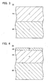
FIG. 2 is a cross-sectional view of asilicon wafer 30; -
FIG. 3 is a cross-sectional view of awafer 32 after a lowconcentration drift layer 16 is formed; -
FIG. 4 is a cross-sectional view of thewafer 32 after ananode layer 18 is formed; -
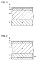
FIG. 5 is a cross-sectional view of thewafer 32 after a lower surface is polished; -
FIG. 6 is a cross-sectional view of thewafer 32 after acathode layer 12 is formed; -
FIG. 7 shows a schematic cross-sectional view of adiode 40 and a diagram depicting a distribution of a concentration Nd of impurities in each silicon layer; -
FIG. 8 is a cross-sectional view of awafer 52 after a second mediumconcentration drift layer 44b is formed; and -
FIG. 9 is a cross-sectional view of thewafer 52 after a lowconcentration drift layer 46 is formed. -
Fig. 1(a) shows a schematic cross-sectional view of adiode 10. AsFig. 1(a) shows, thediode 10 has acathode layer 12, a mediumconcentration drift layer 14, a lowconcentration drift layer 16 and ananode layer 18. Thecathode layer 12, the mediumconcentration drift layer 14 and the lowconcentration drift layer 16 are n-type silicon layers. Theanode layer 18 is a p-type silicon layer. The mediumconcentration drift layer 14 is formed on thecathode layer 12. The lowconcentration drift layer 16 is formed on the mediumconcentration drift layer 14. Theanode layer 18 is formed on the lowconcentration drift layer 16. Thediode 10 further has ananode electrode 22 formed on an upper surface of theanode layer 18, and acathode electrode 20 formed on a lower surface of thecathode layer 12. -
Fig. 1(b) shows a distribution of a concentration Nd of impurities in the silicon layers 12 to 18. InFig. 1(b) , the concentration of n-type impurities is shown for thecathode layer 12, the mediumconcentration drift layer 14 and the lowconcentration drift layer 16, and the concentration of p-type impurities is shown for theanode layer 18. AsFig. 1(b) shows, the concentration of n-type impurities in thecathode layer 12 is high, and thecathode layer 12 is connected to thecathode electrode 20 by ohmic connection. The concentration of n-type impurities in the mediumconcentration drift layer 14 is lower than that in thecathode layer 12. The concentration of n-type impurities in the lowconcentration drift layer 16 is lower than that in the mediumconcentration drift layer 14. The concentration of p-type impurities in theanode layer 18 is high, and theanode layer 18 is connected to theanode electrode 22 by ohmic connection. In the present embodiment, the concentration of n-type impurities in thecathode layer 12 is approximately 1 × 10¹⁹ atoms/cm3, the concentration of n-type impurities in the mediumconcentration drift layer 14 is approximately 1 × 10¹⁴ atoms/cm3, the concentration of n-type impurities in the lowconcentration drift layer 16 is approximately 7 × 10¹³ atoms/cm3, and the concentration of p-type impurities in theanode layer 18 is approximately 1 × 10¹⁹ atoms/cm3. - An operation of the
diode 10 upon reverse recovery will now be described. When thediode 10 is switched from a state where forward voltage is applied to a state where reverse voltage is applied, a depletion layer spreads in the lowconcentration drift layer 16 from a p-n junction at a boundary of the lowconcentration drift layer 16 and theanode layer 18. By the depletion layer spreading into the lowconcentration drift layer 16, carriers, which existed in the lowconcentration drift layer 16 while the forward voltage was applied, are exhausted. In other words, holes are exhausted to theanode electrode 22, and electrons are exhausted to thecathode electrode 20. Due to this, the reverse current flows through thediode 10. At this time, since the concentration of n-type impurities of the mediumconcentration drift layer 14 is relatively high, the depletion layer hardly spread in the mediumconcentration drift layer 14. Therefore, after the depletion layer spreads in the lowconcentration drift layer 16, the depletion layer then stops in the mediumconcentration drift layer 14. In other words, the spread of the depletion layer stops at a position indicated by the dottedline 90 inFig. 1 . As a consequence, the depletion layer does not spread into the mediumconcentration drift layer 14 in the portion lower than the dottedline 90, and carriers remain in the mediumconcentration drift layer 14 in a portion lower than the dottedline 90. Hence rapid exhaustion of carriers is suppressed. The reverse current attenuates as the exhaustion of carriers progresses. An induced electromotive force is generated by a parasitic inductor of thediode 10 when the reverse current attenuates. This induced electromotive force becomes the recovery surge voltage. The faster the attenuation speed of the reverse current is, the larger the recovery surge voltage is. In thediode 10, the attenuation speed of the reverse current is slow, since the rapid exhaustion of carriers is suppressed. Consequently, a high recovery surge voltage is hardly generated in thediode 10. - A method of manufacturing the
diode 10 will now be described. Thediode 10 is manufactured from asilicon wafer 30 shown inFig. 2 . Thesilicon wafer 30 is made of n-type silicon. A concentration of n-type impurities in thesilicon wafer 30 is approximately the same as the concentration of n-type impurities in the mediumconcentration drift layer 14. A thickness of thesilicon wafer 30 is approximately 600 µm. - First as
Fig. 3 shows, the lowconcentration drift layer 16 is grown on thesilicon wafer 30 by epitaxial growth. Here, the lowconcentration drift layer 16 is formed with an approximately 100 µm thickness. The lowconcentration drift layer 16 is formed so as to have a concentration of n-type impurities lower than that of thesilicon wafer 30. Hereafter thesilicon wafer 30 and the layers formed on the surface of the silicon wafer 30 (i.e., the lowconcentration drift layer 16 and various layers formed in the following steps) are collectively called a "wafer 32". - Then p-type impurities are injected to an upper surface of the low
concentration drift layer 16, and thewafer 32 is heat-treated. AsFig. 4 shows, due to this, a region near the upper surface of the lowconcentration drift layer 16 becomes p-type, and theanode layer 18 is formed. Then a withstand voltage structure, which is not illustrated, is formed on the upper surface of thewafer 32. Furthermore, theanode electrode 22 is formed on the upper surface of thewafer 32. - After the
anode electrode 22 is formed, the lower surface of thesilicon wafer 30 is polished so as to make thesilicon wafer 30 thinner, as shown inFig. 5 . Here the polishing is performed until the thickness of thesilicon wafer 30 becomes approximately 30 µm. - Then n-type impurities, such as arsenic and phosphorus, are injected to the lower surface of the
silicon wafer 30, and thewafer 32 is heat-treated. AsFig. 6 shows, due to this, a concentration of n-type impurities in a region near the lower surface of thesilicon wafer 30 increases, and thecathode layer 12 is formed. A region which is within thesilicon wafer 30 and did not become thecathode layer 12 becomes the mediumconcentration drift layer 14, in which a concentration of n-type impurities is lower than that in thecathode layer 12, and is higher than that in the lowconcentration drift layer 16. - Then the
cathode electrode 20 is formed on the lower surface of thewafer 32. Next, thewafer 32 is separated by dicing and thediode 10, shown inFig. 1(a) , is completed. - As described above, according to the method of manufacturing the
diode 10 of the first embodiment, only the lowconcentration drift layer 16 is grown by the epitaxial growth. Therefore the epitaxial growth does not require a long time. Since the layer grown by the epitaxial growth is not so thick, defects hardly occur. As a consequence, thediodes 10 can be manufactured efficiently. Furthermore, according to the manufacturing method of the first embodiment, the mediumconcentration drift layer 14 is formed using thesilicon wafer 30. Hence the mediumconcentration drift layer 14 having a sufficient thickness to suppress the recovery surge voltage can be formed. - Furthermore, according to the method of manufacturing the
diode 10 of the first embodiment, thecathode layer 12 is formed by ion injection, therefore the concentration of n-type impurities in thecathode layer 12 can be increased. As a result, contact resistance between thecathode layer 12 and thecathode electrode 20 can be decreased. - According to the first manufacturing method of Japanese Patent Application Laid-Open No.
2000-228404 silicon wafer 30 is not so high, hence arsenic need not be used for the n-type impurities in thesilicon wafer 30. If arsenic is not used, the above mentioned problems do not occur. Even if arsenic is used, the above mentioned problems hardly occur since the concentration of arsenic is low. - In the
diode 10 manufactured according to the above mentioned manufacturing method of the first embodiment, the mediumconcentration drift layer 14 is formed using thesilicon wafer 30. The manufacturing variation in the concentration of n-type impurities in thesilicon wafer 30 is large. Therefore the concentration of n-type impurities in the mediumconcentration drift layer 14 varies among thediodes 10 to be manufactured. Hence a manufacturing variation in the stop position of the depletion layer (that is, the position of the dottedline 90 inFig. 1(a) ) increases. As a result, the magnitude of the recovering surge voltage varies among the diodes to be manufactured. - The second embodiment provides a manufacturing method for suppressing the manufacturing variation in the recovery surge voltage. According to the manufacturing method of the second embodiment, a
diode 40 shown inFig. 7(a) is manufactured. AsFig. 7(a) shows, in thediode 40, a medium concentration drift layer is comprised of a first mediumconcentration drift layer 44a and a second mediumconcentration drift layer 44b. The rest of the configuration is the same as that of thediode 10 of the first embodiment. -
Fig. 7(b) shows a concentration Nd of impurities in silicon layers 42 to 48. InFig. 7(b) , the concentration of n-type impurities is shown for acathode layer 42, the first mediumconcentration drift layer 44a, the second mediumconcentration drift layer 44b, and a lowconcentration drift layer 46, and the concentration of p-type impurities is shown for ananode layer 48. AsFig. 7(b) shows, the concentrations of impurities in thecathode layer 42, the lowconcentration drift layer 46 and theanode layer 48 are approximately the same as those of thediode 10 of the first embodiment. The concentrations of n-type impurities in the first mediumconcentration drift layer 44a and the second mediumconcentration drift layer 44b are lower than that in thecathode layer 42, and higher than that in the lowconcentration drift layer 46. The concentration of n-type impurities in the second mediumconcentration drift layer 44b is higher than that in the first mediumconcentration drift layer 44a. In the present embodiment, the concentration of n-type impurities in thecathode layer 42 is approximately 1 × 10¹⁹ atoms/cm3, the concentration of n-type impurities in the first mediumconcentration drift layer 44a is approximately 1 × 10¹⁴ atoms/cm3, the concentration of n-type impurities in the second mediumconcentration drift layer 44b is approximately 5 × 10¹⁴ atoms/cm2, the concentration of n-type impurities in the lowconcentration drift layer 46 is approximately 6 × 10¹³ atoms/cm2, and the concentration of p-type impurities in theanode layer 48 is approximately 1 × 10¹⁹ atoms/cm2. - The thicknesses of the low
concentration drift layer 46 and the second mediumconcentration drift layer 44b described above are set so that a depletion layer stops in the second mediumconcentration drift layer 44b when reverse voltage is applied to thediode 40. Specifically, the thicknesses are set such that the following relational expression is satisfied.
Here, a symbol Wd1 denotes the thickness of the lowconcentration drift layer 46, a symbol Wd2 denotes the thickness of the second mediumconcentration drift layer 44b, a symbol ε0 denotes a permittivity in a vacuum, a symbol εSi denotes a relative permittivity of the lowconcentration drift layer 46 and the second mediumconcentration drift layer 44b (relative permittivity of silicon in this embodiment), a symbol Va denotes a rated voltage of the diode 40 (reverse voltage applied when thediode 40 is used), a symbol q denotes an elementary charge, and a symbol Nd0 denotes an average value of the concentrations ofn-type impurities of the lowconcentration drift layer 46 and the second mediumconcentration drift layer 44b. The average impurity concentration Nd0 is given by the following expression.
Here, a symbol Nd1 denotes a concentration of n-type impurities in the lowconcentration drift layer 46, and a symbol Nd2 denotes a concentration of n-type impurities in the second mediumconcentration drift layer 44b. - As described in detail later, since the first medium
concentration drift layer 44a is formed of a silicon wafer, the manufacturing variation in the concentration of n-type impurities in the first mediumconcentration drift layer 44a is large. On the other hand, since the second mediumconcentration drift layer 44b is an epitaxial layer, the manufacturing variation in the concentration of n-type impurities in the second mediumconcentration drift layer 44b is very small. - An operation of the
diode 40 upon reverse recovery will now be described. When thediode 40 is switched from a state where forward voltage is applied to a state where reverse voltage is applied, a depletion layer spreads into the lowconcentration drift layer 46 from a p-n junction at a boundary of the lowconcentration drift layer 46 and theanode layer 48. The spread of the depletion layer stops in the second mediumconcentration drift layer 44b. In other words, the spread of the depletion layer stops at a position indicated by the dottedline 92 inFig. 7(a) . As a consequence, the depletion layer does not spread into the first mediumconcentration drift layer 44a, and carriers remain in the first mediumconcentration drift layer 44a. Consequently, high recovery surge voltage is hardly generated in thediode 40. - As mentioned above, the second medium
concentration drift layer 44b is an epitaxial layer, therefore the manufacturing variation in the concentration of n-type impurities in the second mediumconcentration drift layer 44b is not large. As a consequence, the manufacturing variation in the stop position of the depletion layer indicated by the dottedline 92 hardly occurs. Hence in thediode 40, the manufacturing variation in the magnitude of the recovery surge voltage is suppressed. - A method of manufacturing the
diode 40 will now be described. Just like thediode 10 of the first embodiment, thediode 40 is manufactured from thesilicon wafer 30 shown inFig. 2 . - First as
Fig. 8 shows, the second mediumconcentration drift layer 44b is grown on thesilicon wafer 30 by epitaxial growth. Here the second mediumconcentration drift layer 44b is formed with an approximately 10 µm thickness. Furthermore, the second mediumconcentration drift layer 44b is formed so as to have a concentration of n-type impurities that is higher than that in thesilicon wafer 30. Hereafter thesilicon wafer 30 and the layers formed on the surface of the silicon wafer 30 (i.e., the second mediumconcentration drift layer 44b and various layers formed in the following steps) are collectively called a "wafer 52". - Then, as
Fig. 9 shows, the lowconcentration drift layer 46 is grown on the second mediumconcentration drift layer 44b by epitaxial growth. Here the lowconcentration drift layer 46 is formed with an approximately 90 µm thickness. Furthermore, the lowconcentration drift layer 46 is formed so as to have a concentration of n-type impurities lower than that in thesilicon wafer 30. - Then, just like the first embodiment, the
anode layer 48 is formed, theanode electrode 22 is formed, the lower surface of thesilicon wafer 30 is polished, thecathode layer 42 is formed, and thecathode electrode 20 is formed. A region which is within thesilicon wafer 30 and did not become thecathode layer 42 becomes the first mediumconcentration drift layer 44a. Next, thewafer 52 is separated by dicing and thediode 40, shown inFig. 7(a) , is completed. - As described above, according to the method of manufacturing the
diode 40 of the second embodiment, the second mediumconcentration drift layer 44b is formed by epitaxial growth. The epitaxial growth can accurately control the concentration of n-type impurities in the second mediumconcentration drift layer 44b. Hence the variation in the stop position of the depletion layer, when the reverse voltage is applied to the diode 40 (that is, the position of the dottedline 92 inFig. 7(a) ), hardly occur. According to the manufacturing method of the second embodiment, thediodes 40, among which recovery surge voltage does not vary much, can be manufactured. As a result of a simulation performed for verifying a variation range of the recovery surge voltage generated due to the manufacturing variation in the concentration of n-type impurities in thesilicon wafer 30, the variation range of the recovery surge voltage in thediodes 10 of the first embodiment is 152 V, while the variation range of the recovery surge voltage in thediodes 40 of the second embodiment is 43 V. Furthermore, by suppressing the variation in the stopping position of the depletion layer, variation in the withstand characteristics for reverse voltage among thediodes 40 is also decreased. As a result of a simulation performed for verifying a variation range of the withstand voltage due to the manufacturing variation in the concentration of n-type impurities in thesilicon wafer 30, a variation range of the withstand voltage in thediodes 10 of the first embodiment is 207 V, while the variation range of the withstand voltage in thediodes 40 of the second embodiment is 126 V. Thus according to the manufacturing method of the second embodiment, even if the concentration of n-type impurities in thesilicon wafer 30 varies,diodes 40 having stable characteristics can be manufactured. - According to the manufacturing method of the second embodiment, the first medium
concentration drift layer 44a is formed of thesilicon wafer 30, and the lowconcentration drift layer 46 and the second mediumconcentration drift layer 44b are formed by the epitaxial growth. Since the layer to be formed by the epitaxial growth is not so thick, the manufacturing method of the second embodiment allows manufacturing thediodes 40 efficiently. In the case of the manufacturing method of the second embodiment also, the problem of arsenic does not occur, just like the manufacturing method of the first embodiment. - Note that in the case of the above mentioned
diode 40 of the second embodiment, the concentration of n-type impurities in the second mediumconcentration drift layer 44b is higher than that in the first mediumconcentration drift layer 44a. In order to stop the depletion layer, the higher concentration of n-type impurities in the second mediumconcentration drift layer 44b is preferable. However, if the depletion layer can be stopped in the second mediumconcentration drift layer 44b, the concentration of n-type impurities in the second mediumconcentration drift layer 44b may be lower than that in the first mediumconcentration drift layer 44a. With this configuration as well, the effect of decreasing the variation in the recovery surge voltage can be obtained if the second mediumconcentration drift layer 44b is an epitaxial layer. In other words, it is sufficient if an epitaxial layer, for stopping the spread of the depletion layer upon applying reverse voltage, is formed in the drift layer. - The technical elements described in the present specification and the drawings exhibit technical utility individually or by various combinations thereof, and are not limited to the combinations stated in the Claims in the application. The technology described in the present specification or the drawings is for achieving a plurality of purposes simultaneously, and has technical utility by achieving one of these purposes.
Claims (4)
- A method of manufacturing a diode, the diode including a high concentration n-type semiconductor layer; a medium concentration n-type semiconductor layer formed on the high concentration n-type semiconductor layer; a low concentration n-type semiconductor layer formed on the medium concentration n-type semiconductor layer, and a p-type semiconductor layer formed on the low concentration n-type semiconductor layer,
the method comprising:growing the low concentration n-type semiconductor layer on an n-type semiconductor substrate by epitaxial growth, wherein a concentration of n-type impurities in the low concentration n-type semiconductor layer is lower than that in the n-type semiconductor substrate; andforming the high concentration n-type semiconductor layer by injecting n-type impurities to a lower surface of the n-type semiconductor substrate. - A method of manufacturing a diode, the diode including a high concentration n-type semiconductor layer; a first medium concentration n-type semiconductor layer formed on the high concentration n-type semiconductor layer; a second medium concentration n-type semiconductor layer formed on the first medium concentration n-type semiconductor layer; a low concentration n-type semiconductor layer formed on the second medium concentration n-type semiconductor layer; and a p-type semiconductor layer formed on the low concentration n-type semiconductor layer,
the method comprising:growing the second medium concentration n-type semiconductor layer on an n-type semiconductor substrate by epitaxial growth;growing the low concentration n-type semiconductor layer on the second medium concentration n-type semiconductor layer by epitaxial growth, wherein a concentration of n-type impurities in the low concentration n-type semiconductor layer is lower than those in the n-type semiconductor substrate and the second medium concentration n-type semiconductor layer; andforming the high concentration n-type semiconductor layer by injecting n-type impurities to a lower surface of the n-type semiconductor substrate, wherein a concentration of n-type impurities in the high concentration n-type semiconductor layer is higher than that in the second medium concentration n-type semiconductor layer. - The method of manufacturing the diode as in claim 2, wherein the second medium concentration n-type semiconductor layer, in which the concentration of n-type impurities is higher than that in the n-type semiconductor substrate, is formed.
- A diode comprising:a high concentration n-type semiconductor layer;a first medium concentration n-type semiconductor layer formed on the high concentration n-type semiconductor layer,a second medium concentration n-type semiconductor layer formed on the first medium concentration n-type semiconductor layer;a low concentration n-type semiconductor layer formed on the second medium concentration n-type semiconductor layer; anda p-type semiconductor layer formed on the low concentration n-type semiconductor layer,wherein a concentration NH of n-type impurities in the high concentration n-type semiconductor layer, a concentration NM1 of n-type impurities in the first medium concentration n-type semiconductor layer, a concentration NM2 of n-type impurities in the second medium concentration n-type semiconductor layer, and a concentration NL of n-type impurities in the low concentration n-type semiconductor layer satisfy a relationship of NL<NM1<NM2<NH.
Applications Claiming Priority (1)
| Application Number | Priority Date | Filing Date | Title |
|---|---|---|---|
| PCT/JP2009/059759 WO2010137146A1 (en) | 2009-05-28 | 2009-05-28 | Method for producing diode, and diode |
Publications (2)
| Publication Number | Publication Date |
|---|---|
| EP2437287A1 true EP2437287A1 (en) | 2012-04-04 |
| EP2437287A4 EP2437287A4 (en) | 2014-03-19 |
Family
ID=43222287
Family Applications (1)
| Application Number | Title | Priority Date | Filing Date |
|---|---|---|---|
| EP09845213.9A Withdrawn EP2437287A4 (en) | 2009-05-28 | 2009-05-28 | METHOD FOR PRODUCING DIODE, AND DIODE |
Country Status (6)
| Country | Link |
|---|---|
| US (1) | US20120007222A1 (en) |
| EP (1) | EP2437287A4 (en) |
| JP (1) | JP5282818B2 (en) |
| KR (1) | KR101288263B1 (en) |
| CN (1) | CN102414805B (en) |
| WO (1) | WO2010137146A1 (en) |
Families Citing this family (8)
| Publication number | Priority date | Publication date | Assignee | Title |
|---|---|---|---|---|
| JP5872327B2 (en) * | 2011-03-10 | 2016-03-01 | 株式会社東芝 | Semiconductor rectifier |
| WO2012136848A1 (en) | 2011-04-06 | 2012-10-11 | Abb Technology Ag | Bipolar punch-through semiconductor device and method for manufacturing such a semiconductor device |
| JP6098540B2 (en) * | 2014-02-10 | 2017-03-22 | トヨタ自動車株式会社 | Semiconductor device and manufacturing method of semiconductor device |
| CN107123689A (en) * | 2017-03-22 | 2017-09-01 | 中航(重庆)微电子有限公司 | A kind of high pressure PIN diode structure and preparation method thereof |
| CN107507870A (en) * | 2017-07-06 | 2017-12-22 | 全球能源互联网研究院有限公司 | Diode |
| WO2020229402A1 (en) * | 2019-05-10 | 2020-11-19 | Abb Power Grids Switzerland Ag | A dual base thin wafer power semiconductor device and method for manufacturing the same |
| DE102020118404A1 (en) | 2020-07-13 | 2022-01-13 | Infineon Technologies Ag | VERTICAL POWER SEMICONDUCTOR DEVICE AND METHOD OF MANUFACTURE |
| CN115472668A (en) * | 2022-05-05 | 2022-12-13 | 安世半导体科技(上海)有限公司 | Semiconductor device and method for manufacturing the same |
Family Cites Families (13)
| Publication number | Priority date | Publication date | Assignee | Title |
|---|---|---|---|---|
| JPS58216473A (en) * | 1982-06-11 | 1983-12-16 | Hitachi Ltd | Diode |
| JP3353277B2 (en) * | 1992-09-25 | 2002-12-03 | ソニー株式会社 | Manufacturing method of epitaxial wafer |
| JP2000223720A (en) * | 1999-01-29 | 2000-08-11 | Meidensha Corp | Semiconductor element and life time control method |
| JP2000228404A (en) * | 1999-02-05 | 2000-08-15 | Hitachi Ltd | diode |
| JP3951738B2 (en) * | 2001-02-23 | 2007-08-01 | 富士電機デバイステクノロジー株式会社 | Manufacturing method of semiconductor device |
| DE10207522B4 (en) * | 2001-02-23 | 2018-08-02 | Fuji Electric Co., Ltd. | Semiconductor component and method for its production |
| JP4539011B2 (en) * | 2002-02-20 | 2010-09-08 | 富士電機システムズ株式会社 | Semiconductor device |
| JP4000927B2 (en) * | 2002-07-03 | 2007-10-31 | 富士電機デバイステクノロジー株式会社 | Semiconductor device and manufacturing method thereof |
| JP2005079232A (en) * | 2003-08-29 | 2005-03-24 | Shindengen Electric Mfg Co Ltd | High speed switching diode and manufacturing method thereof |
| JP2006049473A (en) * | 2004-08-03 | 2006-02-16 | Toyota Central Res & Dev Lab Inc | Vertical semiconductor device |
| JP2006245475A (en) * | 2005-03-07 | 2006-09-14 | Toshiba Corp | Semiconductor device and manufacturing method thereof |
| DE102005046707B3 (en) * | 2005-09-29 | 2007-05-03 | Siced Electronics Development Gmbh & Co. Kg | SiC-PN power diode |
| JP5272299B2 (en) * | 2005-11-10 | 2013-08-28 | 富士電機株式会社 | Semiconductor device and manufacturing method thereof |
-
2009
- 2009-05-28 WO PCT/JP2009/059759 patent/WO2010137146A1/en not_active Ceased
- 2009-05-28 EP EP09845213.9A patent/EP2437287A4/en not_active Withdrawn
- 2009-05-28 JP JP2011515802A patent/JP5282818B2/en not_active Expired - Fee Related
- 2009-05-28 KR KR1020117023248A patent/KR101288263B1/en not_active Expired - Fee Related
- 2009-05-28 CN CN200980159078.5A patent/CN102414805B/en not_active Expired - Fee Related
-
2011
- 2011-09-23 US US13/241,429 patent/US20120007222A1/en not_active Abandoned
Also Published As
| Publication number | Publication date |
|---|---|
| US20120007222A1 (en) | 2012-01-12 |
| CN102414805A (en) | 2012-04-11 |
| JPWO2010137146A1 (en) | 2012-11-12 |
| KR101288263B1 (en) | 2013-07-26 |
| KR20110137338A (en) | 2011-12-22 |
| EP2437287A4 (en) | 2014-03-19 |
| JP5282818B2 (en) | 2013-09-04 |
| WO2010137146A1 (en) | 2010-12-02 |
| CN102414805B (en) | 2014-04-23 |
Similar Documents
| Publication | Publication Date | Title |
|---|---|---|
| EP2437287A1 (en) | Method for producing diode, and diode | |
| EP1806787B1 (en) | Silicon carbide bipolar transistor and method of fabricating thereof | |
| EP1438739B1 (en) | Sic bipolar semiconductor devices with few crystal defects | |
| US7646061B2 (en) | Power semiconductor component with charge compensation structure and method for producing the same | |
| US8163630B2 (en) | Method of manufacturing a semiconductor device | |
| JP5411422B2 (en) | Bipolar semiconductor device, method for manufacturing the same, and method for controlling zener voltage | |
| EP2525410A1 (en) | Insulated gate bipolar transistor and manufacturing method thereof | |
| US8569150B2 (en) | Method for producing a semiconductor device with a semiconductor body | |
| DE102019106124A1 (en) | Forming semiconductor devices in silicon carbide | |
| CN102820225B (en) | There is the manufacture method of the high-voltage high-speed soft-recovery diode of diffusing buffer layer | |
| CN108110081A (en) | Novel heterojunction avalanche photodide | |
| CN105895679A (en) | Structure and manufacturing method of insulated gate bipolar transistor | |
| EP2080222B1 (en) | Method of forming a semiconductor wafer suitable for forming a semiconductor p/n junction diode | |
| US20240234515A9 (en) | Silicon carbide wafer and silicon carbide semiconductor device including the same | |
| US20200350408A1 (en) | Stacked high barrier iii-v power semiconductor diode | |
| CN121099620A (en) | Semiconductor structure and manufacturing method thereof | |
| US20230086715A1 (en) | Stacked diode with side passivation and method of making the same | |
| JPH0846221A (en) | Semiconductor device and manufacturing method thereof | |
| JP3970729B2 (en) | Semiconductor device and manufacturing method thereof | |
| US20240120423A1 (en) | Semiconductor device | |
| JP7266761B2 (en) | A semiconductor device that gradually injects charge carriers for slower reverse recovery | |
| CN121357912A (en) | Fast recovery diode and preparation method thereof | |
| CN116897434A (en) | Silicon carbide semiconductor device and silicon carbide semiconductor substrate | |
| CN118173581A (en) | III-V semiconductor super junction device and manufacturing method thereof | |
| CN103050397A (en) | Process implementation method of epitaxial field barrier layer at back of IGBT (Insulated Gate Bipolar Translator) device |
Legal Events
| Date | Code | Title | Description |
|---|---|---|---|
| PUAI | Public reference made under article 153(3) epc to a published international application that has entered the european phase |
Free format text: ORIGINAL CODE: 0009012 |
|
| 17P | Request for examination filed |
Effective date: 20110721 |
|
| AK | Designated contracting states |
Kind code of ref document: A1 Designated state(s): AT BE BG CH CY CZ DE DK EE ES FI FR GB GR HR HU IE IS IT LI LT LU LV MC MK MT NL NO PL PT RO SE SI SK TR |
|
| DAX | Request for extension of the european patent (deleted) | ||
| RAP1 | Party data changed (applicant data changed or rights of an application transferred) |
Owner name: TOYOTA JIDOSHA KABUSHIKI KAISHA |
|
| A4 | Supplementary search report drawn up and despatched |
Effective date: 20140217 |
|
| RIC1 | Information provided on ipc code assigned before grant |
Ipc: H01L 29/36 20060101ALI20140211BHEP Ipc: H01L 21/329 20060101AFI20140211BHEP Ipc: H01L 29/861 20060101ALI20140211BHEP |
|
| STAA | Information on the status of an ep patent application or granted ep patent |
Free format text: STATUS: THE APPLICATION IS DEEMED TO BE WITHDRAWN |
|
| 18D | Application deemed to be withdrawn |
Effective date: 20140917 |