JP3970729B2 - Semiconductor device and manufacturing method thereof - Google Patents
Semiconductor device and manufacturing method thereof Download PDFInfo
- Publication number
- JP3970729B2 JP3970729B2 JP2002275389A JP2002275389A JP3970729B2 JP 3970729 B2 JP3970729 B2 JP 3970729B2 JP 2002275389 A JP2002275389 A JP 2002275389A JP 2002275389 A JP2002275389 A JP 2002275389A JP 3970729 B2 JP3970729 B2 JP 3970729B2
- Authority
- JP
- Japan
- Prior art keywords
- film
- silicon
- silicon germanium
- germanium film
- conductivity type
- Prior art date
- Legal status (The legal status is an assumption and is not a legal conclusion. Google has not performed a legal analysis and makes no representation as to the accuracy of the status listed.)
- Expired - Fee Related
Links
Images


Description
【0001】
【発明の属する技術分野】
本発明は、半導体装置およびその製造技術に関し、特に、PIN(Positive Intrinsic Negative)ダイオードを有する半導体装置に適用して有効な技術に関する。
【0002】
【従来の技術】
PINダイオードは、例えば、相対的に高濃度にドープされたn型の導電性を示す半導体基板(N層)上に、相対的に低濃度にドープされたn型エピタキシャルシリコン膜(I層)を成長させ、熱酸化処理などによりエピタキシャルシリコン膜の表面にシリコン酸化膜を形成した後、シリコン酸化膜の一部を取り除いて開口部を形成し、続いてその開口部を通じてp型の導電性を示す不純物をエピタキシャルシリコン膜へ拡散してp型半導体領域(P層)を形成することにより、形成される。
【0003】
【発明が解決しようとする課題】
近年、PINダイオードの低電流駆動化が要求されてきている。上記構造のPINダイオードでは、PINダイオードを構成するP層、I層およびN層のいずれもシリコン層を用いているため、各層のバンドギャップは一様(約1.1eV)であり、I層の抵抗値を変える場合には、このエネルギーギャップ以上の電圧をP層とN層の間に印加してキャリアをI層に注入しなければI層の抵抗値を変化させることができない。従って、PINダイオードのオン抵抗の低減には、限界がある。
【0004】
本発明の目的は、低オン抵抗化が可能なダイオードを有する半導体装置およびその製造方法を提供することにある。
【0005】
本発明の前記ならびにその他の目的と新規な特徴は、本明細書の記述および添付図面から明らかになるであろう。
【0006】
【課題を解決するための手段】
本願において開示される発明のうち、代表的なものの概要を簡単に説明すれば、次のとおりである。
【0007】
本発明の半導体装置は、第1導電型の半導体基板と、半導体基板上に形成された第1導電型の第1シリコンゲルマニウム膜と、第1シリコンゲルマニウム膜上に形成された第1導電型の第2シリコンゲルマニウム膜と、第2シリコンゲルマニウム膜上に形成された第1導電型のシリコン膜と、シリコン膜の上面側に形成された第1導電型と逆の第2導電型の半導体領域とを有し、第2シリコンゲルマニウム膜のゲルマニウム濃度が第1シリコンゲルマニウム膜との界面からシリコン膜との界面に向かって徐々に減少しているものである。
【0008】
また、本発明の半導体装置の製造方法は、第1導電型の半導体基板を準備する工程と、半導体基板上に第1導電型の第1シリコンゲルマニウム膜をエピタキシャル成長させる工程と、第1シリコンゲルマニウム膜上に第1導電型の第2シリコンゲルマニウム膜をエピタキシャル成長させる工程と、第2シリコンゲルマニウム膜上に第1導電型のシリコン膜をエピタキシャル成長させる工程と、シリコン膜の上面側に第1導電型と逆の第2導電型の半導体領域を形成する工程とを有し、第2シリコンゲルマニウム膜のゲルマニウム濃度が第1シリコンゲルマニウム膜との界面からシリコン膜との界面に向かって徐々に減少しているものである。
【0009】
【発明の実施の形態】
以下、本発明の実施の形態を図面に基づいて詳細に説明する。なお、実施の形態を説明するための全図において、同一の機能を有する部材には同一の符号を付し、その繰り返しの説明は省略する。また、以下の実施の形態では、特に必要なとき以外は同一または同様な部分の説明を原則として繰り返さない。
【0010】
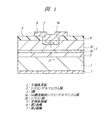
本実施の形態の半導体装置を図面を参照して説明する。図1は、本発明の一実施の形態である半導体装置、例えばPIN(Positive Intrinsic Negative)ダイオードの要部断面図である。
【0011】
図1に示されるように、比較的または相対的に高い不純物濃度(例えば1019〜1020個/cm3程度)を有するn型(n+型)シリコンからなる半導体基板1上に、相対的に高い不純物濃度を有するn型(n+型)のシリコンゲルマニウム(SiGe)膜2と、相対的に低い不純物濃度(例えば1013〜1016個/cm3程度)を有するn型(n-型)のI(Intrinsic)層3とが形成(エピタキシャル成長)されている。半導体基板1、シリコンゲルマニウム膜2およびI層3には、n型の導電型を有する不純物、例えばP(リン)またはAs(ヒ素)がドーピングまたは導入されている。半導体基板1の厚みは例えば100μm程度であり、シリコンゲルマニウム膜2の厚みは例えば0.5〜2μm程度であり、I層3の厚みは例えば20μm程度である。シリコンゲルマニウム膜2のゲルマニウム濃度(濃度分布)は、場所によらず膜内でほぼ一定または均一であり、例えば15原子%(従ってシリコン濃度は85原子%)である。
【0012】
I層3は、シリコンゲルマニウム膜2上のGe濃度傾斜シリコンゲルマニウム膜(シリコンゲルマニウム領域)3aと、その上のゲルマニウムを含有していないシリコン膜(シリコン領域)3bとからなる。Ge濃度傾斜シリコンゲルマニウム膜3a内のゲルマニウム濃度は、シリコンゲルマニウム膜2との界面からシリコン膜3bとの界面に向かって徐々に減少している。すなわち、Ge濃度傾斜シリコンゲルマニウム膜3aの厚み方向のゲルマニウム濃度分布は、シリコンゲルマニウム膜2との界面からシリコン膜3bとの界面に向かって徐々に減少している。
【0013】
I層3上には、例えば酸化シリコンなどからなり、開口部4aを有する絶縁膜4が形成されている。開口部4aから露出するI層3(シリコン膜3b)には所定の深さ(例えば2〜3μm程度)までp型の導電型を有する不純物(例えばB(ボロン))が拡散され、相対的に高い不純物濃度(例えば1019〜1020個/cm3程度)を有するp型(p+型)の半導体領域(不純物拡散領域)5が形成されている。更に、開口部4aから露出する半導体領域5上には第1電極(表面電極)6が形成され、半導体基板1の裏面上には第2電極(裏面電極)7が形成されている。
【0014】
第1電極6と第2電極7の間には、半導体基板1(N層)、シリコンゲルマニウム膜2、I層3、および半導体領域5(P層)によってPINダイオードが形成され、第1電極6と第2電極7との間に所定の電圧を印加することで、PINダイオードを作動させることができる。
【0015】
図2は、図1の半導体装置のA―A線に沿った(厚み方向の)シリコン濃度およびゲルマニウム濃度分布を示すグラフである。図2のグラフの横軸が、厚み方向(半導体基板1の主面に垂直な方向)の距離または位置(任意単位:arbitrary unit)に対応し、図2のグラフの縦軸がゲルマニウム濃度(Ge濃度)およびシリコン濃度(Si濃度)に対応する。
【0016】
図2に示されるように、シリコンゲルマニウム膜2の厚み方向(半導体基板1の主面に垂直な方向)のゲルマニウム濃度分布は一定(例えば15原子%)である。また、上記のように、I層3は、Ge濃度傾斜シリコンゲルマニウム膜3aとシリコン膜3bとからなるが、Ge濃度傾斜シリコンゲルマニウム膜3aの厚み方向(半導体基板1の主面に垂直な方向)のゲルマニウム濃度分布は、シリコンゲルマニウム膜2との界面での15原子%からシリコン膜3b側に向かって徐々に(なだらかに)減少し、シリコン膜3bとの界面でゼロになる。半導体基板1、I層3のシリコン膜3b、および半導体領域5は、ゲルマニウムを含有していない(すなわちシリコンからなる)。
【0017】
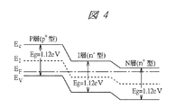
図3は、図1に示される半導体装置(PINダイオード)のA―A線に沿った領域のエネルギーバンド構造図である。図3のグラフの横軸が、各膜の厚み方向(半導体基板1の主面に垂直な方向)の距離または位置(任意単位:arbitrary unit)に対応し、図3のグラフの縦軸がエネルギーバンドに対応する。また、図4は、図1の構造においてシリコンゲルマニウム膜2およびGe濃度傾斜シリコンゲルマニウム膜3aを形成しなかった場合のエネルギーバンド構造図であり、図5は、図1の構造においてGe濃度傾斜シリコンゲルマニウム膜3aを形成しなかった場合のエネルギーバンド構造図である。図3〜図5のバンド構造図では、伝導帯下端のエネルギー準位EC、価電子帯上端のエネルギー準位EV、フェルミ準位EF、および真性(intrinsic)準位EIが記載されている。
【0018】
半導体基板1、シリコン膜3bおよびp型半導体領域5は、いずれもシリコンからなり、そのバンドギャップEgは約1.1eV(1.12eV)である。従って、PINダイオードが半導体基板1(N層)、シリコン膜3b(I層)およびp型半導体領域5(P層)により構成される場合は、エネルギーバンド構造は図4のようになる。
【0019】
また、ゲルマニウム濃度が約15原子%のシリコンゲルマニウム膜2のエネルギーギャップEgは、約1.0eVである。従って、PINダイオードが半導体基板1(N層)、シリコンゲルマニウム膜2(SiGe膜)、シリコン膜3b(I層)およびp型半導体領域5(P層)により構成される場合は、エネルギーバンド構造は図5のようになる。この場合、半導体基板1とシリコンゲルマニウム膜2との間の界面のギャップ差約0.1eVと、シリコンゲルマニウム膜2とシリコン膜3bとの間の界面のギャップ差約−0.1eVとは、半導体基板1からシリコン膜3bに注入される電子にとっては相殺されるので、PINダイオードのオン抵抗は図4の場合と図5の場合とで実質的に同じになる。
【0020】
それに対して、本実施の形態では、半導体基板1とシリコン膜3bとの間には、シリコンゲルマニウム膜2およびGe濃度傾斜シリコンゲルマニウム膜3aが形成されている。シリコンゲルマニウム膜のエネルギーギャップEgはゲルマニウム濃度に依存して変化し、ゲルマニウム濃度が小さくなるほどエネルギーギャップEgは大きくなる。従って、Ge濃度傾斜シリコンゲルマニウム膜3aのエネルギーギャップEgは、ゲルマニウム濃度が最大であるシリコンゲルマニウム膜2との界面では約1.0eVであり、そこから徐々に増大してシリコン膜3bとの界面では約1.1eV(1.12eV)となる。従って、PINダイオードが半導体基板1(N層)、シリコンゲルマニウム膜2(SiGe膜)、Ge濃度傾斜シリコンゲルマニウム膜3aおよびシリコン膜3b(I層)、およびp型半導体領域5(P層)により構成される本実施の形態の場合は、エネルギーバンド構造は図3のようになる。
【0021】
本実施の形態では、I層3をGe濃度傾斜シリコンゲルマニウム膜3aとシリコン膜3bとによって構成している。Ge濃度傾斜シリコンゲルマニウム膜3aを設けることにより、シリコンゲルマニウム膜2からI層3の内部にかけてゲルマニウム濃度をなだらかに連続的に減少させている。従って、シリコンゲルマニウム膜2とI層3との間(すなわちシリコンゲルマニウム膜2とシリコン膜3bとの間)のエネルギーギャップ差の傾斜が、図5の場合に比較してなだらかになり、シリコンゲルマニウム膜2とI層3との間でのエネルギーギャップ差を見かけ上ない(インピーダンス変換)構造とすることができる。このような構造においては、第1電極7aと第2電極8との間に電圧が印加された場合、半導体基板1に対して0.1eVのエネルギーギャップ差をもつシリコンゲルマニウム膜2では、図4の場合と比較して、0.1eV高い電圧が印加されたこととなり、その分電子の放出量が増加し、シリコン膜3b側へ加速される。更に、I層3ではGe濃度傾斜シリコンゲルマニウム膜3aを設けてゲルマニウム濃度をなだらかに減少させているため、図5の場合と比較して、シリコンゲルマニウム膜2とシリコン膜3bとの間のエネルギーギャップ差の傾斜が小さくなり(エネルギー勾配がゆるやかになり)、半導体基板1とシリコンゲルマニウム膜2との間で得た0.1eVのエネルギーにより余分に加速されたキャリア(電子)を消滅させることなくI層3(シリコン膜3b)に注入することが可能となる。I層3は真性半導体に近いため、一旦I層3(シリコン膜3b)内に到達した電子はキャリアとして存在し、PINダイオードのオン抵抗の低下に寄与する。また、キャリアとしての電子に対し、I層3(シリコン膜3b)内のマイナス電位が持ち上がるため、これを補償またはコンペンセイトするようなホール(正孔)の引き込みが発生し、更にI層3(シリコン膜3b)内をキャリアで充満することができる。これにより、更にオン抵抗を低減できる。また、I層3(シリコン膜3b)中のキャリア密度(単位体積当たりのキャリア)を増大させることが可能になる。また、PINダイオードを低オン抵抗に設計できるので、半導体装置の低消費電力化が可能となる。
【0022】
次に、本実施の形態の半導体装置の製造工程を図面を参照して説明する。図6〜図11は、本実施の形態の半導体装置、例えばPINダイオードの製造工程中の要部断面図である。
【0023】
図6に示されるように、n型の導電型を有する不純物(例えばP(リン)またはAs(ヒ素))が高濃度(例えば1019〜1020個/cm3程度)にドーピングされたn型シリコンからなる半導体基板1を用意する。半導体基板1はPINダイオードのN層として機能する。
【0024】
次に、図7に示されるように、半導体基板1上に、シリコンゲルマニウム膜2およびI(Intrinsic)層3を形成する。シリコンゲルマニウム膜2の厚みは例えば0.5〜2μm程度であり、I層3の厚みは例えば20μm程度である。シリコンゲルマニウム膜2およびI層3は、例えば次のようにして成膜される。
【0025】
キャリアガスとして例えば水素ガス(H2)、シリコンソースガスとして例えばモノシラン(SiH4)ガス、n型ドーピングガスとして例えばホスフィン(PH3)ガス、およびゲルマニウムソースガスとして例えばモノゲルマン(GeH4)ガスを成膜装置(例えばCVD装置)の処理室(反応室またはチャンバ)内に導入しながら、半導体基板1上にシリコンゲルマニウム膜2をエピタキシャル成長させる。この段階では、半導体基板1上には、比較的または相対的に高い不純物濃度のシリコンゲルマニウム膜2が形成される。シリコンゲルマニウム膜2の成膜段階では、成膜装置の処理室に導入するモノゲルマン(GeH4)ガスの流量を一定にする。このため、シリコンゲルマニウム膜2のゲルマニウム濃度(濃度分布)はほぼ一定または均一となる。
【0026】
所定の厚みのシリコンゲルマニウム膜2が形成された後、シリコンゲルマニウム膜2上に相対的に低い不純物濃度の半導体層すなわちI層3をエピタキシャル成長させるために、ホスフィンガスの成膜装置の処理室への導入を停止または減少させる。この際、モノゲルマンガスの流量を徐々に(なだらかに)減少させる(水素ガスとモノシランガスの導入は継続する)。これにより、シリコンゲルマニウム膜2上には、モノゲルマンガスの流量減少に応じて、ゲルマニウム濃度が徐々に(なだらかに)減少する比較的低不純物濃度のシリコンゲルマニウム膜、すなわちGe濃度傾斜シリコンゲルマニウム膜3aがエピタキシャル成長する。更に、モノゲルマン(GeH4)ガスの流量がゼロになった後も成膜を継続して、ゲルマニウムを含有しないシリコン膜3bをGe濃度傾斜シリコンゲルマニウム膜3a上にエピタキシャル成長させる。
【0027】
このようにして、半導体基板1上に、一定または均一のゲルマニウム濃度を有し高不純物濃度のシリコンゲルマニウム膜2、および、ゲルマニウム濃度が(厚み方向に)徐々に減少するGe濃度傾斜シリコンゲルマニウム膜3aとゲルマニウムを含まないシリコン膜3bとからなる低不純物濃度(例えば1013〜1016個/cm3程度)のI層3が連続的に(同一工程で)形成される。I層3はPINダイオードのI層として機能する。なお、半導体基板1上にエピタキシャル成長した膜を、ゲルマニウム濃度などによりシリコンゲルマニウム膜2、Ge濃度傾斜シリコンゲルマニウム膜3a、およびシリコン膜3bに分けているが、これらの膜は連続的にエピタキシャル成長しており、各膜の間に明確な界面が観測されない場合であっても、本実施の形態の構造に含まれるものとする。
【0028】
次に、図8に示されるように、I層3(シリコン膜3b)上に例えば酸化シリコン膜などからなる絶縁膜4を形成する。絶縁膜4は、例えば熱酸化処理などにより形成することができる。それから、フォトリソグラフィ技術によりパターニングされたフォトレジスト膜(図示は省略)をマスクとして絶縁膜4をエッチングし、I層3に達する開口部4aを形成する。
【0029】
次に、上記フォトレジスト膜を除去した後、図9に示されるように、開口部4aから露出したI層3に、p型の導電型を有する不純物(例えばB(ボロン))をイオン注入し、必要に応じて熱処理を行うことで、相対的に高い不純物濃度(例えば1019〜1020個/cm3程度)を有するp型の半導体領域(不純物拡散領域)5を形成する。半導体領域5はPINダイオードのP層として機能する。半導体領域5は、I層3のシリコン膜3bの上面側に形成され、例えば2〜3μm程度の厚みを有している。
【0030】
次に、図10に示されるように、開口部4a内を含む絶縁膜4上に、例えばAl(アルミニウム)またはAl合金などからなる金属膜6aを、例えばスパッタリング法などによって形成する。それから、図11に示されるように、フォトリソグラフィ法およびエッチング法を用いて金属膜6aをパターン化して、半導体領域5に接続する第1電極(表面電極またはアノード電極)6を形成する。その後、必要に応じて半導体基板1の裏面を研削するなどして薄くした(半導体基板1の厚みを例えば100μm程度にする)後、半導体基板1の裏面に例えば金などからなる金属膜を例えばスパッタリング法などにより堆積して、第2電極(裏面電極またはカソード電極)7を形成する。これにより、本実施の形態の半導体装置、ここではPINダイオードが完成する。その後、必要に応じて単位半導体素子に切断されてパッケージングされるが、ここではその説明は省略する。
【0031】
本実施の形態では、半導体基板1、シリコンゲルマニウム膜2およびI層3をn型の導電型とし、半導体領域5をp型の導電型としてPINダイオードを形成したが、半導体基板1、シリコンゲルマニウム膜2およびI層3をp型の導電型とし、半導体領域5をn型の導電型としてPINダイオードを形成することもできる。
【0032】
また、本実施の形態では、成膜装置に導入するモノゲルマンガスの流量を徐々に減少させることにより、Ge濃度傾斜シリコンゲルマニウム膜3aを形成した。しかしながら、シリコンゲルマニウム膜2の厚みが所定の厚みに達した段階で成膜装置へのモノゲルマンガスの導入をいきなり停止した場合にも、成膜装置の処理室内に残留するモノゲルマンガスによってシリコンゲルマニウム膜2上にGe濃度傾斜シリコンゲルマニウム膜3aが形成され得る。このようにしてGe濃度傾斜シリコンゲルマニウム膜3aを形成した場合も、上記効果を得ることは可能である。
【0033】
また、本実施の形態では、Ge濃度傾斜シリコンゲルマニウム膜3aの不純物濃度をシリコン膜3bと同様に低不純物濃度とした。従って、高不純物濃度のn+型の半導体領域から低不純物濃度のn-型の半導体領域(I層)に移行するのは、シリコンゲルマニウム膜2とGe濃度傾斜シリコンゲルマニウム膜3aとの界面近傍である。しかしながら、Ge濃度傾斜シリコンゲルマニウム膜3a内の不純物濃度を、シリコンゲルマニウム膜2側の領域では高不純物濃度とし、シリコン膜3b側の領域では低不純物濃度とすることもできる。この場合、n+型の半導体領域からn-型の半導体領域に移行するのは、Ge濃度傾斜シリコンゲルマニウム膜3aの中間領域となる。また、Ge濃度傾斜シリコンゲルマニウム膜3a内の不純物濃度を高不純物濃度として、n+型の半導体領域からn-型の半導体領域に移行するのをGe濃度傾斜シリコンゲルマニウム膜3aとシリコン膜3bとの界面近傍とすることもできる。
【0034】
以上、本発明者によってなされた発明をその実施の形態に基づき具体的に説明したが、本発明は前記実施の形態に限定されるものではなく、その要旨を逸脱しない範囲で種々変更可能であることは言うまでもない。
【0035】
【発明の効果】
本願において開示される発明のうち、代表的なものによって得られる効果を簡単に説明すれば以下のとおりである。
【0036】
低オン抵抗化が可能なダイオードを有する半導体装置を提供できる。
【図面の簡単な説明】
【図1】本発明の一実施の形態である半導体装置の要部断面図である。
【図2】図1の半導体装置(PINダイオード)のA―A線に沿ったシリコン濃度およびゲルマニウム濃度分布を示すグラフである。
【図3】図1の半導体装置(PINダイオード)のA―A線に沿った領域のエネルギーバンド構造図である。
【図4】シリコンゲルマニウム膜とGe濃度傾斜シリコンゲルマニウム膜を形成しなかった場合のエネルギーバンド構造図である。
【図5】Ge濃度傾斜シリコンゲルマニウム膜を形成しなかった場合のエネルギーバンド構造図である。
【図6】本発明の一実施の形態である半導体装置の製造工程中の要部断面図である。
【図7】図6に続く半導体装置の製造工程中における要部断面図である。
【図8】図7に続く半導体装置の製造工程中における要部断面図である。
【図9】図8に続く半導体装置の製造工程中における要部断面図である。
【図10】図9に続く半導体装置の製造工程中における要部断面図である。
【図11】図10に続く半導体装置の製造工程中における要部断面図である。
【符号の説明】
1 半導体基板
2 シリコンゲルマニウム膜
3 I層
3a Ge濃度傾斜シリコンゲルマニウム膜
3b シリコン膜
4 絶縁膜
4a 開口部
5 p型半導体領域
6 第1電極
6a 金属膜
7 第2電極[0001]
BACKGROUND OF THE INVENTION
The present invention relates to a semiconductor device and a manufacturing technique thereof, and more particularly to a technology effective when applied to a semiconductor device having a PIN (Positive Intrinsic Negative) diode.
[0002]
[Prior art]
In the PIN diode, for example, an n-type epitaxial silicon film (I layer) doped at a relatively low concentration is formed on a semiconductor substrate (N layer) exhibiting a relatively high concentration of n-type conductivity. After growing and forming a silicon oxide film on the surface of the epitaxial silicon film by thermal oxidation or the like, a part of the silicon oxide film is removed to form an opening, and then p-type conductivity is shown through the opening. It is formed by diffusing impurities into the epitaxial silicon film to form a p-type semiconductor region (P layer).
[0003]
[Problems to be solved by the invention]
In recent years, PIN diodes have been required to be driven at a low current. In the PIN diode having the above structure, since the P layer, the I layer, and the N layer constituting the PIN diode use silicon layers, the band gap of each layer is uniform (about 1.1 eV). In the case of changing the resistance value, the resistance value of the I layer cannot be changed unless a voltage exceeding this energy gap is applied between the P layer and the N layer to inject carriers into the I layer. Therefore, there is a limit in reducing the on-resistance of the PIN diode.
[0004]
An object of the present invention is to provide a semiconductor device having a diode capable of reducing on-resistance and a method for manufacturing the same.
[0005]
The above and other objects and novel features of the present invention will be apparent from the description of this specification and the accompanying drawings.
[0006]
[Means for Solving the Problems]
Of the inventions disclosed in the present application, the outline of typical ones will be briefly described as follows.
[0007]
A semiconductor device according to the present invention includes a first conductivity type semiconductor substrate, a first conductivity type first silicon germanium film formed on the semiconductor substrate, and a first conductivity type semiconductor substrate formed on the first silicon germanium film. A second silicon germanium film; a first conductivity type silicon film formed on the second silicon germanium film; and a second conductivity type semiconductor region opposite to the first conductivity type formed on the upper surface side of the silicon film; And the germanium concentration of the second silicon germanium film gradually decreases from the interface with the first silicon germanium film toward the interface with the silicon film.
[0008]
According to another aspect of the present invention, there is provided a method for manufacturing a semiconductor device, the step of preparing a first conductivity type semiconductor substrate, the step of epitaxially growing a first conductivity type first silicon germanium film on the semiconductor substrate, and the first silicon germanium film. A step of epitaxially growing a second silicon germanium film of the first conductivity type thereon, a step of epitaxially growing a silicon film of the first conductivity type on the second silicon germanium film, and a reverse of the first conductivity type on the upper surface side of the silicon film. Forming a semiconductor region of the second conductivity type, and the germanium concentration of the second silicon germanium film gradually decreases from the interface with the first silicon germanium film toward the interface with the silicon film. It is.
[0009]
DETAILED DESCRIPTION OF THE INVENTION
Hereinafter, embodiments of the present invention will be described in detail with reference to the drawings. Note that components having the same function are denoted by the same reference symbols throughout the drawings for describing the embodiments, and the repetitive description thereof will be omitted. In the following embodiments, the description of the same or similar parts will not be repeated in principle unless particularly necessary.
[0010]
The semiconductor device of the present embodiment will be described with reference to the drawings. FIG. 1 is a cross-sectional view of a main part of a semiconductor device, for example, a PIN (Positive Intrinsic Negative) diode, according to an embodiment of the present invention.
[0011]
As shown in FIG. 1, a relative or relatively high impurity concentration (for example, about 10 19 to 10 20 / cm 3 ) is relatively formed on a semiconductor substrate 1 made of n-type (n + -type) silicon. high n-type having an impurity concentration and silicon germanium (SiGe) film 2 (n + -type), a relatively low impurity concentration (e.g., 10 13 to 10 16 / cm 3 approximately) n-type having (n - -type ) I (Intrinsic)
[0012]
The I
[0013]
On the I
[0014]
A PIN diode is formed between the first electrode 6 and the
[0015]
FIG. 2 is a graph showing silicon concentration and germanium concentration distribution (in the thickness direction) along the line AA of the semiconductor device of FIG. The horizontal axis of the graph of FIG. 2 corresponds to the distance or position (arbitrary unit) in the thickness direction (direction perpendicular to the main surface of the semiconductor substrate 1), and the vertical axis of the graph of FIG. Concentration) and silicon concentration (Si concentration).
[0016]
As shown in FIG. 2, the germanium concentration distribution in the thickness direction of the silicon germanium film 2 (direction perpendicular to the main surface of the semiconductor substrate 1) is constant (for example, 15 atomic%). Further, as described above, the I
[0017]
FIG. 3 is an energy band structure diagram of a region along the line AA of the semiconductor device (PIN diode) shown in FIG. The horizontal axis of the graph of FIG. 3 corresponds to the distance or position (arbitrary unit) in the thickness direction of each film (direction perpendicular to the main surface of the semiconductor substrate 1), and the vertical axis of the graph of FIG. Corresponds to the band. 4 is an energy band structure diagram when the
[0018]
Semiconductor substrate 1, the
[0019]
Further, the energy gap E g of the
[0020]
On the other hand, in the present embodiment, a
[0021]
In the present embodiment, the
[0022]
Next, a manufacturing process of the semiconductor device of the present embodiment will be described with reference to the drawings. 6 to 11 are fragmentary cross-sectional views of the semiconductor device of the present embodiment, for example, a PIN diode during the manufacturing process.
[0023]
As shown in FIG. 6, an n-type doped with an n-type conductivity impurity (for example, P (phosphorus) or As (arsenic)) at a high concentration (for example, about 10 19 to 10 20 / cm 3 ). A semiconductor substrate 1 made of silicon is prepared. The semiconductor substrate 1 functions as an N layer of a PIN diode.
[0024]
Next, as shown in FIG. 7, a
[0025]
For example, hydrogen gas (H 2 ) as the carrier gas, monosilane (SiH 4 ) gas as the silicon source gas, phosphine (PH 3 ) gas as the n-type doping gas, and monogermane (GeH 4 ) gas as the germanium source gas, for example. A
[0026]
After the
[0027]
In this way, the
[0028]
Next, as shown in FIG. 8, an insulating film 4 made of, for example, a silicon oxide film is formed on the I layer 3 (
[0029]
Next, after removing the photoresist film, as shown in FIG. 9, an impurity having a p-type conductivity (for example, B (boron)) is ion-implanted into the
[0030]
Next, as shown in FIG. 10, a metal film 6a made of, for example, Al (aluminum) or an Al alloy is formed on the insulating film 4 including the inside of the
[0031]
In this embodiment, the semiconductor substrate 1, the
[0032]
In the present embodiment, the Ge concentration gradient
[0033]
Further, in the present embodiment, the impurity concentration of the Ge concentration gradient
[0034]
As mentioned above, the invention made by the present inventor has been specifically described based on the embodiment. However, the invention is not limited to the embodiment, and various modifications can be made without departing from the scope of the invention. Needless to say.
[0035]
【The invention's effect】
Among the inventions disclosed in the present application, effects obtained by typical ones will be briefly described as follows.
[0036]
A semiconductor device having a diode capable of reducing the on-resistance can be provided.
[Brief description of the drawings]
FIG. 1 is a cross-sectional view of main parts of a semiconductor device according to an embodiment of the present invention.
2 is a graph showing silicon concentration and germanium concentration distribution along the line AA of the semiconductor device (PIN diode) of FIG. 1; FIG.
3 is an energy band structure diagram of a region along the line AA of the semiconductor device (PIN diode) of FIG. 1; FIG.
FIG. 4 is an energy band structure diagram when a silicon germanium film and a Ge concentration gradient silicon germanium film are not formed.
FIG. 5 is an energy band structure diagram when a Ge concentration gradient silicon germanium film is not formed.
FIG. 6 is a fragmentary cross-sectional view of the semiconductor device according to an embodiment of the present invention during the manufacturing process thereof;
7 is a fragmentary cross-sectional view of the semiconductor device during a manufacturing step following that of FIG. 6; FIG.
8 is a fragmentary cross-sectional view of the semiconductor device during a manufacturing step following that of FIG. 7; FIG.
FIG. 9 is a fragmentary cross-sectional view of the semiconductor device during a manufacturing step following that of FIG. 8;
10 is a fragmentary cross-sectional view of the semiconductor device during a manufacturing step following that of FIG. 9; FIG.
11 is a fragmentary cross-sectional view of the semiconductor device during a manufacturing step following that of FIG. 10; FIG.
[Explanation of symbols]
DESCRIPTION OF SYMBOLS 1
Claims (5)
前記半導体基板上に形成された第1導電型の第1シリコンゲルマニウム膜と、
前記第1シリコンゲルマニウム膜上に形成された第1導電型の第2シリコンゲルマニウム膜と、
前記第2シリコンゲルマニウム膜上に形成された第1導電型のシリコン膜と、
前記シリコン膜の上面側に形成された前記第1導電型と逆の第2導電型の半導体領域と、
を有し、
前記第2シリコンゲルマニウム膜の厚み方向のゲルマニウム濃度分布が、前記第1シリコンゲルマニウム膜との界面から前記シリコン膜との界面に向かって徐々に減少していることを特徴とする半導体装置。A first conductivity type semiconductor substrate;
A first conductivity type first silicon germanium film formed on the semiconductor substrate;
A first conductivity type second silicon germanium film formed on the first silicon germanium film;
A first conductivity type silicon film formed on the second silicon germanium film;
A semiconductor region of a second conductivity type opposite to the first conductivity type formed on the upper surface side of the silicon film;
Have
A semiconductor device characterized in that a germanium concentration distribution in a thickness direction of the second silicon germanium film gradually decreases from an interface with the first silicon germanium film toward an interface with the silicon film.
前記半導体基板上に形成された第1導電型の第1シリコンゲルマニウム膜と、
前記第1シリコンゲルマニウム膜上に形成された第1導電型の第2シリコンゲルマニウム膜と、
前記第2シリコンゲルマニウム膜上に形成された第1導電型のシリコン膜と、
前記シリコン膜の上面側に形成された前記第1導電型と逆の第2導電型の半導体領域と、
を有し、
前記第1シリコンゲルマニウム膜の厚み方向のゲルマニウム濃度分布が一定であり、前記第2シリコンゲルマニウム膜の厚み方向のゲルマニウム濃度分布が、前記第1シリコンゲルマニウム膜との界面から前記シリコン膜との界面に向かって徐々に減少し、
前記半導体基板、前記第1シリコンゲルマニウム膜、前記第2シリコンゲルマニウム膜、前記シリコン膜、および前記半導体領域によってダイオードが形成されていることを特徴とする半導体装置。 A first conductivity type semiconductor substrate;
A first conductivity type first silicon germanium film formed on the semiconductor substrate;
A first conductivity type second silicon germanium film formed on the first silicon germanium film;
And the silicon film of the first conductivity type formed on the second silicon-germanium film,
A second conductivity type semiconductor region formed on the upper surface side of the first conductivity type opposite to the silicon film,
Have
The germanium concentration distribution in the thickness direction of the first silicon germanium film is constant, and the germanium concentration distribution in the thickness direction of the second silicon germanium film is from the interface with the first silicon germanium film to the interface with the silicon film. Gradually decreases toward
A semiconductor device, wherein a diode is formed by the semiconductor substrate, the first silicon germanium film, the second silicon germanium film, the silicon film, and the semiconductor region.
前記半導体基板上に形成された第1導電型の第1シリコンゲルマニウム膜と、
前記第1シリコンゲルマニウム膜上に形成され、前記半導体基板および前記第1シリコンゲルマニウム膜よりも低い不純物濃度を有する第1導電型の第2シリコンゲルマニウム膜と、
前記第2シリコンゲルマニウム膜上に形成され、前記半導体基板および前記第1シリコンゲルマニウム膜よりも低い不純物濃度を有する第1導電型のシリコン膜と、
前記シリコン膜の上面側に形成された前記第1導電型と逆の第2導電型の半導体領域と、
を有し、
前記第1シリコンゲルマニウム膜の厚み方向のゲルマニウム濃度分布が一定であり、前記第2シリコンゲルマニウム膜の厚み方向のゲルマニウム濃度分布が、前記第1シリコンゲルマニウム膜との界面から前記シリコン膜との界面に向かって徐々に減少し、
前記半導体基板、前記第1シリコンゲルマニウム膜、前記第2シリコンゲルマニウム膜、前記シリコン膜、および前記半導体領域によってダイオードが形成されていることを特徴とする半導体装置。 A first conductivity type semiconductor substrate;
A first silicon-germanium film of a first conductivity type formed on said semiconductor substrate,
A second silicon germanium film of a first conductivity type formed on the first silicon germanium film and having a lower impurity concentration than the semiconductor substrate and the first silicon germanium film ;
A first conductivity type silicon film formed on the second silicon germanium film and having a lower impurity concentration than the semiconductor substrate and the first silicon germanium film ;
A second conductivity type semiconductor region formed on the upper surface side of the first conductivity type opposite to the silicon film,
Have
The germanium concentration distribution in the thickness direction of the first silicon germanium film is constant, and the germanium concentration distribution in the thickness direction of the second silicon germanium film extends from the interface with the first silicon germanium film to the interface with the silicon film. Gradually decreases toward
A semiconductor device, wherein a diode is formed by the semiconductor substrate, the first silicon germanium film, the second silicon germanium film, the silicon film, and the semiconductor region.
前記半導体基板上に形成された第1導電型の第1シリコンゲルマニウム膜と、
前記第1シリコンゲルマニウム膜上に形成され、前記半導体基板および前記第1シリコンゲルマニウム膜よりも低い不純物濃度を有する第1導電型の第2シリコンゲルマニウム膜と、
前記第2シリコンゲルマニウム膜上に形成され、前記半導体基板および前記第1シリコンゲルマニウム膜よりも低い不純物濃度を有する第1導電型のシリコン膜と、
前記シリコン膜の上面側に形成された前記第1導電型と逆の第2導電型の半導体領域と、
前記半導体領域上に形成された第1電極と、
前記半導体基板の前記第1シリコンゲルマニウム膜が形成された面と逆側の面上に形成された第2電極と、
を有し、
前記第1シリコンゲルマニウム膜の厚み方向のゲルマニウム濃度分布が一定であり、前記第2シリコンゲルマニウム膜の厚み方向のゲルマニウム濃度分布が、前記第1シリコンゲルマニウム膜との界面から前記シリコン膜との界面に向かって徐々に減少し、
前記第1電極と前記第2電極との間に、前記半導体基板、前記第1シリコンゲルマニウム膜、前記第2シリコンゲルマニウム膜、前記シリコン膜、および前記半導体領域によってPINダイオードが形成されていることを特徴とする半導体装置。 A first conductivity type semiconductor substrate;
A first silicon-germanium film of a first conductivity type formed on said semiconductor substrate,
A second silicon germanium film of a first conductivity type formed on the first silicon germanium film and having a lower impurity concentration than the semiconductor substrate and the first silicon germanium film ;
A first conductivity type silicon film formed on the second silicon germanium film and having a lower impurity concentration than the semiconductor substrate and the first silicon germanium film ;
A second conductivity type semiconductor region formed on the upper surface side of the first conductivity type opposite to the silicon film,
A first electrode formed on the semiconductor region;
A second electrode formed on a surface of the semiconductor substrate opposite to the surface on which the first silicon germanium film is formed;
Have
The germanium concentration distribution in the thickness direction of the first silicon germanium film is constant, and the germanium concentration distribution in the thickness direction of the second silicon germanium film is from the interface with the first silicon germanium film to the interface with the silicon film. Gradually decreases toward
A PIN diode is formed between the first electrode and the second electrode by the semiconductor substrate, the first silicon germanium film, the second silicon germanium film, the silicon film, and the semiconductor region. A featured semiconductor device.
前記半導体基板上に第1導電型の第1シリコンゲルマニウム膜をエピタキシャル成長させる工程と、
前記第1シリコンゲルマニウム膜上に第1導電型の第2シリコンゲルマニウム膜をエピタキシャル成長させる工程と、
前記第2シリコンゲルマニウム膜上に第1導電型のシリコン膜をエピタキシャル成長させる工程と、
前記シリコン膜の上面側から前記シリコン膜内に前記第1導電型と逆の第2導電型の半導体領域を形成する工程と、
を有し、
前記第2シリコンゲルマニウム膜の厚み方向のゲルマニウム濃度分布が、前記第1シリコンゲルマニウム膜との界面から前記シリコン膜との界面に向かって徐々に減少していることを特徴とする半導体装置の製造方法。Preparing a first conductivity type semiconductor substrate;
Epitaxially growing a first silicon germanium film of a first conductivity type on the semiconductor substrate;
Epitaxially growing a first conductivity type second silicon germanium film on the first silicon germanium film;
Epitaxially growing a first conductivity type silicon film on the second silicon germanium film;
Forming a second conductivity type semiconductor region opposite to the first conductivity type in the silicon film from the upper surface side of the silicon film;
Have
A method of manufacturing a semiconductor device, characterized in that the germanium concentration distribution in the thickness direction of the second silicon germanium film gradually decreases from the interface with the first silicon germanium film toward the interface with the silicon film. .
Priority Applications (1)
| Application Number | Priority Date | Filing Date | Title |
|---|---|---|---|
| JP2002275389A JP3970729B2 (en) | 2002-09-20 | 2002-09-20 | Semiconductor device and manufacturing method thereof |
Applications Claiming Priority (1)
| Application Number | Priority Date | Filing Date | Title |
|---|---|---|---|
| JP2002275389A JP3970729B2 (en) | 2002-09-20 | 2002-09-20 | Semiconductor device and manufacturing method thereof |
Publications (3)
| Publication Number | Publication Date |
|---|---|
| JP2004111821A JP2004111821A (en) | 2004-04-08 |
| JP2004111821A5 JP2004111821A5 (en) | 2005-07-14 |
| JP3970729B2 true JP3970729B2 (en) | 2007-09-05 |
Family
ID=32271604
Family Applications (1)
| Application Number | Title | Priority Date | Filing Date |
|---|---|---|---|
| JP2002275389A Expired - Fee Related JP3970729B2 (en) | 2002-09-20 | 2002-09-20 | Semiconductor device and manufacturing method thereof |
Country Status (1)
| Country | Link |
|---|---|
| JP (1) | JP3970729B2 (en) |
Families Citing this family (3)
| Publication number | Priority date | Publication date | Assignee | Title |
|---|---|---|---|---|
| US7405465B2 (en) * | 2004-09-29 | 2008-07-29 | Sandisk 3D Llc | Deposited semiconductor structure to minimize n-type dopant diffusion and method of making |
| JP2007005723A (en) * | 2005-06-27 | 2007-01-11 | Toshiba Corp | Semiconductor device |
| JP5439147B2 (en) * | 2009-12-04 | 2014-03-12 | 株式会社東芝 | Resistance change memory |
-
2002
- 2002-09-20 JP JP2002275389A patent/JP3970729B2/en not_active Expired - Fee Related
Also Published As
| Publication number | Publication date |
|---|---|
| JP2004111821A (en) | 2004-04-08 |
Similar Documents
| Publication | Publication Date | Title |
|---|---|---|
| US6362065B1 (en) | Blocking of boron diffusion through the emitter-emitter poly interface in PNP HBTs through use of a SiC layer at the top of the emitter epi layer | |
| US8258032B2 (en) | Power semiconductor devices and methods for manufacturing the same | |
| JP2611640B2 (en) | Heterojunction bipolar transistor | |
| JP6121501B2 (en) | Semiconductor wafer manufacturing method and semiconductor device having low interstitial oxygen concentration | |
| JP2004520711A (en) | Silicon germanium bipolar transistor | |
| KR101876579B1 (en) | Power Semiconductor and Fabricating Method Thereof | |
| JP5282818B2 (en) | Diode manufacturing method and diode | |
| JP2004031884A (en) | Hetero-bipolar transistor and method of fabricating the same | |
| JP2654055B2 (en) | Manufacturing method of semiconductor substrate | |
| JP3970729B2 (en) | Semiconductor device and manufacturing method thereof | |
| JP3113156B2 (en) | Semiconductor substrate manufacturing method | |
| JP3546169B2 (en) | Semiconductor device and manufacturing method thereof | |
| JP2911694B2 (en) | Semiconductor substrate and method of manufacturing the same | |
| JPH04179235A (en) | Heterojunction bipolar transistor | |
| EP0632486B1 (en) | Method of fabricating epitaxial semiconductor material | |
| JP2010278259A (en) | Semiconductor device and method of manufacturing the same | |
| JP4075218B2 (en) | Heterojunction type semiconductor device | |
| JP2008153454A (en) | Method of manufacturing mos type semiconductor device | |
| EP1008187B1 (en) | Semiconductor device having a rectifying junction and method of manufacturing same | |
| US20150311327A1 (en) | Itc-igbt and manufacturing method therefor | |
| JP2869653B2 (en) | Semiconductor device and manufacturing method thereof | |
| JP4506035B2 (en) | Semiconductor substrate, field effect transistor, method of forming SiGe layer, method of forming strained Si layer using the same, and method of manufacturing field effect transistor | |
| JP2646856B2 (en) | Manufacturing method of bipolar transistor | |
| JP2000332265A (en) | Diode and manufacture thereof | |
| JPH07115211A (en) | Schottky semiconductor device |
Legal Events
| Date | Code | Title | Description |
|---|---|---|---|
| A521 | Written amendment |
Free format text: JAPANESE INTERMEDIATE CODE: A523 Effective date: 20041122 |
|
| A621 | Written request for application examination |
Free format text: JAPANESE INTERMEDIATE CODE: A621 Effective date: 20041122 |
|
| A977 | Report on retrieval |
Free format text: JAPANESE INTERMEDIATE CODE: A971007 Effective date: 20070228 |
|
| A131 | Notification of reasons for refusal |
Free format text: JAPANESE INTERMEDIATE CODE: A131 Effective date: 20070306 |
|
| A521 | Written amendment |
Free format text: JAPANESE INTERMEDIATE CODE: A523 Effective date: 20070419 |
|
| TRDD | Decision of grant or rejection written | ||
| A01 | Written decision to grant a patent or to grant a registration (utility model) |
Free format text: JAPANESE INTERMEDIATE CODE: A01 Effective date: 20070515 |
|
| A61 | First payment of annual fees (during grant procedure) |
Free format text: JAPANESE INTERMEDIATE CODE: A61 Effective date: 20070606 |
|
| R150 | Certificate of patent or registration of utility model |
Free format text: JAPANESE INTERMEDIATE CODE: R150 |
|
| FPAY | Renewal fee payment (event date is renewal date of database) |
Free format text: PAYMENT UNTIL: 20110615 Year of fee payment: 4 |
|
| FPAY | Renewal fee payment (event date is renewal date of database) |
Free format text: PAYMENT UNTIL: 20110615 Year of fee payment: 4 |
|
| S111 | Request for change of ownership or part of ownership |
Free format text: JAPANESE INTERMEDIATE CODE: R313111 |
|
| FPAY | Renewal fee payment (event date is renewal date of database) |
Free format text: PAYMENT UNTIL: 20110615 Year of fee payment: 4 |
|
| R350 | Written notification of registration of transfer |
Free format text: JAPANESE INTERMEDIATE CODE: R350 |
|
| LAPS | Cancellation because of no payment of annual fees |