EP2436237B1 - Belegungssensor - Google Patents
Belegungssensor Download PDFInfo
- Publication number
- EP2436237B1 EP2436237B1 EP10719627A EP10719627A EP2436237B1 EP 2436237 B1 EP2436237 B1 EP 2436237B1 EP 10719627 A EP10719627 A EP 10719627A EP 10719627 A EP10719627 A EP 10719627A EP 2436237 B1 EP2436237 B1 EP 2436237B1
- Authority
- EP
- European Patent Office
- Prior art keywords
- functional layer
- thermal sensor
- manufacturing
- manufactured
- battery
- Prior art date
- Legal status (The legal status is an assumption and is not a legal conclusion. Google has not performed a legal analysis and makes no representation as to the accuracy of the status listed.)
- Not-in-force
Links
Images


Classifications
-
- H—ELECTRICITY
- H10—SEMICONDUCTOR DEVICES; ELECTRIC SOLID-STATE DEVICES NOT OTHERWISE PROVIDED FOR
- H10F—INORGANIC SEMICONDUCTOR DEVICES SENSITIVE TO INFRARED RADIATION, LIGHT, ELECTROMAGNETIC RADIATION OF SHORTER WAVELENGTH OR CORPUSCULAR RADIATION
- H10F30/00—Individual radiation-sensitive semiconductor devices in which radiation controls the flow of current through the devices, e.g. photodetectors
- H10F30/20—Individual radiation-sensitive semiconductor devices in which radiation controls the flow of current through the devices, e.g. photodetectors the devices having potential barriers, e.g. phototransistors
- H10F30/21—Individual radiation-sensitive semiconductor devices in which radiation controls the flow of current through the devices, e.g. photodetectors the devices having potential barriers, e.g. phototransistors the devices being sensitive to infrared, visible or ultraviolet radiation
-
- H—ELECTRICITY
- H05—ELECTRIC TECHNIQUES NOT OTHERWISE PROVIDED FOR
- H05B—ELECTRIC HEATING; ELECTRIC LIGHT SOURCES NOT OTHERWISE PROVIDED FOR; CIRCUIT ARRANGEMENTS FOR ELECTRIC LIGHT SOURCES, IN GENERAL
- H05B47/00—Circuit arrangements for operating light sources in general, i.e. where the type of light source is not relevant
- H05B47/10—Controlling the light source
- H05B47/105—Controlling the light source in response to determined parameters
- H05B47/115—Controlling the light source in response to determined parameters by determining the presence or movement of objects or living beings
-
- H—ELECTRICITY
- H10—SEMICONDUCTOR DEVICES; ELECTRIC SOLID-STATE DEVICES NOT OTHERWISE PROVIDED FOR
- H10F—INORGANIC SEMICONDUCTOR DEVICES SENSITIVE TO INFRARED RADIATION, LIGHT, ELECTROMAGNETIC RADIATION OF SHORTER WAVELENGTH OR CORPUSCULAR RADIATION
- H10F10/00—Individual photovoltaic cells, e.g. solar cells
-
- H—ELECTRICITY
- H10—SEMICONDUCTOR DEVICES; ELECTRIC SOLID-STATE DEVICES NOT OTHERWISE PROVIDED FOR
- H10F—INORGANIC SEMICONDUCTOR DEVICES SENSITIVE TO INFRARED RADIATION, LIGHT, ELECTROMAGNETIC RADIATION OF SHORTER WAVELENGTH OR CORPUSCULAR RADIATION
- H10F71/00—Manufacture or treatment of devices covered by this subclass
-
- H—ELECTRICITY
- H10—SEMICONDUCTOR DEVICES; ELECTRIC SOLID-STATE DEVICES NOT OTHERWISE PROVIDED FOR
- H10F—INORGANIC SEMICONDUCTOR DEVICES SENSITIVE TO INFRARED RADIATION, LIGHT, ELECTROMAGNETIC RADIATION OF SHORTER WAVELENGTH OR CORPUSCULAR RADIATION
- H10F77/00—Constructional details of devices covered by this subclass
- H10F77/95—Circuit arrangements
- H10F77/953—Circuit arrangements for devices having potential barriers
-
- Y—GENERAL TAGGING OF NEW TECHNOLOGICAL DEVELOPMENTS; GENERAL TAGGING OF CROSS-SECTIONAL TECHNOLOGIES SPANNING OVER SEVERAL SECTIONS OF THE IPC; TECHNICAL SUBJECTS COVERED BY FORMER USPC CROSS-REFERENCE ART COLLECTIONS [XRACs] AND DIGESTS
- Y02—TECHNOLOGIES OR APPLICATIONS FOR MITIGATION OR ADAPTATION AGAINST CLIMATE CHANGE
- Y02B—CLIMATE CHANGE MITIGATION TECHNOLOGIES RELATED TO BUILDINGS, e.g. HOUSING, HOUSE APPLIANCES OR RELATED END-USER APPLICATIONS
- Y02B20/00—Energy efficient lighting technologies, e.g. halogen lamps or gas discharge lamps
- Y02B20/40—Control techniques providing energy savings, e.g. smart controller or presence detection
-
- Y—GENERAL TAGGING OF NEW TECHNOLOGICAL DEVELOPMENTS; GENERAL TAGGING OF CROSS-SECTIONAL TECHNOLOGIES SPANNING OVER SEVERAL SECTIONS OF THE IPC; TECHNICAL SUBJECTS COVERED BY FORMER USPC CROSS-REFERENCE ART COLLECTIONS [XRACs] AND DIGESTS
- Y02—TECHNOLOGIES OR APPLICATIONS FOR MITIGATION OR ADAPTATION AGAINST CLIMATE CHANGE
- Y02E—REDUCTION OF GREENHOUSE GAS [GHG] EMISSIONS, RELATED TO ENERGY GENERATION, TRANSMISSION OR DISTRIBUTION
- Y02E10/00—Energy generation through renewable energy sources
- Y02E10/50—Photovoltaic [PV] energy
Definitions
- the present invention relates in general to a sensor device capable of detecting the presence of one or more human beings in a room, and capable of outputting a detection signal suitable for, for instance, switching lamps or even more intelligent control of ambient parameters in a building.
- a sensor device would require power. Power can be supplied from mains, but this requires power lines. Therefore, power is preferably provided by a battery, but in that case the sensor device must have low power consumption in order to have a long life time. In this respect, it would be preferred if the sensor device would be capable of energy harvesting, particularly if the sensor device would be provided with a solar cell, i.e. a cell capable of converting light energy to electric energy. It would even be more preferred if the sensor device would be capable of RF energy harvesting.
- the present invention aims to provide a sensor device capable of meeting the above design aspects.
- the present invention provides a sensor device comprising a sensor according to claim 12.
- the present invention provides a method for manufacturing a sensor device according to claim 1.
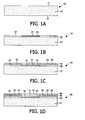
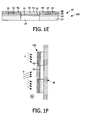
- Figures 1A-1E schematically illustrate subsequent stages in a manufacturing process for manufacturing a first embodiment of a sensor device 100 according to the present invention.
- a silicon wafer 10 is provided. As illustrated in figure 1A , the wafer has a wafer body 13 with two main surfaces 11 and 12. A first main surface. 11will be indicated as top surface and the opposite main surface will be indicated as back surface.
- a first functional layer 20 is manufactured in or on the top surface 11.
- the first functional layer 20 is manufactured such as to comprise a thermal sensor portion 21 with a thermal sensor 23 at a central location in the first functional layer 20, and electronic circuitry 22 arranged around the thermal sensor portion 21.
- a suitable design for the thermal sensor portion 21 will be discussed later.
- the design of the electronic circuitry 22 is basically a free choice of the device designer, depending among other things on the intended use of the sensor, so it is not needed to discuss this design in great detail here. Suffice it to say that the electronic circuitry 22 will be capable of receiving and processing an output signal from the thermal sensor 23.
- the circuitry 22 may include microprocessing capability.
- the processes used for manufacturing the thermal sensor portion 21 and the electronic circuitry 22 may be standard processes that are common in the field of IC manufacturing, so a detailed explanation of such processes is not needed here. It is noted that a suitable technology, especially for making the electronic circuitry 22, is CMOS technology.
- the first functional layer 20 actually comprises a laminate of multiple films arranged is successive steps. These films may include one or more ceramic films, that can act as an etch stop in later etching steps, as will become clearer later.
- a second functional layer 30 is manufactured on the first functional layer 20.
- the second functional layer 30 does not completely cover the first functional layer 20, but it comprises a ring-shaped material portion 32 around an empty space 31.
- This empty space 31 is aligned with the thermal sensor portion 21, and has the same or larger size as the thermal sensor portion 21, so that the ring-shaped material portion 32 leaves the thermal sensor portion 21 completely free: there is no overlap with the thermal sensor 23.
- the second functional layer 30 may be deposited in a ring shape, but it is also possible to deposit the second functional layer 30 over the entire first functional layer 20 and to then partly remove, for instance by etching, the material over the thermal sensor portion 21 so as to leave the ring-shaped material portion 32.
- the second functional layer 30 contains a battery, only schematically indicated at 33.
- the battery 33 has a function of powering the circuitry 22. It is noted that thin film processing used for manufacturing a battery on a semiconductor carrier are known per se, so that a more detailed explanation of such battery design and manufacturing process is not needed here. Several designs for such battery are known, and those known designs can be used here.
- the battery is a solid state battery.
- the second functional layer 30 further contains an antenna, only schematically indicated at 34.
- the antenna has a function of allowing the circuitry 22 to communicate, i.e. to receive command signals and/or to transmit detection signals.
- the circuitry 22 may include a transmitter function, a receiver function, or a transceiver function.
- methods for applying an antenna on a semiconductor carrier are known per se, so that a more detailed explanation of such antenna design and manufacturing process is not needed here.
- such design typically includes a metal line deposited on the semiconductor carrier, possibly spiral-shaped.
- the second functional layer 30 contains an RF harvesting antenna, or that one antenna is used for communication as well as for RF harvesting.
- the manufacturing process for manufacturing the second functional layer 30 is executed at a relatively low temperature, preferably less than 400 °C, so that the components in the first functional layer 20 are not affected by the manufacturing process.
- a suitable example of an all-solid state battery that is capable of being fully manufactured by processing steps below said temperature limit comprises vanadium oxide active electrodes and lithium phosphate-based solid electrolyte.
- a third functional layer 40 containing one or more solar cells 43 is manufactured on the second functional layer 30. Similar as with the second functional layer 30, the third functional layer 40 does not completely cover the second functional layer 30, but it comprises a ring-shaped material portion 42 around an empty space 41. This empty space 41 is aligned with the thermal sensor portion 21, and has the same or larger size as the thermal sensor portion 21, so that the ring-shaped material portion 42 leaves the thermal sensor portion 21 completely free: there is no overlap with the thermal sensor 23.
- the third functional layer 40 may be deposited in a ring shape, but it is also possible to deposit the third functional layer 40 over the entire second functional layer 30 and to then partly remove, for instance by etching, the material over the thermal sensor portion 21 so as to leave the ring-shaped material portion 42.
- the manufacturing process for manufacturing the third functional layer 40 is executed at a temperature lower than the temperature of the manufacturing process for manufacturing the second functional layer 30, preferably less than 300 °C, so that the components in the second functional layer 30 are not affected by the manufacturing process.
- Suitable examples of the manufacturing process are Hot Wire Chemical Vapour Deposition (HWCVD) for producing polychrystalline silicon solar cells, or low temperature Plasma Enhanced Chemical Vapour Deposition (PECVD) for producing amorphous silicon solar cells.
- HWCVD Hot Wire Chemical Vapour Deposition
- PECVD Plasma Enhanced Chemical Vapour Deposition
- a fourth processing stage illustrated in figure 1E , the portion of the wafer body 13 underneath the thermal sensor portion 21 is removed, such as to result in a recess 14 having a depth reaching from the bottom surface 12 side to the thermal sensor portion 21 in the first functional layer 20. Outside this recess 14, part of the wafer body 13 may also be removed in order to reduce the body thickness, as illustrated.
- suitable processes for removing semiconductor material are known per se, so that a more detailed explanation of such process is not needed here.
- suitable examples of such process are reactive ion etching, or sputter etching, or wet chemical etching.
- the etching process stops by an etch stop incorporated in the first functional layer 20, such as a ceramic layer mentioned earlier. Such ceramic layer is not shown separately for sake of simplicity.
- the electrical connections from the solar cell to the battery can easily be provided by suitable design of the topography of the battery and the solar cell, since the solar cell is manufactured directly on top of the battery, as should be clear to a person skilled in the art.
- the electrical connections from the battery to the electronic circuitry 22 can easily be provided by suitable design of the topography of the battery and the electronic circuitry 22, since the battery is manufactured directly on top of the electronic circuitry 22.
- the surface area of the entire device may typically be in the range of 0.1 - 10 cm 2 while the surface area of the thermal sensor portion 21 may typically be in the range of 0.025 - 1 cm 2 .
- the sensor device 100 obtained in this way is very small, and has the advantage of being very flexible due to its small thickness.
- Figure 1F schematically illustrates the use of the sensor device 100.
- the device 100 is attached to a wall W of a room R, oriented such that the bottom surface of the wafer 10 is directed towards the wall W while the third functional layer 40 with the solar cell(s) 43 is directed towards the interior of the room R.
- the solar cell(s) 43 can receive interior light L while the thermal sensor 23 can receive thermal radiation T.
- the wafer 10 acts as carrier for the active layers 20, 30, 40.
- a second embodiment of a sensor device 200 comprises a carrier plate 50 on top of the third functional layer 40 with the solar cell(s) 43.
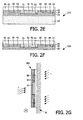
- Figure 2G schematically illustrates the use of this sensor device 200.
- the device 200 is attached to a glass window G of a room R, oriented such that the bottom surface of the wafer 10 is directed towards the interior of the room R while the third functional layer 40 with the solar cell(s) 43 is directed towards the window G.
- the solar cell(s) 43 can receive outside light L while the thermal sensor 23 can receive thermal radiation T from inside the room.
- the carrier plate 50 acts as carrier for the active layers 20, 30, 40.
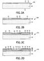
- FIGS 2A-2F schematically illustrate subsequent stages in a manufacturing process for manufacturing this second embodiment of sensor device 200 according to the present invention.
- the wafer is indicated at 210, and differs from the wafer 10 of the first embodiment in that the wafer is a silicon-on-insulator wafer; reference numeral 15 indicates an oxide layer on the top surface 11. This oxide layer 15 is useful for back-etching, but is not essential, so that it is not essential that the wafer 210 is SOI.
- the wafer 10 of the first embodiment may also be SOI.
- the first processing step (illustrated in figure 2B ), second processing step (illustrated in figure 2C ), third processing step (illustrated in figure 2D ) and fourth processing step (illustrated in figure 2F ) are the same as in the first embodiment, so their description will not be repeated.
- Deviating from the first embodiment is a fifth processing step executed between the third and fourth processing steps.
- a glass substrate 50 is attached to the third functional layer 40 (or, vice versa, the wafer 210 is attached to the substrate). Attachment can be performed using a suitable adhesive (not shown) arranged on the third functional layer 40.
- the glass is sufficiently stiff so as not to touch the thermal sensor portion 21, allowing the glass substrate 50 to extend over the thermal sensor portion 21 in order to function as a cover and protection.
- the glass substrate 50 has a thickness of about 200 ⁇ m or more.
- the spaces 31 and 41 above the thermal sensor 23 should remain empty, i.e. any adhesive should not touch the thermal sensor 23. It is possible to apply the adhesive on the glass substrate and then to attach the glass substrate and the wafer to each other. It is also possible to apply the adhesive on the top surface of the wafer (i.e. on the third layer 40), for instance by spinning, and then to attach the glass substrate and the wafer to each other. In both cases, if it is not possible to keep the adhesive away from the thermal sensor 23, it is possible to remove excess adhesive from the thermal sensor by back etching, as should be clear to a person skilled in the art. It is noted that in the fourth step the wafer material is etched away completely, the oxide layer 15 being used as an etch stop. As a result, the mechanical properties of the device are mainly determined by the glass plate.
- the glass plate 50 functions to block all thermal radiation from outside. This function can be improved by applying to the glass plate surface an anti-reflection coating (not shown).
- the carrier plate 50 is made from glass. Instead of glass, it is possible to use another transparent material.
- the carrier plate 50 can be made from polyimide. In order to facilitate handling as far as etching is concerned, it is preferred that a glass plate is attached to the polyimide plate before etching and to remove this glass plate after etching. These steps are not individually illustrated for sake of simplicity.
- all functional layers 20, 30, 40 are arranged at the same side of the wafer substrate.
- the first functional layer with the thermal sensor 23 and the circuitry 22 will be arranged on the silicon substrate 13.
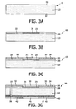
- FIG. 3A-3E schematically illustrate subsequent stages in a manufacturing process for manufacturing this third embodiment of sensor device 300 according to the present invention.
- the first steps as illustrated by figures 3A-3C are identical to the first steps illustrated in figures 1A-1C .
- vias 16 are formed in the substrate 13
- an oxide separation layer 17 is formed on the bottom surface 12 of the wafer
- the third functional layer 40 is manufactured on the said oxide separation layer, as illustrated in figure 3D .
- the vias serve to provide electrical contact between the solar cells 43 and the circuitry 22.
- the step of removing substrate from under the thermal sensor portion 21 as illustrated in figure 3E is identical to the step illustrated in figure 1E , it being noted that the oxide layer is also removed from under the thermal sensor portion 21.
- the third functional layer 40 may be arranged before the second functional layer 30 and even may be arranged before the first functional layer 20.
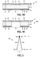
- FIG. 4A-4E schematically illustrate subsequent stages in a manufacturing process for manufacturing this fourth embodiment of sensor device 400 according to the present invention.
- the first steps as illustrated by figures 4A-4B are identical to the first steps illustrated in figures 3A-3B .
- the third functional layer 40 with the solar cells 42 is manufactured on the first functional layer 20, as illustrated in figure 4C .
- Vias 16 are formed in the substrate 13, an oxide separation layer 17 is formed on the bottom surface 12 of the wafer, and then the second functional layer 30 is manufactured on the said oxide separation layer, as illustrated in figure 4D .
- the vias serve to provide electrical contact between the battery 33 and the circuitry 22.
- the step of removing substrate from under the thermal sensor portion 21 as illustrated in figure 4E is identical to the step illustrated in figure 3E .
- FIG. 5 schematically illustrates the basic design of a thermocouple, generally indicated by reference numeral 500.
- the thermocouple 500 comprises two conductive lines 510 and 520 of mutually different material, each having a first end 511, 521 and each having a second end 512, 522.
- the first ends 511, 521 of the lines 510, 520 are connected together.
- T1 first temperature
- T2 second temperature
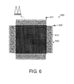
- FIG. 6 schematically illustrates a design of a thermal sensor 600 according to the present invention, suitable for use as the thermal sensor portion 21 mentioned earlier.
- the thermal sensor 600 comprises a central body 610, which may suitable have a square shape, as shown, and which is mounted with as little thermal conduction to its environment as possible.
- a plurality of thermocouples 500 is arranged. Of each thermocouple 500, the joint of first ends 511, 521 is always connected to the central body 610. Further, the free second ends of adjacent thermocouples are connected together, as shown in the partial enlargement, so that all thermocouples are electrically connected in series while thermally being connected in parallel. End terminals of this series arrangement are shown at 601 and 602.
- the central body 610 and the thermocouples 500 are implemented as patterns in silicon.
- the central body 610 is designed to have a relatively large surface area that is heat-absorbing, i.e. absorbing infrared radiation.
- a well-suitable material is black gold.
- the conductive lines 510 and 520 may for instance be made as n-doped and p-doped polysilicon.
- the central body 610 is mounted to receive IR radiation and is implemented in a thin region of silicon, so that it absorbs radiation and rises in temperature without the elevated temperature flowing away easily.
- the conductive lines 510 and 520 may be arranged in a thicker portion of silicon, so that they are better cooled.
- a voltage difference is developed between the end terminals 601, 602, that can directly be used by circuitry arranged in the same chip. It is noted that this sensing voltage does not depend on any supply voltage. It is further noted that the response time of such device is short, in the order of about 10 ms.
- the sensing surface area is relatively large.
- Figures 7 and 8 illustrate embodiments capable of indicating on which part of the sensor the thermal energy is received.
- the sensor device 755 comprises four individual sensors 700, each sensor 700 comprising a central longitudinal body 710 having thermocouples 500 arranged along the opposing longitudinal edges, with end terminals 701 and 702.
- the sensor device 800 comprises a central longitudinal body 810 having thermocouples 500 arranged along the opposing longitudinal edges, with terminals 801 arranged not only at the end but also at intermediate locations, so that sensor signals can be obtained from different portions of the sensor.
- the flexible sensor 755, 800 can be bent so that the different sensor portions can receive thermal radiations from different directions. Thus, it is not only possible to detect the presence of a person, but also to detect a location of such person, and/or to detect a direction of movement of such person.
- the present invention provides a method for manufacturing a sensor device 100; 200; 300; 400 comprising a thermal sensor 23, a battery 33, an antenna 34, an electronic circuitry 22 and a solar cell 43 together integrally in one semiconductor carrier 10.
- the method comprises the steps of:
Landscapes
- Photovoltaic Devices (AREA)
- Photometry And Measurement Of Optical Pulse Characteristics (AREA)
- Investigating Or Analyzing Materials Using Thermal Means (AREA)
- Arrangements For Transmission Of Measured Signals (AREA)
Claims (15)
- Verfahren zur Herstellung einer Sensoreinrichtung (100; 200; 300; 400) mit einem Thermosensor (23), einer Batterie (33), einer Antenne (34), einer elektronischen Schaltung (22) sowie einer Solarzelle (43), die in einem Halbleiterträger (10) einstückig ausgebildet sind, wobei das Verfahren die folgenden Schritte umfasst, wonach:- ein Silicium-Wafer (10) mit einem Wafer-Körper (13) mit zwei gegenüberliegenden, zueinander parallelen Hauptoberflächen (11, 12) vorgesehen wird;- in einer ersten Bearbeitungsstufe eine erste Funktionsschicht (20) in oder auf einer (11) der Hauptoberflächen mit einem Thermosensorteil (21) mit mindestens einem Thermosensor (23) sowie eine Funktionsschicht (20) mit einer, in einer nicht-überlappenden Beziehung mit dem Thermosensorteil (21) angeordneten, elektronischen Schaltung (22) vorgesehen wird;- in einer auf die erste Bearbeitungsstufe folgenden zweiten Bearbeitungsstufe eine zweite Funktionsschicht (30) mit einem eine Batterie (33) und eine Antenne (34) enthaltenden Materialteil (32), der in einer nicht-überlappenden Beziehung mit dem Thermosensorteil (21) angeordnet ist, vorgesehen wird;- in einer auf die erste Bearbeitungsstufe folgenden dritten Bearbeitungsstufe eine dritte Funktionsschicht (40) mit einem eine oder mehrere Solarzellen (43) enthaltenden Materialteil (42), der in einer nicht-überlappenden Beziehung mit dem Thermosensorteil (21) angeordnet ist, vorgesehen wird;- in einer auf die dritte Bearbeitungsstufe folgenden vierten Bearbeitungsstufe der Teil des Wafer-Körpers (13) unterhalb des Thermosensorteils (21) entfernt wird, damit sich eine Aussparung (14) mit einer Tiefe ergibt, die von der Unterseite (12) bis zu dem Thermosensorteil (21) in der ersten Funktionsschicht (20) reicht.
- Verfahren nach Anspruch 1, wobei die elektronische Schaltung (22) und der Thermosensorteil (21) in der gleichen Funktionsschicht (20) vorgesehen werden.
- Verfahren nach Anspruch 2, wobei die elektronische Schaltung (22) und der Thermosensorteil (21) in den gleichen Bearbeitungsstufen vorgesehen werden.
- Verfahren nach Anspruch 1, wobei die zweite Funktionsschicht (30) einen zu dem Thermosensorteil (21) justierten Hohlraum (31) und/oder wobei die dritte Funktionsschicht (40) einen zu dem Thermosensorteil (21) justierten Hohlraum (41) umfasst.
- Verfahren nach Anspruch 1, wobei der Herstellungsprozess zur Herstellung der zweiten Funktionsschicht (30) bei einer relativ niedrigen Temperatur, vorzugsweise weniger als 400°C, ausgeführt wird, so dass die Komponenten in der ersten Funktionsschicht (20) nicht durch diesen Herstellungsprozess geschädigt werden.
- Verfahren nach Anspruch 1, wobei die dritte Bearbeitungsstufe im Anschluss an die zweite Bearbeitungsstufe durchgeführt wird.
- Verfahren nach Anspruch 6, wobei der Herstellungsprozess zur Herstellung der dritten Funktionsschicht (40) bei einer niedrigeren Temperatur als der Temperatur des Herstellungsprozesses zur Herstellung der zweiten Funktionsschicht (30), vorzugsweise bei weniger als 300°C, ausgeführt wird, so dass die Komponenten in der zweiten Funktionsschicht (30) nicht durch diesen Herstellungsprozess geschädigt werden.
- Verfahren nach Anspruch 1, wobei die zweite Funktionsschicht (30) mit Batterie und Antenne auf der ersten Funktionsschicht (20) vorgesehen wird, und wobei die dritte Funktionsschicht (40) mit Solarzelle(n) auf der zweiten Funktionsschicht (30) vorgesehen wird.
- Verfahren nach Anspruch 1, wobei die zweite Funktionsschicht (30) mit Batterie und Antenne auf der ersten Funktionsschicht (20) vorgesehen wird, und wobei die dritte Funktionsschicht (40) mit Solarzelle(n) auf der zweiten (12) der Hauptoberflächen vorgesehen wird.
- Verfahren nach Anspruch 1, wobei die zweite Funktionsschicht (30) mit Batterie und Antenne auf der zweiten (12) der Hauptoberflächen vorgesehen wird, und wobei die dritte Funktionsschicht (40) mit Solarzelle(n) auf der ersten Funktionsschicht (20) vorgesehen wird.
- Verfahren nach Anspruch 1, wobei die dritte Funktionsschicht (40) mit Solarzelle(n) als äußerste Schicht vorgesehen wird, und wobei eine Trägerplatte (50) auf der Oberseite dieser dritten Funktionsschicht vorgesehen wird, wobei die Trägerplatte vorzugsweise aus Glas oder Polyimid gefertigt wird.
- Sensoreinrichtung mit einem Thermosensor (23), einer Batterie (33), einer Antenne (34), einer elektronischen Schaltung (22), einer Solarzelle (43) sowie einem in einer nicht-überlappenden Beziehung mit der elektronischen Schaltung (22) in einer Funktionsschicht der Sensoreinrichtung angeordneten Thermosensorteil (21), wobei die Sensoreinrichtung in einem Verfahren nach einem der Ansprüche 1 bis 11 in einem Halbleiterkörper (13) einstückig hergestellt wird.
- Sensoreinrichtung nach Anspruch 12, wobei der Thermosensor (23) einen dünnen, zentralen Körper (610) sowie mehrere entlang den Rändern des zentralen Körpers (610) angeordnete Thermoelemente (500) umfasst;
wobei der zentrale Körper (610) als wärmeabsorbierend ausgeführt ist; wobei sämtliche Thermoelemente elektrisch in Reihe und dabei thermisch parallel geschaltet sind;
und wobei der zentrale Körper (610) und die Thermoelemente (500) als Strukturen in Silicium implementiert sind. - Sensoreinrichtung nach Anspruch 12, wobei der Thermosensor (23) vier einzelne Sensorteile (700) umfasst, wobei jeder Sensorteil (700) einen dünnen, zentralen Längskörper (710) und mehrere entlang den sich gegenüberliegenden Längsrändern des zentralen Körpers (710) angeordnete Thermoelemente (500) umfasst.
- Sensoreinrichtung nach Anspruch 12, wobei der Thermosensor (23) einen dünnen, zentralen Längskörper (810) und mehrere entlang den sich gegenüberliegenden Längsrändern des zentralen Körpers (810) angeordnete Thermoelemente (500) mit mit den Thermoendelementen in Kontakt kommenden Anschlüssen (801) und ebenfalls mit mit Thermozwischenelementen in Kontakt kommenden Anschlüssen (801) umfasst, so dass Sensorsignale von verschiedenen Teilen des Sensors empfangen werden können.
Priority Applications (1)
| Application Number | Priority Date | Filing Date | Title |
|---|---|---|---|
| EP10719627A EP2436237B1 (de) | 2009-05-27 | 2010-05-07 | Belegungssensor |
Applications Claiming Priority (3)
| Application Number | Priority Date | Filing Date | Title |
|---|---|---|---|
| EP09161189 | 2009-05-27 | ||
| PCT/IB2010/052020 WO2010136919A1 (en) | 2009-05-27 | 2010-05-07 | Occupancy sensor |
| EP10719627A EP2436237B1 (de) | 2009-05-27 | 2010-05-07 | Belegungssensor |
Publications (2)
| Publication Number | Publication Date |
|---|---|
| EP2436237A1 EP2436237A1 (de) | 2012-04-04 |
| EP2436237B1 true EP2436237B1 (de) | 2012-12-26 |
Family
ID=42946153
Family Applications (1)
| Application Number | Title | Priority Date | Filing Date |
|---|---|---|---|
| EP10719627A Not-in-force EP2436237B1 (de) | 2009-05-27 | 2010-05-07 | Belegungssensor |
Country Status (8)
| Country | Link |
|---|---|
| US (1) | US8357550B2 (de) |
| EP (1) | EP2436237B1 (de) |
| JP (1) | JP5398908B2 (de) |
| KR (1) | KR20120020186A (de) |
| CN (1) | CN102450106B (de) |
| CA (1) | CA2763240A1 (de) |
| RU (1) | RU2011153187A (de) |
| WO (1) | WO2010136919A1 (de) |
Families Citing this family (16)
| Publication number | Priority date | Publication date | Assignee | Title |
|---|---|---|---|---|
| DE102010062559A1 (de) * | 2010-12-07 | 2012-06-14 | Robert Bosch Gmbh | Mikroelektromechanisches Sensormodul sowie entsprechendes Herstellungsverfahren |
| US8569861B2 (en) * | 2010-12-22 | 2013-10-29 | Analog Devices, Inc. | Vertically integrated systems |
| MX336866B (es) * | 2011-12-21 | 2016-02-04 | Dow Global Technologies Llc | Metodo mejorado para producir dos o mas celdas fotovaltaicas interconectadas basadas en pelicula delgada. |
| US10557881B2 (en) | 2015-03-27 | 2020-02-11 | Analog Devices Global | Electrical overstress reporting |
| US9871373B2 (en) | 2015-03-27 | 2018-01-16 | Analog Devices Global | Electrical overstress recording and/or harvesting |
| KR20170089340A (ko) * | 2016-01-26 | 2017-08-03 | 엘지전자 주식회사 | 플렉서블 센서 모듈 및 이의 제조 방법 |
| US10338132B2 (en) | 2016-04-19 | 2019-07-02 | Analog Devices Global | Wear-out monitor device |
| US10365322B2 (en) | 2016-04-19 | 2019-07-30 | Analog Devices Global | Wear-out monitor device |
| DE102017011673A1 (de) * | 2016-12-21 | 2018-06-21 | Marquardt Gmbh | Sensorsystem mit einer Solarzelle |
| EP3625554B1 (de) | 2017-05-15 | 2026-06-24 | Analog Devices International Unlimited Company | Integrierter ionen-messvorrichtung und verfahren |
| US11024525B2 (en) | 2017-06-12 | 2021-06-01 | Analog Devices International Unlimited Company | Diffusion temperature shock monitor |
| US10730743B2 (en) | 2017-11-06 | 2020-08-04 | Analog Devices Global Unlimited Company | Gas sensor packages |
| US11587839B2 (en) | 2019-06-27 | 2023-02-21 | Analog Devices, Inc. | Device with chemical reaction chamber |
| US10777611B1 (en) * | 2019-09-27 | 2020-09-15 | Sony Semiconductor Solutions Corporation | Image sensor |
| US12474290B2 (en) | 2019-11-20 | 2025-11-18 | Analog Devices International Unlimited Company | Electrochemical device |
| JP2021118551A (ja) * | 2020-01-22 | 2021-08-10 | ソニーセミコンダクタソリューションズ株式会社 | 撮像装置、センサ装置及び電子機器 |
Family Cites Families (18)
| Publication number | Priority date | Publication date | Assignee | Title |
|---|---|---|---|---|
| US10103A (en) * | 1853-10-11 | Detachable lining for the fire-boxes of steam-boilers | ||
| JPH08304174A (ja) * | 1995-04-28 | 1996-11-22 | Fujitsu Ltd | サーモパイル赤外線センサおよびセンサアレイ |
| JPH10242443A (ja) * | 1997-02-27 | 1998-09-11 | Toshiba Corp | 機能集積半導体装置 |
| DE10222499A1 (de) * | 2002-05-22 | 2003-12-11 | Bosch Gmbh Robert | Verfahren zur Herstellung eines Bauteils, insbesondere eines thermischen Sensors, sowie thermischer Sensor |
| JP2004093535A (ja) * | 2002-09-04 | 2004-03-25 | Mitsubishi Electric Corp | 熱型赤外線固体撮像装置およびその製造方法 |
| US7868358B2 (en) * | 2003-06-06 | 2011-01-11 | Northrop Grumman Systems Corporation | Coiled circuit device with active circuitry and methods for making the same |
| JP2005106802A (ja) * | 2003-07-10 | 2005-04-21 | Canon Inc | 環境センサー、環境測定装置及び環境測定システム |
| EP1523043B1 (de) * | 2003-10-06 | 2011-12-28 | Semiconductor Energy Laboratory Co., Ltd. | Optischer Sensor und dessen Herstellungsverfahren |
| GB0408073D0 (en) * | 2004-04-08 | 2004-05-12 | Council Cent Lab Res Councils | Optical sensor |
| JPWO2006132155A1 (ja) | 2005-06-06 | 2009-01-08 | 松下電器産業株式会社 | 電子デバイス及びその製造方法 |
| US8173519B2 (en) * | 2006-03-03 | 2012-05-08 | Semiconductor Energy Laboratory Co., Ltd. | Method for manufacturing semiconductor device |
| JP2007280368A (ja) * | 2006-03-15 | 2007-10-25 | Semiconductor Energy Lab Co Ltd | 半導体装置及び当該半導体装置を具備するidラベル、idタグ、idカード |
| WO2007130471A2 (en) * | 2006-05-01 | 2007-11-15 | The Charles Stark Draper Laboratory, Inc. | Systems and methods for high density multi-component modules |
| EP2012658A2 (de) * | 2006-05-04 | 2009-01-14 | CardioMems, Inc. | Implantierbarer drahtloser sensor zur in-vivo-druckmessung und zur kontinuierlichen ergebnisbestimmung |
| US8459445B2 (en) * | 2006-07-21 | 2013-06-11 | Menicon, Co., Ltd. | Colored contact lens primary packaging |
| JP2008066402A (ja) * | 2006-09-05 | 2008-03-21 | Fujifilm Corp | 撮像素子および撮像装置 |
| US20080109309A1 (en) | 2006-10-31 | 2008-05-08 | Steven Landau | Powered Print Advertisements, Product Packaging, and Trading Cards |
| WO2009150562A1 (en) | 2008-06-11 | 2009-12-17 | Koninklijke Philips Electronics N.V. | Wireless sensor device and illumination system comprising such a device |
-
2010
- 2010-05-07 EP EP10719627A patent/EP2436237B1/de not_active Not-in-force
- 2010-05-07 CN CN201080023392.3A patent/CN102450106B/zh not_active Expired - Fee Related
- 2010-05-07 CA CA2763240A patent/CA2763240A1/en not_active Abandoned
- 2010-05-07 US US13/322,296 patent/US8357550B2/en not_active Expired - Fee Related
- 2010-05-07 RU RU2011153187/07A patent/RU2011153187A/ru not_active Application Discontinuation
- 2010-05-07 WO PCT/IB2010/052020 patent/WO2010136919A1/en not_active Ceased
- 2010-05-07 KR KR1020117031004A patent/KR20120020186A/ko not_active Withdrawn
- 2010-05-07 JP JP2012512478A patent/JP5398908B2/ja not_active Expired - Fee Related
Also Published As
| Publication number | Publication date |
|---|---|
| CN102450106A (zh) | 2012-05-09 |
| JP2012528322A (ja) | 2012-11-12 |
| US8357550B2 (en) | 2013-01-22 |
| US20120077291A1 (en) | 2012-03-29 |
| JP5398908B2 (ja) | 2014-01-29 |
| KR20120020186A (ko) | 2012-03-07 |
| CN102450106B (zh) | 2014-07-16 |
| CA2763240A1 (en) | 2010-12-02 |
| EP2436237A1 (de) | 2012-04-04 |
| WO2010136919A1 (en) | 2010-12-02 |
| RU2011153187A (ru) | 2013-07-10 |
Similar Documents
| Publication | Publication Date | Title |
|---|---|---|
| US8357550B2 (en) | Occupancy sensor | |
| RU2529659C2 (ru) | Способ изготовления мультипереходных и многоэлектродных фотогальванических элементов | |
| CN103843462A (zh) | 发光设备 | |
| TW200913291A (en) | Photovoltaic modules with integrated devices | |
| WO2004038810A3 (en) | Circuit substrate and method | |
| FR2811778B1 (fr) | Dispositif electrochimique du type electrochrome ou dispositif photovoltaique et ses moyens de connexion electrique | |
| WO2010035269A2 (en) | Integrated solar powered device | |
| US9379265B2 (en) | Integrated circuit combination of a target integrated circuit, photovoltaic cells and light sensitive diodes connected to enable a self-sufficient light detector device | |
| CN102484436A (zh) | 发电装置及具备该发电装置的发电系统 | |
| US20090288700A1 (en) | Integrated device | |
| WO2014057543A1 (ja) | 熱電変換装置および電子装置 | |
| WO2005004242A3 (en) | Solar cell with an electrically insulating layer under the busbar | |
| WO2011075967A1 (zh) | 搪瓷太阳能建筑墙板 | |
| WO2014132197A3 (en) | Integrated photovoltaic and thermal module (pvt) | |
| US10530018B2 (en) | Panel, a method for fabricating a panel and a method | |
| CN103500768A (zh) | 一种柔性太阳能组件及其制作方法 | |
| WO2025175950A1 (zh) | 曲面光伏件 | |
| CN102508577A (zh) | 太阳能触感式控制面板 | |
| KR101294020B1 (ko) | 태양전지를 이용한 조명 장치 | |
| CN117213635A (zh) | 一种基于人体红外辐射探测的非接触式人机交互系统 | |
| US20130327163A1 (en) | Microelectromechanical sensor module and corresponding production method | |
| US10170655B2 (en) | Energy harvesting device with prefabricated thin film energy absorption sheets and roll-to-sheet and roll-to-roll fabrication thereof | |
| CN202331407U (zh) | 太阳能触感式控制面板 | |
| EP2380212B1 (de) | Photovoltaiksystem für eine elektronische Vorrichtung | |
| JP2012009690A (ja) | 光センサー、それを用いた火災報知機及び光センサーの製造方法 |
Legal Events
| Date | Code | Title | Description |
|---|---|---|---|
| PUAI | Public reference made under article 153(3) epc to a published international application that has entered the european phase |
Free format text: ORIGINAL CODE: 0009012 |
|
| 17P | Request for examination filed |
Effective date: 20111227 |
|
| AK | Designated contracting states |
Kind code of ref document: A1 Designated state(s): AL AT BE BG CH CY CZ DE DK EE ES FI FR GB GR HR HU IE IS IT LI LT LU LV MC MK MT NL NO PL PT RO SE SI SK SM TR |
|
| REG | Reference to a national code |
Ref country code: DE Ref legal event code: R079 Ref document number: 602010004340 Country of ref document: DE Free format text: PREVIOUS MAIN CLASS: H05B0037020000 Ipc: H01L0031101000 |
|
| GRAP | Despatch of communication of intention to grant a patent |
Free format text: ORIGINAL CODE: EPIDOSNIGR1 |
|
| RIC1 | Information provided on ipc code assigned before grant |
Ipc: H05B 37/02 20060101ALI20120629BHEP Ipc: H01L 31/18 20060101ALI20120629BHEP Ipc: H01L 27/14 20060101ALI20120629BHEP Ipc: H01L 31/101 20060101AFI20120629BHEP |
|
| DAX | Request for extension of the european patent (deleted) | ||
| GRAS | Grant fee paid |
Free format text: ORIGINAL CODE: EPIDOSNIGR3 |
|
| GRAA | (expected) grant |
Free format text: ORIGINAL CODE: 0009210 |
|
| AK | Designated contracting states |
Kind code of ref document: B1 Designated state(s): AL AT BE BG CH CY CZ DE DK EE ES FI FR GB GR HR HU IE IS IT LI LT LU LV MC MK MT NL NO PL PT RO SE SI SK SM TR |
|
| REG | Reference to a national code |
Ref country code: GB Ref legal event code: FG4D |
|
| REG | Reference to a national code |
Ref country code: CH Ref legal event code: EP |
|
| REG | Reference to a national code |
Ref country code: AT Ref legal event code: REF Ref document number: 590864 Country of ref document: AT Kind code of ref document: T Effective date: 20130115 |
|
| REG | Reference to a national code |
Ref country code: DE Ref legal event code: R096 Ref document number: 602010004340 Country of ref document: DE Effective date: 20130314 |
|
| PG25 | Lapsed in a contracting state [announced via postgrant information from national office to epo] |
Ref country code: FI Free format text: LAPSE BECAUSE OF FAILURE TO SUBMIT A TRANSLATION OF THE DESCRIPTION OR TO PAY THE FEE WITHIN THE PRESCRIBED TIME-LIMIT Effective date: 20121226 Ref country code: NO Free format text: LAPSE BECAUSE OF FAILURE TO SUBMIT A TRANSLATION OF THE DESCRIPTION OR TO PAY THE FEE WITHIN THE PRESCRIBED TIME-LIMIT Effective date: 20130326 Ref country code: HR Free format text: LAPSE BECAUSE OF FAILURE TO SUBMIT A TRANSLATION OF THE DESCRIPTION OR TO PAY THE FEE WITHIN THE PRESCRIBED TIME-LIMIT Effective date: 20121226 Ref country code: LT Free format text: LAPSE BECAUSE OF FAILURE TO SUBMIT A TRANSLATION OF THE DESCRIPTION OR TO PAY THE FEE WITHIN THE PRESCRIBED TIME-LIMIT Effective date: 20121226 Ref country code: SE Free format text: LAPSE BECAUSE OF FAILURE TO SUBMIT A TRANSLATION OF THE DESCRIPTION OR TO PAY THE FEE WITHIN THE PRESCRIBED TIME-LIMIT Effective date: 20121226 |
|
| REG | Reference to a national code |
Ref country code: AT Ref legal event code: MK05 Ref document number: 590864 Country of ref document: AT Kind code of ref document: T Effective date: 20121226 |
|
| REG | Reference to a national code |
Ref country code: LT Ref legal event code: MG4D |
|
| REG | Reference to a national code |
Ref country code: NL Ref legal event code: VDEP Effective date: 20121226 |
|
| PG25 | Lapsed in a contracting state [announced via postgrant information from national office to epo] |
Ref country code: GR Free format text: LAPSE BECAUSE OF FAILURE TO SUBMIT A TRANSLATION OF THE DESCRIPTION OR TO PAY THE FEE WITHIN THE PRESCRIBED TIME-LIMIT Effective date: 20130327 Ref country code: SI Free format text: LAPSE BECAUSE OF FAILURE TO SUBMIT A TRANSLATION OF THE DESCRIPTION OR TO PAY THE FEE WITHIN THE PRESCRIBED TIME-LIMIT Effective date: 20121226 Ref country code: LV Free format text: LAPSE BECAUSE OF FAILURE TO SUBMIT A TRANSLATION OF THE DESCRIPTION OR TO PAY THE FEE WITHIN THE PRESCRIBED TIME-LIMIT Effective date: 20121226 |
|
| PG25 | Lapsed in a contracting state [announced via postgrant information from national office to epo] |
Ref country code: IS Free format text: LAPSE BECAUSE OF FAILURE TO SUBMIT A TRANSLATION OF THE DESCRIPTION OR TO PAY THE FEE WITHIN THE PRESCRIBED TIME-LIMIT Effective date: 20130426 Ref country code: BE Free format text: LAPSE BECAUSE OF FAILURE TO SUBMIT A TRANSLATION OF THE DESCRIPTION OR TO PAY THE FEE WITHIN THE PRESCRIBED TIME-LIMIT Effective date: 20121226 Ref country code: BG Free format text: LAPSE BECAUSE OF FAILURE TO SUBMIT A TRANSLATION OF THE DESCRIPTION OR TO PAY THE FEE WITHIN THE PRESCRIBED TIME-LIMIT Effective date: 20130326 Ref country code: EE Free format text: LAPSE BECAUSE OF FAILURE TO SUBMIT A TRANSLATION OF THE DESCRIPTION OR TO PAY THE FEE WITHIN THE PRESCRIBED TIME-LIMIT Effective date: 20121226 Ref country code: SK Free format text: LAPSE BECAUSE OF FAILURE TO SUBMIT A TRANSLATION OF THE DESCRIPTION OR TO PAY THE FEE WITHIN THE PRESCRIBED TIME-LIMIT Effective date: 20121226 Ref country code: ES Free format text: LAPSE BECAUSE OF FAILURE TO SUBMIT A TRANSLATION OF THE DESCRIPTION OR TO PAY THE FEE WITHIN THE PRESCRIBED TIME-LIMIT Effective date: 20130406 Ref country code: AT Free format text: LAPSE BECAUSE OF FAILURE TO SUBMIT A TRANSLATION OF THE DESCRIPTION OR TO PAY THE FEE WITHIN THE PRESCRIBED TIME-LIMIT Effective date: 20121226 Ref country code: CZ Free format text: LAPSE BECAUSE OF FAILURE TO SUBMIT A TRANSLATION OF THE DESCRIPTION OR TO PAY THE FEE WITHIN THE PRESCRIBED TIME-LIMIT Effective date: 20121226 |
|
| PG25 | Lapsed in a contracting state [announced via postgrant information from national office to epo] |
Ref country code: NL Free format text: LAPSE BECAUSE OF FAILURE TO SUBMIT A TRANSLATION OF THE DESCRIPTION OR TO PAY THE FEE WITHIN THE PRESCRIBED TIME-LIMIT Effective date: 20121226 Ref country code: PL Free format text: LAPSE BECAUSE OF FAILURE TO SUBMIT A TRANSLATION OF THE DESCRIPTION OR TO PAY THE FEE WITHIN THE PRESCRIBED TIME-LIMIT Effective date: 20121226 Ref country code: PT Free format text: LAPSE BECAUSE OF FAILURE TO SUBMIT A TRANSLATION OF THE DESCRIPTION OR TO PAY THE FEE WITHIN THE PRESCRIBED TIME-LIMIT Effective date: 20130426 Ref country code: RO Free format text: LAPSE BECAUSE OF FAILURE TO SUBMIT A TRANSLATION OF THE DESCRIPTION OR TO PAY THE FEE WITHIN THE PRESCRIBED TIME-LIMIT Effective date: 20121226 |
|
| REG | Reference to a national code |
Ref country code: CH Ref legal event code: PFA Owner name: KONINKLIJKE PHILIPS N.V., NL Free format text: FORMER OWNER: KONINKLIJKE PHILIPS ELECTRONICS N.V., NL |
|
| RAP2 | Party data changed (patent owner data changed or rights of a patent transferred) |
Owner name: KONINKLIJKE PHILIPS N.V. |
|
| PG25 | Lapsed in a contracting state [announced via postgrant information from national office to epo] |
Ref country code: DK Free format text: LAPSE BECAUSE OF FAILURE TO SUBMIT A TRANSLATION OF THE DESCRIPTION OR TO PAY THE FEE WITHIN THE PRESCRIBED TIME-LIMIT Effective date: 20121226 |
|
| PLBE | No opposition filed within time limit |
Free format text: ORIGINAL CODE: 0009261 |
|
| STAA | Information on the status of an ep patent application or granted ep patent |
Free format text: STATUS: NO OPPOSITION FILED WITHIN TIME LIMIT |
|
| PG25 | Lapsed in a contracting state [announced via postgrant information from national office to epo] |
Ref country code: CY Free format text: LAPSE BECAUSE OF FAILURE TO SUBMIT A TRANSLATION OF THE DESCRIPTION OR TO PAY THE FEE WITHIN THE PRESCRIBED TIME-LIMIT Effective date: 20121226 |
|
| 26N | No opposition filed |
Effective date: 20130927 |
|
| PG25 | Lapsed in a contracting state [announced via postgrant information from national office to epo] |
Ref country code: MC Free format text: LAPSE BECAUSE OF FAILURE TO SUBMIT A TRANSLATION OF THE DESCRIPTION OR TO PAY THE FEE WITHIN THE PRESCRIBED TIME-LIMIT Effective date: 20121226 Ref country code: IT Free format text: LAPSE BECAUSE OF FAILURE TO SUBMIT A TRANSLATION OF THE DESCRIPTION OR TO PAY THE FEE WITHIN THE PRESCRIBED TIME-LIMIT Effective date: 20121226 |
|
| REG | Reference to a national code |
Ref country code: DE Ref legal event code: R097 Ref document number: 602010004340 Country of ref document: DE Effective date: 20130927 |
|
| REG | Reference to a national code |
Ref country code: IE Ref legal event code: MM4A |
|
| PG25 | Lapsed in a contracting state [announced via postgrant information from national office to epo] |
Ref country code: IE Free format text: LAPSE BECAUSE OF NON-PAYMENT OF DUE FEES Effective date: 20130507 |
|
| REG | Reference to a national code |
Ref country code: DE Ref legal event code: R081 Ref document number: 602010004340 Country of ref document: DE Owner name: KONINKLIJKE PHILIPS N.V., NL Free format text: FORMER OWNER: KONINKLIJKE PHILIPS ELECTRONICS N.V., EINDHOVEN, NL Effective date: 20140328 |
|
| PGFP | Annual fee paid to national office [announced via postgrant information from national office to epo] |
Ref country code: GB Payment date: 20140530 Year of fee payment: 5 |
|
| PGFP | Annual fee paid to national office [announced via postgrant information from national office to epo] |
Ref country code: DE Payment date: 20140731 Year of fee payment: 5 |
|
| PGFP | Annual fee paid to national office [announced via postgrant information from national office to epo] |
Ref country code: FR Payment date: 20140528 Year of fee payment: 5 |
|
| REG | Reference to a national code |
Ref country code: CH Ref legal event code: PL |
|
| PG25 | Lapsed in a contracting state [announced via postgrant information from national office to epo] |
Ref country code: LI Free format text: LAPSE BECAUSE OF NON-PAYMENT OF DUE FEES Effective date: 20140531 Ref country code: CH Free format text: LAPSE BECAUSE OF NON-PAYMENT OF DUE FEES Effective date: 20140531 |
|
| PG25 | Lapsed in a contracting state [announced via postgrant information from national office to epo] |
Ref country code: MT Free format text: LAPSE BECAUSE OF FAILURE TO SUBMIT A TRANSLATION OF THE DESCRIPTION OR TO PAY THE FEE WITHIN THE PRESCRIBED TIME-LIMIT Effective date: 20121226 |
|
| PG25 | Lapsed in a contracting state [announced via postgrant information from national office to epo] |
Ref country code: SM Free format text: LAPSE BECAUSE OF FAILURE TO SUBMIT A TRANSLATION OF THE DESCRIPTION OR TO PAY THE FEE WITHIN THE PRESCRIBED TIME-LIMIT Effective date: 20121226 |
|
| PG25 | Lapsed in a contracting state [announced via postgrant information from national office to epo] |
Ref country code: TR Free format text: LAPSE BECAUSE OF FAILURE TO SUBMIT A TRANSLATION OF THE DESCRIPTION OR TO PAY THE FEE WITHIN THE PRESCRIBED TIME-LIMIT Effective date: 20121226 |
|
| PG25 | Lapsed in a contracting state [announced via postgrant information from national office to epo] |
Ref country code: LU Free format text: LAPSE BECAUSE OF NON-PAYMENT OF DUE FEES Effective date: 20130507 Ref country code: MK Free format text: LAPSE BECAUSE OF FAILURE TO SUBMIT A TRANSLATION OF THE DESCRIPTION OR TO PAY THE FEE WITHIN THE PRESCRIBED TIME-LIMIT Effective date: 20121226 Ref country code: HU Free format text: LAPSE BECAUSE OF FAILURE TO SUBMIT A TRANSLATION OF THE DESCRIPTION OR TO PAY THE FEE WITHIN THE PRESCRIBED TIME-LIMIT; INVALID AB INITIO Effective date: 20100507 |
|
| REG | Reference to a national code |
Ref country code: DE Ref legal event code: R119 Ref document number: 602010004340 Country of ref document: DE |
|
| GBPC | Gb: european patent ceased through non-payment of renewal fee |
Effective date: 20150507 |
|
| REG | Reference to a national code |
Ref country code: FR Ref legal event code: ST Effective date: 20160129 |
|
| PG25 | Lapsed in a contracting state [announced via postgrant information from national office to epo] |
Ref country code: DE Free format text: LAPSE BECAUSE OF NON-PAYMENT OF DUE FEES Effective date: 20151201 Ref country code: GB Free format text: LAPSE BECAUSE OF NON-PAYMENT OF DUE FEES Effective date: 20150507 |
|
| PG25 | Lapsed in a contracting state [announced via postgrant information from national office to epo] |
Ref country code: FR Free format text: LAPSE BECAUSE OF NON-PAYMENT OF DUE FEES Effective date: 20150601 |
|
| PG25 | Lapsed in a contracting state [announced via postgrant information from national office to epo] |
Ref country code: AL Free format text: LAPSE BECAUSE OF FAILURE TO SUBMIT A TRANSLATION OF THE DESCRIPTION OR TO PAY THE FEE WITHIN THE PRESCRIBED TIME-LIMIT Effective date: 20121226 |