EP2431802A1 - Flüssigkristallanzeigevorrichtung und Herstellungsverfahren dafür - Google Patents
Flüssigkristallanzeigevorrichtung und Herstellungsverfahren dafür Download PDFInfo
- Publication number
- EP2431802A1 EP2431802A1 EP11007618A EP11007618A EP2431802A1 EP 2431802 A1 EP2431802 A1 EP 2431802A1 EP 11007618 A EP11007618 A EP 11007618A EP 11007618 A EP11007618 A EP 11007618A EP 2431802 A1 EP2431802 A1 EP 2431802A1
- Authority
- EP
- European Patent Office
- Prior art keywords
- contact
- metal
- gate metal
- common electrode
- gate
- Prior art date
- Legal status (The legal status is an assumption and is not a legal conclusion. Google has not performed a legal analysis and makes no representation as to the accuracy of the status listed.)
- Granted
Links
Images


Classifications
-
- G—PHYSICS
- G02—OPTICS
- G02F—OPTICAL DEVICES OR ARRANGEMENTS FOR THE CONTROL OF LIGHT BY MODIFICATION OF THE OPTICAL PROPERTIES OF THE MEDIA OF THE ELEMENTS INVOLVED THEREIN; NON-LINEAR OPTICS; FREQUENCY-CHANGING OF LIGHT; OPTICAL LOGIC ELEMENTS; OPTICAL ANALOGUE/DIGITAL CONVERTERS
- G02F1/00—Devices or arrangements for the control of the intensity, colour, phase, polarisation or direction of light arriving from an independent light source, e.g. switching, gating or modulating; Non-linear optics
- G02F1/01—Devices or arrangements for the control of the intensity, colour, phase, polarisation or direction of light arriving from an independent light source, e.g. switching, gating or modulating; Non-linear optics for the control of the intensity, phase, polarisation or colour
- G02F1/13—Devices or arrangements for the control of the intensity, colour, phase, polarisation or direction of light arriving from an independent light source, e.g. switching, gating or modulating; Non-linear optics for the control of the intensity, phase, polarisation or colour based on liquid crystals, e.g. single liquid crystal display cells
- G02F1/133—Constructional arrangements; Operation of liquid crystal cells; Circuit arrangements
- G02F1/136—Liquid crystal cells structurally associated with a semi-conducting layer or substrate, e.g. cells forming part of an integrated circuit
- G02F1/1362—Active matrix addressed cells
- G02F1/136227—Through-hole connection of the pixel electrode to the active element through an insulation layer
-
- G—PHYSICS
- G06—COMPUTING OR CALCULATING; COUNTING
- G06F—ELECTRIC DIGITAL DATA PROCESSING
- G06F3/00—Input arrangements for transferring data to be processed into a form capable of being handled by the computer; Output arrangements for transferring data from processing unit to output unit, e.g. interface arrangements
- G06F3/01—Input arrangements or combined input and output arrangements for interaction between user and computer
- G06F3/03—Arrangements for converting the position or the displacement of a member into a coded form
- G06F3/041—Digitisers, e.g. for touch screens or touch pads, characterised by the transducing means
- G06F3/0412—Digitisers structurally integrated in a display
-
- G—PHYSICS
- G06—COMPUTING OR CALCULATING; COUNTING
- G06F—ELECTRIC DIGITAL DATA PROCESSING
- G06F3/00—Input arrangements for transferring data to be processed into a form capable of being handled by the computer; Output arrangements for transferring data from processing unit to output unit, e.g. interface arrangements
- G06F3/01—Input arrangements or combined input and output arrangements for interaction between user and computer
- G06F3/03—Arrangements for converting the position or the displacement of a member into a coded form
- G06F3/041—Digitisers, e.g. for touch screens or touch pads, characterised by the transducing means
- G06F3/044—Digitisers, e.g. for touch screens or touch pads, characterised by the transducing means by capacitive means
- G06F3/0443—Digitisers, e.g. for touch screens or touch pads, characterised by the transducing means by capacitive means using a single layer of sensing electrodes
-
- G—PHYSICS
- G02—OPTICS
- G02F—OPTICAL DEVICES OR ARRANGEMENTS FOR THE CONTROL OF LIGHT BY MODIFICATION OF THE OPTICAL PROPERTIES OF THE MEDIA OF THE ELEMENTS INVOLVED THEREIN; NON-LINEAR OPTICS; FREQUENCY-CHANGING OF LIGHT; OPTICAL LOGIC ELEMENTS; OPTICAL ANALOGUE/DIGITAL CONVERTERS
- G02F1/00—Devices or arrangements for the control of the intensity, colour, phase, polarisation or direction of light arriving from an independent light source, e.g. switching, gating or modulating; Non-linear optics
- G02F1/01—Devices or arrangements for the control of the intensity, colour, phase, polarisation or direction of light arriving from an independent light source, e.g. switching, gating or modulating; Non-linear optics for the control of the intensity, phase, polarisation or colour
- G02F1/13—Devices or arrangements for the control of the intensity, colour, phase, polarisation or direction of light arriving from an independent light source, e.g. switching, gating or modulating; Non-linear optics for the control of the intensity, phase, polarisation or colour based on liquid crystals, e.g. single liquid crystal display cells
- G02F1/133—Constructional arrangements; Operation of liquid crystal cells; Circuit arrangements
- G02F1/1333—Constructional arrangements; Manufacturing methods
- G02F1/13338—Input devices, e.g. touch panels
-
- G—PHYSICS
- G02—OPTICS
- G02F—OPTICAL DEVICES OR ARRANGEMENTS FOR THE CONTROL OF LIGHT BY MODIFICATION OF THE OPTICAL PROPERTIES OF THE MEDIA OF THE ELEMENTS INVOLVED THEREIN; NON-LINEAR OPTICS; FREQUENCY-CHANGING OF LIGHT; OPTICAL LOGIC ELEMENTS; OPTICAL ANALOGUE/DIGITAL CONVERTERS
- G02F1/00—Devices or arrangements for the control of the intensity, colour, phase, polarisation or direction of light arriving from an independent light source, e.g. switching, gating or modulating; Non-linear optics
- G02F1/01—Devices or arrangements for the control of the intensity, colour, phase, polarisation or direction of light arriving from an independent light source, e.g. switching, gating or modulating; Non-linear optics for the control of the intensity, phase, polarisation or colour
- G02F1/13—Devices or arrangements for the control of the intensity, colour, phase, polarisation or direction of light arriving from an independent light source, e.g. switching, gating or modulating; Non-linear optics for the control of the intensity, phase, polarisation or colour based on liquid crystals, e.g. single liquid crystal display cells
- G02F1/133—Constructional arrangements; Operation of liquid crystal cells; Circuit arrangements
- G02F1/136—Liquid crystal cells structurally associated with a semi-conducting layer or substrate, e.g. cells forming part of an integrated circuit
- G02F1/1362—Active matrix addressed cells
- G02F1/136286—Wiring, e.g. gate line, drain line
- G02F1/13629—Multilayer wirings
-
- G—PHYSICS
- G02—OPTICS
- G02F—OPTICAL DEVICES OR ARRANGEMENTS FOR THE CONTROL OF LIGHT BY MODIFICATION OF THE OPTICAL PROPERTIES OF THE MEDIA OF THE ELEMENTS INVOLVED THEREIN; NON-LINEAR OPTICS; FREQUENCY-CHANGING OF LIGHT; OPTICAL LOGIC ELEMENTS; OPTICAL ANALOGUE/DIGITAL CONVERTERS
- G02F1/00—Devices or arrangements for the control of the intensity, colour, phase, polarisation or direction of light arriving from an independent light source, e.g. switching, gating or modulating; Non-linear optics
- G02F1/01—Devices or arrangements for the control of the intensity, colour, phase, polarisation or direction of light arriving from an independent light source, e.g. switching, gating or modulating; Non-linear optics for the control of the intensity, phase, polarisation or colour
- G02F1/13—Devices or arrangements for the control of the intensity, colour, phase, polarisation or direction of light arriving from an independent light source, e.g. switching, gating or modulating; Non-linear optics for the control of the intensity, phase, polarisation or colour based on liquid crystals, e.g. single liquid crystal display cells
- G02F1/133—Constructional arrangements; Operation of liquid crystal cells; Circuit arrangements
- G02F1/136—Liquid crystal cells structurally associated with a semi-conducting layer or substrate, e.g. cells forming part of an integrated circuit
- G02F1/1362—Active matrix addressed cells
- G02F1/136286—Wiring, e.g. gate line, drain line
- G02F1/136295—Materials; Compositions; Manufacture processes
-
- G—PHYSICS
- G02—OPTICS
- G02F—OPTICAL DEVICES OR ARRANGEMENTS FOR THE CONTROL OF LIGHT BY MODIFICATION OF THE OPTICAL PROPERTIES OF THE MEDIA OF THE ELEMENTS INVOLVED THEREIN; NON-LINEAR OPTICS; FREQUENCY-CHANGING OF LIGHT; OPTICAL LOGIC ELEMENTS; OPTICAL ANALOGUE/DIGITAL CONVERTERS
- G02F2201/00—Constructional arrangements not provided for in groups G02F1/00 - G02F7/00
- G02F2201/40—Arrangements for improving the aperture ratio
Definitions
- the present invention relates to a flat panel display device, and more particularly, a liquid crystal display device with a built-in touch screen, which facilitates to improve display quality and to reduce a manufacturing cost by a simplified manufacturing process, and a method for manufacturing the same.
- the flat panel display device may include a liquid crystal display device (LCD), a plasma display panel (PDP), a field emission display device (FED), a light-emitting diode display device (LED), etc.
- LCD liquid crystal display device
- PDP plasma display panel
- FED field emission display device
- LED light-emitting diode display device
- the LCD device is widely used owing to various advantages. For example, technical developments have been made for the mass production of LCD devices, the driving means is easy, power consumption is low, and the LCD devices have high-quality resolution and large-sized screens.
- a touch screen is used as a new input device for the flat panel display device, wherein the touch screen enables a user to directly input information by the use of finger or pen.
- the touch screen has been widely applied in various fields, for example, mobile terminals such as navigation, terminal for industrial use, notebook computer, automatic teller machine (ATM), mobile phone, MP3, PDA, PMP, PSP, mobile game machine, DMB receiver, and tablet PC; and electric appliances such as refrigerator, microwave oven, and washing machine. Furthermore, the easy operation of the touch screen rapidly enlarges the application field.
- mobile terminals such as navigation, terminal for industrial use, notebook computer, automatic teller machine (ATM), mobile phone, MP3, PDA, PMP, PSP, mobile game machine, DMB receiver, and tablet PC
- electric appliances such as refrigerator, microwave oven, and washing machine.
- the easy operation of the touch screen rapidly enlarges the application field.
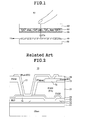
- FIG. 1 illustrates an LCD device with a built-in touch screen according to the related art, and a method for driving the same.
- the LCD device with a built-in touch screen comprises lower and upper substrates 50 and 60 bonded to each other with a liquid crystal layer (not shown) interposed therebetween.
- the black matrix 62 defines a pixel region corresponding to each of plural pixels.
- the red, green, and blue color filters 64R, 64G, and 64B are respectively formed in the respective pixel regions defined by the black matrix 62.
- the overcoat layer 66 covers the red, green, and blue color filters 64R, 64G, and 64B and the black matrix 62, to thereby planarize the upper substrate 60.
- a pixel array 40 including plural pixels to drive the liquid crystal layer and detect a touching point by finger or pen.
- Each of the plural pixels is defined by gate and data lines crossing each other. At the crossing portion of the gate and data lines, there is a thin film transistor (hereinafter, referred to as 'TFT'). Each of the plural pixels includes a common electrode and a pixel electrode.
- the in-cell touch type LCD device refers to an LCD device that uses an element existing in the related art structure as a touch-sensing electrode (for example, a common electrode Vcom may be used as a touch-sensing electrode).
- FIG. 2 is a cross section view illustrating a lower substrate in the LCD device with a built-in touch screen according to the related art.
- FIG. 2 shows a common electrode formed in the X-axis direction among all common electrodes of the LCD device.
- a common electrode 75 of a lower substrate 50 not only supplies a common voltage (Vcom), but also functions as a sensing electrode for detection a user's touch.
- Vcom common voltage
- the common electrodes (sensing electrode) 75 are formed in the X-axis and Y-axis directions.
- the common electrode 75 in the X-axis direction is brought into contact with a gate metal 73 at a lower portion of the lower substrate 50 through a contact structure, to be described.
- each pixel of the lower substrate 50 includes a buffer layer 51 on a glass substrate; a gate insulating layer 52; the gate metal 73; an interlayer dielectric (ILD) 53; a contact metal 74; a first passivation layer (PAS0) 54; a second passivation layer (PAS1) 55; the common electrode (Vcom) 75; a conductive line (3 rd metal) 76; a third passivation layer (PAS2) 56; and a contact electrode 77.
- ILD interlayer dielectric
- the first to third passivation layers (PAS0 to PAS2) 54 to 56 are partially etched to thereby form a contact hole for exposing a predetermined portion of the contact metal 74.
- the third passivation layer (PAS2) 56 is additionally etched to expose the conductive line 76.
- the gate metal 73 is formed of metal used for forming gate line.
- the contact metal 74 is formed of metal used for forming source and drain electrodes of TFT.
- the contact electrode 77 is formed of a transparent conductive material used for a pixel electrode (for example, ITO). Also, the contact electrode 77 is formed simultaneously with the pixel electrode.
- the contact hole for exposing the contact metal 74 is formed in the contact electrode 77. Also, the conductive line 76 is exposed by etching the third passivation layer 56 thereabove.
- the contact electrode 77 is formed inside the contact hole and simultaneously on the third passivation layer (PAS2) 56. Thus, the contact electrode 77 is electrically connected with the contact metal 74 and the conductive line 76.
- PAS2 third passivation layer
- the common electrode 75 in the X-axis direction is brought into contact with the gate metal 73.
- the contact electrode 77 is formed simultaneously with the pixel electrode.
- an aperture ratio of the corresponding pixel with the contact structure is relatively lower than that of the other pixels.
- the conductive line 76 is connected with the contact electrode 77, and the contact metal 74 connected with the gate metal 73 is connected with the contact electrode 77.
- This double contact structure may cause the structural problem of the increased size of the contact portion.
- the aperture ratio in the pixel with the contact structure is lowered by the increased size of the contact portion.
- the contact structure using the transparent metal of the pixel electrode is used so that an aperture ratio of the corresponding pixel is about 80% as compared to that of the neighboring pixels.
- the pixel with the contact structure may be shown as a dark point when a viewer watches the corresponding pixel with the contact structure, to thereby lower visibility.
- a picture quality of the LCD device is deteriorated.
- the double contact structure may cause the complicated manufacturing process and low manufacturing efficiency.
- the present invention is directed to an LCD device and a method for manufacturing the same that substantially obviates one or more problems due to limitations and disadvantages of the related art.
- An aspect of the present invention is to provide an LCD device and a method for manufacturing the same, which facilitates to realize high aperture ratio in a pixel with a contact structure between a gate metal and a conductive line for connection of a touch-sensing electrode (common electrode).
- Another aspect of the present invention is to provide an LCD device and a method for manufacturing the same, which facilitates to improve manufacturing efficiency owing to a simplified process of a lower substrate.
- a liquid crystal display device with a built-in touch screen which uses a common electrode as a touch-sensing electrode, comprising an intersection of a gate line and a data line to define a pixel region, a gate metal disposed in a central portion of the pixel, an insulating layer formed on the gate metal, a first contact hole disposed through the insulating layer to expose a predetermined portion of an upper surface of the gate metal, a contact metal on the insulating layer and inside the first contact hole, the contact metal electrically connected with the gate metal, a first passivation layer on the contact metal, a second contact hole disposed through the first passivation layer to expose a predetermined portion of an upper surface of the contact metal, a common electrode on the first passivation layer and inside the second contact hole, a conductive line electrically connected with the common electrode, and a second passivation layer on the first passivation
- a method for manufacturing a liquid crystal display device with a built-in touch screen which uses a common electrode as a touch-sensing electrode, comprising the steps of forming a pixel region defined by an intersection of a gate line and a data line, forming a gate metal disposed in a central portion of the pixel, forming an insulating layer on the gate metal, a first contact hole disposed through the insulating layer to expose a predetermined portion of an upper surface of the gate metal, forming a contact metal on the insulating layer and inside the first contact hole, the contact metal electrically connected with the gate metal, forming a first passivation layer on the contact metal, a second contact hole disposed through the first passivation layer to expose a predetermined portion of an upper surface of the contact metal, forming a common electrode on the first passivation layer and inside the second contact hole, forming a conductive line electrically connected with the common electrode, and forming a second passivation layer on
- a method for manufacturing an liquid crystal display device with a built-in touch screen comprising forming a first contact hole by etching a predetermined portion of an insulating layer on a gate metal, wherein the first contact hole exposes a predetermined portion of an upper surface of the gate metal, forming a contact metal on the insulating layer and inside the first contact hole, wherein the contact metal is electrically connected with the gate metal, forming a first passivation layer on the contact metal, and forming a second contact hole by etching a predetermined portion of the first passivation layer, wherein the second contact hole exposes a predetermined portion of an upper surface of the contact metal, forming a common electrode on the first passivation layer and inside the second contact hole, forming a conductive line inside the second contact hole, wherein the conductive line is electrically connected with the common electrode, and forming a second passivation layer on the first passivation layer and the conductive line, wherein the gate metal and the common
- FIG. 1 illustrates an LCD device with a built-in touch screen according to the related art, and a method for manufacturing the same;
- FIG. 2 is a cross section view illustrating a lower substrate in an LCD device with a built-in touch screen according to the related art
- FIGs. 3 and 4 illustrate an LCD device with a built-in touch screen according to the first embodiment of the present invention
- FIGs. 5 and 6 illustrate an LCD device with a built-in touch screen according to the second embodiment of the present invention
- FIG. 7 illustrates an LCD device with a built-in touch screen according to the third embodiment of the present invention.
- FIGs. 8A-8D illustrate a method for manufacturing an LCD device with a built-in touch screen according to the embodiment of the present invention.
- first structure for example, electrode, line, layer, contact, and etc.
- first and second structures may come in contact with each other, or there may be a third structure interposed between the first and second structures.
- an LCD device may be classified into Twisted-Nematic (TN) mode, Vertical-Alignment (VA) mode, In-Plane Switching (IPS) mode, and Fringe Field Switching (FFS) mode.
- TN Twisted-Nematic
- VA Vertical-Alignment
- IPS In-Plane Switching
- FFS Fringe Field Switching
- both a pixel electrode and a common electrode are formed on a lower substrate, whereby liquid crystal molecules of the liquid crystal layer are aligned depending on an electric field between the pixel electrode and the common electrode.
- the pixel electrode and the common electrode are alternately arranged in parallel so that an In-Plane mode electric field occurs between the pixel electrode and the common electrode, thereby aligning the liquid crystal molecules of the liquid crystal layer.
- the liquid crystal molecules are not properly aligned above the pixel electrode and the common electrode, whereby light transmittance is relatively deteriorated above the pixel electrode and the common electrode.
- the FFS mode has been proposed.
- an insulating layer is interposed between the pixel electrode and the common electrode, whereby the pixel electrode is formed at a predetermined interval from the common electrode by the interposed insulating layer.
- any one of the pixel electrode and the common electrode is formed in a plate shape or pattern, and the other is formed in a finger shape, whereby a fringe field occurs between the pixel electrode and the common electrode.
- the liquid crystal molecules of the liquid crystal layer are aligned by the fringe field occurring between the pixel electrode and the common electrode.
- the LCD device with a built-in touch screen according to the embodiment of the present invention is formed in the FFS mode.
- the LCD device with a built-in touch screen comprises an in-cell touch type liquid crystal panel with a built-in touch screen for detection of a user's touch point; a backlight unit for supplying light to the liquid crystal panel; and a driving circuit.
- a contact structure between a gate metal and a common electrode driven as a touch-sensing electrode is a main point in this present invention.
- a detailed explanation for the driving circuit and the backlight unit will be omitted.
- the LCD device with a built-in touch screen displays an image according to a video signal by controlling transmittance of light passing through a liquid crystal layer in each pixel.
- the common electrode on the lower substrate is driven as the touch-sensing electrode so as to sense the change of capacitance depending on a user's touch, and to detect the user's touch.
- BM black matrix
- red, green, and blue color filters red, green, and blue color filters
- overcoat layer an overcoat layer
- a pixel array including plural pixels to drive the liquid crystal layer and detect the touching point by sensing the capacitance depending on the user's touch.
- the pixel array includes gate and data lines crossing each other to defme the pixel; a common electrode; and a conductive line for connection of the common electrodes of the neighboring pixels. Also, a thin film transistor (TFT) serving as a switching element is formed in each pixel, and is connected with a pixel electrode.
- TFT thin film transistor
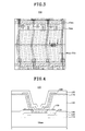
- FIGs. 3 and 4 illustrate an LCD device with a built-in touch screen according to the first embodiment of the present invention.
- FIG. 4 is a cross section view along I-I' of FIG. 3 .
- FIGs. 3 and 4 show a contact portion between a gate metal and a common electrode in an entire pixel region of a lower substrate.
- the contact structure between the gate metal and the common electrode has an overlap portion, to thereby realize high aperture ratio in the corresponding pixel with the contact structure of common electrode.
- a buffer layer 110 on the lower substrate 100, there are a buffer layer 110; a gate insulating layer (GI) 120; a gate metal 130; an interlayer dielectric (ILD) 140; a contact metal 150; a first passivation layer (PAS1) 160; a common electrode (Vcom) 170; a conductive line 180; and a second passivation layer (PAS2) 190.
- GI gate insulating layer
- ILD interlayer dielectric
- the buffer layer 110 and the gate insulating layer 120 are sequentially formed on a glass substrate. Then, the gate metal 130 is formed on the gate insulating layer 120.
- the gate metal 130 is formed of metal used for forming the gate line, wherein the gate metal 130 is positioned in the central portion of the pixel.
- an active layer (semiconductor layer) is formed below the gate insulating layer 120 of a TFT region. Also, a channel of the TFT is formed in an overlap region between the active layer and a gate electrode diverged from the gate line.
- TEOS Tetra Ethyl Ortho Silicate
- MTO Middle Temperature Oxide
- a predetermined portion of an upper surface of the gate metal 130 is exposed by etching a predetermined portion of the interlayer dielectric 140. Also, predetermined portions of the contact metal 150, positioned on the interlayer dielectric 140, are overlapped with the gate metal 130.
- the contact metal 150 is electrically connected with the gate metal 130.
- the contact metal 150 is brought into contact with the central portion of the gate metal 130. That is, the gate metal 130 is overlapped with the contact metal 150.
- the contact metal 150 may be formed of metal used for formation of source and drain electrodes of the TFT. Also, the contact metal 150 may be formed simultaneously with the source and drain electrodes of the TFT.
- the first passivation layer (PAS 1) 160 is formed on the interlayer dielectric 140 and the contact metal 150. A predetermined portion of an upper surface of the contact metal 150 is exposed by partially etching the first passivation layer (PAS1) 160 above the contact portion between the gate metal 130 and the contact metal 150.
- the common electrode 170 is formed of a transparent conductive material such as ITO.
- the common electrode 170 is formed on the first passivation layer (PAS 1) 160, and simultaneously formed inside the contact hole obtained by partially etching the first passivation layer (PAS1) 160. Inside the contact hole, the contact metal 150 is electrically connected with the common electrode 170.
- the common electrode 170 supplies the common voltage for controlling the transmittance of light passing through the liquid crystal layer to the pixel.
- the common electrode 170 is driven as the touch-sensing electrode to detect the change of capacitance (Ctc) depending on the user's touch.
- the common electrode of the LCD device according to the related art is formed in a plate shape to supply the same common voltage (Vcom) to the entire pixel region of the lower substrate.
- the common electrode 170 of the LCD device according to the first embodiment of the present invention not only supplies the common voltage (Vcom), but also functions as the touch-sensing electrode for detection the user's touch.
- the common electrode 170 is patterned every individual pixel.
- the common electrode 170 may be patterned every predetermined number of the pixels.
- the common electrodes of the neighboring pixels may be connected via the conductive line 180 by the X-axis direction or Y-axis direction. At this time, the common electrodes of the X-axis direction are brought into contact with the gate metal 130 through the aforementioned contact structure.
- the conductive line 180 is formed by depositing (burying) a metal material on the first passivation layer (PAS 1) 160 and inside the contact hole obtained by etching the first passivation layer (PAS1) 160. The conductive line 180 is brought into contact with the common electrode 170.
- the conductive line 180 may be formed as the contact line to make the common electrode 170 driven as the touch-sensing electrode for detection of the user's touch.
- the second passivation layer (PAS2) 190 is formed to cover the common electrode 170 and the conductive line 180.
- the above LCD device with a built-in touch screen according to the first embodiment of the present invention has the contact structure where the gate metal 130, the contact metal 150, the common electrode 170, and the conductive line 180 are overlapped with one another in the same vertical line.
- the conductive line is firstly brought into contact with the pixel electrode by the use of pixel electrode, and then the pixel electrode is secondly brought into contact with the contact electrode, to thereby make the double contact structure.
- the aperture ratio may be lowered in the corresponding pixel with the contact structure.
- the gate metal 130 is directly brought into contact with the common electrode 170 while being overlapped with the common electrode 170 in the same vertical line, to thereby realize the high aperture ratio.
- the above contact structure is formed in the central portion of disclination in the multi-domain pixel structure, whereby the aperture ratio of the corresponding pixel is increased to be about 90% as compared to that of the neighboring pixels (wherein, the neighboring pixel indicates the pixel without the contact structure).
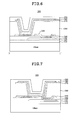
- FIGs. 5 and 6 illustrate an LCD device with a built-in touch screen according to the second embodiment of the present invention.
- FIG. 6 is a cross section view along II-II' of FIG. 5 .
- FIGs. 5 and 6 show a contact portion between a gate metal and a common electrode in an entire pixel region of a lower substrate.
- the LCD device according to the second embodiment of the present invention is identical in structure to the LCD device according to the first embodiment of the present invention.
- a contact structure between a gate metal and a common electrode has an overlap portion, thereby increasing aperture ratio of the pixel with the contact structure, and reducing step coverage by the overlap portion of the contact structure.
- a buffer layer 110 on a lower substrate 200, there are a buffer layer 110; a gate insulating layer (GI) 120; a gate metal 130; an interlayer dielectric (ILD) 240; a contact metal 250; a first passivation layer (PAS1) 260; a common electrode (Vcom) 270; a conductive line (3 rd metal) 280; and a second passivation layer (PAS2) 290.
- GI gate insulating layer
- ILD interlayer dielectric
- the interlayer dielectric (ILD) 240 is formed to cover the gate metal 130. A predetermined portion of an upper surface of the gate metal 130 is exposed by partially etching a predetermined portion of the interlayer dielectric 240.
- the contact metal 250 is overlapped with the gate metal 130 above the interlayer dielectric 240. In the exposed portion of the gate metal 130, the contact metal 250 is electrically connected with the gate metal 130. At this time, the contact portion between the gate metal 130 and the contact metal 250 is provided at one side with respect to the central portion of the gate metal 130.
- the contact metal 250 may be formed of metal used for formation of source and drain electrodes of the TFT. Also, the contact metal 250 may be formed simultaneously with the source and drain electrodes of the TFT.
- the gate metal 130 is overlapped with the contact metal 250.
- the first passivation layer (PAS 1) 260 is formed on the interlayer dielectric 240 and the contact metal 250.
- a contact hole is formed by etching a predetermined portion of the first passivation layer 260. Via this contact hole, a predetermined portion of an upper surface of the contact metal 250 is exposed. In this case, the predetermined portion of the first passivation layer 260, which is not overlapped with the contact portion between the gate metal 130 and the contact metal 250, is etched.
- the common electrode 270 is formed on the first passivation layer (PAS1) 260, and is also formed inside the contact hole realized by etching the first passivation layer (PAS1) 260. Inside the contact hole, the contact metal 250 is electrically connected with the common electrode 270.
- the common electrodes of the neighboring pixels may be connected via the conductive line 280 by the X-axis direction or Y-axis direction. At this time, the common electrodes of the X-axis direction are brought into contact with the gate metal 130 through the aforementioned contact structure.
- the conductive line 280 is formed by depositing (burying) a metal material on the first passivation layer (PAS1) 260 and inside the contact hole obtained by etching the first passivation layer (PAS1) 260.
- the conductive line 280 is brought into contact with the common electrode 270.
- the conductive line 280 may be formed as the contact line to make the common electrode 270 driven as the touch-sensing electrode for detection of the user's touch.
- the second passivation layer (PAS2) 290 is formed to cover the common electrode 270 and the conductive line 280.
- the gate metal and the common electrode are brought into contact with each other via the contact metal, wherein the gate metal, the common electrode, and the contact metal are overlapped in the same vertical line.
- the contact portion between the gate metal 130 and the contact metal 250, and the contact portion between the contact metal 250 and the common electrode 270 are provided at the different vertical lines.
- the aperture ratio of the pixel may be increased owing to the contact between the gate metal 130 and the common electrode 270 via the contact metal 250. Also, it is possible to reduce the step coverage caused by the contact structure.
- the contact structure is formed in the central portion of disclination in the multi-domain pixel structure, thereby realizing the high aperture ratio in the corresponding pixel.
- FIG. 7 illustrates an LCD device with a built-in touch screen according to the third embodiment of the present invention.
- FIG. 7 shows a contact portion between a gate metal and a common electrode in an entire pixel region of a lower substrate.
- the LCD device according to the third embodiment of the present invention is identical in structure to the LCD device according to the first embodiment of the present invention.
- a contact structure between a gate metal and a common electrode has an overlap portion, thereby increasing aperture ratio of the pixel with the contact structure, and reducing step coverage by the overlap portion of the contact structure.
- a buffer layer 110 on a lower substrate 300, there are a buffer layer 110; a gate insulating layer (GI) 120; a gate metal 130; an interlayer dielectric (ILD) 340; a contact metal 350; a first passivation layer (PAS1) 360; a common electrode (Vcom) 370; a conductive line 380; and a second passivation layer (PAS2) 390.
- GI gate insulating layer
- ILD interlayer dielectric
- PAS1 first passivation layer
- Vcom common electrode
- conductive line 380 a conductive line 380
- PAS2 second passivation layer
- the interlayer dielectric (ILD) 340 is formed to cover the gate metal 130. A predetermined portion of an upper surface of the gate metal 130 is exposed by partially etching a predetermined portion of the interlayer dielectric 340.
- the contact metal 350 is overlapped with the gate metal 130 above the interlayer dielectric 340. In the exposed portion of the gate metal 130, the contact metal 350 is electrically connected with the gate metal 130. At this time, the contact portion between the gate metal 130 and the contact metal 350 is positioned at one side with respect to the central portion of the gate metal 130.
- the contact metal 350 may be formed of metal used for formation of source and drain electrodes of the TFT.
- the gate metal 130 is overlapped with the contact metal 350.
- the first passivation layer (PAS1) 360 is formed on the interlayer dielectric 340 and the contact metal 350.
- a contact hole is formed by etching a predetermined portion of the first passivation layer 360.
- a predetermined portion of an upper surface of the contact metal 350 is exposed through the contact hole.
- the etched portion of the first passivation layer (PAS1) 360 is partially overlapped with the contact portion between the gate metal 130 and the contact metal 350.
- the common electrode 370 is formed on the first passivation layer (PAS1) 360, and is formed inside the contact hole obtained by etching the first passivation layer (PAS1) 360. Inside the contact hole, the contact metal 350 is electrically connected with the common electrode 370.
- the common electrodes 370 of the neighboring pixels are connected via the conductive line 370 by the X-axis direction or Y-axis direction.
- the common electrodes 370 of the X-axis direction are brought into contact with the gate metal 130 through the above contact structure.
- the conductive line 380 is formed by depositing (burying) a metal material on the first passivation layer (PAS1) 360 and inside the contact hole obtained by etching the first passivation layer (PAS1) 360. The conductive line 380 is brought into contact with the common electrode 370.
- the conductive line 380 may be formed as the contact line to make the common electrode 370 driven as the touch-sensing electrode for detection of the user's touch.
- the second passivation layer (PAS2) 390 is formed to cover the common electrode 370 and the conductive line 380.
- the above LCD device with a built-in touch screen according to the first embodiment of the present invention has the contact structure where the gate metal and the common electrode are overlapped with each other in the same vertical line.
- the LCD device with a built-in touch screen according to the third embodiment of the present invention has the contact structure where the contact portion between the gate metal 130 and the contact metal 350 is partially overlapped with the contact portion between the contact metal 350 and the common electrode 370 in the vertical line.
- the aperture ratio of the pixel may be increased owing to the contact between the gate metal 130 and the common electrode 370 through the contact metal 350. Also, it is possible to reduce the step coverage caused by the contact structure.
- the contact structure is formed in the central portion of disclination in the multi-domain pixel structure, thereby realizing the high aperture ratio in the corresponding pixel.
- the LCD devices according to the first to third embodiments of the present invention provides the good visibility of the pixel and good display quality by improving the contact structure between the gate metal and the common electrode.
- FIG. 8 illustrates a method for manufacturing the LCD device according to the first embodiment of the present invention.
- the buffer layer 110 is formed on the substrate. Then, TEOS (Tetra Ethyl Ortho Silicate) or MTO (Middle Temperature Oxide) may be deposited on an entire surface of the substrate, to thereby form the gate insulating layer 120.
- TEOS Tetra Ethyl Ortho Silicate
- MTO Middle Temperature Oxide
- a metal material is deposited on the gate insulating layer 120, and then photolithography and dry-etching process using a mask is applied to the deposited metal material, to thereby form the gate metal 130.
- the substrate may be formed of glass or plastic material.
- FIGs. 8A-8D show the exemplary case using the glass substrate.
- an insulating material is deposited on the substrate to cover the gate metal 130 and the gate insulating layer 120, thereby forming the interlayer dielectric (ILD) 140.
- ILD interlayer dielectric
- photolithography and dry-etching process using a mask is carried out to etch a predetermined portion of the interlayer dielectric 140, thereby forming the first contact hole for exposing the upper surface of the central portion of the gate metal 130.
- a metal material is deposited to cover the interlayer dielectric 140, and photolithography and wet-etching process using a mask is applied to the deposited metal material, to thereby form the contact metal 150.
- the contact metal 150 is formed by the process for forming the source and drain electrodes of the TFT, and is simultaneously with the source and drain electrodes of the TFT.
- the gate metal 130 and the contact metal 150 are electrically connected with each other inside the first contact hole obtained by etching the interlayer dielectric 140.
- the first passivation layer (PAS1) 160 is formed to cover the interlayer dielectric 140 and the contact metal 150, and then photolithography and etching process is applied thereto, to thereby form the second contact hole.
- the second contact hole is formed in the contact portion between the gate metal 130 and the contact metal 150.
- a transparent conductive material such as ITO is deposited on the first passivation layer (PAS 1) 160, and is formed inside the second contact hole, to thereby form the common electrode (Vcom) 170.
- the gate metal 130 and the common electrode 170 are electrically connected with each other via the contact metal 150 inside the second contact hole.
- a conductive metal material is deposited on the common electrode 170, and photolithography and etching process using a mask is applied to the deposited conductive metal material, to thereby form the conductive line 180 electrically connected with the common electrode 170.
- the second passivation layer (PAS2) 190 is formed to cover the common electrode 170 and the conductive line 180.
- the gate metal and the common electrode are overlapped in the same vertical line, to thereby realize the high aperture ratio in the pixel with the contact structure.
- the passivation layer PAS0 which has been applied to the related art structure, is omitted so that the contact structure and the manufacturing process are simplified, thereby improving the manufacturing efficiency and price competition of the LCD device with a built-in touch screen according to the present invention.
- the method for manufacturing the LCD device with a built-in touch screen according to another embodiment of the present invention the first contact hole and the second contact hole, which are formed by the processes of FIG. 8B and FIG. 8C , are not overlapped with each other, to thereby form the contact structure according to the second embodiment of the present invention, as shown in FIG. 6 .
- the contact structure according to the third embodiment of the present invention may be obtained by partially overlapping the first and second contact holes, as shown in FIG. 7 .
- the LCD device has the contact structure where the touch-sensing electrode (common electrode) is brought into contact with the gate metal, to thereby improve the display quality owing to the high aperture ratio of the pixel.
- the contact structure between the common electrode and the gate metal is formed in the central portion of disclination in the multi-domain pixel structure, thereby realizing the high aperture ratio in the corresponding pixel.
- the simplified manufacturing process of the lower substrate in the LCD device according to the present invention enables to reduce the manufacturing cost of the LCD device, and to improve the manufacturing efficiency.
Landscapes
- Engineering & Computer Science (AREA)
- Physics & Mathematics (AREA)
- Theoretical Computer Science (AREA)
- General Engineering & Computer Science (AREA)
- General Physics & Mathematics (AREA)
- Nonlinear Science (AREA)
- Human Computer Interaction (AREA)
- Crystallography & Structural Chemistry (AREA)
- Chemical & Material Sciences (AREA)
- Optics & Photonics (AREA)
- Mathematical Physics (AREA)
- Microelectronics & Electronic Packaging (AREA)
- Liquid Crystal (AREA)
Applications Claiming Priority (1)
| Application Number | Priority Date | Filing Date | Title |
|---|---|---|---|
| KR1020100092392A KR101284714B1 (ko) | 2010-09-20 | 2010-09-20 | 액정 표시장치와 이의 제조방법 |
Publications (2)
| Publication Number | Publication Date |
|---|---|
| EP2431802A1 true EP2431802A1 (de) | 2012-03-21 |
| EP2431802B1 EP2431802B1 (de) | 2017-12-06 |
Family
ID=44650885
Family Applications (1)
| Application Number | Title | Priority Date | Filing Date |
|---|---|---|---|
| EP11007618.9A Active EP2431802B1 (de) | 2010-09-20 | 2011-09-19 | Flüssigkristallanzeigevorrichtung und Herstellungsverfahren dafür |
Country Status (5)
| Country | Link |
|---|---|
| US (1) | US8792060B2 (de) |
| EP (1) | EP2431802B1 (de) |
| KR (1) | KR101284714B1 (de) |
| CN (1) | CN102411238B (de) |
| TW (1) | TWI448776B (de) |
Cited By (1)
| Publication number | Priority date | Publication date | Assignee | Title |
|---|---|---|---|---|
| CN106200077A (zh) * | 2016-08-31 | 2016-12-07 | 深圳市华星光电技术有限公司 | 一种触控面板及其制作方法 |
Families Citing this family (17)
| Publication number | Priority date | Publication date | Assignee | Title |
|---|---|---|---|---|
| US9720295B2 (en) | 2011-09-27 | 2017-08-01 | Lg Display Co., Ltd. | Liquid crystal display device and method for manufacturing the same |
| CN103135815B (zh) * | 2011-11-25 | 2017-02-22 | 上海天马微电子有限公司 | 内嵌触摸屏液晶显示装置及其触控驱动方法 |
| JP2015187754A (ja) * | 2012-08-09 | 2015-10-29 | シャープ株式会社 | 液晶表示装置 |
| KR102017204B1 (ko) | 2012-11-01 | 2019-09-03 | 삼성디스플레이 주식회사 | 박막 트랜지스터 표시판 및 그 제조 방법 |
| TWI607542B (zh) * | 2012-11-22 | 2017-12-01 | Lg伊諾特股份有限公司 | 觸控視窗 |
| JP6253923B2 (ja) * | 2013-08-30 | 2017-12-27 | 株式会社ジャパンディスプレイ | タッチセンサ内蔵有機エレクトロルミネッセンス装置 |
| US9543335B2 (en) | 2014-07-17 | 2017-01-10 | Innolux Corporation | Liquid-crystal display and element substrate thereof |
| TWI567452B (zh) * | 2014-07-17 | 2017-01-21 | 群創光電股份有限公司 | 液晶顯示裝置及其元件基板 |
| CN104461142B (zh) * | 2014-12-10 | 2017-06-30 | 京东方科技集团股份有限公司 | 触控显示基板及其制备方法、触控显示装置 |
| KR101727108B1 (ko) * | 2014-12-31 | 2017-04-17 | 엘지디스플레이 주식회사 | 인셀 터치 액정 디스플레이 장치와 이의 제조방법 |
| CN104503647B (zh) * | 2014-12-31 | 2017-12-08 | 京东方科技集团股份有限公司 | 一种触摸显示屏的基板及其制造方法、触摸屏及显示装置 |
| CN104698665B (zh) | 2015-04-01 | 2017-11-07 | 上海天马微电子有限公司 | 触控显示面板结构及其形成方法、触控显示装置 |
| CN106873267B (zh) * | 2015-12-14 | 2021-02-19 | 群创光电股份有限公司 | 显示面板 |
| CN106896609B (zh) * | 2017-04-28 | 2019-11-19 | 厦门天马微电子有限公司 | 一种阵列基板及包括其的显示装置 |
| CN107402671B (zh) * | 2017-06-19 | 2020-03-17 | 南京中电熊猫液晶显示科技有限公司 | 一种内嵌式触控面板及其制造方法 |
| US11402942B2 (en) * | 2020-03-24 | 2022-08-02 | Beijing Boe Display Technology Co., Ltd. | Array substrate and display device |
| KR20230011079A (ko) | 2021-07-13 | 2023-01-20 | (주)에이케이테크 | 합성수지로 만들어지는 모터용 고정자 및 이에 사용하기 위한 와이어 |
Citations (3)
| Publication number | Priority date | Publication date | Assignee | Title |
|---|---|---|---|---|
| WO2010084642A1 (ja) * | 2009-01-26 | 2010-07-29 | シャープ株式会社 | 表示装置内蔵型タッチパネル |
| EP2214084A1 (de) * | 2009-02-02 | 2010-08-04 | Apple Inc. | Integrierter Berührungsbildschirm |
| KR20100092392A (ko) | 2009-02-12 | 2010-08-20 | 제록스 코포레이션 | 유기 아민 안정화 은 나노입자 및 그의 제조 방법 |
Family Cites Families (8)
| Publication number | Priority date | Publication date | Assignee | Title |
|---|---|---|---|---|
| KR101211345B1 (ko) | 2005-12-14 | 2012-12-11 | 엘지디스플레이 주식회사 | 액정표시장치 및 그 제조방법 |
| CN100426511C (zh) * | 2006-06-23 | 2008-10-15 | 北京京东方光电科技有限公司 | 一种薄膜晶体管器件阵列基板结构及其制造方法 |
| KR20080052836A (ko) * | 2006-12-08 | 2008-06-12 | 삼성전자주식회사 | 액정 표시 장치 및 그 제조 방법 |
| EP2120136A4 (de) | 2007-03-01 | 2013-01-23 | Sharp Kk | Anzeigeschirmsubstrat, anzeigeschirm, anzeigeanordnung und verfahren zur herstellung eines anzeigeschirmsubstrats |
| JP5207163B2 (ja) * | 2007-03-30 | 2013-06-12 | Nltテクノロジー株式会社 | 埋込配線の形成方法、表示装置用基板及び当該基板を有する表示装置 |
| TWI384277B (zh) * | 2007-09-07 | 2013-02-01 | Japan Display West Inc | 液晶顯示裝置 |
| KR101564332B1 (ko) * | 2008-10-28 | 2015-10-30 | 삼성전자주식회사 | 액정 표시 장치에 일체화된 터치 스크린 패널과 그 제조 방법 및 터치 센싱 방법 |
| JP5140018B2 (ja) | 2009-02-24 | 2013-02-06 | 株式会社ジャパンディスプレイイースト | 入力機能付き液晶表示装置 |
-
2010
- 2010-09-20 KR KR1020100092392A patent/KR101284714B1/ko active Active
-
2011
- 2011-08-04 US US13/198,175 patent/US8792060B2/en active Active
- 2011-08-09 TW TW100128396A patent/TWI448776B/zh active
- 2011-09-02 CN CN201110263524.6A patent/CN102411238B/zh active Active
- 2011-09-19 EP EP11007618.9A patent/EP2431802B1/de active Active
Patent Citations (3)
| Publication number | Priority date | Publication date | Assignee | Title |
|---|---|---|---|---|
| WO2010084642A1 (ja) * | 2009-01-26 | 2010-07-29 | シャープ株式会社 | 表示装置内蔵型タッチパネル |
| EP2214084A1 (de) * | 2009-02-02 | 2010-08-04 | Apple Inc. | Integrierter Berührungsbildschirm |
| KR20100092392A (ko) | 2009-02-12 | 2010-08-20 | 제록스 코포레이션 | 유기 아민 안정화 은 나노입자 및 그의 제조 방법 |
Cited By (1)
| Publication number | Priority date | Publication date | Assignee | Title |
|---|---|---|---|---|
| CN106200077A (zh) * | 2016-08-31 | 2016-12-07 | 深圳市华星光电技术有限公司 | 一种触控面板及其制作方法 |
Also Published As
| Publication number | Publication date |
|---|---|
| US8792060B2 (en) | 2014-07-29 |
| TWI448776B (zh) | 2014-08-11 |
| KR101284714B1 (ko) | 2013-07-17 |
| TW201213944A (en) | 2012-04-01 |
| KR20120030709A (ko) | 2012-03-29 |
| CN102411238A (zh) | 2012-04-11 |
| CN102411238B (zh) | 2014-10-29 |
| EP2431802B1 (de) | 2017-12-06 |
| US20120068200A1 (en) | 2012-03-22 |
Similar Documents
| Publication | Publication Date | Title |
|---|---|---|
| EP2431802B1 (de) | Flüssigkristallanzeigevorrichtung und Herstellungsverfahren dafür | |
| EP2431847B1 (de) | Flüssigkristallanzeigevorrichtung mit integriertem Berührungsbildschirm und Verfahren zur deren Herstellung | |
| US9218082B2 (en) | Liquid crystal display device with a built-in touch screen and method for manufacturing the same | |
| US10310345B2 (en) | In-cell touch liquid crystal display apparatus, method of manufacturing the same, method of manufacturing thin film transistor array substrate, and method of manufacturing color filter array substrate | |
| US9971181B2 (en) | In-cell touch liquid crystal display device and method for manufacturing the same | |
| US8698971B2 (en) | Liquid crystal display device and method for manufacturing the same | |
| US8878814B2 (en) | Liquid crystal display device provided with a sensing electrode for sensing a touch of a user | |
| US9036105B2 (en) | Liquid crystal display device and method of manufacturing the same | |
| US8982064B2 (en) | Liquid crystal display device provided with a sensing electrode for sending a touch of a user | |
| US8743301B2 (en) | Liquid crystal display device provided with an electrode for sensing a touch of a user | |
| US8792061B2 (en) | Liquid crystal display device | |
| CN105739203B (zh) | 内嵌式触摸液晶显示装置及其制造方法 | |
| KR101810503B1 (ko) | 터치 스크린이 내장된 액정 표시장치 | |
| KR101705557B1 (ko) | 터치 스크린이 내장된 액정 표시장치 |
Legal Events
| Date | Code | Title | Description |
|---|---|---|---|
| PUAI | Public reference made under article 153(3) epc to a published international application that has entered the european phase |
Free format text: ORIGINAL CODE: 0009012 |
|
| AK | Designated contracting states |
Kind code of ref document: A1 Designated state(s): AL AT BE BG CH CY CZ DE DK EE ES FI FR GB GR HR HU IE IS IT LI LT LU LV MC MK MT NL NO PL PT RO RS SE SI SK SM TR |
|
| AX | Request for extension of the european patent |
Extension state: BA ME |
|
| 17P | Request for examination filed |
Effective date: 20120914 |
|
| 17Q | First examination report despatched |
Effective date: 20150225 |
|
| GRAP | Despatch of communication of intention to grant a patent |
Free format text: ORIGINAL CODE: EPIDOSNIGR1 |
|
| GRAJ | Information related to disapproval of communication of intention to grant by the applicant or resumption of examination proceedings by the epo deleted |
Free format text: ORIGINAL CODE: EPIDOSDIGR1 |
|
| GRAP | Despatch of communication of intention to grant a patent |
Free format text: ORIGINAL CODE: EPIDOSNIGR1 |
|
| INTG | Intention to grant announced |
Effective date: 20170703 |
|
| INTG | Intention to grant announced |
Effective date: 20170713 |
|
| RAP1 | Party data changed (applicant data changed or rights of an application transferred) |
Owner name: LG DISPLAY CO., LTD. |
|
| GRAS | Grant fee paid |
Free format text: ORIGINAL CODE: EPIDOSNIGR3 |
|
| GRAA | (expected) grant |
Free format text: ORIGINAL CODE: 0009210 |
|
| AK | Designated contracting states |
Kind code of ref document: B1 Designated state(s): AL AT BE BG CH CY CZ DE DK EE ES FI FR GB GR HR HU IE IS IT LI LT LU LV MC MK MT NL NO PL PT RO RS SE SI SK SM TR |
|
| REG | Reference to a national code |
Ref country code: GB Ref legal event code: FG4D |
|
| REG | Reference to a national code |
Ref country code: AT Ref legal event code: REF Ref document number: 952893 Country of ref document: AT Kind code of ref document: T Effective date: 20171215 Ref country code: CH Ref legal event code: EP |
|
| REG | Reference to a national code |
Ref country code: IE Ref legal event code: FG4D |
|
| REG | Reference to a national code |
Ref country code: DE Ref legal event code: R096 Ref document number: 602011043898 Country of ref document: DE |
|
| REG | Reference to a national code |
Ref country code: NL Ref legal event code: MP Effective date: 20171206 |
|
| REG | Reference to a national code |
Ref country code: LT Ref legal event code: MG4D |
|
| PG25 | Lapsed in a contracting state [announced via postgrant information from national office to epo] |
Ref country code: SE Free format text: LAPSE BECAUSE OF FAILURE TO SUBMIT A TRANSLATION OF THE DESCRIPTION OR TO PAY THE FEE WITHIN THE PRESCRIBED TIME-LIMIT Effective date: 20171206 Ref country code: LT Free format text: LAPSE BECAUSE OF FAILURE TO SUBMIT A TRANSLATION OF THE DESCRIPTION OR TO PAY THE FEE WITHIN THE PRESCRIBED TIME-LIMIT Effective date: 20171206 Ref country code: NO Free format text: LAPSE BECAUSE OF FAILURE TO SUBMIT A TRANSLATION OF THE DESCRIPTION OR TO PAY THE FEE WITHIN THE PRESCRIBED TIME-LIMIT Effective date: 20180306 Ref country code: ES Free format text: LAPSE BECAUSE OF FAILURE TO SUBMIT A TRANSLATION OF THE DESCRIPTION OR TO PAY THE FEE WITHIN THE PRESCRIBED TIME-LIMIT Effective date: 20171206 Ref country code: FI Free format text: LAPSE BECAUSE OF FAILURE TO SUBMIT A TRANSLATION OF THE DESCRIPTION OR TO PAY THE FEE WITHIN THE PRESCRIBED TIME-LIMIT Effective date: 20171206 |
|
| REG | Reference to a national code |
Ref country code: AT Ref legal event code: MK05 Ref document number: 952893 Country of ref document: AT Kind code of ref document: T Effective date: 20171206 |
|
| PG25 | Lapsed in a contracting state [announced via postgrant information from national office to epo] |
Ref country code: GR Free format text: LAPSE BECAUSE OF FAILURE TO SUBMIT A TRANSLATION OF THE DESCRIPTION OR TO PAY THE FEE WITHIN THE PRESCRIBED TIME-LIMIT Effective date: 20180307 Ref country code: RS Free format text: LAPSE BECAUSE OF FAILURE TO SUBMIT A TRANSLATION OF THE DESCRIPTION OR TO PAY THE FEE WITHIN THE PRESCRIBED TIME-LIMIT Effective date: 20171206 Ref country code: HR Free format text: LAPSE BECAUSE OF FAILURE TO SUBMIT A TRANSLATION OF THE DESCRIPTION OR TO PAY THE FEE WITHIN THE PRESCRIBED TIME-LIMIT Effective date: 20171206 Ref country code: LV Free format text: LAPSE BECAUSE OF FAILURE TO SUBMIT A TRANSLATION OF THE DESCRIPTION OR TO PAY THE FEE WITHIN THE PRESCRIBED TIME-LIMIT Effective date: 20171206 Ref country code: BG Free format text: LAPSE BECAUSE OF FAILURE TO SUBMIT A TRANSLATION OF THE DESCRIPTION OR TO PAY THE FEE WITHIN THE PRESCRIBED TIME-LIMIT Effective date: 20180306 |
|
| PG25 | Lapsed in a contracting state [announced via postgrant information from national office to epo] |
Ref country code: NL Free format text: LAPSE BECAUSE OF FAILURE TO SUBMIT A TRANSLATION OF THE DESCRIPTION OR TO PAY THE FEE WITHIN THE PRESCRIBED TIME-LIMIT Effective date: 20171206 |
|
| PG25 | Lapsed in a contracting state [announced via postgrant information from national office to epo] |
Ref country code: CZ Free format text: LAPSE BECAUSE OF FAILURE TO SUBMIT A TRANSLATION OF THE DESCRIPTION OR TO PAY THE FEE WITHIN THE PRESCRIBED TIME-LIMIT Effective date: 20171206 Ref country code: SK Free format text: LAPSE BECAUSE OF FAILURE TO SUBMIT A TRANSLATION OF THE DESCRIPTION OR TO PAY THE FEE WITHIN THE PRESCRIBED TIME-LIMIT Effective date: 20171206 Ref country code: EE Free format text: LAPSE BECAUSE OF FAILURE TO SUBMIT A TRANSLATION OF THE DESCRIPTION OR TO PAY THE FEE WITHIN THE PRESCRIBED TIME-LIMIT Effective date: 20171206 |
|
| PG25 | Lapsed in a contracting state [announced via postgrant information from national office to epo] |
Ref country code: RO Free format text: LAPSE BECAUSE OF FAILURE TO SUBMIT A TRANSLATION OF THE DESCRIPTION OR TO PAY THE FEE WITHIN THE PRESCRIBED TIME-LIMIT Effective date: 20171206 Ref country code: AT Free format text: LAPSE BECAUSE OF FAILURE TO SUBMIT A TRANSLATION OF THE DESCRIPTION OR TO PAY THE FEE WITHIN THE PRESCRIBED TIME-LIMIT Effective date: 20171206 Ref country code: SM Free format text: LAPSE BECAUSE OF FAILURE TO SUBMIT A TRANSLATION OF THE DESCRIPTION OR TO PAY THE FEE WITHIN THE PRESCRIBED TIME-LIMIT Effective date: 20171206 Ref country code: IT Free format text: LAPSE BECAUSE OF FAILURE TO SUBMIT A TRANSLATION OF THE DESCRIPTION OR TO PAY THE FEE WITHIN THE PRESCRIBED TIME-LIMIT Effective date: 20171206 Ref country code: PL Free format text: LAPSE BECAUSE OF FAILURE TO SUBMIT A TRANSLATION OF THE DESCRIPTION OR TO PAY THE FEE WITHIN THE PRESCRIBED TIME-LIMIT Effective date: 20171206 |
|
| REG | Reference to a national code |
Ref country code: DE Ref legal event code: R097 Ref document number: 602011043898 Country of ref document: DE |
|
| PLBE | No opposition filed within time limit |
Free format text: ORIGINAL CODE: 0009261 |
|
| STAA | Information on the status of an ep patent application or granted ep patent |
Free format text: STATUS: NO OPPOSITION FILED WITHIN TIME LIMIT |
|
| 26N | No opposition filed |
Effective date: 20180907 |
|
| PG25 | Lapsed in a contracting state [announced via postgrant information from national office to epo] |
Ref country code: SI Free format text: LAPSE BECAUSE OF FAILURE TO SUBMIT A TRANSLATION OF THE DESCRIPTION OR TO PAY THE FEE WITHIN THE PRESCRIBED TIME-LIMIT Effective date: 20171206 Ref country code: DK Free format text: LAPSE BECAUSE OF FAILURE TO SUBMIT A TRANSLATION OF THE DESCRIPTION OR TO PAY THE FEE WITHIN THE PRESCRIBED TIME-LIMIT Effective date: 20171206 |
|
| PG25 | Lapsed in a contracting state [announced via postgrant information from national office to epo] |
Ref country code: MC Free format text: LAPSE BECAUSE OF FAILURE TO SUBMIT A TRANSLATION OF THE DESCRIPTION OR TO PAY THE FEE WITHIN THE PRESCRIBED TIME-LIMIT Effective date: 20171206 |
|
| REG | Reference to a national code |
Ref country code: CH Ref legal event code: PL |
|
| REG | Reference to a national code |
Ref country code: BE Ref legal event code: MM Effective date: 20180930 |
|
| REG | Reference to a national code |
Ref country code: IE Ref legal event code: MM4A |
|
| PG25 | Lapsed in a contracting state [announced via postgrant information from national office to epo] |
Ref country code: LU Free format text: LAPSE BECAUSE OF NON-PAYMENT OF DUE FEES Effective date: 20180919 |
|
| PG25 | Lapsed in a contracting state [announced via postgrant information from national office to epo] |
Ref country code: IE Free format text: LAPSE BECAUSE OF NON-PAYMENT OF DUE FEES Effective date: 20180919 |
|
| PG25 | Lapsed in a contracting state [announced via postgrant information from national office to epo] |
Ref country code: LI Free format text: LAPSE BECAUSE OF NON-PAYMENT OF DUE FEES Effective date: 20180930 Ref country code: BE Free format text: LAPSE BECAUSE OF NON-PAYMENT OF DUE FEES Effective date: 20180930 Ref country code: CH Free format text: LAPSE BECAUSE OF NON-PAYMENT OF DUE FEES Effective date: 20180930 Ref country code: FR Free format text: LAPSE BECAUSE OF NON-PAYMENT OF DUE FEES Effective date: 20180930 |
|
| PG25 | Lapsed in a contracting state [announced via postgrant information from national office to epo] |
Ref country code: MT Free format text: LAPSE BECAUSE OF NON-PAYMENT OF DUE FEES Effective date: 20180919 |
|
| PG25 | Lapsed in a contracting state [announced via postgrant information from national office to epo] |
Ref country code: TR Free format text: LAPSE BECAUSE OF FAILURE TO SUBMIT A TRANSLATION OF THE DESCRIPTION OR TO PAY THE FEE WITHIN THE PRESCRIBED TIME-LIMIT Effective date: 20171206 |
|
| PG25 | Lapsed in a contracting state [announced via postgrant information from national office to epo] |
Ref country code: HU Free format text: LAPSE BECAUSE OF FAILURE TO SUBMIT A TRANSLATION OF THE DESCRIPTION OR TO PAY THE FEE WITHIN THE PRESCRIBED TIME-LIMIT; INVALID AB INITIO Effective date: 20110919 Ref country code: PT Free format text: LAPSE BECAUSE OF FAILURE TO SUBMIT A TRANSLATION OF THE DESCRIPTION OR TO PAY THE FEE WITHIN THE PRESCRIBED TIME-LIMIT Effective date: 20171206 |
|
| PG25 | Lapsed in a contracting state [announced via postgrant information from national office to epo] |
Ref country code: CY Free format text: LAPSE BECAUSE OF FAILURE TO SUBMIT A TRANSLATION OF THE DESCRIPTION OR TO PAY THE FEE WITHIN THE PRESCRIBED TIME-LIMIT Effective date: 20171206 Ref country code: MK Free format text: LAPSE BECAUSE OF NON-PAYMENT OF DUE FEES Effective date: 20171206 |
|
| PG25 | Lapsed in a contracting state [announced via postgrant information from national office to epo] |
Ref country code: AL Free format text: LAPSE BECAUSE OF FAILURE TO SUBMIT A TRANSLATION OF THE DESCRIPTION OR TO PAY THE FEE WITHIN THE PRESCRIBED TIME-LIMIT Effective date: 20171206 Ref country code: IS Free format text: LAPSE BECAUSE OF FAILURE TO SUBMIT A TRANSLATION OF THE DESCRIPTION OR TO PAY THE FEE WITHIN THE PRESCRIBED TIME-LIMIT Effective date: 20180406 |
|
| PGFP | Annual fee paid to national office [announced via postgrant information from national office to epo] |
Ref country code: DE Payment date: 20250721 Year of fee payment: 15 |
|
| PGFP | Annual fee paid to national office [announced via postgrant information from national office to epo] |
Ref country code: GB Payment date: 20250722 Year of fee payment: 15 |