EP2431802A1 - Liquid crystal display device and method for manufacturing the same - Google Patents
Liquid crystal display device and method for manufacturing the same Download PDFInfo
- Publication number
- EP2431802A1 EP2431802A1 EP11007618A EP11007618A EP2431802A1 EP 2431802 A1 EP2431802 A1 EP 2431802A1 EP 11007618 A EP11007618 A EP 11007618A EP 11007618 A EP11007618 A EP 11007618A EP 2431802 A1 EP2431802 A1 EP 2431802A1
- Authority
- EP
- European Patent Office
- Prior art keywords
- contact
- metal
- gate metal
- common electrode
- gate
- Prior art date
- Legal status (The legal status is an assumption and is not a legal conclusion. Google has not performed a legal analysis and makes no representation as to the accuracy of the status listed.)
- Granted
Links
- 239000004973 liquid crystal related substance Substances 0.000 title claims abstract description 31
- 238000000034 method Methods 0.000 title claims description 30
- 238000004519 manufacturing process Methods 0.000 title claims description 26
- 239000002184 metal Substances 0.000 claims abstract description 223
- 238000002161 passivation Methods 0.000 claims abstract description 72
- 238000005530 etching Methods 0.000 claims description 20
- 239000010410 layer Substances 0.000 description 98
- 239000000758 substrate Substances 0.000 description 29
- 239000011229 interlayer Substances 0.000 description 21
- 239000007769 metal material Substances 0.000 description 9
- 230000008569 process Effects 0.000 description 8
- 238000001514 detection method Methods 0.000 description 7
- 101100245267 Caenorhabditis elegans pas-1 gene Proteins 0.000 description 5
- 230000008901 benefit Effects 0.000 description 5
- 239000011159 matrix material Substances 0.000 description 5
- 238000000206 photolithography Methods 0.000 description 5
- BOTDANWDWHJENH-UHFFFAOYSA-N Tetraethyl orthosilicate Chemical compound CCO[Si](OCC)(OCC)OCC BOTDANWDWHJENH-UHFFFAOYSA-N 0.000 description 4
- 239000011521 glass Substances 0.000 description 4
- 230000015572 biosynthetic process Effects 0.000 description 3
- 239000004020 conductor Substances 0.000 description 3
- 238000000151 deposition Methods 0.000 description 3
- 238000002834 transmittance Methods 0.000 description 3
- 230000008859 change Effects 0.000 description 2
- 238000005229 chemical vapour deposition Methods 0.000 description 2
- 238000011161 development Methods 0.000 description 2
- 230000018109 developmental process Effects 0.000 description 2
- 238000001312 dry etching Methods 0.000 description 2
- 230000005684 electric field Effects 0.000 description 2
- 238000012986 modification Methods 0.000 description 2
- 230000004048 modification Effects 0.000 description 2
- 239000010409 thin film Substances 0.000 description 2
- 239000011810 insulating material Substances 0.000 description 1
- 239000000463 material Substances 0.000 description 1
- 239000004065 semiconductor Substances 0.000 description 1
- 238000005406 washing Methods 0.000 description 1
- 238000001039 wet etching Methods 0.000 description 1
Images


Classifications
-
- G—PHYSICS
- G02—OPTICS
- G02F—OPTICAL DEVICES OR ARRANGEMENTS FOR THE CONTROL OF LIGHT BY MODIFICATION OF THE OPTICAL PROPERTIES OF THE MEDIA OF THE ELEMENTS INVOLVED THEREIN; NON-LINEAR OPTICS; FREQUENCY-CHANGING OF LIGHT; OPTICAL LOGIC ELEMENTS; OPTICAL ANALOGUE/DIGITAL CONVERTERS
- G02F1/00—Devices or arrangements for the control of the intensity, colour, phase, polarisation or direction of light arriving from an independent light source, e.g. switching, gating or modulating; Non-linear optics
- G02F1/01—Devices or arrangements for the control of the intensity, colour, phase, polarisation or direction of light arriving from an independent light source, e.g. switching, gating or modulating; Non-linear optics for the control of the intensity, phase, polarisation or colour
- G02F1/13—Devices or arrangements for the control of the intensity, colour, phase, polarisation or direction of light arriving from an independent light source, e.g. switching, gating or modulating; Non-linear optics for the control of the intensity, phase, polarisation or colour based on liquid crystals, e.g. single liquid crystal display cells
- G02F1/133—Constructional arrangements; Operation of liquid crystal cells; Circuit arrangements
- G02F1/136—Liquid crystal cells structurally associated with a semi-conducting layer or substrate, e.g. cells forming part of an integrated circuit
- G02F1/1362—Active matrix addressed cells
- G02F1/136227—Through-hole connection of the pixel electrode to the active element through an insulation layer
-
- G—PHYSICS
- G06—COMPUTING; CALCULATING OR COUNTING
- G06F—ELECTRIC DIGITAL DATA PROCESSING
- G06F3/00—Input arrangements for transferring data to be processed into a form capable of being handled by the computer; Output arrangements for transferring data from processing unit to output unit, e.g. interface arrangements
- G06F3/01—Input arrangements or combined input and output arrangements for interaction between user and computer
- G06F3/03—Arrangements for converting the position or the displacement of a member into a coded form
- G06F3/041—Digitisers, e.g. for touch screens or touch pads, characterised by the transducing means
- G06F3/0412—Digitisers structurally integrated in a display
-
- G—PHYSICS
- G06—COMPUTING; CALCULATING OR COUNTING
- G06F—ELECTRIC DIGITAL DATA PROCESSING
- G06F3/00—Input arrangements for transferring data to be processed into a form capable of being handled by the computer; Output arrangements for transferring data from processing unit to output unit, e.g. interface arrangements
- G06F3/01—Input arrangements or combined input and output arrangements for interaction between user and computer
- G06F3/03—Arrangements for converting the position or the displacement of a member into a coded form
- G06F3/041—Digitisers, e.g. for touch screens or touch pads, characterised by the transducing means
- G06F3/044—Digitisers, e.g. for touch screens or touch pads, characterised by the transducing means by capacitive means
- G06F3/0443—Digitisers, e.g. for touch screens or touch pads, characterised by the transducing means by capacitive means using a single layer of sensing electrodes
-
- G—PHYSICS
- G02—OPTICS
- G02F—OPTICAL DEVICES OR ARRANGEMENTS FOR THE CONTROL OF LIGHT BY MODIFICATION OF THE OPTICAL PROPERTIES OF THE MEDIA OF THE ELEMENTS INVOLVED THEREIN; NON-LINEAR OPTICS; FREQUENCY-CHANGING OF LIGHT; OPTICAL LOGIC ELEMENTS; OPTICAL ANALOGUE/DIGITAL CONVERTERS
- G02F1/00—Devices or arrangements for the control of the intensity, colour, phase, polarisation or direction of light arriving from an independent light source, e.g. switching, gating or modulating; Non-linear optics
- G02F1/01—Devices or arrangements for the control of the intensity, colour, phase, polarisation or direction of light arriving from an independent light source, e.g. switching, gating or modulating; Non-linear optics for the control of the intensity, phase, polarisation or colour
- G02F1/13—Devices or arrangements for the control of the intensity, colour, phase, polarisation or direction of light arriving from an independent light source, e.g. switching, gating or modulating; Non-linear optics for the control of the intensity, phase, polarisation or colour based on liquid crystals, e.g. single liquid crystal display cells
- G02F1/133—Constructional arrangements; Operation of liquid crystal cells; Circuit arrangements
- G02F1/1333—Constructional arrangements; Manufacturing methods
- G02F1/13338—Input devices, e.g. touch panels
-
- G—PHYSICS
- G02—OPTICS
- G02F—OPTICAL DEVICES OR ARRANGEMENTS FOR THE CONTROL OF LIGHT BY MODIFICATION OF THE OPTICAL PROPERTIES OF THE MEDIA OF THE ELEMENTS INVOLVED THEREIN; NON-LINEAR OPTICS; FREQUENCY-CHANGING OF LIGHT; OPTICAL LOGIC ELEMENTS; OPTICAL ANALOGUE/DIGITAL CONVERTERS
- G02F1/00—Devices or arrangements for the control of the intensity, colour, phase, polarisation or direction of light arriving from an independent light source, e.g. switching, gating or modulating; Non-linear optics
- G02F1/01—Devices or arrangements for the control of the intensity, colour, phase, polarisation or direction of light arriving from an independent light source, e.g. switching, gating or modulating; Non-linear optics for the control of the intensity, phase, polarisation or colour
- G02F1/13—Devices or arrangements for the control of the intensity, colour, phase, polarisation or direction of light arriving from an independent light source, e.g. switching, gating or modulating; Non-linear optics for the control of the intensity, phase, polarisation or colour based on liquid crystals, e.g. single liquid crystal display cells
- G02F1/133—Constructional arrangements; Operation of liquid crystal cells; Circuit arrangements
- G02F1/136—Liquid crystal cells structurally associated with a semi-conducting layer or substrate, e.g. cells forming part of an integrated circuit
- G02F1/1362—Active matrix addressed cells
- G02F1/136286—Wiring, e.g. gate line, drain line
- G02F1/13629—Multilayer wirings
-
- G—PHYSICS
- G02—OPTICS
- G02F—OPTICAL DEVICES OR ARRANGEMENTS FOR THE CONTROL OF LIGHT BY MODIFICATION OF THE OPTICAL PROPERTIES OF THE MEDIA OF THE ELEMENTS INVOLVED THEREIN; NON-LINEAR OPTICS; FREQUENCY-CHANGING OF LIGHT; OPTICAL LOGIC ELEMENTS; OPTICAL ANALOGUE/DIGITAL CONVERTERS
- G02F1/00—Devices or arrangements for the control of the intensity, colour, phase, polarisation or direction of light arriving from an independent light source, e.g. switching, gating or modulating; Non-linear optics
- G02F1/01—Devices or arrangements for the control of the intensity, colour, phase, polarisation or direction of light arriving from an independent light source, e.g. switching, gating or modulating; Non-linear optics for the control of the intensity, phase, polarisation or colour
- G02F1/13—Devices or arrangements for the control of the intensity, colour, phase, polarisation or direction of light arriving from an independent light source, e.g. switching, gating or modulating; Non-linear optics for the control of the intensity, phase, polarisation or colour based on liquid crystals, e.g. single liquid crystal display cells
- G02F1/133—Constructional arrangements; Operation of liquid crystal cells; Circuit arrangements
- G02F1/136—Liquid crystal cells structurally associated with a semi-conducting layer or substrate, e.g. cells forming part of an integrated circuit
- G02F1/1362—Active matrix addressed cells
- G02F1/136286—Wiring, e.g. gate line, drain line
- G02F1/136295—Materials; Compositions; Manufacture processes
-
- G—PHYSICS
- G02—OPTICS
- G02F—OPTICAL DEVICES OR ARRANGEMENTS FOR THE CONTROL OF LIGHT BY MODIFICATION OF THE OPTICAL PROPERTIES OF THE MEDIA OF THE ELEMENTS INVOLVED THEREIN; NON-LINEAR OPTICS; FREQUENCY-CHANGING OF LIGHT; OPTICAL LOGIC ELEMENTS; OPTICAL ANALOGUE/DIGITAL CONVERTERS
- G02F2201/00—Constructional arrangements not provided for in groups G02F1/00 - G02F7/00
- G02F2201/40—Arrangements for improving the aperture ratio
Abstract
Description
- This application claims the benefit of the Korean Patent Application No.
10-2010-0092392 filed on September 20, 2010 - The present invention relates to a flat panel display device, and more particularly, a liquid crystal display device with a built-in touch screen, which facilitates to improve display quality and to reduce a manufacturing cost by a simplified manufacturing process, and a method for manufacturing the same.
- With the developments in various mobile electronic equipment, such as mobile terminals and notebook computers, there is the increasing demand for an applicable flat panel display device.
- The flat panel display device may include a liquid crystal display device (LCD), a plasma display panel (PDP), a field emission display device (FED), a light-emitting diode display device (LED), etc.
- Among the various flat panel display devices, the LCD device is widely used owing to various advantages. For example, technical developments have been made for the mass production of LCD devices, the driving means is easy, power consumption is low, and the LCD devices have high-quality resolution and large-sized screens.
- Instead of using a related art mouse or keyboard as an input device of the flat panel display device, a touch screen is used as a new input device for the flat panel display device, wherein the touch screen enables a user to directly input information by the use of finger or pen.
- The touch screen has been widely applied in various fields, for example, mobile terminals such as navigation, terminal for industrial use, notebook computer, automatic teller machine (ATM), mobile phone, MP3, PDA, PMP, PSP, mobile game machine, DMB receiver, and tablet PC; and electric appliances such as refrigerator, microwave oven, and washing machine. Furthermore, the easy operation of the touch screen rapidly enlarges the application field.
- On application of touch screen to the LCD device, an LCD device with a built-in touch screen has been researched and developed to achieve a slim device.
-
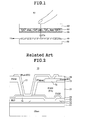
FIG. 1 illustrates an LCD device with a built-in touch screen according to the related art, and a method for driving the same. - Referring to
FIG. 1 , the LCD device with a built-in touch screen according to the related art comprises lower andupper substrates - On the
upper substrate 60, there are ablack matrix 62; red, green, andblue color filters overcoat layer 66. In this case, theblack matrix 62 defines a pixel region corresponding to each of plural pixels. Also, the red, green, andblue color filters black matrix 62. Theovercoat layer 66 covers the red, green, andblue color filters black matrix 62, to thereby planarize theupper substrate 60. - On the
lower substrate 50, there is apixel array 40 including plural pixels to drive the liquid crystal layer and detect a touching point by finger or pen. - Each of the plural pixels is defined by gate and data lines crossing each other. At the crossing portion of the gate and data lines, there is a thin film transistor (hereinafter, referred to as 'TFT'). Each of the plural pixels includes a common electrode and a pixel electrode.
- Recently, an in-cell touch type LCD device has been researched and developed, wherein the in-cell touch type LCD device refers to an LCD device that uses an element existing in the related art structure as a touch-sensing electrode (for example, a common electrode Vcom may be used as a touch-sensing electrode).
-
FIG. 2 is a cross section view illustrating a lower substrate in the LCD device with a built-in touch screen according to the related art.FIG. 2 shows a common electrode formed in the X-axis direction among all common electrodes of the LCD device. - In the LCD device with a built-in touch screen according to the related art, as shown in
FIG. 2 , acommon electrode 75 of alower substrate 50 not only supplies a common voltage (Vcom), but also functions as a sensing electrode for detection a user's touch. - For detection of the user's touch, the common electrodes (sensing electrode) 75 are formed in the X-axis and Y-axis directions. The
common electrode 75 in the X-axis direction is brought into contact with agate metal 73 at a lower portion of thelower substrate 50 through a contact structure, to be described. - In more detail, each pixel of the
lower substrate 50 includes abuffer layer 51 on a glass substrate; agate insulating layer 52; thegate metal 73; an interlayer dielectric (ILD) 53; acontact metal 74; a first passivation layer (PAS0) 54; a second passivation layer (PAS1) 55; the common electrode (Vcom) 75; a conductive line (3rd metal) 76; a third passivation layer (PAS2) 56; and acontact electrode 77. - The first to third passivation layers (PAS0 to PAS2) 54 to 56 are partially etched to thereby form a contact hole for exposing a predetermined portion of the
contact metal 74. - In addition, the third passivation layer (PAS2) 56 is additionally etched to expose the
conductive line 76. - The
gate metal 73 is formed of metal used for forming gate line. - The
contact metal 74 is formed of metal used for forming source and drain electrodes of TFT. - The
contact electrode 77 is formed of a transparent conductive material used for a pixel electrode (for example, ITO). Also, thecontact electrode 77 is formed simultaneously with the pixel electrode. - According as the first, second, and
third passivation layers contact metal 74 is formed in thecontact electrode 77. Also, theconductive line 76 is exposed by etching thethird passivation layer 56 thereabove. - The
contact electrode 77 is formed inside the contact hole and simultaneously on the third passivation layer (PAS2) 56. Thus, thecontact electrode 77 is electrically connected with thecontact metal 74 and theconductive line 76. - Through the contact structure between the
contact electrode 77 and thecontact metal 74, among the entire common electrodes driven as the touch-sensing electrode, thecommon electrode 75 in the X-axis direction is brought into contact with thegate metal 73. - For bringing the
common electrode 75 in the X-axis direction into contact with thegate metal 73 in the in-cell touch type LCD device according to the related art, thecontact electrode 77 is formed simultaneously with the pixel electrode. - If the
common electrode 75 is brought into contact with thegate metal 73 by the use of transparent metal for the pixel electrode, an aperture ratio of the corresponding pixel with the contact structure is relatively lower than that of the other pixels. - In order to connect the common electrodes of the neighboring pixels in the X-axis direction in the related art contact structure, the
conductive line 76 is connected with thecontact electrode 77, and thecontact metal 74 connected with thegate metal 73 is connected with thecontact electrode 77. This double contact structure may cause the structural problem of the increased size of the contact portion. - The aperture ratio in the pixel with the contact structure is lowered by the increased size of the contact portion. Especially, in case of the pixel structure with plural domains, the contact structure using the transparent metal of the pixel electrode is used so that an aperture ratio of the corresponding pixel is about 80% as compared to that of the neighboring pixels.
- Accordingly, the pixel with the contact structure may be shown as a dark point when a viewer watches the corresponding pixel with the contact structure, to thereby lower visibility. As a result, a picture quality of the LCD device is deteriorated. The double contact structure may cause the complicated manufacturing process and low manufacturing efficiency.
- Accordingly, the present invention is directed to an LCD device and a method for manufacturing the same that substantially obviates one or more problems due to limitations and disadvantages of the related art.
- An aspect of the present invention is to provide an LCD device and a method for manufacturing the same, which facilitates to realize high aperture ratio in a pixel with a contact structure between a gate metal and a conductive line for connection of a touch-sensing electrode (common electrode).
- Another aspect of the present invention is to provide an LCD device and a method for manufacturing the same, which facilitates to improve manufacturing efficiency owing to a simplified process of a lower substrate.
- Additional advantages and features of the invention will be set forth in part in the description which follows and in part will become apparent to those having ordinary skill in the art upon examination of the following or may be learned from practice of the invention. The objectives and other advantages of the invention may be realized and attained by the structure particularly pointed out in the written description and claims hereof as well as the appended drawings.
- To achieve these and other advantages and in accordance with the purpose of the invention, as embodied and broadly described herein, there is provided a liquid crystal display device with a built-in touch screen, which uses a common electrode as a touch-sensing electrode, comprising an intersection of a gate line and a data line to define a pixel region, a gate metal disposed in a central portion of the pixel, an insulating layer formed on the gate metal, a first contact hole disposed through the insulating layer to expose a predetermined portion of an upper surface of the gate metal, a contact metal on the insulating layer and inside the first contact hole, the contact metal electrically connected with the gate metal, a first passivation layer on the contact metal, a second contact hole disposed through the first passivation layer to expose a predetermined portion of an upper surface of the contact metal, a common electrode on the first passivation layer and inside the second contact hole, a conductive line electrically connected with the common electrode, and a second passivation layer on the first passivation layer and the conductive line, wherein the gate metal and the common electrode are electrically connected via the contact metal.
- In yet another aspect of the present invention, there is provided a method for manufacturing a liquid crystal display device with a built-in touch screen, which uses a common electrode as a touch-sensing electrode, comprising the steps of forming a pixel region defined by an intersection of a gate line and a data line, forming a gate metal disposed in a central portion of the pixel, forming an insulating layer on the gate metal, a first contact hole disposed through the insulating layer to expose a predetermined portion of an upper surface of the gate metal, forming a contact metal on the insulating layer and inside the first contact hole, the contact metal electrically connected with the gate metal, forming a first passivation layer on the contact metal, a second contact hole disposed through the first passivation layer to expose a predetermined portion of an upper surface of the contact metal, forming a common electrode on the first passivation layer and inside the second contact hole, forming a conductive line electrically connected with the common electrode, and forming a second passivation layer on the first passivation layer and the conductive line, wherein the gate metal and the common electrode are electrically connected via the contact metal.
- In yet another aspect of the present invention, there is provided a method for manufacturing an liquid crystal display device with a built-in touch screen comprising forming a first contact hole by etching a predetermined portion of an insulating layer on a gate metal, wherein the first contact hole exposes a predetermined portion of an upper surface of the gate metal, forming a contact metal on the insulating layer and inside the first contact hole, wherein the contact metal is electrically connected with the gate metal, forming a first passivation layer on the contact metal, and forming a second contact hole by etching a predetermined portion of the first passivation layer, wherein the second contact hole exposes a predetermined portion of an upper surface of the contact metal, forming a common electrode on the first passivation layer and inside the second contact hole, forming a conductive line inside the second contact hole, wherein the conductive line is electrically connected with the common electrode, and forming a second passivation layer on the first passivation layer and the conductive line, wherein the gate metal and the common electrode are electrically connected with each other via the contact metal.
- It is to be understood that both the foregoing general description and the following detailed description of the present invention are exemplary and explanatory and are intended to provide further explanation of the invention as claimed.
- The accompanying drawings, which are included to provide a further understanding of the invention and are incorporated in and constitute a part of this application, illustrate embodiment(s) of the invention and together with the description serve to explain the principle of the invention. In the drawings:
-
FIG. 1 illustrates an LCD device with a built-in touch screen according to the related art, and a method for manufacturing the same; -
FIG. 2 is a cross section view illustrating a lower substrate in an LCD device with a built-in touch screen according to the related art; -
FIGs. 3 and 4 illustrate an LCD device with a built-in touch screen according to the first embodiment of the present invention; -
FIGs. 5 and6 illustrate an LCD device with a built-in touch screen according to the second embodiment of the present invention; -
FIG. 7 illustrates an LCD device with a built-in touch screen according to the third embodiment of the present invention; and -
FIGs. 8A-8D illustrate a method for manufacturing an LCD device with a built-in touch screen according to the embodiment of the present invention. - Reference will now be made in detail to the exemplary embodiments of the present invention, examples of which are illustrated in the accompanying drawings. Wherever possible, the same reference numbers will be used throughout the drawings to refer to the same or like parts.
- Hereinafter, an LCD device with a built-in touch screen according to the present invention and a method for manufacturing the same will be described with reference to the accompanying drawings.
- For the following description of the embodiments of the present invention, if a first structure (for example, electrode, line, layer, contact, and etc.) is described as being formed "on" or "under" a second structure, the first and second structures may come in contact with each other, or there may be a third structure interposed between the first and second structures.
- Depending on an alignment mode of liquid crystal layer, an LCD device may be classified into Twisted-Nematic (TN) mode, Vertical-Alignment (VA) mode, In-Plane Switching (IPS) mode, and Fringe Field Switching (FFS) mode.
- In case of the IPS mode and the FFS mode, both a pixel electrode and a common electrode are formed on a lower substrate, whereby liquid crystal molecules of the liquid crystal layer are aligned depending on an electric field between the pixel electrode and the common electrode.
- Especially, in case of the IPS mode, the pixel electrode and the common electrode are alternately arranged in parallel so that an In-Plane mode electric field occurs between the pixel electrode and the common electrode, thereby aligning the liquid crystal molecules of the liquid crystal layer. However, in case of the IPS mode, the liquid crystal molecules are not properly aligned above the pixel electrode and the common electrode, whereby light transmittance is relatively deteriorated above the pixel electrode and the common electrode.
- In order to overcome this problem of the IPS mode, the FFS mode has been proposed. In case of the FFS mode, an insulating layer is interposed between the pixel electrode and the common electrode, whereby the pixel electrode is formed at a predetermined interval from the common electrode by the interposed insulating layer.
- In this case, any one of the pixel electrode and the common electrode is formed in a plate shape or pattern, and the other is formed in a finger shape, whereby a fringe field occurs between the pixel electrode and the common electrode. Thus, the liquid crystal molecules of the liquid crystal layer are aligned by the fringe field occurring between the pixel electrode and the common electrode.
- The LCD device with a built-in touch screen according to the embodiment of the present invention is formed in the FFS mode.
- The LCD device with a built-in touch screen according to the embodiment of the present invention comprises an in-cell touch type liquid crystal panel with a built-in touch screen for detection of a user's touch point; a backlight unit for supplying light to the liquid crystal panel; and a driving circuit.
- Herein, a contact structure between a gate metal and a common electrode driven as a touch-sensing electrode is a main point in this present invention. Thus, a detailed explanation for the driving circuit and the backlight unit will be omitted.
- For a display period, the LCD device with a built-in touch screen according to the embodiment of the present invention displays an image according to a video signal by controlling transmittance of light passing through a liquid crystal layer in each pixel.
- Meanwhile, for a non-display period, the common electrode on the lower substrate is driven as the touch-sensing electrode so as to sense the change of capacitance depending on a user's touch, and to detect the user's touch.
- On an upper substrate, there are a black matrix (BM); red, green, and blue color filters; and an overcoat layer.
- On a lower substrate, there is a pixel array including plural pixels to drive the liquid crystal layer and detect the touching point by sensing the capacitance depending on the user's touch.
- The pixel array includes gate and data lines crossing each other to defme the pixel; a common electrode; and a conductive line for connection of the common electrodes of the neighboring pixels. Also, a thin film transistor (TFT) serving as a switching element is formed in each pixel, and is connected with a pixel electrode.
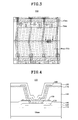
-
FIGs. 3 and 4 illustrate an LCD device with a built-in touch screen according to the first embodiment of the present invention.FIG. 4 is a cross section view along I-I' ofFIG. 3 . -
FIGs. 3 and 4 show a contact portion between a gate metal and a common electrode in an entire pixel region of a lower substrate. - In the LCD with a built-in touch screen according to the first embodiment of the present invention, the contact structure between the gate metal and the common electrode has an overlap portion, to thereby realize high aperture ratio in the corresponding pixel with the contact structure of common electrode.
- Referring to
FIGs. 3 and 4 , on thelower substrate 100, there are abuffer layer 110; a gate insulating layer (GI) 120; agate metal 130; an interlayer dielectric (ILD) 140; acontact metal 150; a first passivation layer (PAS1) 160; a common electrode (Vcom) 170; aconductive line 180; and a second passivation layer (PAS2) 190. - The
buffer layer 110 and thegate insulating layer 120 are sequentially formed on a glass substrate. Then, thegate metal 130 is formed on thegate insulating layer 120. Thegate metal 130 is formed of metal used for forming the gate line, wherein thegate metal 130 is positioned in the central portion of the pixel. - Although not shown, an active layer (semiconductor layer) is formed below the
gate insulating layer 120 of a TFT region. Also, a channel of the TFT is formed in an overlap region between the active layer and a gate electrode diverged from the gate line. - Then, TEOS (Tetra Ethyl Ortho Silicate) or MTO (Middle Temperature Oxide) may be deposited to cover the
gate metal 130 by CVD (Chemical Vapor Deposition), thereby forming theinterlayer dielectric 140. - A predetermined portion of an upper surface of the
gate metal 130 is exposed by etching a predetermined portion of theinterlayer dielectric 140. Also, predetermined portions of thecontact metal 150, positioned on theinterlayer dielectric 140, are overlapped with thegate metal 130. - In the exposed portion of the
gate metal 130, thecontact metal 150 is electrically connected with thegate metal 130. - At this time, the
contact metal 150 is brought into contact with the central portion of thegate metal 130. That is, thegate metal 130 is overlapped with thecontact metal 150. - The
contact metal 150 may be formed of metal used for formation of source and drain electrodes of the TFT. Also, thecontact metal 150 may be formed simultaneously with the source and drain electrodes of the TFT. - The first passivation layer (PAS 1) 160 is formed on the
interlayer dielectric 140 and thecontact metal 150. A predetermined portion of an upper surface of thecontact metal 150 is exposed by partially etching the first passivation layer (PAS1) 160 above the contact portion between thegate metal 130 and thecontact metal 150. - The
common electrode 170 is formed of a transparent conductive material such as ITO. Thecommon electrode 170 is formed on the first passivation layer (PAS 1) 160, and simultaneously formed inside the contact hole obtained by partially etching the first passivation layer (PAS1) 160. Inside the contact hole, thecontact metal 150 is electrically connected with thecommon electrode 170. - For a display period of one frame or plural frames, the
common electrode 170 supplies the common voltage for controlling the transmittance of light passing through the liquid crystal layer to the pixel. - For a non-display period of one frame or plural frames, the
common electrode 170 is driven as the touch-sensing electrode to detect the change of capacitance (Ctc) depending on the user's touch. - Generally, the common electrode of the LCD device according to the related art is formed in a plate shape to supply the same common voltage (Vcom) to the entire pixel region of the lower substrate.
- The
common electrode 170 of the LCD device according to the first embodiment of the present invention not only supplies the common voltage (Vcom), but also functions as the touch-sensing electrode for detection the user's touch. - Accordingly, the
common electrode 170 is patterned every individual pixel. Thecommon electrode 170 may be patterned every predetermined number of the pixels. - The common electrodes of the neighboring pixels may be connected via the
conductive line 180 by the X-axis direction or Y-axis direction. At this time, the common electrodes of the X-axis direction are brought into contact with thegate metal 130 through the aforementioned contact structure. - The
conductive line 180 is formed by depositing (burying) a metal material on the first passivation layer (PAS 1) 160 and inside the contact hole obtained by etching the first passivation layer (PAS1) 160. Theconductive line 180 is brought into contact with thecommon electrode 170. - At this time, the
conductive line 180 may be formed as the contact line to make thecommon electrode 170 driven as the touch-sensing electrode for detection of the user's touch. - The second passivation layer (PAS2) 190 is formed to cover the
common electrode 170 and theconductive line 180. - The above LCD device with a built-in touch screen according to the first embodiment of the present invention has the contact structure where the
gate metal 130, thecontact metal 150, thecommon electrode 170, and theconductive line 180 are overlapped with one another in the same vertical line. - For the contact between the common electrode and the gate metal, in case of the related art of
FIG. 2 , the conductive line is firstly brought into contact with the pixel electrode by the use of pixel electrode, and then the pixel electrode is secondly brought into contact with the contact electrode, to thereby make the double contact structure. Owing to the double contact structure, the aperture ratio may be lowered in the corresponding pixel with the contact structure. - However, in case of the LCD device with a built-in touch screen according to the first embodiment of the present invention, the
gate metal 130 is directly brought into contact with thecommon electrode 170 while being overlapped with thecommon electrode 170 in the same vertical line, to thereby realize the high aperture ratio. - Especially, as shown in
FIG. 3 , the above contact structure is formed in the central portion of disclination in the multi-domain pixel structure, whereby the aperture ratio of the corresponding pixel is increased to be about 90% as compared to that of the neighboring pixels (wherein, the neighboring pixel indicates the pixel without the contact structure). -
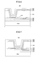
FIGs. 5 and6 illustrate an LCD device with a built-in touch screen according to the second embodiment of the present invention.FIG. 6 is a cross section view along II-II' ofFIG. 5 . -
FIGs. 5 and6 show a contact portion between a gate metal and a common electrode in an entire pixel region of a lower substrate. - Except for an overlap shape of a contact structure, and an element for reducing step coverage of overlap, the LCD device according to the second embodiment of the present invention is identical in structure to the LCD device according to the first embodiment of the present invention.
- Thus, wherever possible, the same reference numbers will be used throughout the drawings to refer to the same or like parts, except parts of the contact structure. Also, a detailed explanation for the same parts as those of the first embodiment will be omitted.
- In the LCD device with a built-in touch screen according to the second embodiment of the present invention, a contact structure between a gate metal and a common electrode has an overlap portion, thereby increasing aperture ratio of the pixel with the contact structure, and reducing step coverage by the overlap portion of the contact structure.
- Referring to
FIGs. 5 and6 , on alower substrate 200, there are abuffer layer 110; a gate insulating layer (GI) 120; agate metal 130; an interlayer dielectric (ILD) 240; acontact metal 250; a first passivation layer (PAS1) 260; a common electrode (Vcom) 270; a conductive line (3rd metal) 280; and a second passivation layer (PAS2) 290. - The interlayer dielectric (ILD) 240 is formed to cover the
gate metal 130. A predetermined portion of an upper surface of thegate metal 130 is exposed by partially etching a predetermined portion of theinterlayer dielectric 240. - The
contact metal 250 is overlapped with thegate metal 130 above theinterlayer dielectric 240. In the exposed portion of thegate metal 130, thecontact metal 250 is electrically connected with thegate metal 130. At this time, the contact portion between thegate metal 130 and thecontact metal 250 is provided at one side with respect to the central portion of thegate metal 130. - At this time, the
contact metal 250 may be formed of metal used for formation of source and drain electrodes of the TFT. Also, thecontact metal 250 may be formed simultaneously with the source and drain electrodes of the TFT. - The
gate metal 130 is overlapped with thecontact metal 250. - The first passivation layer (PAS 1) 260 is formed on the
interlayer dielectric 240 and thecontact metal 250. - A contact hole is formed by etching a predetermined portion of the
first passivation layer 260. Via this contact hole, a predetermined portion of an upper surface of thecontact metal 250 is exposed. In this case, the predetermined portion of thefirst passivation layer 260, which is not overlapped with the contact portion between thegate metal 130 and thecontact metal 250, is etched. - The
common electrode 270 is formed on the first passivation layer (PAS1) 260, and is also formed inside the contact hole realized by etching the first passivation layer (PAS1) 260. Inside the contact hole, thecontact metal 250 is electrically connected with thecommon electrode 270. - The common electrodes of the neighboring pixels may be connected via the
conductive line 280 by the X-axis direction or Y-axis direction. At this time, the common electrodes of the X-axis direction are brought into contact with thegate metal 130 through the aforementioned contact structure. - The
conductive line 280 is formed by depositing (burying) a metal material on the first passivation layer (PAS1) 260 and inside the contact hole obtained by etching the first passivation layer (PAS1) 260. Theconductive line 280 is brought into contact with thecommon electrode 270. - At this time, the
conductive line 280 may be formed as the contact line to make thecommon electrode 270 driven as the touch-sensing electrode for detection of the user's touch. - The second passivation layer (PAS2) 290 is formed to cover the
common electrode 270 and theconductive line 280. - In case of the LCD device according to the first embodiment of the present invention, the gate metal and the common electrode are brought into contact with each other via the contact metal, wherein the gate metal, the common electrode, and the contact metal are overlapped in the same vertical line.
- In case of the LCD device according to the second embodiment of the present invention, the contact portion between the
gate metal 130 and thecontact metal 250, and the contact portion between thecontact metal 250 and thecommon electrode 270 are provided at the different vertical lines. - Thus, the aperture ratio of the pixel may be increased owing to the contact between the
gate metal 130 and thecommon electrode 270 via thecontact metal 250. Also, it is possible to reduce the step coverage caused by the contact structure. - In case of the LCD device with a built-in touch screen according to the second embodiment of the present invention, as shown in
FIG. 5 , the contact structure is formed in the central portion of disclination in the multi-domain pixel structure, thereby realizing the high aperture ratio in the corresponding pixel. -
FIG. 7 illustrates an LCD device with a built-in touch screen according to the third embodiment of the present invention.FIG. 7 shows a contact portion between a gate metal and a common electrode in an entire pixel region of a lower substrate. - Except for an overlap shape of a contact structure, and an element for reducing step coverage of overlap, the LCD device according to the third embodiment of the present invention is identical in structure to the LCD device according to the first embodiment of the present invention.
- Thus, wherever possible, the same reference numbers will be used throughout the drawings to refer to the same or like parts, except parts of the contact structure. Also, a detailed explanation for the same parts as those of the first embodiment will be omitted.
- In the LCD device with a built-in touch screen according to the third embodiment of the present invention, a contact structure between a gate metal and a common electrode has an overlap portion, thereby increasing aperture ratio of the pixel with the contact structure, and reducing step coverage by the overlap portion of the contact structure.
- Referring to
FIG. 7 , on alower substrate 300, there are abuffer layer 110; a gate insulating layer (GI) 120; agate metal 130; an interlayer dielectric (ILD) 340; acontact metal 350; a first passivation layer (PAS1) 360; a common electrode (Vcom) 370; aconductive line 380; and a second passivation layer (PAS2) 390. - The interlayer dielectric (ILD) 340 is formed to cover the
gate metal 130. A predetermined portion of an upper surface of thegate metal 130 is exposed by partially etching a predetermined portion of theinterlayer dielectric 340. - The
contact metal 350 is overlapped with thegate metal 130 above theinterlayer dielectric 340. In the exposed portion of thegate metal 130, thecontact metal 350 is electrically connected with thegate metal 130. At this time, the contact portion between thegate metal 130 and thecontact metal 350 is positioned at one side with respect to the central portion of thegate metal 130. - At this time, the
contact metal 350 may be formed of metal used for formation of source and drain electrodes of the TFT. Thegate metal 130 is overlapped with thecontact metal 350. - The first passivation layer (PAS1) 360 is formed on the
interlayer dielectric 340 and thecontact metal 350. A contact hole is formed by etching a predetermined portion of thefirst passivation layer 360. A predetermined portion of an upper surface of thecontact metal 350 is exposed through the contact hole. At this time, the etched portion of the first passivation layer (PAS1) 360 is partially overlapped with the contact portion between thegate metal 130 and thecontact metal 350. - The
common electrode 370 is formed on the first passivation layer (PAS1) 360, and is formed inside the contact hole obtained by etching the first passivation layer (PAS1) 360. Inside the contact hole, thecontact metal 350 is electrically connected with thecommon electrode 370. - The
common electrodes 370 of the neighboring pixels are connected via theconductive line 370 by the X-axis direction or Y-axis direction. Thecommon electrodes 370 of the X-axis direction are brought into contact with thegate metal 130 through the above contact structure. - The
conductive line 380 is formed by depositing (burying) a metal material on the first passivation layer (PAS1) 360 and inside the contact hole obtained by etching the first passivation layer (PAS1) 360. Theconductive line 380 is brought into contact with thecommon electrode 370. - At this time, the
conductive line 380 may be formed as the contact line to make thecommon electrode 370 driven as the touch-sensing electrode for detection of the user's touch. - The second passivation layer (PAS2) 390 is formed to cover the
common electrode 370 and theconductive line 380. - The above LCD device with a built-in touch screen according to the first embodiment of the present invention has the contact structure where the gate metal and the common electrode are overlapped with each other in the same vertical line.
- Meanwhile, the LCD device with a built-in touch screen according to the third embodiment of the present invention has the contact structure where the contact portion between the
gate metal 130 and thecontact metal 350 is partially overlapped with the contact portion between thecontact metal 350 and thecommon electrode 370 in the vertical line. - Thus, the aperture ratio of the pixel may be increased owing to the contact between the
gate metal 130 and thecommon electrode 370 through thecontact metal 350. Also, it is possible to reduce the step coverage caused by the contact structure. - In case of the LCD device with a built-in touch screen according to the third embodiment of the present invention, the contact structure is formed in the central portion of disclination in the multi-domain pixel structure, thereby realizing the high aperture ratio in the corresponding pixel.
- The LCD devices according to the first to third embodiments of the present invention provides the good visibility of the pixel and good display quality by improving the contact structure between the gate metal and the common electrode.
- Hereinafter, a method for manufacturing the LCD device with a built-in touch screen according to the embodiment of the present invention will be described with reference to
FIG. 8 . -
FIG. 8 illustrates a method for manufacturing the LCD device according to the first embodiment of the present invention. - As shown in
FIG. 8A , thebuffer layer 110 is formed on the substrate. Then, TEOS (Tetra Ethyl Ortho Silicate) or MTO (Middle Temperature Oxide) may be deposited on an entire surface of the substrate, to thereby form thegate insulating layer 120. - Thereafter, a metal material is deposited on the
gate insulating layer 120, and then photolithography and dry-etching process using a mask is applied to the deposited metal material, to thereby form thegate metal 130. - The substrate may be formed of glass or plastic material.
FIGs. 8A-8D show the exemplary case using the glass substrate. - As shown in
FIG. 8B , an insulating material is deposited on the substrate to cover thegate metal 130 and thegate insulating layer 120, thereby forming the interlayer dielectric (ILD) 140. - Then, photolithography and dry-etching process using a mask is carried out to etch a predetermined portion of the
interlayer dielectric 140, thereby forming the first contact hole for exposing the upper surface of the central portion of thegate metal 130. - Then, a metal material is deposited to cover the
interlayer dielectric 140, and photolithography and wet-etching process using a mask is applied to the deposited metal material, to thereby form thecontact metal 150. - The
contact metal 150 is formed by the process for forming the source and drain electrodes of the TFT, and is simultaneously with the source and drain electrodes of the TFT. Thegate metal 130 and thecontact metal 150 are electrically connected with each other inside the first contact hole obtained by etching theinterlayer dielectric 140. - As shown in
FIG. 8C , the first passivation layer (PAS1) 160 is formed to cover theinterlayer dielectric 140 and thecontact metal 150, and then photolithography and etching process is applied thereto, to thereby form the second contact hole. - The second contact hole is formed in the contact portion between the
gate metal 130 and thecontact metal 150. - After that, a transparent conductive material such as ITO is deposited on the first passivation layer (PAS 1) 160, and is formed inside the second contact hole, to thereby form the common electrode (Vcom) 170. Thus, the
gate metal 130 and thecommon electrode 170 are electrically connected with each other via thecontact metal 150 inside the second contact hole. - As shown in
FIG. 8D , a conductive metal material is deposited on thecommon electrode 170, and photolithography and etching process using a mask is applied to the deposited conductive metal material, to thereby form theconductive line 180 electrically connected with thecommon electrode 170. - The second passivation layer (PAS2) 190 is formed to cover the
common electrode 170 and theconductive line 180. - In the method for manufacturing the LCD device with a built-in touch screen according to the embodiment of the present invention, the gate metal and the common electrode are overlapped in the same vertical line, to thereby realize the high aperture ratio in the pixel with the contact structure.
- Also, the passivation layer PAS0, which has been applied to the related art structure, is omitted so that the contact structure and the manufacturing process are simplified, thereby improving the manufacturing efficiency and price competition of the LCD device with a built-in touch screen according to the present invention.
- Although not shown, the method for manufacturing the LCD device with a built-in touch screen according to another embodiment of the present invention, the first contact hole and the second contact hole, which are formed by the processes of
FIG. 8B and FIG. 8C , are not overlapped with each other, to thereby form the contact structure according to the second embodiment of the present invention, as shown inFIG. 6 . - The contact structure according to the third embodiment of the present invention may be obtained by partially overlapping the first and second contact holes, as shown in
FIG. 7 . - The LCD device according to an embodiment of the present invention has the contact structure where the touch-sensing electrode (common electrode) is brought into contact with the gate metal, to thereby improve the display quality owing to the high aperture ratio of the pixel.
- In case of the LCD device according to the second embodiment of the present invention, the contact structure between the common electrode and the gate metal is formed in the central portion of disclination in the multi-domain pixel structure, thereby realizing the high aperture ratio in the corresponding pixel.
- Also, the simplified manufacturing process of the lower substrate in the LCD device according to the present invention enables to reduce the manufacturing cost of the LCD device, and to improve the manufacturing efficiency.
- It will be apparent to those skilled in the art that various modifications and variations can be made in the present invention without departing from the spirit or scope of the inventions. Thus, it is intended that the present invention covers the modifications and variations of this invention provided they come within the scope of the appended claims and their equivalents.
Claims (15)
- A liquid crystal display device with a built-in touch screen, which uses a common electrode as a touch-sensing electrode, comprising:an intersection of a gate line and a data line to define a pixel region;a gate metal disposed in a central portion of the pixel;an insulating layer formed on the gate metal, a first contact hole disposed through the insulating layer to expose a predetermined portion of an upper surface of the gate metal;a contact metal on the insulating layer and inside the first contact hole, the contact metal electrically connected with the gate metal;a first passivation layer on the contact metal, a second contact hole disposed through the first passivation layer to expose a predetermined portion of an upper surface of the contact metal;a common electrode on the first passivation layer and inside the second contact hole; a conductive line electrically connected with the common electrode; anda second passivation layer on the first passivation layer and the conductive line,wherein the gate metal and the common electrode are electrically connected via the contact metal.
- The liquid crystal display device according to claim 1, wherein a first contact portion between the gate metal and the contact metal is at least partially overlapped with a second contact portion between the contact metal and the common electrode.
- The liquid crystal display device according to claim 2, wherein the first and second contact portions are overlapped with the central portion of the gate metal.
- The liquid crystal display device according to claim 2, wherein the first contact portion is overlapped with one side of the gate metal, and the second contact portion is overlapped with the other side of the gate metal.
- The liquid crystal display device according to claim 1, wherein the first contact portion between the gate metal and the contact metal is not overlapped with the second contact portion between the contact metal and the common electrode.
- The liquid crystal display device according to claim 1, wherein the first contact portion between the gate metal and the contact metal, and the second contact portion between the contact metal and the common electrode are formed in the central portion of disclination of multi-domain.
- The liquid crystal display device according to claim 6, wherein an aperture ratio in the pixels with the first contact portion and the second contact portion is about 90% or more as compared to that of the neighboring pixels.
- The liquid crystal display device according to claim 1, wherein the common electrodes of the neighboring pixels in the X-axis direction are connected through the gate metal.
- A method for manufacturing a liquid crystal display device with a built-in touch screen, which uses a common electrode as a touch-sensing electrode, comprising the steps of:forming a pixel region defined by an intersection of a gate line and a data line;forming a gate metal disposed in a central portion of the pixel;forming an insulating layer on the gate metal, a first contact hole disposed through the insulating layer to expose a predetermined portion of an upper surface of the gate metal;forming a contact metal on the insulating layer and inside the first contact hole, the contact metal electrically connected with the gate metal;forming a first passivation layer on the contact metal, a second contact hole disposed through the first passivation layer to expose a predetermined portion of an upper surface of the contact metal;forming a common electrode on the first passivation layer and inside the second contact hole;forming a conductive line electrically connected with the common electrode; andforming a second passivation layer on the first passivation layer and the conductive line,wherein the gate metal and the common electrode are electrically connected via the contact metal.
- The method according to claim 9, wherein a first contact portion between the gate metal and the contact metal at least partially overlaps a second contact portion between the contact metal and the common electrode, wherein the first and second contact holes are partially overlapped with each other.
- The method according to claim 9, wherein a first and second contact portions overlap the central portion of the gate metal, wherein the first contact hole is formed corresponding to the central portion of the gate metal, and the second contact hole is formed while being overlapped with the first contact hole.
- The method according to claim 11, wherein the first contact portion overlaps one side of the gate metal, and the second contact portion overlaps the other side of the gate metal, wherein the first contact hole is formed at one side with respect to the central portion of the gate metal, and the second contact hole is formed at the other side with respect to the central portion of the gate metal.
- The method according to claim 9, wherein a first contact portion between the gate metal and the contact metal does not overlap a second contact portion between the contact metal and the common electrode, wherein the first and second contact holes are not overlapped with each other.
- The method according to claim 9, wherein a first contact portion between the gate metal and the contact metal, and a second contact portion between the contact metal and the common electrode are formed in the central portion of disclination of a multi-domain structure.
- The method according to claim 9, wherein the first contact hole is formed by etching a predetermined portion of the insulating layer corresponding to the gate metal, and the second contact hole is formed by etching a predetermined portion of the first passivation layer corresponding to the contact metal.
Applications Claiming Priority (1)
| Application Number | Priority Date | Filing Date | Title |
|---|---|---|---|
| KR1020100092392A KR101284714B1 (en) | 2010-09-20 | 2010-09-20 | Liquid crystal display device and method for manufacturing the same |
Publications (2)
| Publication Number | Publication Date |
|---|---|
| EP2431802A1 true EP2431802A1 (en) | 2012-03-21 |
| EP2431802B1 EP2431802B1 (en) | 2017-12-06 |
Family
ID=44650885
Family Applications (1)
| Application Number | Title | Priority Date | Filing Date |
|---|---|---|---|
| EP11007618.9A Active EP2431802B1 (en) | 2010-09-20 | 2011-09-19 | Liquid crystal display device and method for manufacturing the same |
Country Status (5)
| Country | Link |
|---|---|
| US (1) | US8792060B2 (en) |
| EP (1) | EP2431802B1 (en) |
| KR (1) | KR101284714B1 (en) |
| CN (1) | CN102411238B (en) |
| TW (1) | TWI448776B (en) |
Cited By (1)
| Publication number | Priority date | Publication date | Assignee | Title |
|---|---|---|---|---|
| CN106200077A (en) * | 2016-08-31 | 2016-12-07 | 深圳市华星光电技术有限公司 | A kind of contact panel and preparation method thereof |
Families Citing this family (17)
| Publication number | Priority date | Publication date | Assignee | Title |
|---|---|---|---|---|
| US9720295B2 (en) * | 2011-09-27 | 2017-08-01 | Lg Display Co., Ltd. | Liquid crystal display device and method for manufacturing the same |
| CN103135815B (en) * | 2011-11-25 | 2017-02-22 | 上海天马微电子有限公司 | Embedded touch screen liquid crystal display device and touch control driving method thereof |
| JP2015187754A (en) * | 2012-08-09 | 2015-10-29 | シャープ株式会社 | liquid crystal display device |
| KR102017204B1 (en) | 2012-11-01 | 2019-09-03 | 삼성디스플레이 주식회사 | Thin film trannsistor array panel and manufacturing method thereof |
| US9560738B2 (en) * | 2012-11-22 | 2017-01-31 | Lg Innotek Co., Ltd. | Touch window |
| JP6253923B2 (en) * | 2013-08-30 | 2017-12-27 | 株式会社ジャパンディスプレイ | Organic electroluminescence device with built-in touch sensor |
| US9543335B2 (en) | 2014-07-17 | 2017-01-10 | Innolux Corporation | Liquid-crystal display and element substrate thereof |
| TWI567452B (en) * | 2014-07-17 | 2017-01-21 | 群創光電股份有限公司 | Liquid crystal display and element substrate thereof |
| CN104461142B (en) * | 2014-12-10 | 2017-06-30 | 京东方科技集团股份有限公司 | Touch display substrate and preparation method thereof, touch control display apparatus |
| KR101727108B1 (en) * | 2014-12-31 | 2017-04-17 | 엘지디스플레이 주식회사 | In cell touch liquid crystal display device and method for manufacturing the same |
| CN104503647B (en) * | 2014-12-31 | 2017-12-08 | 京东方科技集团股份有限公司 | Substrate and its manufacture method, the touch-screen and display device of a kind of touch display screen |
| CN104698665B (en) | 2015-04-01 | 2017-11-07 | 上海天马微电子有限公司 | Touch display panel structure and forming method thereof, touch control display apparatus |
| CN106873267B (en) * | 2015-12-14 | 2021-02-19 | 群创光电股份有限公司 | Display panel |
| CN106896609B (en) * | 2017-04-28 | 2019-11-19 | 厦门天马微电子有限公司 | A kind of array substrate and the display device including it |
| CN107402671B (en) * | 2017-06-19 | 2020-03-17 | 南京中电熊猫液晶显示科技有限公司 | Embedded touch panel and manufacturing method thereof |
| CN113728299B (en) * | 2020-03-24 | 2023-05-16 | 京东方科技集团股份有限公司 | Array substrate and display device |
| KR20230011079A (en) | 2021-07-13 | 2023-01-20 | (주)에이케이테크 | Stator for motor made of synthetic resin and wire for using thereof |
Citations (3)
| Publication number | Priority date | Publication date | Assignee | Title |
|---|---|---|---|---|
| WO2010084642A1 (en) * | 2009-01-26 | 2010-07-29 | シャープ株式会社 | Touch panel incorporated into display device |
| EP2214084A1 (en) * | 2009-02-02 | 2010-08-04 | Apple Inc. | Integrated touch screen |
| KR20100092392A (en) | 2009-02-12 | 2010-08-20 | 제록스 코포레이션 | Organoamine stabilized silver nanoparticles and process for producing same |
Family Cites Families (8)
| Publication number | Priority date | Publication date | Assignee | Title |
|---|---|---|---|---|
| KR101211345B1 (en) | 2005-12-14 | 2012-12-11 | 엘지디스플레이 주식회사 | Liquid Crystal Display Device And Method For Fabricating Thereof |
| CN100426511C (en) * | 2006-06-23 | 2008-10-15 | 北京京东方光电科技有限公司 | Baseplate structure of thin film transistor device array, and preparation method |
| KR20080052836A (en) * | 2006-12-08 | 2008-06-12 | 삼성전자주식회사 | Liquid crystal display device and method for manufacturing the same |
| WO2008108042A1 (en) | 2007-03-01 | 2008-09-12 | Sharp Kabushiki Kaisha | Display panel substrate, display panel, display device and method for manufacturing display panel substrate |
| JP5207163B2 (en) * | 2007-03-30 | 2013-06-12 | Nltテクノロジー株式会社 | Method for forming embedded wiring, display device substrate, and display device having the substrate |
| TWI384277B (en) * | 2007-09-07 | 2013-02-01 | Japan Display West Inc | Liquid crystal display apparatus |
| KR101564332B1 (en) * | 2008-10-28 | 2015-10-30 | 삼성전자주식회사 | Touch screen panel integrated with liquid crystal display method of manufacturing the same and method of touch sensing |
| JP5140018B2 (en) | 2009-02-24 | 2013-02-06 | 株式会社ジャパンディスプレイイースト | LCD with input function |
-
2010
- 2010-09-20 KR KR1020100092392A patent/KR101284714B1/en active IP Right Grant
-
2011
- 2011-08-04 US US13/198,175 patent/US8792060B2/en active Active
- 2011-08-09 TW TW100128396A patent/TWI448776B/en active
- 2011-09-02 CN CN201110263524.6A patent/CN102411238B/en active Active
- 2011-09-19 EP EP11007618.9A patent/EP2431802B1/en active Active
Patent Citations (3)
| Publication number | Priority date | Publication date | Assignee | Title |
|---|---|---|---|---|
| WO2010084642A1 (en) * | 2009-01-26 | 2010-07-29 | シャープ株式会社 | Touch panel incorporated into display device |
| EP2214084A1 (en) * | 2009-02-02 | 2010-08-04 | Apple Inc. | Integrated touch screen |
| KR20100092392A (en) | 2009-02-12 | 2010-08-20 | 제록스 코포레이션 | Organoamine stabilized silver nanoparticles and process for producing same |
Cited By (1)
| Publication number | Priority date | Publication date | Assignee | Title |
|---|---|---|---|---|
| CN106200077A (en) * | 2016-08-31 | 2016-12-07 | 深圳市华星光电技术有限公司 | A kind of contact panel and preparation method thereof |
Also Published As
| Publication number | Publication date |
|---|---|
| US8792060B2 (en) | 2014-07-29 |
| US20120068200A1 (en) | 2012-03-22 |
| EP2431802B1 (en) | 2017-12-06 |
| CN102411238B (en) | 2014-10-29 |
| TW201213944A (en) | 2012-04-01 |
| TWI448776B (en) | 2014-08-11 |
| KR20120030709A (en) | 2012-03-29 |
| CN102411238A (en) | 2012-04-11 |
| KR101284714B1 (en) | 2013-07-17 |
Similar Documents
| Publication | Publication Date | Title |
|---|---|---|
| EP2431802B1 (en) | Liquid crystal display device and method for manufacturing the same | |
| EP2431847B1 (en) | Liquid crystal display device with a built-in touch screen and method for manufacturing the same | |
| US9218082B2 (en) | Liquid crystal display device with a built-in touch screen and method for manufacturing the same | |
| US10310345B2 (en) | In-cell touch liquid crystal display apparatus, method of manufacturing the same, method of manufacturing thin film transistor array substrate, and method of manufacturing color filter array substrate | |
| US9971181B2 (en) | In-cell touch liquid crystal display device and method for manufacturing the same | |
| US8698971B2 (en) | Liquid crystal display device and method for manufacturing the same | |
| US9036105B2 (en) | Liquid crystal display device and method of manufacturing the same | |
| US8878814B2 (en) | Liquid crystal display device provided with a sensing electrode for sensing a touch of a user | |
| US8982064B2 (en) | Liquid crystal display device provided with a sensing electrode for sending a touch of a user | |
| US8743301B2 (en) | Liquid crystal display device provided with an electrode for sensing a touch of a user | |
| US9568760B2 (en) | In-cell touch liquid crystal display apparatus and method of manufacturing the same | |
| US8792061B2 (en) | Liquid crystal display device | |
| US20150116622A1 (en) | Liquid crystal display device and method of manufacturing the same | |
| US20120050660A1 (en) | Liquid Crystal Display Device | |
| KR20130035684A (en) | Liquid crystal display apparatus and method for manufacturing the same | |
| KR101810503B1 (en) | Liquid crystal display device with a built in touch screen | |
| KR20160082810A (en) | In Cell Touch Liquid Crystal Display Device | |
| KR101705557B1 (en) | Liquid crystal display device with a built in touch screen |
Legal Events
| Date | Code | Title | Description |
|---|---|---|---|
| PUAI | Public reference made under article 153(3) epc to a published international application that has entered the european phase |
Free format text: ORIGINAL CODE: 0009012 |
|
| AK | Designated contracting states |
Kind code of ref document: A1 Designated state(s): AL AT BE BG CH CY CZ DE DK EE ES FI FR GB GR HR HU IE IS IT LI LT LU LV MC MK MT NL NO PL PT RO RS SE SI SK SM TR |
|
| AX | Request for extension of the european patent |
Extension state: BA ME |
|
| 17P | Request for examination filed |
Effective date: 20120914 |
|
| 17Q | First examination report despatched |
Effective date: 20150225 |
|
| GRAP | Despatch of communication of intention to grant a patent |
Free format text: ORIGINAL CODE: EPIDOSNIGR1 |
|
| GRAJ | Information related to disapproval of communication of intention to grant by the applicant or resumption of examination proceedings by the epo deleted |
Free format text: ORIGINAL CODE: EPIDOSDIGR1 |
|
| GRAP | Despatch of communication of intention to grant a patent |
Free format text: ORIGINAL CODE: EPIDOSNIGR1 |
|
| INTG | Intention to grant announced |
Effective date: 20170703 |
|
| INTG | Intention to grant announced |
Effective date: 20170713 |
|
| RAP1 | Party data changed (applicant data changed or rights of an application transferred) |
Owner name: LG DISPLAY CO., LTD. |
|
| GRAS | Grant fee paid |
Free format text: ORIGINAL CODE: EPIDOSNIGR3 |
|
| GRAA | (expected) grant |
Free format text: ORIGINAL CODE: 0009210 |
|
| AK | Designated contracting states |
Kind code of ref document: B1 Designated state(s): AL AT BE BG CH CY CZ DE DK EE ES FI FR GB GR HR HU IE IS IT LI LT LU LV MC MK MT NL NO PL PT RO RS SE SI SK SM TR |
|
| REG | Reference to a national code |
Ref country code: GB Ref legal event code: FG4D |
|
| REG | Reference to a national code |
Ref country code: AT Ref legal event code: REF Ref document number: 952893 Country of ref document: AT Kind code of ref document: T Effective date: 20171215 Ref country code: CH Ref legal event code: EP |
|
| REG | Reference to a national code |
Ref country code: IE Ref legal event code: FG4D |
|
| REG | Reference to a national code |
Ref country code: DE Ref legal event code: R096 Ref document number: 602011043898 Country of ref document: DE |
|
| REG | Reference to a national code |
Ref country code: NL Ref legal event code: MP Effective date: 20171206 |
|
| REG | Reference to a national code |
Ref country code: LT Ref legal event code: MG4D |
|
| PG25 | Lapsed in a contracting state [announced via postgrant information from national office to epo] |
Ref country code: SE Free format text: LAPSE BECAUSE OF FAILURE TO SUBMIT A TRANSLATION OF THE DESCRIPTION OR TO PAY THE FEE WITHIN THE PRESCRIBED TIME-LIMIT Effective date: 20171206 Ref country code: LT Free format text: LAPSE BECAUSE OF FAILURE TO SUBMIT A TRANSLATION OF THE DESCRIPTION OR TO PAY THE FEE WITHIN THE PRESCRIBED TIME-LIMIT Effective date: 20171206 Ref country code: NO Free format text: LAPSE BECAUSE OF FAILURE TO SUBMIT A TRANSLATION OF THE DESCRIPTION OR TO PAY THE FEE WITHIN THE PRESCRIBED TIME-LIMIT Effective date: 20180306 Ref country code: ES Free format text: LAPSE BECAUSE OF FAILURE TO SUBMIT A TRANSLATION OF THE DESCRIPTION OR TO PAY THE FEE WITHIN THE PRESCRIBED TIME-LIMIT Effective date: 20171206 Ref country code: FI Free format text: LAPSE BECAUSE OF FAILURE TO SUBMIT A TRANSLATION OF THE DESCRIPTION OR TO PAY THE FEE WITHIN THE PRESCRIBED TIME-LIMIT Effective date: 20171206 |
|
| REG | Reference to a national code |
Ref country code: AT Ref legal event code: MK05 Ref document number: 952893 Country of ref document: AT Kind code of ref document: T Effective date: 20171206 |
|
| PG25 | Lapsed in a contracting state [announced via postgrant information from national office to epo] |
Ref country code: GR Free format text: LAPSE BECAUSE OF FAILURE TO SUBMIT A TRANSLATION OF THE DESCRIPTION OR TO PAY THE FEE WITHIN THE PRESCRIBED TIME-LIMIT Effective date: 20180307 Ref country code: RS Free format text: LAPSE BECAUSE OF FAILURE TO SUBMIT A TRANSLATION OF THE DESCRIPTION OR TO PAY THE FEE WITHIN THE PRESCRIBED TIME-LIMIT Effective date: 20171206 Ref country code: HR Free format text: LAPSE BECAUSE OF FAILURE TO SUBMIT A TRANSLATION OF THE DESCRIPTION OR TO PAY THE FEE WITHIN THE PRESCRIBED TIME-LIMIT Effective date: 20171206 Ref country code: LV Free format text: LAPSE BECAUSE OF FAILURE TO SUBMIT A TRANSLATION OF THE DESCRIPTION OR TO PAY THE FEE WITHIN THE PRESCRIBED TIME-LIMIT Effective date: 20171206 Ref country code: BG Free format text: LAPSE BECAUSE OF FAILURE TO SUBMIT A TRANSLATION OF THE DESCRIPTION OR TO PAY THE FEE WITHIN THE PRESCRIBED TIME-LIMIT Effective date: 20180306 |
|
| PG25 | Lapsed in a contracting state [announced via postgrant information from national office to epo] |
Ref country code: NL Free format text: LAPSE BECAUSE OF FAILURE TO SUBMIT A TRANSLATION OF THE DESCRIPTION OR TO PAY THE FEE WITHIN THE PRESCRIBED TIME-LIMIT Effective date: 20171206 |
|
| PG25 | Lapsed in a contracting state [announced via postgrant information from national office to epo] |
Ref country code: CZ Free format text: LAPSE BECAUSE OF FAILURE TO SUBMIT A TRANSLATION OF THE DESCRIPTION OR TO PAY THE FEE WITHIN THE PRESCRIBED TIME-LIMIT Effective date: 20171206 Ref country code: SK Free format text: LAPSE BECAUSE OF FAILURE TO SUBMIT A TRANSLATION OF THE DESCRIPTION OR TO PAY THE FEE WITHIN THE PRESCRIBED TIME-LIMIT Effective date: 20171206 Ref country code: EE Free format text: LAPSE BECAUSE OF FAILURE TO SUBMIT A TRANSLATION OF THE DESCRIPTION OR TO PAY THE FEE WITHIN THE PRESCRIBED TIME-LIMIT Effective date: 20171206 |
|
| PG25 | Lapsed in a contracting state [announced via postgrant information from national office to epo] |
Ref country code: RO Free format text: LAPSE BECAUSE OF FAILURE TO SUBMIT A TRANSLATION OF THE DESCRIPTION OR TO PAY THE FEE WITHIN THE PRESCRIBED TIME-LIMIT Effective date: 20171206 Ref country code: AT Free format text: LAPSE BECAUSE OF FAILURE TO SUBMIT A TRANSLATION OF THE DESCRIPTION OR TO PAY THE FEE WITHIN THE PRESCRIBED TIME-LIMIT Effective date: 20171206 Ref country code: SM Free format text: LAPSE BECAUSE OF FAILURE TO SUBMIT A TRANSLATION OF THE DESCRIPTION OR TO PAY THE FEE WITHIN THE PRESCRIBED TIME-LIMIT Effective date: 20171206 Ref country code: IT Free format text: LAPSE BECAUSE OF FAILURE TO SUBMIT A TRANSLATION OF THE DESCRIPTION OR TO PAY THE FEE WITHIN THE PRESCRIBED TIME-LIMIT Effective date: 20171206 Ref country code: PL Free format text: LAPSE BECAUSE OF FAILURE TO SUBMIT A TRANSLATION OF THE DESCRIPTION OR TO PAY THE FEE WITHIN THE PRESCRIBED TIME-LIMIT Effective date: 20171206 |
|
| REG | Reference to a national code |
Ref country code: DE Ref legal event code: R097 Ref document number: 602011043898 Country of ref document: DE |
|
| PLBE | No opposition filed within time limit |
Free format text: ORIGINAL CODE: 0009261 |
|
| STAA | Information on the status of an ep patent application or granted ep patent |
Free format text: STATUS: NO OPPOSITION FILED WITHIN TIME LIMIT |
|
| 26N | No opposition filed |
Effective date: 20180907 |
|
| PG25 | Lapsed in a contracting state [announced via postgrant information from national office to epo] |
Ref country code: SI Free format text: LAPSE BECAUSE OF FAILURE TO SUBMIT A TRANSLATION OF THE DESCRIPTION OR TO PAY THE FEE WITHIN THE PRESCRIBED TIME-LIMIT Effective date: 20171206 Ref country code: DK Free format text: LAPSE BECAUSE OF FAILURE TO SUBMIT A TRANSLATION OF THE DESCRIPTION OR TO PAY THE FEE WITHIN THE PRESCRIBED TIME-LIMIT Effective date: 20171206 |
|
| PG25 | Lapsed in a contracting state [announced via postgrant information from national office to epo] |
Ref country code: MC Free format text: LAPSE BECAUSE OF FAILURE TO SUBMIT A TRANSLATION OF THE DESCRIPTION OR TO PAY THE FEE WITHIN THE PRESCRIBED TIME-LIMIT Effective date: 20171206 |
|
| REG | Reference to a national code |
Ref country code: CH Ref legal event code: PL |
|
| REG | Reference to a national code |
Ref country code: BE Ref legal event code: MM Effective date: 20180930 |
|
| REG | Reference to a national code |
Ref country code: IE Ref legal event code: MM4A |
|
| PG25 | Lapsed in a contracting state [announced via postgrant information from national office to epo] |
Ref country code: LU Free format text: LAPSE BECAUSE OF NON-PAYMENT OF DUE FEES Effective date: 20180919 |
|
| PG25 | Lapsed in a contracting state [announced via postgrant information from national office to epo] |
Ref country code: IE Free format text: LAPSE BECAUSE OF NON-PAYMENT OF DUE FEES Effective date: 20180919 |
|
| PG25 | Lapsed in a contracting state [announced via postgrant information from national office to epo] |
Ref country code: LI Free format text: LAPSE BECAUSE OF NON-PAYMENT OF DUE FEES Effective date: 20180930 Ref country code: BE Free format text: LAPSE BECAUSE OF NON-PAYMENT OF DUE FEES Effective date: 20180930 Ref country code: CH Free format text: LAPSE BECAUSE OF NON-PAYMENT OF DUE FEES Effective date: 20180930 Ref country code: FR Free format text: LAPSE BECAUSE OF NON-PAYMENT OF DUE FEES Effective date: 20180930 |
|
| PG25 | Lapsed in a contracting state [announced via postgrant information from national office to epo] |
Ref country code: MT Free format text: LAPSE BECAUSE OF NON-PAYMENT OF DUE FEES Effective date: 20180919 |
|
| PG25 | Lapsed in a contracting state [announced via postgrant information from national office to epo] |
Ref country code: TR Free format text: LAPSE BECAUSE OF FAILURE TO SUBMIT A TRANSLATION OF THE DESCRIPTION OR TO PAY THE FEE WITHIN THE PRESCRIBED TIME-LIMIT Effective date: 20171206 |
|
| PG25 | Lapsed in a contracting state [announced via postgrant information from national office to epo] |
Ref country code: HU Free format text: LAPSE BECAUSE OF FAILURE TO SUBMIT A TRANSLATION OF THE DESCRIPTION OR TO PAY THE FEE WITHIN THE PRESCRIBED TIME-LIMIT; INVALID AB INITIO Effective date: 20110919 Ref country code: PT Free format text: LAPSE BECAUSE OF FAILURE TO SUBMIT A TRANSLATION OF THE DESCRIPTION OR TO PAY THE FEE WITHIN THE PRESCRIBED TIME-LIMIT Effective date: 20171206 |
|
| PG25 | Lapsed in a contracting state [announced via postgrant information from national office to epo] |
Ref country code: CY Free format text: LAPSE BECAUSE OF FAILURE TO SUBMIT A TRANSLATION OF THE DESCRIPTION OR TO PAY THE FEE WITHIN THE PRESCRIBED TIME-LIMIT Effective date: 20171206 Ref country code: MK Free format text: LAPSE BECAUSE OF NON-PAYMENT OF DUE FEES Effective date: 20171206 |
|
| PG25 | Lapsed in a contracting state [announced via postgrant information from national office to epo] |
Ref country code: AL Free format text: LAPSE BECAUSE OF FAILURE TO SUBMIT A TRANSLATION OF THE DESCRIPTION OR TO PAY THE FEE WITHIN THE PRESCRIBED TIME-LIMIT Effective date: 20171206 Ref country code: IS Free format text: LAPSE BECAUSE OF FAILURE TO SUBMIT A TRANSLATION OF THE DESCRIPTION OR TO PAY THE FEE WITHIN THE PRESCRIBED TIME-LIMIT Effective date: 20180406 |
|
| PGFP | Annual fee paid to national office [announced via postgrant information from national office to epo] |
Ref country code: GB Payment date: 20230720 Year of fee payment: 13 |
|
| PGFP | Annual fee paid to national office [announced via postgrant information from national office to epo] |
Ref country code: DE Payment date: 20230720 Year of fee payment: 13 |