EP2423955A1 - Method for mounting semiconductor package component, and structure having semiconductor package component mounted therein - Google Patents
Method for mounting semiconductor package component, and structure having semiconductor package component mounted therein Download PDFInfo
- Publication number
- EP2423955A1 EP2423955A1 EP10766819A EP10766819A EP2423955A1 EP 2423955 A1 EP2423955 A1 EP 2423955A1 EP 10766819 A EP10766819 A EP 10766819A EP 10766819 A EP10766819 A EP 10766819A EP 2423955 A1 EP2423955 A1 EP 2423955A1
- Authority
- EP
- European Patent Office
- Prior art keywords
- semiconductor package
- package component
- substrate
- reinforcing adhesive
- reinforcing
- Prior art date
- Legal status (The legal status is an assumption and is not a legal conclusion. Google has not performed a legal analysis and makes no representation as to the accuracy of the status listed.)
- Granted
Links
Images







Classifications
-
- H—ELECTRICITY
- H10—SEMICONDUCTOR DEVICES; ELECTRIC SOLID-STATE DEVICES NOT OTHERWISE PROVIDED FOR
- H10W—GENERIC PACKAGES, INTERCONNECTIONS, CONNECTORS OR OTHER CONSTRUCTIONAL DETAILS OF DEVICES COVERED BY CLASS H10
- H10W72/00—Interconnections or connectors in packages
- H10W72/071—Connecting or disconnecting
- H10W72/073—Connecting or disconnecting of die-attach connectors
-
- H—ELECTRICITY
- H05—ELECTRIC TECHNIQUES NOT OTHERWISE PROVIDED FOR
- H05K—PRINTED CIRCUITS; CASINGS OR CONSTRUCTIONAL DETAILS OF ELECTRIC APPARATUS; MANUFACTURE OF ASSEMBLAGES OF ELECTRICAL COMPONENTS
- H05K3/00—Apparatus or processes for manufacturing printed circuits
- H05K3/30—Assembling printed circuits with electric components, e.g. with resistors
- H05K3/303—Assembling printed circuits with electric components, e.g. with resistors with surface mounted components
- H05K3/305—Affixing by adhesive
-
- H—ELECTRICITY
- H05—ELECTRIC TECHNIQUES NOT OTHERWISE PROVIDED FOR
- H05K—PRINTED CIRCUITS; CASINGS OR CONSTRUCTIONAL DETAILS OF ELECTRIC APPARATUS; MANUFACTURE OF ASSEMBLAGES OF ELECTRICAL COMPONENTS
- H05K2201/00—Indexing scheme relating to printed circuits covered by H05K1/00
- H05K2201/10—Details of components or other objects attached to or integrated in a printed circuit board
- H05K2201/10613—Details of electrical connections of non-printed components, e.g. special leads
- H05K2201/10621—Components characterised by their electrical contacts
- H05K2201/10734—Ball grid array [BGA]; Bump grid array
-
- H—ELECTRICITY
- H05—ELECTRIC TECHNIQUES NOT OTHERWISE PROVIDED FOR
- H05K—PRINTED CIRCUITS; CASINGS OR CONSTRUCTIONAL DETAILS OF ELECTRIC APPARATUS; MANUFACTURE OF ASSEMBLAGES OF ELECTRICAL COMPONENTS
- H05K2203/00—Indexing scheme relating to apparatus or processes for manufacturing printed circuits covered by H05K3/00
- H05K2203/05—Patterning and lithography; Masks; Details of resist
- H05K2203/0502—Patterning and lithography
- H05K2203/0545—Pattern for applying drops or paste; Applying a pattern made of drops or paste
-
- H—ELECTRICITY
- H05—ELECTRIC TECHNIQUES NOT OTHERWISE PROVIDED FOR
- H05K—PRINTED CIRCUITS; CASINGS OR CONSTRUCTIONAL DETAILS OF ELECTRIC APPARATUS; MANUFACTURE OF ASSEMBLAGES OF ELECTRICAL COMPONENTS
- H05K2203/00—Indexing scheme relating to apparatus or processes for manufacturing printed circuits covered by H05K3/00
- H05K2203/14—Related to the order of processing steps
- H05K2203/1476—Same or similar kind of process performed in phases, e.g. coarse patterning followed by fine patterning
-
- H—ELECTRICITY
- H05—ELECTRIC TECHNIQUES NOT OTHERWISE PROVIDED FOR
- H05K—PRINTED CIRCUITS; CASINGS OR CONSTRUCTIONAL DETAILS OF ELECTRIC APPARATUS; MANUFACTURE OF ASSEMBLAGES OF ELECTRICAL COMPONENTS
- H05K3/00—Apparatus or processes for manufacturing printed circuits
- H05K3/30—Assembling printed circuits with electric components, e.g. with resistors
- H05K3/32—Assembling printed circuits with electric components, e.g. with resistors electrically connecting electric components or wires to printed circuits
- H05K3/34—Assembling printed circuits with electric components, e.g. with resistors electrically connecting electric components or wires to printed circuits by soldering
- H05K3/3494—Heating processes for reflow soldering
-
- Y—GENERAL TAGGING OF NEW TECHNOLOGICAL DEVELOPMENTS; GENERAL TAGGING OF CROSS-SECTIONAL TECHNOLOGIES SPANNING OVER SEVERAL SECTIONS OF THE IPC; TECHNICAL SUBJECTS COVERED BY FORMER USPC CROSS-REFERENCE ART COLLECTIONS [XRACs] AND DIGESTS
- Y02—TECHNOLOGIES OR APPLICATIONS FOR MITIGATION OR ADAPTATION AGAINST CLIMATE CHANGE
- Y02P—CLIMATE CHANGE MITIGATION TECHNOLOGIES IN THE PRODUCTION OR PROCESSING OF GOODS
- Y02P70/00—Climate change mitigation technologies in the production process for final industrial or consumer products
- Y02P70/50—Manufacturing or production processes characterised by the final manufactured product
Definitions
- the present invention relates to a semiconductor package component mounting method for surface-mounting a semiconductor package component on a substrate.
- a semiconductor package component such as a BGA (Ball Grid Array) component having electrodes formed on the underside is mounted in one of the process illustrated in FIGS. 17(a) to 17(e) and the process illustrated in FIGS.18 (a) to 18(d) .
- BGA Bit Grid Array
- a semiconductor package component 3 is mounted on a substrate 1 in such a manner that bump electrodes 4 of the semiconductor package component 3 come into contact with electrodes 2 on the substrate 1.
- reflow is performed.
- the solder of the bump electrodes 4 melts and the semiconductor package component 3 moves to a proper position by the self-alignment effect.
- the substrate and component are cooled to the melting temperature of the solder or lower to solidify the solder, so that electrical connection between the semiconductor package component 3 and the substrate 1 is completed.
- thermoset resin 5 is injected between the semiconductor package component 3 and the substrate 1 with a syringe or the like.
- the substrate 1 is heated to a temperature not lower than the curing temperature of the thermoset resin 5 to cure the thermoset resin 5, thereby mechanically fixing the semiconductor package component 3 onto the substrate 1.
- FIGS. 17(a) to 17(e) involves two heating steps, the reflow in FIG. 17(c) and the heating in FIG. 17(e) .
- the process illustrated in FIGS. 18(a) to 18(d) involves only one heating step.
- thermoset resin 5 is applied to a position 6 on the substrate 1 where the semiconductor package component 3 is to be mounted.
- FIG. 19 illustrates how the thermoset resin 5 is applied.
- the semiconductor package component 3 is mounted on the substrate 1 in such a manner that the bump electrodes 4 of the semiconductor package component 3 come into contact with the electrode 2 on the substrate 1. At this point, the uncured thermoset resin 5 is in contact with the substrate 1 and the underside of the semiconductor package component 3.
- FIG. 18(d) reflow is performed.
- the solder of the bump electrodes 4 melts.
- the thermoset resin 5 is uncured at this point in time, the semiconductor package component 3 is moved to the proper position by the self-alignment effect of the melted solder between the electrodes on the substrate 1 and the electrodes of the semiconductor package component 3.
- the temperature decreases to a temperature not higher than the melting temperature of the solder to solidify the solder, so that the electrical connection and mechanical bonding of the semiconductor package component 3 to the substrate 1 are completed.
- FIG. 20 illustrates the completion of the mounting.
- the mounting process illustrated in FIGS. 18 to 20 involves only one heating step. However, the quantity and position of the thermoset resin 5 to be applied are difficult to adjust, thereby causing variations in mounting quality.
- the uncured thermoset resin 5 is in the vicinity of or in contact with the solder. Therefore, when the application quantity of the thermoset resin 5 is reduced in order to prevent some of the uncured thermoset resin 5 from melting and being mixed with the solidifying solder to degrade the soldering quality, the strength of the mechanical bonding between the semiconductor package component 3 and the substrate 1 decreases.
- An object of the present invention is to provide a semiconductor package component mounting method which can reduce the number of heating steps, stably maintain the quality of electrical joining between a semiconductor package component and a substrate, and ensure a sufficient strength of mechanical bonding between the semiconductor package component and the substrate.
- a semiconductor package component mounting method includes: mounting a semiconductor package component on a substrate in such a manner that an electrode of the substrate and an electrode of the semiconductor package component are brought into contact with each other through a solidified joining metal; applying a reinforcing adhesive between the periphery of an area on the substrate where the semiconductor package component is mounted and the outer surface of the semiconductor package component in such a manner that the reinforcing adhesive does not contact the joining metal; and performing reflow to melt the joining metal while the reinforcing adhesive is uncured, curing the reinforcing adhesive, and solidifying the joining metal.
- a semiconductor package component mounting structure is a structure in which a semiconductor package component is mounted onto a substrate by joining an electrode of the substrate to an electrode of the semiconductor package component with a joining metal.
- the mounting structure includes: a cured reinforcing adhesive which is not in contact with the joining metal, the reinforcing adhesive extending from a surface of the semiconductor package component opposite a surface facing the substrate to the substrate, wherein the cured reinforcing adhesive extends over a distance L1 onto the opposite surface of the semiconductor package component from an end face of the semiconductor package component and extends over a distance L2 onto the surface of the semiconductor package component facing the substrate from the end face of the semiconductor package component, the end face connecting the surface of the semiconductor package component facing the substrate and the opposite surface; and the distance L1 over which the reinforcing adhesive extends onto the opposite surface of the semiconductor package component from the end face connecting the surface of the semiconductor package component facing the substrate and the opposite surface is equal to or greater than the distance L2 over which the reinforcing adhesive extends onto the surface of the semiconductor
- a semiconductor package component mounting method includes: applying a first reinforcing adhesive to a position on a substrate where a semiconductor package component is to be mounted; mounting the semiconductor package component on the substrate in such a manner that an electrode of the substrate and an electrode of the semiconductor package component are brought into contact with each other through a solidified joining metal; applying a second reinforcing adhesive between the periphery of an area on the substrate where the semiconductor package component is mounted and the outer surface of the semiconductor package component; and performing reflow to melt the joining metal and curing the first and second reinforcing adhesives while the joining metal solidifies.
- a semiconductor package component mounting structure is a structure in which a semiconductor package component is mounted on a substrate by joining an electrode of the substrate to an electrode of the semiconductor package component with a joining metal.
- the mounting structure includes: a cured first reinforcing adhesive disposed between the substrate and a surface of the semiconductor package component facing the substrate; and a cured second reinforcing adhesive disposed from an end face connecting the surface of the semiconductor package component facing the substrate and the opposite surface of the semiconductor package component to the substrate.
- a semiconductor package component mounting structure is a structure in which a semiconductor package component is mounted on a substrate by joining an electrode of the substrate to an electrode of the semiconductor package component with a joining metal.
- the mounting structure includes: a cured first reinforcing adhesive disposed between the substrate and a surface of the semiconductor package component facing the substrate; and a cured second reinforcing adhesive disposed from the surface of the semiconductor package component opposite the surface facing the substrate to the substrate.
- the reinforcing adhesive is applied after the semiconductor package component is mounted on the substrate, and in the heating step, the reinforcing adhesive is sufficiently cured after the joining metal has melts and solidifies.
- the number of heating steps can be reduced and the reinforcing adhesive can be readily applied in such a manner that the reinforcing adhesive does not come into contact with the joining metal in the process of melting and solidifying.
- the quality of electrical joining between the semiconductor package component and the substrate can be stably maintained, and a sufficient strength of the mechanical bonding between the semiconductor package component and the substrate can be ensured.
- the first reinforcing adhesive is applied before the semiconductor package component is mounted on the substrate; the second reinforcing adhesive is applied after the semiconductor package component is mounted on the substrate; and, in the heating step, the first and second reinforcing adhesives are cured after the joining metal melts and solidifies. Accordingly, the number of heating steps can be reduced and, even when the application quantity of the first reinforcing adhesive is reduced in order to prevent degradation of the joining quality due to some of the first reinforcing adhesive mixed during the melting of the joining metal, the cured second reinforcing adhesive ensures a sufficient mechanical strength.
- a semiconductor package component mounting method of the present invention will be described below with respect to specific embodiments.
- FIGS. 1 to 3 illustrate a first embodiment of the present invention.
- a BGA semiconductor package component 3 is mounted on a substrate 1 in such a manner that bump electrodes 4 of the semiconductor package component 3 come into contact with electrodes 2 on the substrate 1.
- reinforcing adhesives 5c are applied in the form of a stick from the periphery of an area on the substrate 1 where the semiconductor package component 3 is mounted over to the outer surface of the semiconductor package component 3 at regular intervals except the corner portions as illustrated in FIG. 2 .
- This arrangement can reduce the application quantity of the adhesive and prevent the adhesive from unnecessarily entering between the semiconductor package component 3 and the substrate. Since the reinforcing adhesives 5c are applied in the form of a stick at regular intervals except the corner portions, the semiconductor package component 3 can be fixed in a balanced manner.
- the reinforcing adhesive 5c herein is a thermoset resin. The reinforcing adhesive 5c is applied in such a manner that the reinforcing adhesive 5c does not contact the bump electrodes 4.
- FIG. 1(d) reflow is performed.
- the solder of the bump electrodes 4 melts. Since the reinforcing adhesive 5c is not cured at this point, the semiconductor package component 3 is moved to a proper position by the self-alignment effect of the melted solder between the electrodes on the substrate 1 and the electrodes of the semiconductor package component 3.
- the temperature further rises to cure the reinforcing adhesive 5c. Then the temperature is decreased to the melting temperature of the solder or lower to solidify the solder, thereby completing the electrical connection and mechanical bonding of the semiconductor package component 3 and the substrate 1.
- the reinforcing adhesive 5c can be readily prevented from contacting the bump electrodes 4 even if the application quantities and application positions are varied. This is because the semiconductor package component 3 is mounted on the substrate 1 as illustrated in FIG. 1(b) and then the reinforcing adhesive 5c is applied so that the reinforcing adhesive 5c extends from a surface 3b of the semiconductor package component 3 opposite a surface 3a facing the substrate 1 to the substrate 1 as illustrated in FIG. 1(c) . As illustrated in FIG. 3 , in the completed mounting structure, the reinforcing adhesive 5c is away from the solder which is a joining metal. Thus, good soldering quality is achieved.
- a portion L1 is convex-shaped. While a portion L2 is concave-shaped, the portion L2 may be convex-shaped.
- the shape of the cured reinforcing adhesive 5c is made such that L1 ⁇ L2, where L1 is a distance over which the reinforcing adhesive 5c extends onto the surface 3b of the semiconductor package component 3 opposite the surface 3a facing the substrate 1 from an end face 3c connecting the surface 3a and the surface 3b, and L2 is a distance over which the reinforcing adhesive 5c extends onto the surface 3a facing the substrate 1 from the end face 3c of the semiconductor package component 3.
- L1 is a distance over which the reinforcing adhesive 5c extends onto the surface 3b of the semiconductor package component 3 opposite the surface 3a facing the substrate 1 from an end face 3c connecting the surface 3a and the surface 3b
- L2 is a distance over which the reinforcing adhesive 5c extends onto the surface 3a facing the substrate 1 from the end face 3c of the semiconductor package component 3.
- a gap between the substrate 1 and the semiconductor package component 3 in this case is approximately 0.2 mm.
- the melting point and solidification start temperature of the solder of the bump electrodes 4 were in the range of 217°C to 219°C and 219°C, respectively.
- the viscosity of the reinforcing adhesive 5c was 60 Pa ⁇ s (measured with a cone and plate viscometer at 5 rpm and 25°C).
- the curing start temperature of the reinforcing adhesive 5c was 185°C and the curing peak temperature of the reinforcing adhesive 5c was 210°C.
- the thixotropy of the reinforcing adhesive 5c determined from a ratio between viscosities measured with the cone and plate viscometer at 0.5 rpm and 5 rpm at 25°C (viscosity at 0.5 rpm/viscosity at 5 rpm) was in the range of approximately 4 to 6.
- FIGS. 4 and 5 illustrate a second embodiment.
- the reinforcing adhesive 5c is applied to a portion except the corner portions 3d of the semiconductor package component 3 and cured.
- a reinforcing adhesive 5c is applied to portions of a semiconductor package component 3 including corner portions 3d, and distances L1 and L2 of the cured reinforcing adhesive 5c are set such that L1 ⁇ L2.
- the second embodiment is different from the first embodiment only in the shape of the applied reinforcing adhesive 5c. Others are the same as in the embodiment.
- FIGS. 6 and 7 illustrate a third embodiment.
- the reinforcing adhesive 5c is applied to the portions of the semiconductor package component 3 including the corner portions 3d of the semiconductor package component 3 in such a manner that L1 ⁇ L2.
- the third embodiment differs from the first embodiment only in that a reinforcing adhesive 5c is applied in such a manner that the reinforcing adhesive 5c extends from an end face 3c that connecting a surface 3a of a semiconductor package component 3 facing a substrate 1 and an opposite surface 3b to the substrate 1. Others are the same as in the first embodiment.
- the reinforcing adhesive 5c is applied from the end face 3c of the semiconductor package component 3 to cover the full height of the end face 3c of the semiconductor package component 3 in a position where the reinforcing adhesive 5c is applied and the surface of the reinforcing adhesive 5c outside from the end face 3c of the semiconductor package component 3 is concave-shaped along the height of the end face 3c as illustrated in FIG. 21 .
- a distance L3 from the edge of the semiconductor package component 3 to the perimeter of the reinforcing adhesive 5c is preferably greater than a distance L4 from the substrate 1 to the top of the semiconductor package component 3.
- the completed shape of the surface of the reinforcing adhesive 5c may be convex-shaped as indicated by a phantom line in FIG. 21 , depending on the viscosity of the used reinforcing adhesive 5c.
- the embodiments have been described with respect to BGA semiconductor package components 3 by way of example, the embodiments are also applicable to LGA (Land Grid Array) semiconductor package components 3.
- LGA Land Grid Array
- a paste containing a joining metal is applied to at least one of a set of electrodes of the semiconductor package component 3 and a set of electrodes 2 of a substrate 1 to be joined to the set of the electrodes of the semiconductor package component 3. Then the semiconductor package component 3 can be mounted on the substrate 1 to implement the present invention.
- FIGS. 8 to 11 illustrate a fourth embodiment of the present invention.
- a first thermoset resin 5a is applied in the form of a dot in a position 6 on a substrate 1 where a semiconductor package component 3 is to be mounted.
- FIG. 9 illustrates how the first thermoset resin 5a is applied.
- the semiconductor package component 3 is mounted on the substrate 1 in such a manner that bump electrodes 4 of the semiconductor package component 3 come into contact with electrodes 2 on the substrate 1.
- the uncured first thermoset resin 5a is disposed between and in contact with the substrate 1 and the underside of the semiconductor package component 3.
- the semiconductor package component 3 is mounted on the substrate 1 in such a manner that the bump electrodes 4 of the BGA semiconductor package component 3 come into contact with the electrodes 2 on the substrate 1.
- a second reinforcing adhesive 5b is applied between the periphery of the area on the substrate 1 where the semiconductor package component 3 is mounted and the outer surface of the semiconductor package component 3, for example, at predetermined intervals, as illustrated in FIG. 9(b) .
- the second reinforcing adhesive 5b is a thermoset resin.
- FIG. 8(d) includes FIGS. 8 (d-1), 8(d-2) and 8(d-3).
- FIGS. 8 (d-2) and 8(d-3) depict cross sections as viewed from different angles at the same point in time in the reflow to show how the first and second reinforcing adhesives 5a and 5b have changed from the state in FIG. 8 (d-1) .
- FIG. 10 is a vertical cross-sectional view illustrating the completion of the mounting.
- FIG. 11 is a cross-sectional view taken horizontally along a plane of the electrodes 2 of the substrate 1.
- the second reinforcing adhesive 5b is applied after the semiconductor package component 3 is mounted on the substrate 1, the second reinforcing adhesive 5b is distanced from the solder which is a joining metal, irrespective of variations of the application quantity and application positions, as illustrated in FIG. 10 . Thus, good soldering quality is achieved.
- the shape of the cured second reinforcing adhesive 5b is made such that L1 > L2, where L1 is a distance over which the second reinforcing adhesive 5b extends onto the surface 3b of the semiconductor package component 3 opposite the surface 3a facing the substrate 1 from an end face 3c connecting the surface 3a and the surface 3b, and L2 is a distance over which the second reinforcing adhesive 5b extends onto the surface 3a facing the substrate 1 from the end face 3c of the semiconductor package component 3.
- L1 is a distance over which the second reinforcing adhesive 5b extends onto the surface 3b of the semiconductor package component 3 opposite the surface 3a facing the substrate 1 from an end face 3c connecting the surface 3a and the surface 3b
- L2 is a distance over which the second reinforcing adhesive 5b extends onto the surface 3a facing the substrate 1 from the end face 3c of the semiconductor package component 3.
- a gap between the substrate 1 and the semiconductor package component 3 at that point was approximately 0.2 mm.
- the melting point and solidification start temperature of the solder of the bump electrodes 4 were in the range of 217°C to 219°C and 219°C, respectively.
- the viscosity of the reinforcing adhesive 5a was 60 Pa ⁇ s (measured with a cone and plate viscometer at 5 rpm and 25°C).
- the curing start temperature of the reinforcing adhesive 5a was 185°C and the curing peak temperature of the reinforcing adhesive 5a was 210°C.
- FIGS. 12 to 14 illustrate a fifth embodiment.
- the second reinforcing adhesive 5b is applied to portions of the semiconductor package component 3 except the corner portions 3d.
- a second reinforcing adhesive 5b is applied to portions of a semiconductor package component 3 including corner portions 3d of the semiconductor package component 3 in the step of FIG. 8 (c-2).
- Distances L1 and L2 of the cured second reinforcing adhesive 5b are set such that L1 ⁇ L2.
- the fifth embodiment is different from the fourth embodiment only in the shape of the applied second reinforcing adhesive 5b. Others are the same as in the fourth embodiment.
- FIG. 14 is a horizontal cross-sectional view of a first reinforcing adhesive 5a and the second reinforcing adhesive 5b which are cured.
- FIGS. 15 and 16 illustrate a sixth embodiment.
- the second reinforcing adhesive 5b is applied to the portions of the semiconductor package component 3 including the corner portions 3d of the semiconductor package component 3 in such a manner that L1 ⁇ L2.
- the sixth embodiment is different from the fourth embodiment only in that a second reinforcing adhesive 5b is applied in such a manner that the second reinforcing adhesive 5b extends from an end face 3c connecting a surface 3a of a semiconductor package component 3 facing a substrate 1 and an opposite surface 3b to the substrate 1.
- Others are the same as in the fourth embodiment.
- the embodiments have been described with respect to BGA semiconductor package components 3 by way of example, the embodiments are also applicable to LGA (Land Grid Array) semiconductor package components 3.
- LGA Land Grid Array
- a paste containing a joining metal is applied to at least one of a set of electrodes of the semiconductor package component 3 and a set of electrodes 2 of a substrate 1 to be joined to the set of the electrodes of the semiconductor package component 3. Then the semiconductor package component 3 can be mounted on the substrate 1 to implement the present invention.
- the present invention is useful for fabrication of various electronic devices such as mobile devices that may be subjected to drop impact.
Landscapes
- Engineering & Computer Science (AREA)
- Manufacturing & Machinery (AREA)
- Microelectronics & Electronic Packaging (AREA)
- Wire Bonding (AREA)
- Electric Connection Of Electric Components To Printed Circuits (AREA)
Abstract
Description
- The present invention relates to a semiconductor package component mounting method for surface-mounting a semiconductor package component on a substrate.
- A semiconductor package component such as a BGA (Ball Grid Array) component having electrodes formed on the underside is mounted in one of the process illustrated in
FIGS. 17(a) to 17(e) and the process illustrated inFIGS.18 (a) to 18(d) . - In
FIGS. 17(a) and 17(b) , asemiconductor package component 3 is mounted on asubstrate 1 in such a manner thatbump electrodes 4 of thesemiconductor package component 3 come into contact withelectrodes 2 on thesubstrate 1. - In
FIG. 17(c) , reflow is performed. In the reflow, the solder of thebump electrodes 4 melts and thesemiconductor package component 3 moves to a proper position by the self-alignment effect. Then the substrate and component are cooled to the melting temperature of the solder or lower to solidify the solder, so that electrical connection between thesemiconductor package component 3 and thesubstrate 1 is completed. - In
FIG. 17(d) , athermoset resin 5 is injected between thesemiconductor package component 3 and thesubstrate 1 with a syringe or the like. - In
FIG. 17(e) , thesubstrate 1 is heated to a temperature not lower than the curing temperature of thethermoset resin 5 to cure thethermoset resin 5, thereby mechanically fixing thesemiconductor package component 3 onto thesubstrate 1. - The method illustrated in
FIGS. 17(a) to 17(e) involves two heating steps, the reflow inFIG. 17(c) and the heating inFIG. 17(e) . In contrast, the process illustrated inFIGS. 18(a) to 18(d) involves only one heating step. - In
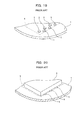
FIGS. 18(a) and 18(b) , thethermoset resin 5 is applied to aposition 6 on thesubstrate 1 where thesemiconductor package component 3 is to be mounted.FIG. 19 illustrates how thethermoset resin 5 is applied. - In
FIG. 18(c) , thesemiconductor package component 3 is mounted on thesubstrate 1 in such a manner that thebump electrodes 4 of thesemiconductor package component 3 come into contact with theelectrode 2 on thesubstrate 1. At this point, theuncured thermoset resin 5 is in contact with thesubstrate 1 and the underside of thesemiconductor package component 3. - In
FIG. 18(d) , reflow is performed. In the reflow, the solder of thebump electrodes 4 melts. Since thethermoset resin 5 is uncured at this point in time, thesemiconductor package component 3 is moved to the proper position by the self-alignment effect of the melted solder between the electrodes on thesubstrate 1 and the electrodes of thesemiconductor package component 3. After thethermoset resin 5 is cured by heating, the temperature decreases to a temperature not higher than the melting temperature of the solder to solidify the solder, so that the electrical connection and mechanical bonding of thesemiconductor package component 3 to thesubstrate 1 are completed.FIG. 20 illustrates the completion of the mounting. -
- Patent Literature: Japanese Patent Application Laid-Open Publication No.
11-204568 - The mounting process illustrated in
FIGS. 18 to 20 involves only one heating step. However, the quantity and position of thethermoset resin 5 to be applied are difficult to adjust, thereby causing variations in mounting quality. - Specifically, during the process in which the solder melts and solidifies, the
uncured thermoset resin 5 is in the vicinity of or in contact with the solder. Therefore, when the application quantity of thethermoset resin 5 is reduced in order to prevent some of theuncured thermoset resin 5 from melting and being mixed with the solidifying solder to degrade the soldering quality, the strength of the mechanical bonding between thesemiconductor package component 3 and thesubstrate 1 decreases. - An object of the present invention is to provide a semiconductor package component mounting method which can reduce the number of heating steps, stably maintain the quality of electrical joining between a semiconductor package component and a substrate, and ensure a sufficient strength of mechanical bonding between the semiconductor package component and the substrate.
- A semiconductor package component mounting method according to the present invention includes: mounting a semiconductor package component on a substrate in such a manner that an electrode of the substrate and an electrode of the semiconductor package component are brought into contact with each other through a solidified joining metal; applying a reinforcing adhesive between the periphery of an area on the substrate where the semiconductor package component is mounted and the outer surface of the semiconductor package component in such a manner that the reinforcing adhesive does not contact the joining metal; and performing reflow to melt the joining metal while the reinforcing adhesive is uncured, curing the reinforcing adhesive, and solidifying the joining metal.
- A semiconductor package component mounting structure according to the present invention is a structure in which a semiconductor package component is mounted onto a substrate by joining an electrode of the substrate to an electrode of the semiconductor package component with a joining metal. The mounting structure includes: a cured reinforcing adhesive which is not in contact with the joining metal, the reinforcing adhesive extending from a surface of the semiconductor package component opposite a surface facing the substrate to the substrate, wherein the cured reinforcing adhesive extends over a distance L1 onto the opposite surface of the semiconductor package component from an end face of the semiconductor package component and extends over a distance L2 onto the surface of the semiconductor package component facing the substrate from the end face of the semiconductor package component, the end face connecting the surface of the semiconductor package component facing the substrate and the opposite surface; and the distance L1 over which the reinforcing adhesive extends onto the opposite surface of the semiconductor package component from the end face connecting the surface of the semiconductor package component facing the substrate and the opposite surface is equal to or greater than the distance L2 over which the reinforcing adhesive extends onto the surface of the semiconductor package component facing the substrate from the end face of the semiconductor package component.
- A semiconductor package component mounting method according to the present invention includes: applying a first reinforcing adhesive to a position on a substrate where a semiconductor package component is to be mounted; mounting the semiconductor package component on the substrate in such a manner that an electrode of the substrate and an electrode of the semiconductor package component are brought into contact with each other through a solidified joining metal; applying a second reinforcing adhesive between the periphery of an area on the substrate where the semiconductor package component is mounted and the outer surface of the semiconductor package component; and performing reflow to melt the joining metal and curing the first and second reinforcing adhesives while the joining metal solidifies.
- A semiconductor package component mounting structure according to the present invention is a structure in which a semiconductor package component is mounted on a substrate by joining an electrode of the substrate to an electrode of the semiconductor package component with a joining metal. The mounting structure includes: a cured first reinforcing adhesive disposed between the substrate and a surface of the semiconductor package component facing the substrate; and a cured second reinforcing adhesive disposed from an end face connecting the surface of the semiconductor package component facing the substrate and the opposite surface of the semiconductor package component to the substrate.
- A semiconductor package component mounting structure according to the present invention is a structure in which a semiconductor package component is mounted on a substrate by joining an electrode of the substrate to an electrode of the semiconductor package component with a joining metal. The mounting structure includes: a cured first reinforcing adhesive disposed between the substrate and a surface of the semiconductor package component facing the substrate; and a cured second reinforcing adhesive disposed from the surface of the semiconductor package component opposite the surface facing the substrate to the substrate.
- With this configuration, since the reinforcing adhesive is applied after the semiconductor package component is mounted on the substrate, and in the heating step, the reinforcing adhesive is sufficiently cured after the joining metal has melts and solidifies. Thus the number of heating steps can be reduced and the reinforcing adhesive can be readily applied in such a manner that the reinforcing adhesive does not come into contact with the joining metal in the process of melting and solidifying. In addition, the quality of electrical joining between the semiconductor package component and the substrate can be stably maintained, and a sufficient strength of the mechanical bonding between the semiconductor package component and the substrate can be ensured.
- With this configuration, the first reinforcing adhesive is applied before the semiconductor package component is mounted on the substrate; the second reinforcing adhesive is applied after the semiconductor package component is mounted on the substrate; and, in the heating step, the first and second reinforcing adhesives are cured after the joining metal melts and solidifies. Accordingly, the number of heating steps can be reduced and, even when the application quantity of the first reinforcing adhesive is reduced in order to prevent degradation of the joining quality due to some of the first reinforcing adhesive mixed during the melting of the joining metal, the cured second reinforcing adhesive ensures a sufficient mechanical strength.
-
-
FIG. 1 is a process diagram illustrating a mounting method according to a first embodiment of the present invention; -
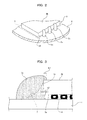
FIG. 2 is a perspective view illustrating a reinforcing adhesive applied according to the first embodiment; -
FIG. 3 is a cross-sectional view illustrating completion of mounting according to the first embodiment; -
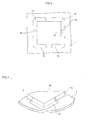
FIG. 4 is a plan view of a mounting method according to a second embodiment of the present invention; -
FIG. 5 is a perspective view illustrating completion of mounting according to the second embodiment; -
FIG. 6 is a plan view of a mounting method according to a third embodiment of the present invention; -
FIG. 7 is a perspective view illustrating completion of mounting according to the third embodiment; -
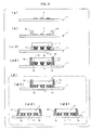
FIG. 8 is a process diagram of a mounting method according to a fourth embodiment of the present invention; -
FIG. 9 is a perspective view illustrating first and second reinforcing adhesives applied according to the fourth embodiment; -
FIG. 10 is a cross-sectional view illustrating completion of mounting according to the fourth embodiment; -
FIG. 11 is a horizontal cross-sectional view illustrating the first and second reinforcing adhesives applied according to the fourth embodiment; -
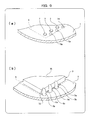
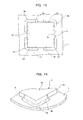
FIG. 12 is a plan view illustrating completion of mounting of a mounting method according to a fifth embodiment of the present invention; -
FIG. 13 is a perspective view illustrating the completion of mounting according to the fifth embodiment; -
FIG. 14 is a horizontal cross-sectional view illustrating the completion of mounting according to the fifth embodiment; -
FIG. 15 is a plan view illustrating completion of mounting of a mounting method according to a sixth embodiment of the present invention; -
FIG. 16 is a perspective view illustrating the completion of mounting according to the sixth embodiment; -
FIG. 17 is a process diagram illustrating a conventional mounting method; -
FIG. 18 is a process diagram illustrating another conventional mounting method; -
FIG. 19 is a perspective view illustrating the method inFIG. 18(b) ; -
FIG. 20 is a perspective view illustrating the method inFIG. 18(c) ; and -
FIG. 21 is a cross-sectional view of a variation of the third embodiment. - A semiconductor package component mounting method of the present invention will be described below with respect to specific embodiments.
-
FIGS. 1 to 3 illustrate a first embodiment of the present invention. - In
FIGS. 1(a) and 1(b) , a BGAsemiconductor package component 3 is mounted on asubstrate 1 in such a manner that bumpelectrodes 4 of thesemiconductor package component 3 come into contact withelectrodes 2 on thesubstrate 1. - In
FIG. 1(c) , reinforcingadhesives 5c are applied in the form of a stick from the periphery of an area on thesubstrate 1 where thesemiconductor package component 3 is mounted over to the outer surface of thesemiconductor package component 3 at regular intervals except the corner portions as illustrated inFIG. 2 . This arrangement can reduce the application quantity of the adhesive and prevent the adhesive from unnecessarily entering between thesemiconductor package component 3 and the substrate. Since the reinforcingadhesives 5c are applied in the form of a stick at regular intervals except the corner portions, thesemiconductor package component 3 can be fixed in a balanced manner. The reinforcing adhesive 5c herein is a thermoset resin. The reinforcing adhesive 5c is applied in such a manner that the reinforcing adhesive 5c does not contact thebump electrodes 4. - In
FIG. 1(d) , reflow is performed. In the reflow, the solder of thebump electrodes 4 melts. Since the reinforcing adhesive 5c is not cured at this point, thesemiconductor package component 3 is moved to a proper position by the self-alignment effect of the melted solder between the electrodes on thesubstrate 1 and the electrodes of thesemiconductor package component 3. - In
FIG. 1(e) , the temperature further rises to cure the reinforcing adhesive 5c. Then the temperature is decreased to the melting temperature of the solder or lower to solidify the solder, thereby completing the electrical connection and mechanical bonding of thesemiconductor package component 3 and thesubstrate 1. - In the completed mounting structure of
FIG. 3 , the reinforcing adhesive 5c can be readily prevented from contacting thebump electrodes 4 even if the application quantities and application positions are varied. This is because thesemiconductor package component 3 is mounted on thesubstrate 1 as illustrated inFIG. 1(b) and then the reinforcing adhesive 5c is applied so that the reinforcing adhesive 5c extends from asurface 3b of thesemiconductor package component 3 opposite asurface 3a facing thesubstrate 1 to thesubstrate 1 as illustrated inFIG. 1(c) . As illustrated inFIG. 3 , in the completed mounting structure, the reinforcing adhesive 5c is away from the solder which is a joining metal. Thus, good soldering quality is achieved. A portion L1 is convex-shaped. While a portion L2 is concave-shaped, the portion L2 may be convex-shaped. - The shape of the cured reinforcing adhesive 5c is made such that L1 ≥ L2, where L1 is a distance over which the reinforcing adhesive 5c extends onto the
surface 3b of thesemiconductor package component 3 opposite thesurface 3a facing thesubstrate 1 from anend face 3c connecting thesurface 3a and thesurface 3b, and L2 is a distance over which the reinforcing adhesive 5c extends onto thesurface 3a facing thesubstrate 1 from theend face 3c of thesemiconductor package component 3. As a result, a great degree of reinforcement is achieved compared with a structure in which the reinforcing adhesive 5c is applied from theend face 3c of thesemiconductor package component 3 to thesubstrate 1 as indicated by aphantom line 7 inFIG. 3 in the step ofFIG. 1(c) and then cured by reflow. - It should be noted that even when the reinforcing adhesive 5c is cured in the shape indicated by the
phantom line 7 inFIG. 3 , better soldering quality and a greater degree of reinforcement are achieved than in the conventional example illustrated inFIGS. 9 to 11 . - A gap between the
substrate 1 and thesemiconductor package component 3 in this case is approximately 0.2 mm. The melting point and solidification start temperature of the solder of thebump electrodes 4 were in the range of 217°C to 219°C and 219°C, respectively. The viscosity of the reinforcing adhesive 5c was 60 Pa · s (measured with a cone and plate viscometer at 5 rpm and 25°C). The curing start temperature of the reinforcing adhesive 5c was 185°C and the curing peak temperature of the reinforcing adhesive 5c was 210°C. - The thixotropy of the reinforcing adhesive 5c determined from a ratio between viscosities measured with the cone and plate viscometer at 0.5 rpm and 5 rpm at 25°C (viscosity at 0.5 rpm/viscosity at 5 rpm) was in the range of approximately 4 to 6.
-
FIGS. 4 and 5 illustrate a second embodiment. - In the first embodiment, the reinforcing adhesive 5c is applied to a portion except the
corner portions 3d of thesemiconductor package component 3 and cured. In the second embodiment, in the step ofFIG. 1(c) , a reinforcing adhesive 5c is applied to portions of asemiconductor package component 3 includingcorner portions 3d, and distances L1 and L2 of the cured reinforcing adhesive 5c are set such that L1 ≥ L2. The second embodiment is different from the first embodiment only in the shape of the applied reinforcing adhesive 5c. Others are the same as in the embodiment. - In the second embodiment, better soldering quality and a greater degree of reinforcement than in the first embodiment are achieved.
-
FIGS. 6 and 7 illustrate a third embodiment. - In the second embodiment, the reinforcing adhesive 5c is applied to the portions of the
semiconductor package component 3 including thecorner portions 3d of thesemiconductor package component 3 in such a manner that L1 ≥ L2. The third embodiment differs from the second embodiment in that L1 = 0. Specifically, the third embodiment differs from the first embodiment only in that a reinforcing adhesive 5c is applied in such a manner that the reinforcing adhesive 5c extends from anend face 3c that connecting asurface 3a of asemiconductor package component 3 facing asubstrate 1 and anopposite surface 3b to thesubstrate 1. Others are the same as in the first embodiment. - The reinforcing adhesive 5c is applied from the
end face 3c of thesemiconductor package component 3 to cover the full height of theend face 3c of thesemiconductor package component 3 in a position where the reinforcing adhesive 5c is applied and the surface of the reinforcing adhesive 5c outside from theend face 3c of thesemiconductor package component 3 is concave-shaped along the height of theend face 3c as illustrated inFIG. 21 . A distance L3 from the edge of thesemiconductor package component 3 to the perimeter of the reinforcing adhesive 5c is preferably greater than a distance L4 from thesubstrate 1 to the top of thesemiconductor package component 3. - While the shape of the surface of the reinforcing adhesive 5c outside from the end face 3c is concave-shaped along the height of the
end face 3c inFIGS. 7 and21 , the completed shape of the surface of the reinforcing adhesive 5c may be convex-shaped as indicated by a phantom line inFIG. 21 , depending on the viscosity of the used reinforcing adhesive 5c. - According to the embodiment, better soldering quality and a greater degree of reinforcement than in the conventional art are achieved.
- While the embodiments have been described with respect to BGA
semiconductor package components 3 by way of example, the embodiments are also applicable to LGA (Land Grid Array)semiconductor package components 3. In the case of the LGAsemiconductor package component 3, a paste containing a joining metal is applied to at least one of a set of electrodes of thesemiconductor package component 3 and a set ofelectrodes 2 of asubstrate 1 to be joined to the set of the electrodes of thesemiconductor package component 3. Then thesemiconductor package component 3 can be mounted on thesubstrate 1 to implement the present invention. -
FIGS. 8 to 11 illustrate a fourth embodiment of the present invention. - In
FIG. 8(a) and 8(b) , afirst thermoset resin 5a is applied in the form of a dot in aposition 6 on asubstrate 1 where asemiconductor package component 3 is to be mounted.FIG. 9 illustrates how thefirst thermoset resin 5a is applied. - In
FIG. 8(c) , thesemiconductor package component 3 is mounted on thesubstrate 1 in such a manner that bumpelectrodes 4 of thesemiconductor package component 3 come into contact withelectrodes 2 on thesubstrate 1. At this point, the uncuredfirst thermoset resin 5a is disposed between and in contact with thesubstrate 1 and the underside of thesemiconductor package component 3. - In
FIG. 8 (c-1), thesemiconductor package component 3 is mounted on thesubstrate 1 in such a manner that thebump electrodes 4 of the BGAsemiconductor package component 3 come into contact with theelectrodes 2 on thesubstrate 1. - In
FIG. 8 (c-2), a second reinforcing adhesive 5b is applied between the periphery of the area on thesubstrate 1 where thesemiconductor package component 3 is mounted and the outer surface of thesemiconductor package component 3, for example, at predetermined intervals, as illustrated inFIG. 9(b) . Here, the second reinforcing adhesive 5b is a thermoset resin. - In
FIG. 8(d) , reflow is performed. -
FIG. 8(d) includesFIGS. 8 (d-1), 8(d-2) and 8(d-3).FIGS. 8 (d-2) and 8(d-3) depict cross sections as viewed from different angles at the same point in time in the reflow to show how the first and second reinforcingadhesives FIG. 8 (d-1) . - In
FIG. 8 (d-1), the solder of thebump electrodes 4 is melted by the reflow. Since the first and second reinforcingadhesives semiconductor package component 3 moves to a proper position by the self-alignment effect of the melted solder between theelectrodes 2 of thesubstrate 1. and the electrodes of thesemiconductor package component 3. - After the temperature further rises and the first and second reinforcing
adhesives FIGS. 8 (d-2) and 8(d-3), the temperature is decreased to the melting point of the solder or lower to solidify the solder, thereby completing the electrical connection and mechanical bonding of thesemiconductor package component 3 and thesubstrate 1.FIG. 10 is a vertical cross-sectional view illustrating the completion of the mounting.FIG. 11 is a cross-sectional view taken horizontally along a plane of theelectrodes 2 of thesubstrate 1. - In the mounting structure completed as illustrated in
FIG. 10 , since thesemiconductor package component 3 is mounted on thesubstrate 1 and then the second reinforcing adhesive 5b is applied from asurface 3b opposite asurface 3a of thesemiconductor package component 3 facing thesubstrate 1 to thesubstrate 1 as illustrated inFIG. 8 (c-2), strong joining between thesubstrate 1 and thesemiconductor package component 3 can be provided by the cured second reinforcing adhesive 5b even when the quantity of the first reinforcing adhesive 5a is reduced to prevent the first reinforcing adhesive 5a from contacting the solder, and strong joining may not be provided by the first reinforcing adhesive 5a between thesubstrate 1 and thepackage component 3. In addition, since the second reinforcing adhesive 5b is applied after thesemiconductor package component 3 is mounted on thesubstrate 1, the second reinforcing adhesive 5b is distanced from the solder which is a joining metal, irrespective of variations of the application quantity and application positions, as illustrated inFIG. 10 . Thus, good soldering quality is achieved. - The shape of the cured second reinforcing adhesive 5b is made such that L1 > L2, where L1 is a distance over which the second reinforcing adhesive 5b extends onto the
surface 3b of thesemiconductor package component 3 opposite thesurface 3a facing thesubstrate 1 from anend face 3c connecting thesurface 3a and thesurface 3b, and L2 is a distance over which the second reinforcing adhesive 5b extends onto thesurface 3a facing thesubstrate 1 from theend face 3c of thesemiconductor package component 3. As a result, a greater degree of reinforcement is achieved compared with a structure in which the second reinforcing adhesive 5b is applied from theend face 3c of thesemiconductor package component 3 to thesubstrate 1 as indicated by aphantom line 7 inFIG. 10 in the step ofFIG. 8(c) and then cured by reflow. - It should be noted that even when the second reinforcing adhesive 5b is cured in the shape represented by the
phantom line 7 inFIG. 10 , better soldering quality and a greater degree of reinforcement are achieved than in the conventional example illustrated inFIGS. 18 to 20 . - A gap between the
substrate 1 and thesemiconductor package component 3 at that point was approximately 0.2 mm. The melting point and solidification start temperature of the solder of thebump electrodes 4 were in the range of 217°C to 219°C and 219°C, respectively. The viscosity of the reinforcing adhesive 5a was 60 Pa · s (measured with a cone and plate viscometer at 5 rpm and 25°C). The curing start temperature of the reinforcing adhesive 5a was 185°C and the curing peak temperature of the reinforcing adhesive 5a was 210°C. -
FIGS. 12 to 14 illustrate a fifth embodiment. - In the fourth embodiment, the second reinforcing adhesive 5b is applied to portions of the
semiconductor package component 3 except thecorner portions 3d. In the fifth embodiment, a second reinforcing adhesive 5b is applied to portions of asemiconductor package component 3 includingcorner portions 3d of thesemiconductor package component 3 in the step ofFIG. 8 (c-2). Distances L1 and L2 of the cured second reinforcing adhesive 5b are set such that L1 ≥ L2. The fifth embodiment is different from the fourth embodiment only in the shape of the applied second reinforcing adhesive 5b. Others are the same as in the fourth embodiment. - According to the fifth embodiment, good soldering quality and a greater degree of reinforcement than in the fourth embodiment are achieved as illustrated in
FIG. 13 .FIG. 14 is a horizontal cross-sectional view of a first reinforcing adhesive 5a and the second reinforcing adhesive 5b which are cured. -
FIGS. 15 and 16 illustrate a sixth embodiment. - In the fifth embodiment, the second reinforcing adhesive 5b is applied to the portions of the
semiconductor package component 3 including thecorner portions 3d of thesemiconductor package component 3 in such a manner that L1 ≥ L2. The sixth embodiment differs from the fifth embodiment in that L1 = 0. Specifically, the sixth embodiment is different from the fourth embodiment only in that a second reinforcing adhesive 5b is applied in such a manner that the second reinforcing adhesive 5b extends from anend face 3c connecting asurface 3a of asemiconductor package component 3 facing asubstrate 1 and anopposite surface 3b to thesubstrate 1. Others are the same as in the fourth embodiment. - According to the embodiment, good soldering quality and a greater degree of reinforcement than in the fourth embodiment are achieved.
- While the embodiments have been described with respect to BGA
semiconductor package components 3 by way of example, the embodiments are also applicable to LGA (Land Grid Array)semiconductor package components 3. In the case of the LGAsemiconductor package component 3, a paste containing a joining metal is applied to at least one of a set of electrodes of thesemiconductor package component 3 and a set ofelectrodes 2 of asubstrate 1 to be joined to the set of the electrodes of thesemiconductor package component 3. Then thesemiconductor package component 3 can be mounted on thesubstrate 1 to implement the present invention. - The present invention is useful for fabrication of various electronic devices such as mobile devices that may be subjected to drop impact.
Claims (12)
- A semiconductor package component mounting method comprising:mounting a semiconductor package component on a substrate in such a manner that an electrode of the substrate and an electrode of the semiconductor package component are brought into contact with each other through a solidified joining metal;applying a reinforcing adhesive between a periphery of an area on the substrate where the semiconductor package component is mounted and an outer surface of the semiconductor package component in such a manner that the reinforcing adhesive does not contact the joining metal; andperforming reflow to melt the joining metal while the reinforcing adhesive is uncured, curing the reinforcing adhesive, and solidifying the joining metal.
- The semiconductor package component mounting method according to claim 1, wherein, in the applying of the reinforcing adhesive, the reinforcing adhesive is applied so that the reinforcing adhesive extends from a surface of the semiconductor package component opposite a surface facing the substrate to the substrate.
- The semiconductor package component mounting method according to claim 1, wherein, in the applying of the reinforcing adhesive, the reinforcing adhesive is applied so that the reinforcing adhesive extends from an end face of the semiconductor package component to the substrate, the end face connecting a surface of the semiconductor package component facing the substrate and a surface opposite the surface.
- A semiconductor package component mounting structure in which a semiconductor package component is mounted on a substrate by joining an electrode of the substrate to an electrode of the semiconductor package component with a joining metal, the mounting structure comprising:a cured reinforcing adhesive which is not in contact with the joining metal, the reinforcing adhesive extending from a surface of the semiconductor package component opposite a surface facing the substrate to the substrate, wherein:the cured reinforcing adhesive extends over a distance L1 onto the opposite surface of the semiconductor package component from an end face of the semiconductor package component and extends over a distance L2 onto the surface of the semiconductor package component facing the substrate from the end face of the semiconductor package component, the end face connecting the surface of the semiconductor package component facing the substrate and the opposite surface; andthe distance L1 over which the reinforcing adhesive extends onto the opposite surface of the semiconductor package component from the end face connecting the surface of the semiconductor package component facing the substrate and the opposite surface is equal to or greater than the distance L2 over which the reinforcing adhesive extends onto the surface of the semiconductor package component facing the substrate from the end face of the semiconductor package component.
- The semiconductor package component mounting structure according to claim 4, wherein the reinforcing adhesive is not in contact with the joining metal.
- A semiconductor package component mounting method comprising:applying a first reinforcing adhesive to a position on a substrate where a semiconductor package component is to be mounted;mounting the semiconductor package component on the substrate in such a manner that an electrode of the substrate and an electrode of the semiconductor package component are brought into contact with each other through a solidified joining metal;applying a second reinforcing adhesive between a periphery of an area on the substrate where the semiconductor package component is mounted and an outer surface of the semiconductor package component; andperforming reflow to melt the joining metal and curing the first and second reinforcing adhesives while the joining metal solidifies.
- The semiconductor package component mounting method according to claim 1, wherein, in the applying of the second reinforcing adhesive, the second reinforcing adhesive is applied so that the second reinforcing adhesive extends from a surface of the semiconductor package component opposite a surface facing the substrate to the substrate.
- The semiconductor package component mounting method according to claim 1, wherein, in the applying of the second reinforcing adhesive, the second reinforcing adhesive is applied so that the second reinforcing adhesive extends from an end face of the semiconductor package component to the substrate, the end face connecting a surface of the semiconductor package component facing the substrate and a surface opposite the surface.
- A semiconductor package component mounting structure in which a semiconductor package component is mounted on a substrate by joining an electrode of the substrate to an electrode of the semiconductor package component with a joining metal, the mounting structure comprising:a cured first reinforcing adhesive disposed between the substrate and a surface of the semiconductor package component facing the substrate; anda cured second reinforcing adhesive disposed from an end face connecting the surface of the semiconductor package component facing the substrate and an opposite surface of the semiconductor package component to the substrate.
- The semiconductor package component mounting structure according to claim 9, wherein the first and second reinforcing adhesives are not in contact with the joining metal.
- A semiconductor package component mounting structure in which a semiconductor package component is mounted on a substrate by joining an electrode of the substrate to an electrode of the semiconductor package component with a joining metal, the mounting structure comprising:a cured first reinforcing adhesive disposed between the substrate and a surface of the semiconductor package component facing the substrate; anda cured second reinforcing adhesive disposed from a surface of the semiconductor package component opposite the surface facing the substrate to the substrate.
- The semiconductor package component mounting structure according to claim 11, wherein the first and second reinforcing adhesives are not in contact with the joining metal.
Applications Claiming Priority (3)
| Application Number | Priority Date | Filing Date | Title |
|---|---|---|---|
| JP2009105758A JP5464897B2 (en) | 2009-04-24 | 2009-04-24 | Mounting method and mounting structure for semiconductor package components |
| JP2009105757A JP5707569B2 (en) | 2009-04-24 | 2009-04-24 | Mounting method and mounting structure for semiconductor package components |
| PCT/JP2010/002800 WO2010122757A1 (en) | 2009-04-24 | 2010-04-19 | Method for mounting semiconductor package component, and structure having semiconductor package component mounted therein |
Publications (4)
| Publication Number | Publication Date |
|---|---|
| EP2423955A1 true EP2423955A1 (en) | 2012-02-29 |
| EP2423955A4 EP2423955A4 (en) | 2013-04-10 |
| EP2423955B1 EP2423955B1 (en) | 2019-09-04 |
| EP2423955B8 EP2423955B8 (en) | 2019-10-09 |
Family
ID=43010884
Family Applications (1)
| Application Number | Title | Priority Date | Filing Date |
|---|---|---|---|
| EP10766819.6A Active EP2423955B8 (en) | 2009-04-24 | 2010-04-19 | Method for mounting semiconductor package component, and structure having semiconductor package component mounted therein |
Country Status (4)
| Country | Link |
|---|---|
| US (2) | US20110108997A1 (en) |
| EP (1) | EP2423955B8 (en) |
| CN (1) | CN102105971B (en) |
| WO (1) | WO2010122757A1 (en) |
Families Citing this family (11)
| Publication number | Priority date | Publication date | Assignee | Title |
|---|---|---|---|---|
| JP5658088B2 (en) * | 2011-05-23 | 2015-01-21 | パナソニックIpマネジメント株式会社 | Semiconductor package component mounting structure and manufacturing method |
| JP5719999B2 (en) * | 2011-05-26 | 2015-05-20 | パナソニックIpマネジメント株式会社 | Electronic component mounting method, electronic component mounting apparatus, and electronic component mounting system |
| JP5942308B2 (en) * | 2012-09-06 | 2016-06-29 | パナソニックIpマネジメント株式会社 | Mounting structure and method for supplying reinforcing resin material |
| US10823355B2 (en) * | 2016-01-27 | 2020-11-03 | Lite-On Electronics (Guangzhou) Limited | Light-emitting module for vehicle lamp |
| TWM521008U (en) * | 2016-01-27 | 2016-05-01 | 光寶科技股份有限公司 | Lamp device and its lighting module |
| KR102694680B1 (en) * | 2016-08-01 | 2024-08-14 | 삼성디스플레이 주식회사 | Electronic device, mounting method of the same, and method of manufacturing display apparatus having the same |
| US10211072B2 (en) * | 2017-06-23 | 2019-02-19 | Applied Materials, Inc. | Method of reconstituted substrate formation for advanced packaging applications |
| EP3706171A4 (en) * | 2017-11-01 | 2021-04-21 | Sony Semiconductor Solutions Corporation | IMAGING ELEMENT, IMAGING DEVICE, ELECTRONIC APPARATUS, AND IMAGING ELEMENT MANUFACTURING METHOD |
| US10957672B2 (en) * | 2017-11-13 | 2021-03-23 | Taiwan Semiconductor Manufacturing Company, Ltd. | Package structure and method of manufacturing the same |
| US11094668B2 (en) * | 2019-12-12 | 2021-08-17 | Micron Technology, Inc. | Solderless interconnect for semiconductor device assembly |
| JP7283407B2 (en) * | 2020-02-04 | 2023-05-30 | 株式会社デンソー | electronic device |
Family Cites Families (52)
| Publication number | Priority date | Publication date | Assignee | Title |
|---|---|---|---|---|
| JPH07131145A (en) | 1993-11-08 | 1995-05-19 | Matsushita Electric Ind Co Ltd | Soldering method for electronic parts |
| US5866953A (en) * | 1996-05-24 | 1999-02-02 | Micron Technology, Inc. | Packaged die on PCB with heat sink encapsulant |
| US6274389B1 (en) * | 1997-01-17 | 2001-08-14 | Loctite (R&D) Ltd. | Mounting structure and mounting process from semiconductor devices |
| US5891753A (en) * | 1997-01-24 | 1999-04-06 | Micron Technology, Inc. | Method and apparatus for packaging flip chip bare die on printed circuit boards |
| US5814401A (en) * | 1997-02-04 | 1998-09-29 | Motorola, Inc. | Selectively filled adhesive film containing a fluxing agent |
| US6507116B1 (en) * | 1997-04-24 | 2003-01-14 | International Business Machines Corporation | Electronic package and method of forming |
| US5895229A (en) * | 1997-05-19 | 1999-04-20 | Motorola, Inc. | Microelectronic package including a polymer encapsulated die, and method for forming same |
| JPH11163049A (en) | 1997-11-28 | 1999-06-18 | Matsushita Electric Ind Co Ltd | Mounting structure and mounting method of electronic component with bump |
| US5936304A (en) * | 1997-12-10 | 1999-08-10 | Intel Corporation | C4 package die backside coating |
| US6049124A (en) * | 1997-12-10 | 2000-04-11 | Intel Corporation | Semiconductor package |
| JP3417281B2 (en) | 1998-01-08 | 2003-06-16 | 松下電器産業株式会社 | How to mount electronic components with bumps |
| US6046910A (en) * | 1998-03-18 | 2000-04-04 | Motorola, Inc. | Microelectronic assembly having slidable contacts and method for manufacturing the assembly |
| US20020014688A1 (en) * | 1999-03-03 | 2002-02-07 | Suresh Ramalingam | Controlled collapse chip connection (c4) integrated circuit package which has two dissimilar underfill materials |
| JP2000260912A (en) * | 1999-03-05 | 2000-09-22 | Fujitsu Ltd | Semiconductor device mounting structure and semiconductor device mounting method |
| JP3890814B2 (en) | 1999-05-25 | 2007-03-07 | 株式会社デンソー | Electronic component mounting method |
| US6700209B1 (en) * | 1999-12-29 | 2004-03-02 | Intel Corporation | Partial underfill for flip-chip electronic packages |
| US6441485B1 (en) * | 2000-05-11 | 2002-08-27 | Amkor Technology, Inc. | Apparatus for electrically mounting an electronic device to a substrate without soldering |
| US6576495B1 (en) * | 2000-08-30 | 2003-06-10 | Micron Technology, Inc. | Microelectronic assembly with pre-disposed fill material and associated method of manufacture |
| US6340846B1 (en) * | 2000-12-06 | 2002-01-22 | Amkor Technology, Inc. | Making semiconductor packages with stacked dies and reinforced wire bonds |
| JP2002198384A (en) * | 2000-12-27 | 2002-07-12 | Matsushita Electric Ind Co Ltd | Semiconductor device and method of manufacturing semiconductor device |
| US6545869B2 (en) * | 2001-01-17 | 2003-04-08 | International Business Machines Corporation | Adjusting fillet geometry to couple a heat spreader to a chip carrier |
| TW527676B (en) * | 2001-01-19 | 2003-04-11 | Matsushita Electric Industrial Co Ltd | Photo-semiconductor module and method for manufacturing |
| US6570259B2 (en) * | 2001-03-22 | 2003-05-27 | International Business Machines Corporation | Apparatus to reduce thermal fatigue stress on flip chip solder connections |
| US6562663B2 (en) * | 2001-03-28 | 2003-05-13 | Motorola, Inc. | Microelectronic assembly with die support and method |
| US6486554B2 (en) * | 2001-03-30 | 2002-11-26 | International Business Machines Corporation | Molded body for PBGA and chip-scale packages |
| JP3565204B2 (en) * | 2001-12-28 | 2004-09-15 | 三菱電機株式会社 | Electronic equipment |
| JP3948289B2 (en) | 2002-01-22 | 2007-07-25 | 松下電器産業株式会社 | Electronic component mounting method |
| US20040238925A1 (en) * | 2003-05-23 | 2004-12-02 | Paul Morganelli | Pre-applied thermoplastic reinforcement for electronic components |
| US20040262368A1 (en) * | 2003-06-26 | 2004-12-30 | Haw Tan Tzyy | Ball grid array solder joint reliability |
| JP2005032795A (en) | 2003-07-08 | 2005-02-03 | Matsushita Electric Ind Co Ltd | Electronic component mounting structure and electronic component mounting method |
| JP3912342B2 (en) | 2003-07-08 | 2007-05-09 | 松下電器産業株式会社 | Electronic component mounting method |
| US20050077080A1 (en) * | 2003-10-14 | 2005-04-14 | Adesoji Dairo | Ball grid array (BGA) package having corner or edge tab supports |
| US7064452B2 (en) * | 2003-11-04 | 2006-06-20 | Tai-Saw Technology Co., Ltd. | Package structure with a retarding structure and method of making same |
| JP4605155B2 (en) * | 2004-03-29 | 2011-01-05 | 日本電気株式会社 | Semiconductor device and manufacturing method thereof |
| JP2006339316A (en) * | 2005-05-31 | 2006-12-14 | Toshiba Corp | Semiconductor device, semiconductor device mounting substrate, and semiconductor device mounting method |
| JP2007048976A (en) * | 2005-08-10 | 2007-02-22 | Toshiba Corp | Printed circuit board and electronic device provided with printed circuit board |
| US7682879B2 (en) * | 2006-03-28 | 2010-03-23 | Seagate Technology Llc | Edge coating a microelectronic device |
| US20080036097A1 (en) * | 2006-08-10 | 2008-02-14 | Teppei Ito | Semiconductor package, method of production thereof and encapsulation resin |
| JP2008053347A (en) | 2006-08-23 | 2008-03-06 | Seiko Epson Corp | Device, manufacturing method thereof, circuit board, and electronic apparatus |
| US7843074B2 (en) * | 2006-09-12 | 2010-11-30 | Lumination Llc | Underfill for light emitting device |
| JP5085081B2 (en) | 2006-09-22 | 2012-11-28 | パナソニック株式会社 | Electronic component mounting structure |
| JP2008166377A (en) * | 2006-12-27 | 2008-07-17 | Toshiba Corp | Printed circuit board manufacturing method, printed circuit board, and reinforced electronic component |
| JP2008300538A (en) | 2007-05-30 | 2008-12-11 | Toshiba Corp | Printed circuit board, printed circuit board manufacturing method, and electronic device |
| JP2008311458A (en) * | 2007-06-15 | 2008-12-25 | Panasonic Corp | Semiconductor device mounting structure, method for manufacturing the same, and method for peeling semiconductor device |
| US7993984B2 (en) * | 2007-07-13 | 2011-08-09 | Panasonic Corporation | Electronic device and manufacturing method |
| JP2009021465A (en) * | 2007-07-13 | 2009-01-29 | Panasonic Corp | Semiconductor device mounting structure, method for manufacturing the same, and method for peeling semiconductor device |
| US7919356B2 (en) * | 2007-07-31 | 2011-04-05 | International Business Machines Corporation | Method and structure to reduce cracking in flip chip underfill |
| JP2009135150A (en) * | 2007-11-28 | 2009-06-18 | Toshiba Corp | Printed circuit board, printed circuit board manufacturing method, and electronic device |
| JP4696227B2 (en) * | 2007-12-28 | 2011-06-08 | スパンション エルエルシー | Manufacturing method of semiconductor device |
| JP4621778B2 (en) * | 2009-01-29 | 2011-01-26 | 株式会社東芝 | Electronic equipment and circuit board |
| JP4676012B2 (en) * | 2009-06-03 | 2011-04-27 | 株式会社東芝 | Electronics |
| US8129230B2 (en) * | 2009-08-11 | 2012-03-06 | International Business Machines Corporation | Underfill method and chip package |
-
2010
- 2010-04-19 EP EP10766819.6A patent/EP2423955B8/en active Active
- 2010-04-19 US US13/003,996 patent/US20110108997A1/en not_active Abandoned
- 2010-04-19 CN CN2010800022176A patent/CN102105971B/en active Active
- 2010-04-19 WO PCT/JP2010/002800 patent/WO2010122757A1/en not_active Ceased
-
2013
- 2013-11-27 US US14/092,407 patent/US9331047B2/en active Active
Also Published As
| Publication number | Publication date |
|---|---|
| CN102105971A (en) | 2011-06-22 |
| US20140120663A1 (en) | 2014-05-01 |
| EP2423955B1 (en) | 2019-09-04 |
| EP2423955A4 (en) | 2013-04-10 |
| US9331047B2 (en) | 2016-05-03 |
| EP2423955B8 (en) | 2019-10-09 |
| US20110108997A1 (en) | 2011-05-12 |
| CN102105971B (en) | 2013-05-22 |
| WO2010122757A1 (en) | 2010-10-28 |
Similar Documents
| Publication | Publication Date | Title |
|---|---|---|
| EP2423955B1 (en) | Method for mounting semiconductor package component, and structure having semiconductor package component mounted therein | |
| US20150371931A1 (en) | Semiconductor device and method for producing same | |
| CN104246997B (en) | Assembling structure and its manufacture method | |
| JP5899517B2 (en) | Manufacturing method and manufacturing system of component mounting board | |
| US11437333B2 (en) | Packaged semiconductor device with a reflow wall | |
| JP5658088B2 (en) | Semiconductor package component mounting structure and manufacturing method | |
| US20150373845A1 (en) | Electronic component mounting structure and method of manufacturing electronic component mounting structure | |
| WO2004114402A1 (en) | Wiring board and its production method, and structure for mounting semiconductor chip on wiring board | |
| JPWO2008120564A1 (en) | Electronic component mounting structure and electronic component mounting method | |
| US20090120675A1 (en) | Mounted structural body and method of manufacturing the same | |
| JP2002373914A (en) | Electronic component connection structure | |
| KR20130122218A (en) | Method for manufacturing underfill flip chip package | |
| JP5464897B2 (en) | Mounting method and mounting structure for semiconductor package components | |
| US7919359B2 (en) | Semiconductor mounting substrate and method for manufacturing the same | |
| KR20080058362A (en) | Electronic component mounting method | |
| CN101166395B (en) | Semiconductor mounting substrate and method for manufacturing the same | |
| JP5707569B2 (en) | Mounting method and mounting structure for semiconductor package components | |
| CN107749748B (en) | Surface acoustic wave filter chip packaging structure | |
| JP4100213B2 (en) | Electronic component mounting board and electronic component mounting method | |
| JP4381795B2 (en) | Electronic component mounting method | |
| JP2012028486A (en) | Resin-sealed substrate device and method of manufacturing the same | |
| JP2018137301A (en) | Printed circuit board manufacturing method, printed circuit board, and electronic apparatus | |
| JPH11111755A (en) | Method for manufacturing semiconductor device | |
| JP2005032796A (en) | Electronic component mounting structure and electronic component mounting method | |
| KR100818095B1 (en) | Flip chip package and forming method thereof |
Legal Events
| Date | Code | Title | Description |
|---|---|---|---|
| PUAI | Public reference made under article 153(3) epc to a published international application that has entered the european phase |
Free format text: ORIGINAL CODE: 0009012 |
|
| 17P | Request for examination filed |
Effective date: 20110728 |
|
| AK | Designated contracting states |
Kind code of ref document: A1 Designated state(s): AT BE BG CH CY CZ DE DK EE ES FI FR GB GR HR HU IE IS IT LI LT LU LV MC MK MT NL NO PL PT RO SE SI SK SM TR |
|
| DAX | Request for extension of the european patent (deleted) | ||
| A4 | Supplementary search report drawn up and despatched |
Effective date: 20130308 |
|
| RIC1 | Information provided on ipc code assigned before grant |
Ipc: H01L 23/12 20060101ALI20130304BHEP Ipc: H01L 21/60 20060101AFI20130304BHEP Ipc: H05K 1/18 20060101ALI20130304BHEP |
|
| RAP1 | Party data changed (applicant data changed or rights of an application transferred) |
Owner name: PANASONIC INTELLECTUAL PROPERTY MANAGEMENT CO., LT |
|
| STAA | Information on the status of an ep patent application or granted ep patent |
Free format text: STATUS: EXAMINATION IS IN PROGRESS |
|
| 17Q | First examination report despatched |
Effective date: 20180419 |
|
| REG | Reference to a national code |
Ref country code: DE Ref legal event code: R079 Ref document number: 602010060898 Country of ref document: DE Free format text: PREVIOUS MAIN CLASS: H01L0021600000 Ipc: H05K0003340000 |
|
| RIC1 | Information provided on ipc code assigned before grant |
Ipc: H05K 3/34 20060101AFI20190211BHEP Ipc: H05K 3/30 20060101ALI20190211BHEP |
|
| GRAP | Despatch of communication of intention to grant a patent |
Free format text: ORIGINAL CODE: EPIDOSNIGR1 |
|
| STAA | Information on the status of an ep patent application or granted ep patent |
Free format text: STATUS: GRANT OF PATENT IS INTENDED |
|
| INTG | Intention to grant announced |
Effective date: 20190327 |
|
| GRAS | Grant fee paid |
Free format text: ORIGINAL CODE: EPIDOSNIGR3 |
|
| GRAA | (expected) grant |
Free format text: ORIGINAL CODE: 0009210 |
|
| STAA | Information on the status of an ep patent application or granted ep patent |
Free format text: STATUS: THE PATENT HAS BEEN GRANTED |
|
| GRAT | Correction requested after decision to grant or after decision to maintain patent in amended form |
Free format text: ORIGINAL CODE: EPIDOSNCDEC |
|
| RIN1 | Information on inventor provided before grant (corrected) |
Inventor name: KISHI, ARATA Inventor name: YAMAGUCHI, ATSUSHI Inventor name: OHASHI, NAOMICHI Inventor name: THE OTHER INVENTORS HAVE WAIVED THEIR RIGHT TO BE |
|
| AK | Designated contracting states |
Kind code of ref document: B1 Designated state(s): AT BE BG CH CY CZ DE DK EE ES FI FR GB GR HR HU IE IS IT LI LT LU LV MC MK MT NL NO PL PT RO SE SI SK SM TR |
|
| REG | Reference to a national code |
Ref country code: GB Ref legal event code: FG4D |
|
| REG | Reference to a national code |
Ref country code: CH Ref legal event code: EP Ref country code: CH Ref legal event code: PK Free format text: BERICHTIGUNG B8 |
|
| REG | Reference to a national code |
Ref country code: AT Ref legal event code: REF Ref document number: 1177267 Country of ref document: AT Kind code of ref document: T Effective date: 20190915 |
|
| RIN2 | Information on inventor provided after grant (corrected) |
Inventor name: TOKII, SEIJI Inventor name: UDAKA, MASATO Inventor name: KISHI, ARATA Inventor name: YAMAGUCHI, ATSUSHI Inventor name: OHASHI, NAOMICHI |
|
| REG | Reference to a national code |
Ref country code: DE Ref legal event code: R096 Ref document number: 602010060898 Country of ref document: DE |
|
| REG | Reference to a national code |
Ref country code: IE Ref legal event code: FG4D |
|
| REG | Reference to a national code |
Ref country code: NL Ref legal event code: MP Effective date: 20190904 |
|
| REG | Reference to a national code |
Ref country code: LT Ref legal event code: MG4D |
|
| PG25 | Lapsed in a contracting state [announced via postgrant information from national office to epo] |
Ref country code: NO Free format text: LAPSE BECAUSE OF FAILURE TO SUBMIT A TRANSLATION OF THE DESCRIPTION OR TO PAY THE FEE WITHIN THE PRESCRIBED TIME-LIMIT Effective date: 20191204 Ref country code: BG Free format text: LAPSE BECAUSE OF FAILURE TO SUBMIT A TRANSLATION OF THE DESCRIPTION OR TO PAY THE FEE WITHIN THE PRESCRIBED TIME-LIMIT Effective date: 20191204 Ref country code: LT Free format text: LAPSE BECAUSE OF FAILURE TO SUBMIT A TRANSLATION OF THE DESCRIPTION OR TO PAY THE FEE WITHIN THE PRESCRIBED TIME-LIMIT Effective date: 20190904 Ref country code: FI Free format text: LAPSE BECAUSE OF FAILURE TO SUBMIT A TRANSLATION OF THE DESCRIPTION OR TO PAY THE FEE WITHIN THE PRESCRIBED TIME-LIMIT Effective date: 20190904 Ref country code: SE Free format text: LAPSE BECAUSE OF FAILURE TO SUBMIT A TRANSLATION OF THE DESCRIPTION OR TO PAY THE FEE WITHIN THE PRESCRIBED TIME-LIMIT Effective date: 20190904 Ref country code: HR Free format text: LAPSE BECAUSE OF FAILURE TO SUBMIT A TRANSLATION OF THE DESCRIPTION OR TO PAY THE FEE WITHIN THE PRESCRIBED TIME-LIMIT Effective date: 20190904 |
|
| PG25 | Lapsed in a contracting state [announced via postgrant information from national office to epo] |
Ref country code: LV Free format text: LAPSE BECAUSE OF FAILURE TO SUBMIT A TRANSLATION OF THE DESCRIPTION OR TO PAY THE FEE WITHIN THE PRESCRIBED TIME-LIMIT Effective date: 20190904 Ref country code: ES Free format text: LAPSE BECAUSE OF FAILURE TO SUBMIT A TRANSLATION OF THE DESCRIPTION OR TO PAY THE FEE WITHIN THE PRESCRIBED TIME-LIMIT Effective date: 20190904 |
|
| REG | Reference to a national code |
Ref country code: AT Ref legal event code: MK05 Ref document number: 1177267 Country of ref document: AT Kind code of ref document: T Effective date: 20190904 |
|
| PG25 | Lapsed in a contracting state [announced via postgrant information from national office to epo] |
Ref country code: IT Free format text: LAPSE BECAUSE OF FAILURE TO SUBMIT A TRANSLATION OF THE DESCRIPTION OR TO PAY THE FEE WITHIN THE PRESCRIBED TIME-LIMIT Effective date: 20190904 Ref country code: AT Free format text: LAPSE BECAUSE OF FAILURE TO SUBMIT A TRANSLATION OF THE DESCRIPTION OR TO PAY THE FEE WITHIN THE PRESCRIBED TIME-LIMIT Effective date: 20190904 Ref country code: NL Free format text: LAPSE BECAUSE OF FAILURE TO SUBMIT A TRANSLATION OF THE DESCRIPTION OR TO PAY THE FEE WITHIN THE PRESCRIBED TIME-LIMIT Effective date: 20190904 Ref country code: EE Free format text: LAPSE BECAUSE OF FAILURE TO SUBMIT A TRANSLATION OF THE DESCRIPTION OR TO PAY THE FEE WITHIN THE PRESCRIBED TIME-LIMIT Effective date: 20190904 Ref country code: PL Free format text: LAPSE BECAUSE OF FAILURE TO SUBMIT A TRANSLATION OF THE DESCRIPTION OR TO PAY THE FEE WITHIN THE PRESCRIBED TIME-LIMIT Effective date: 20190904 Ref country code: PT Free format text: LAPSE BECAUSE OF FAILURE TO SUBMIT A TRANSLATION OF THE DESCRIPTION OR TO PAY THE FEE WITHIN THE PRESCRIBED TIME-LIMIT Effective date: 20200106 Ref country code: RO Free format text: LAPSE BECAUSE OF FAILURE TO SUBMIT A TRANSLATION OF THE DESCRIPTION OR TO PAY THE FEE WITHIN THE PRESCRIBED TIME-LIMIT Effective date: 20190904 |
|
| PG25 | Lapsed in a contracting state [announced via postgrant information from national office to epo] |
Ref country code: CZ Free format text: LAPSE BECAUSE OF FAILURE TO SUBMIT A TRANSLATION OF THE DESCRIPTION OR TO PAY THE FEE WITHIN THE PRESCRIBED TIME-LIMIT Effective date: 20190904 Ref country code: SM Free format text: LAPSE BECAUSE OF FAILURE TO SUBMIT A TRANSLATION OF THE DESCRIPTION OR TO PAY THE FEE WITHIN THE PRESCRIBED TIME-LIMIT Effective date: 20190904 Ref country code: IS Free format text: LAPSE BECAUSE OF FAILURE TO SUBMIT A TRANSLATION OF THE DESCRIPTION OR TO PAY THE FEE WITHIN THE PRESCRIBED TIME-LIMIT Effective date: 20200224 Ref country code: SK Free format text: LAPSE BECAUSE OF FAILURE TO SUBMIT A TRANSLATION OF THE DESCRIPTION OR TO PAY THE FEE WITHIN THE PRESCRIBED TIME-LIMIT Effective date: 20190904 |
|
| REG | Reference to a national code |
Ref country code: DE Ref legal event code: R097 Ref document number: 602010060898 Country of ref document: DE |
|
| PLBE | No opposition filed within time limit |
Free format text: ORIGINAL CODE: 0009261 |
|
| STAA | Information on the status of an ep patent application or granted ep patent |
Free format text: STATUS: NO OPPOSITION FILED WITHIN TIME LIMIT |
|
| PG2D | Information on lapse in contracting state deleted |
Ref country code: IS |
|
| PG25 | Lapsed in a contracting state [announced via postgrant information from national office to epo] |
Ref country code: DK Free format text: LAPSE BECAUSE OF FAILURE TO SUBMIT A TRANSLATION OF THE DESCRIPTION OR TO PAY THE FEE WITHIN THE PRESCRIBED TIME-LIMIT Effective date: 20190904 Ref country code: IS Free format text: LAPSE BECAUSE OF FAILURE TO SUBMIT A TRANSLATION OF THE DESCRIPTION OR TO PAY THE FEE WITHIN THE PRESCRIBED TIME-LIMIT Effective date: 20200105 |
|
| 26N | No opposition filed |
Effective date: 20200605 |
|
| PG25 | Lapsed in a contracting state [announced via postgrant information from national office to epo] |
Ref country code: SI Free format text: LAPSE BECAUSE OF FAILURE TO SUBMIT A TRANSLATION OF THE DESCRIPTION OR TO PAY THE FEE WITHIN THE PRESCRIBED TIME-LIMIT Effective date: 20190904 |
|
| PG25 | Lapsed in a contracting state [announced via postgrant information from national office to epo] |
Ref country code: MC Free format text: LAPSE BECAUSE OF FAILURE TO SUBMIT A TRANSLATION OF THE DESCRIPTION OR TO PAY THE FEE WITHIN THE PRESCRIBED TIME-LIMIT Effective date: 20190904 |
|
| REG | Reference to a national code |
Ref country code: CH Ref legal event code: PL |
|
| PG25 | Lapsed in a contracting state [announced via postgrant information from national office to epo] |
Ref country code: CH Free format text: LAPSE BECAUSE OF NON-PAYMENT OF DUE FEES Effective date: 20200430 Ref country code: LU Free format text: LAPSE BECAUSE OF NON-PAYMENT OF DUE FEES Effective date: 20200419 Ref country code: FR Free format text: LAPSE BECAUSE OF NON-PAYMENT OF DUE FEES Effective date: 20200430 Ref country code: LI Free format text: LAPSE BECAUSE OF NON-PAYMENT OF DUE FEES Effective date: 20200430 |
|
| REG | Reference to a national code |
Ref country code: BE Ref legal event code: MM Effective date: 20200430 |
|
| PG25 | Lapsed in a contracting state [announced via postgrant information from national office to epo] |
Ref country code: BE Free format text: LAPSE BECAUSE OF NON-PAYMENT OF DUE FEES Effective date: 20200430 |
|
| GBPC | Gb: european patent ceased through non-payment of renewal fee |
Effective date: 20200419 |
|
| PG25 | Lapsed in a contracting state [announced via postgrant information from national office to epo] |
Ref country code: IE Free format text: LAPSE BECAUSE OF NON-PAYMENT OF DUE FEES Effective date: 20200419 Ref country code: GB Free format text: LAPSE BECAUSE OF NON-PAYMENT OF DUE FEES Effective date: 20200419 |
|
| PG25 | Lapsed in a contracting state [announced via postgrant information from national office to epo] |
Ref country code: TR Free format text: LAPSE BECAUSE OF FAILURE TO SUBMIT A TRANSLATION OF THE DESCRIPTION OR TO PAY THE FEE WITHIN THE PRESCRIBED TIME-LIMIT Effective date: 20190904 Ref country code: MT Free format text: LAPSE BECAUSE OF FAILURE TO SUBMIT A TRANSLATION OF THE DESCRIPTION OR TO PAY THE FEE WITHIN THE PRESCRIBED TIME-LIMIT Effective date: 20190904 Ref country code: CY Free format text: LAPSE BECAUSE OF FAILURE TO SUBMIT A TRANSLATION OF THE DESCRIPTION OR TO PAY THE FEE WITHIN THE PRESCRIBED TIME-LIMIT Effective date: 20190904 |
|
| PG25 | Lapsed in a contracting state [announced via postgrant information from national office to epo] |
Ref country code: MK Free format text: LAPSE BECAUSE OF FAILURE TO SUBMIT A TRANSLATION OF THE DESCRIPTION OR TO PAY THE FEE WITHIN THE PRESCRIBED TIME-LIMIT Effective date: 20190904 |
|
| PG25 | Lapsed in a contracting state [announced via postgrant information from national office to epo] |
Ref country code: GR Free format text: LAPSE BECAUSE OF FAILURE TO SUBMIT A TRANSLATION OF THE DESCRIPTION OR TO PAY THE FEE WITHIN THE PRESCRIBED TIME-LIMIT Effective date: 20190904 |
|
| PGFP | Annual fee paid to national office [announced via postgrant information from national office to epo] |
Ref country code: DE Payment date: 20250422 Year of fee payment: 16 |