EP2417603B1 - Analyzing monitor data information from memory devices having finite endurance and/or retention - Google Patents
Analyzing monitor data information from memory devices having finite endurance and/or retention Download PDFInfo
- Publication number
- EP2417603B1 EP2417603B1 EP10717562.2A EP10717562A EP2417603B1 EP 2417603 B1 EP2417603 B1 EP 2417603B1 EP 10717562 A EP10717562 A EP 10717562A EP 2417603 B1 EP2417603 B1 EP 2417603B1
- Authority
- EP
- European Patent Office
- Prior art keywords
- monitor data
- data
- memory devices
- memory
- computer
- Prior art date
- Legal status (The legal status is an assumption and is not a legal conclusion. Google has not performed a legal analysis and makes no representation as to the accuracy of the status listed.)
- Not-in-force
Links
Images


Classifications
-
- G—PHYSICS
- G11—INFORMATION STORAGE
- G11C—STATIC STORES
- G11C29/00—Checking stores for correct operation ; Subsequent repair; Testing stores during standby or offline operation
- G11C29/52—Protection of memory contents; Detection of errors in memory contents
-
- G—PHYSICS
- G06—COMPUTING; CALCULATING OR COUNTING
- G06F—ELECTRIC DIGITAL DATA PROCESSING
- G06F11/00—Error detection; Error correction; Monitoring
- G06F11/07—Responding to the occurrence of a fault, e.g. fault tolerance
- G06F11/08—Error detection or correction by redundancy in data representation, e.g. by using checking codes
- G06F11/10—Adding special bits or symbols to the coded information, e.g. parity check, casting out 9's or 11's
- G06F11/1008—Adding special bits or symbols to the coded information, e.g. parity check, casting out 9's or 11's in individual solid state devices
- G06F11/1068—Adding special bits or symbols to the coded information, e.g. parity check, casting out 9's or 11's in individual solid state devices in sector programmable memories, e.g. flash disk
-
- G—PHYSICS
- G11—INFORMATION STORAGE
- G11C—STATIC STORES
- G11C16/00—Erasable programmable read-only memories
- G11C16/02—Erasable programmable read-only memories electrically programmable
- G11C16/06—Auxiliary circuits, e.g. for writing into memory
- G11C16/34—Determination of programming status, e.g. threshold voltage, overprogramming or underprogramming, retention
- G11C16/349—Arrangements for evaluating degradation, retention or wearout, e.g. by counting erase cycles
-
- G—PHYSICS
- G11—INFORMATION STORAGE
- G11C—STATIC STORES
- G11C29/00—Checking stores for correct operation ; Subsequent repair; Testing stores during standby or offline operation
- G11C29/04—Detection or location of defective memory elements, e.g. cell constructio details, timing of test signals
- G11C2029/0409—Online test
Definitions
- the present invention relates generally to memory devices, and more particularly to analyzing monitor data information from memory devices having finite endurance and/or retention.
- Some memory devices such as NAND flash memory devices possess finite write/erase endurance and/or limited data retention. Tracking the write/erase endurance and data retention is often desired to recognize a current usefulness and reliability of such memory. To date, however, proposed solutions have failed to provide acceptable solutions for these and/or other issues associated with such memory devices.
- US 2008/140918 describes a solid state memory system that comprises a first nonvolatile semiconductor (NVS) memory that has a first write cycle lifetime, a second nonvolatile semiconductor (NVS) memory that has a second write cycle lifetime that is different than the first write cycle lifetime, and a wear leveling module.
- the wear leveling module generates first and second wear levels for the first and second NVS memories based on the first and second write cycle lifetimes and maps logical addresses to physical addresses of one of the first and second NVS memories based on the first and second wear levels.
- a method of managing a plurality of memory devices having finite data endurance and/or retention, each of the memory devices having a plurality of memory blocks comprising: writing monitor data of known content to the memory devices; reading the monitor data from each memory device to generate error rate information; analysing the error rate information generated for the plurality of memory devices; and taking an action relating to at least one of the devices based on the analysing, the method being characterised in that: writing monitor data comprises writing the monitor data to multiple groups of dedicated blocks on each of the memory devices, the monitor data of each group of the multiple groups on a memory device having a different known write cycle count, the monitor data being write-protected to prevent it from being overwritten with user data; and reading the monitor data comprises reading the monitor data from each group of each memory device to generate error rate information that relates to the age of the monitor data and relates to the different write cycle counts of each of the multiple groups of dedicated blocks on each memory device.
- Other aspects defined by the appended claims include a computer program product and
- the methodology and systems described herein may be implemented in conjunction with, or include, any type of memory device having finite endurance and/or retention.
- Illustrative types of memory devices having finite write/erase endurance or limited data retention include devices comprising flash memory, phase change memory, ferroelectric memory, etc.
- NAND flash devices possess both finite write/erase endurance and limited data retention.
- Current techniques for detecting wearout and retention have escape rates that are insufficient for information technology (IT) and some consumer applications.
- the consequences of an escape may be severe. For example, data may be corrupted due to an escape.
- the error rate in flash is a 3-D surface, as it depends both on the write cycle count and the age of the data. See, e.g., FIG. 2 and discussion thereof, below. Since cells can be driven to complete failure, the error rate can exceed the detection power of any sector-level error correcting code (ECC). This can result in corrupt data being passed as valid on a subsequent read operation.
- ECC sector-level error correcting code
- NAND storage devices may implement some form of wear leveling to increase the time before the first wearout event.
- a side effect of such an approach is to further enhance wearout clustering, as many blocks may approach wearout at the same time.
- Using the sector ECC to monitor the bit error rate may suffer from an aliasing effect and the ability to detect the onset of wearout may be limited.
- Some other techniques for detecting wearout are similarly lacking in accuracy. These include testing for successful erase and successful programming. These techniques cannot detect the situation where the data retention time is longer than an operation verify time of ⁇ 100ns, but significantly shorter than the stated endurance of 3x10 17 ns ( ⁇ 10 years), which is a spread of 15 orders of magnitude. At least some embodiments provided herein address these and other limitations by providing techniques for determining a retention behavior of a flash memory device.
- FIG. 1 illustrates a method 100 for determining a retention behavior for at least one block of a flash memory device, in accordance with one embodiment. As shown, monitor data is written to at least one block of a flash memory device. See operation 102.
- the flash memory device may include any flash memory device including blocks of memory.
- the flash memory device may be a NAND device.
- the data patterns used by the monitor data may refer to any data or data pattern that is known.
- the monitor data may include data patterns whose entire value is known to a memory system, a system including the memory, or another host system. In this case, errors may be characterized according to number, location, and pattern.
- the monitor data may be generated.
- the monitor data may not be passed on as user data, but may be generated internally by a host system.
- the monitor data may be written to physical blocks, bypassing any wear leveling. In this way, the monitor data may not be subject to wear leveling.
- multiple blocks of the flash memory device may be selected for storing the monitor data, where at least two of the blocks are not physically adjacent each other, e.g., to provide sampling of behaviors of different regions of the device.
- the monitor data may be written to multiple groups of blocks, where a number of write cycles performed for each group is different.
- the at least one block may have been written to a plurality of times prior to writing the monitor data. For example, the same data may be rewritten consecutively, different data may be written on each rewrite, a combination of the two, etc.
- the monitor data that is ultimately stored on the device may not necessarily be the monitor data that was used during each cycle of writing.
- the period of time may include any length of time after a point where the monitor data is written (e.g. seconds, minutes, hours, days, etc.). In one embodiment, this period of time may include a user or system defined period of time. As an option, the period of time may be configurable. In any approach, an output of a run time clock, real time clock, calendar, etc. may be used to measure the data age, periods of time, etc. Use of a real time clock is advantageous in that the data age may be readily determined in spite of periods of being powered off, power loss, etc.
- a retention behavior of the at least one block is determined based on the reading. See operation 106.
- the determining of the retention behavior may include comparing the read monitor data to a stored version thereof.
- the reading of the monitor data and the determining of the retention behavior of the at least one block may occur at periodic intervals.
- the periodic intervals may include intervals defined by a user or defined automatically by a system.
- an operational limit of the flash memory device, or portion thereof may be determined based on the result of the determining of the retention behavior of the at least one block. As an option, writes may no longer be allowed to the flash memory device or a portion thereof when the operation limit is met.
- the monitor data is write protected by any manner known in the art, e.g., by omitting it from a mapping of available data space. It should be noted that, in one embodiment, at least a portion of the at least one block having the monitor data may be write protected. For example, at least a portion of the at least one block having the monitor data may be write protected to prevent being overwritten with user data.
- the write protection may be accomplished by marking the blocks as unwritable in a memory controller.
- an indication of a protected block, or portion thereof may be stored on the flash memory device.
- the monitor data may include less than about 1% of a memory capacity of the flash memory device, and more preferably less than about 0.5%. In other embodiments, less than 0.1% of the memory capacity may be used for storing the monitor data.
- flash wearout and retention may be measured by the addition of monitor data to the flash memory device.
- the monitor data may include data patterns where all values are known to a host system. Thus, errors may be characterized according to number, location, and pattern.
- a set of blocks may be positioned at high cycle counts, prior to any user data achieving these cycle counts.
- a sample of the error rate surface may be made using this data.
- the monitor data Once positioned at high cycle count, the monitor data may be checked at intervals to measure the retention behavior. As an option, the measured wearout and data retention limits may be reported via self-monitoring, analysis, and reporting technology (S.M.A.R.T.).
- NAND flash devices may suffer from finite endurance for erase/write cycles and finite data retention. This is a consequence of the poor reversibility of the data storage process, which drives charge through an insulator. As a result, the bit error rate in flash may be characterized as a 3-D surface.
- FIG. 2 illustrates a representative plot 200 showing a shape of a flash error rate surface, in accordance with one embodiment.
- the X-axis shows the data age in seconds, from 1milisecond to 10 years.
- the depth axis shows the write cycle count, from 1 to 1x10 6 cycles.
- the vertical axis is the error rate multiplier.
- the error rate surface of most flash devices has the general characteristics as shown in FIG. 2 .
- NAND devices have a number of issues that may impact data integrity. These may include charge detrapping, stress-induced leakage current (SILC), read disturb and write disturb, and/or other issues.
- SISC stress-induced leakage current
- the manufacturing tests for flash are inadequate for IT data integrity.
- the SILC test uses only 38 devices per lot for 500 hours. Zero errors in such a test indicate an escape rate as high as 6%, to 90% confidence. Further, a 500 hour test allows testing a maximum of 10% of the device to the endurance limit (assuming the rest of the device is not tested at all), but at a data age of only 100nS.
- the data integrity requirements for IT systems may be very strict. Returning corrupt data is generally not acceptable. A loose target of one event per 10 M unit-years may be set. At a 10 kIOPS rate, this gives an uncorrected error rate of 1x10 -23 per bit transferred for a typical 4 kB IO. Thus, designing IT flash systems using the stated endurance specifications may entail significant risk.
- Wear leveling may be utilized to increase the time until there are no free blocks below the endurance cycle count. Free blocks may be achieved through spares, or even by moving the static data, for example.
- One goal of a static wear leveling algorithm is to maximize the cycle count until there are no free or freeable blocks below the endurance limit.
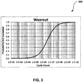
- FIG. 3 shows an exemplary CDF 300 illustrating the probability that a given block will exceed the correction power of a sector-level ECC due to wearout at some data age, in accordance with one embodiment.
- Sector level ECC may be utilized in flash to protect against soft errors and other effects. However, there is a finite limit to the power of the ECC, and this may be exceeded at some point due to block wearout. When this happens, corrupt data may be returned. Additional sector checks, such as a CRC, move the point at which this happens, but may not eliminate this issue.
- the curve in FIG. 3 is representative of what the actual field behavior may be at a short data age, in accordance with one embodiment. Assuming a device with an endurance specification of 10 5 cycles, this may be assigned to a 6% probability, given the JEDEC test results. In this example, it was assumed that 94% of the blocks fail at 10 8 cycles. At longer data ages, the curve would to shift to the left.
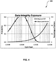
- FIG. 4 illustrates a representation 400 of the overlap between the access distribution and the CDF at some data age, showing the region of concern, in accordance with one embodiment.
- the overlap between the access distribution and the CDF may be seen.
- the narrower the access distribution the more likely a large percentage of blocks are in the wearout zone before the wearout is noticed. Thus, it is more likely that a power of the sector ECC will be exceeded and corrupt data will be returned.
- the error rate surface may be sampled to aid in the determination of the endurance and retention limits for a flash device. In one embodiment, this may be achieved by reserving a number of physical blocks that are not subject to wear leveling. These blocks may include data that is known to a host system such that the values may be fully verified, avoiding any aliasing problems inherent in using error rates determined from ECC.
- Such blocks may be used at an error rate beyond the ECC capabilities without compromising data integrity.
- the monitor data may also be verified at intervals to measure the error rate versus retention.
- a set of full erase blocks that are positioned near the expected rise of the CDF may be utilized to aid in determining wearout before it leads to data corruption.
- a flash device may have 16,000 erase blocks. Using 15 blocks as monitor data would take less than 0.1% of the device capacity.
- 15 blocks arranged in 5 groups of 3 may be utilized. Each group may have the same cycle count. In this case, having multiple blocks in a group may improve the quality of the measurement.
- the locations (in terms of cycle count) for each group may be chosen to be near the region where the CDF is expected to begin to have a magnitude that may impact data integrity.
- the time to erase/write/read a block is 138ms.
- a monitor data target layout of 5 monitor groups may be chosen.
- Table 2 shows a representation of a monitor data target layout of 5 monitor groups, in accordance with one embodiment.
- Table 2 Target Cycles (K) 20 36 63 112 200 Total Time to Deploy (H) 2.3 4.1 7.3 12.9 23.0 50
- the cycle counts are chosen to be power-law distributed assuming that wearout has a log-normal behavior. In various embodiments, other distributions may be chosen to maximize the effectiveness of the monitor data. In this example, it would take a total of 50 hours to cycle all the monitor data to the final counts.
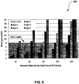
- FIG. 5 shows representative cycle count histograms 500 for a user and monitor data at some point in time, in accordance with one embodiment.
- the histograms of user data and monitor data are shown as function of write cycle count.
- the data includes wear leveling.
- the monitor data is positioned near the anticipated wearout cycle count.
- the time required to cycle all the monitor data blocks may be longer than desirable to perform prior to shipment.
- the monitor data may be partially cycled prior to shipment, with the remainder of the cycling occurring in the field.
- the blocks may be read at intervals and the read data may be compared with the known data. This allows complete identification of errors, including the ability to maintain a rate of change.
- FIG. 6 shows one possible set of measurements 600 from a monitor data system.
- Each monitor group is shown as a column group and each in the group represents a different data age.
- the height of each column is the number of errors per sector and the lower region labeled "ECC Limit" represents a possible ECC correction limit. As shown, some measurements may exceed the ECC capability and thus pose a risk for data integrity.
- operational limits may be derived from this data.
- Table 3 shows operational limits that may be generated for the exemplary data in FIG. 6 , in accordance with one embodiment.
- Table 3 Minimum Cycle Count Maximum Cycle Count Maximum Data Age ⁇ 40k 4 40k 60k 3 60k 80k 2 80k 100k 2 100k 120k 1 >120k Not allowed
- a monitoring data pattern may also be chosen. In various embodiments, this may be a static pattern or be computed for a particular block. As an option, a pattern that stresses the endurance and/or retention may be utilized. In either case, a system may be configured such that the expected contents of each monitor block may be known without reading anything from the flash device. When one of the limits is reached, the system may be informed by a S.M.A.R.T. flag, or another technique such as no longer accepting writes (e.g. returning error on write, etc.).
- the monitor data units may be as small as a sector size.
- FIG. 7 illustrates a method 700 for analyzing monitor data information from a plurality of flash memory devices, in accordance with one embodiment.
- monitor data information is gathered from a plurality of flash memory devices, the monitor data being data of known content stored in dedicated memory cells of known write cycle count. See operation 702.
- the monitor data may include any data or data pattern that is known.
- the monitor data information may include error rate information relating to at least one of the data age of the monitor data and the write cycle count.
- monitor data and/or the monitor data information may be gathered using a variety of techniques.
- the monitor data may be generated.
- the monitor data information is gathered, the monitor data information is analyzed. See operation 704. Additionally, an action is taken relating to at least one of the devices based on the analyzing. See operation 706.
- the action may include a variety of actions.
- taking the action may include setting a behavioral target for at least one of the devices.
- the behavioral target may be a limit on data write cycle count.
- the behavioral target may be a limit on data age.
- taking the action may include setting a behavioral target for at least one of the devices.
- the behavioral target may be a limit on data write cycle count.
- the behavioral target may be a limit on data age.
- the gathering of the monitor data information and the analyzing of the information may occur any number of times.
- the gathering and analyzing steps may be performed at least twice, and a statistical trend may be generated based thereon. Additionally, the gathering and analyzing steps may be performed at least twice, and a time-dependence of the monitor data may be tracked.
- the behavioral target may be updated after a period of time.
- monitor data may be gathered again and analyzed to generate an updated behavioral target after a period of time has elapsed from when a prior behavioral target was set. This will thus take into account the effect of the longer age of the monitor data, potentially improving the behavioral target.
- the behavioral target may be updated based at least in part on other factors such as failure events of memory devices, additional information or parameters that became available since the target was set, etc.
- the monitor data approach may be utilized to provide a measurement of the error rate surface in a set of flash devices in a storage system. Furthermore, a measure of the error rate vs. cycle count and error rate vs. data age may be provided for a given flash device.
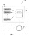
- FIG. 8 illustrates a representative storage system 800, in accordance with one embodiment.
- the storage system 800 may include a storage controller 802 and a plurality of flash devices 804.
- the behavior of the system 800 may be adjusted in response to monitor data information.
- the controller 802 may be in communication with a remote data repository 806 that aggregates field data from such storage systems.
- the controller 802 may determine likely initial cycle count targets for the set of local flash devices 804 based on this data, or as a factory preset. These values may be passed to the flash devices 804, which will cycle their monitor data to place it at the predetermined cycle counts. The storage controller 802 may then collect the error characteristics of the monitor data at different times.
- the storage controller 802 may include, or have access to, a real-time clock. This clock may be used to record the write times of the monitor data (either in the monitor data or in another reserved area) and to determine the age of the monitor data.
- the error characteristics reported by the monitor data may be collected over an interface to the flash device, such as via S.M.A.R.T.
- the storage system 800 may aggregate the collected data from the flash devices 804 to improve the statistics, and identify outliers.
- the storage system 800 may comprise 16 flash units (e.g. SSDs), each of which may comprise 16 flash devices. This provides 256 flash devices, thus improving the quality of the samples by 16x (assuming Poisson statistics). If each flash device had 3 blocks in each data set, the system data set size would be 768 block samples for each set. Thus, it is possible to obtain good statistics and to perform outlier detection.
- 16 flash units e.g. SSDs
- This provides 256 flash devices, thus improving the quality of the samples by 16x (assuming Poisson statistics). If each flash device had 3 blocks in each data set, the system data set size would be 768 block samples for each set. Thus, it is possible to obtain good statistics and to perform outlier detection.
- the monitor data may report the error configuration for each monitor data set. Each set may have a different cycle count. Thus, the storage controller 802 may use them to estimate the error rate curve for the population.
- the error rate curve may be used to select the endurance and retention limit criteria.
- a Monte Carlo simulation may be performed to generate a set of error count measurements for the monitor data on each device.
- the monitor data reports at least the mean error count for each monitor data block.
- the error count values for each cycle count are merged to compute the mean and standard deviation.
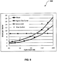
- the monitor data is sampled at 5 separate cycle counts.
- the "Mean” row lists the mean number of errors per sector, and the “Sigma” row lists the corresponding standard deviation.
- the "Sigma Clip Curve” row is the 4.8 standard deviation value at each cycle count. The last row is the number of devices which have error counts exceeding 4.8 standard deviations.
- FIG. 9 shows a graph 900 of the results, in accordance with this example.
- the graph 900 illustrates that the outlier is well beyond the edge of the distribution, and therefore applying the normal clip limit would likely result in an error exposure.
- the cycle count limits Once the cycle count limits have been computed, they may be fed back to the flash devices or a controller responsible for the endurance limits. This may be repeated at different times, thus reflecting different data ages. As such, a set of endurance and retention targets may both be generated for a storage system.
- Each monitor data set may include a plurality of erase blocks, each of which comprises many data sectors.
- a typical NAND device may have 528kB erase blocks, including 1024 sectors, each with 528 bytes. Assuming that each monitor set used 3 data blocks, for the entire set of 256 devices there are 3.3x10 9 bits per set. Thus, reliability is enhanced and costs are decreased since overkill is avoided.
- a system may include a flash memory device having a plurality of memory blocks, where at least one of the blocks has monitor data written therein, and the at least one block has been written to a plurality of times prior to writing the monitor data.
- the system may also include circuitry for addressing the blocks and a secondary memory storing a copy of the monitor data.
- the system may include a storage controller and a plurality of flash memory devices.
- the present invention may be embodied as a system, method or computer program product. Accordingly, the present invention may take the form of an entirely hardware embodiment, an entirely software embodiment (including firmware, resident software, micro-code, etc.) or an embodiment combining software and hardware aspects that may all generally be referred to herein as a "circuit,” "module” or “system.” Furthermore, the present invention may take the form of a computer program product embodied in any tangible medium of expression having computer-usable program code embodied in the medium.
- the computer-usable or computer-readable medium may be, for example but not limited to, an electronic, magnetic, optical, electromagnetic, infrared, or semiconductor system, apparatus, device, or propagation medium.
- the computer-readable medium would include the following: an electrical connection having one or more wires, a portable computer diskette, a hard disk, a random access memory (RAM), a read-only memory (ROM), an erasable programmable read-only memory (EPROM or Flash memory), an optical fiber, a portable compact disc read-only memory (CD-ROM), an optical storage device, a transmission media such as those supporting the Internet or an intranet, or a magnetic storage device.
- RAM random access memory
- ROM read-only memory
- EPROM or Flash memory erasable programmable read-only memory
- CD-ROM compact disc read-only memory
- CD-ROM compact disc read-only memory
- a transmission media such as those supporting the Internet or an intranet, or a magnetic storage device.
- a computer-usable or computer-readable medium could even be paper or another suitable medium upon which the program is printed, as the program can be electronically captured, via, for instance, optical scanning of the paper or other medium, then compiled, interpreted, or otherwise processed in a suitable manner, if necessary, and then stored in a computer memory.
- a computer-usable or computer-readable medium may be any medium that can contain, store, communicate, propagate, or transport the program for use by or in connection with the instruction execution system, apparatus, or device.
- the computer-usable medium may include a propagated data signal with the computer-usable program code embodied therewith, either in baseband or as part of a carrier wave.
- the computer usable program code may be transmitted using any appropriate medium, including but not limited to wireless, wireline, optical fiber cable, RF, etc.
- These computer program instructions may also be stored in a computer-readable medium that can direct a computer or other programmable data processing apparatus to function in a particular manner, such that the instructions stored in the computer-readable medium produce an article of manufacture including instruction means which implement the function/act specified in the flowchart and/or block diagram block or blocks.
- the computer program instructions may also be loaded onto a computer or other programmable data processing apparatus to cause a series of operational steps to be performed on the computer or other programmable apparatus to produce a computer implemented process such that the instructions which execute on the computer or other programmable apparatus provide processes for implementing the functions/acts specified in the flowchart and/or block diagram block or blocks.
- each block in the flowchart or block diagrams may represent a module, segment, or portion of code, which comprises one or more executable instructions for implementing the specified logical function(s).
- the functions noted in the block may occur out of the order noted in the figures. For example, two blocks shown in succession may, in fact, be executed substantially concurrently, or the blocks may sometimes be executed in the reverse order, depending upon the functionality involved.
- a data processing system suitable for storing and/or executing program code will include at least one processor coupled directly or indirectly to memory elements through a system bus.
- the memory elements can include local memory employed during actual execution of the program code, bulk storage, and cache memories which provide temporary storage of at least some program code in order to reduce the number of times code must be retrieved from bulk storage during execution.
- I/O devices including but not limited to keyboards, displays, pointing devices, etc.
- I/O controllers can be coupled to the system either directly or through intervening I/O controllers.
- Network adapters may also be coupled to the system to enable the data processing system to become coupled to other data processing systems or remote printers or storage devices through intervening private or public networks.
- Modems, cable modem and Ethernet cards are just a few of the currently available types of network adapters.
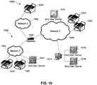
- FIG. 10 illustrates a network architecture 1000, in accordance with one embodiment.
- the functionality and architecture of FIGS. 1-9 may be implemented in the context of the network architecture 1000.
- the functionality and architecture of FIGS. 1-9 may be carried out in any desired environment. It should be noted that the aforementioned definitions may apply during the present description.
- a plurality of remote networks 1002 are provided including a first remote network 1004 and a second remote network 1006.
- a gateway 1007 may be coupled between the remote networks 1002 and a proximate network 1008.
- the networks 1004, 1006 may each take any form including, but not limited to a LAN, a WAN such as the Internet, PSTN, internal telephone network, etc.
- the gateway 1007 serves as an entrance point from the remote networks 1002 to the proximate network 1008.
- the gateway 1007 may function as a router, which is capable of directing a given packet of data that arrives at the gateway 1007, and a switch, which furnishes the actual path in and out of the gateway 1007 for a given packet.
- At least one data server 1014 coupled to the proximate network 1008, and which is accessible from the remote networks 1002 via the gateway 1007.
- the data server(s) 1014 may include any type of computing device/groupware. Coupled to each data server 1014 is a plurality of user devices 1016. Such user devices 1016 may include a desktop computer, lap-top computer, hand-held computer, printer or any other type of logic. It should be noted that a user device 1017 may also be directly coupled to any of the networks, in one embodiment.
- a facsimile machine 1020 or series of facsimile machines 1020 may be coupled to one or more of the networks 1004, 1006, 1008. It should be noted that databases and/or additional components may be utilized with, or integrated into, any type of network element coupled to the networks 1004, 1006, 1008. In the context of the present description, a network element may refer to any component of a network.
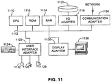
- FIG. 11 shows a representative hardware environment associated with a user device 1016 of FIG. 10 , in accordance with one embodiment.
- a user device 1016 of FIG. 10 Such figure illustrates a typical hardware configuration of a workstation having a central processing unit 1110, such as a microprocessor, and a number of other units interconnected via a system bus 1112.
- a central processing unit 1110 such as a microprocessor
- the workstation shown in FIG. 11 includes a Random Access Memory (RAM) 1114, Read Only Memory (ROM) 1116, an I/O adapter 1118 for connecting peripheral devices such as disk storage units 1120 to the bus 1112, a user interface adapter 1122 for connecting a keyboard 1124, a mouse 1126, a speaker 1128, a microphone 1132, and/or other user interface devices such as a touch screen and a digital camera (not shown) to the bus 1112, communication adapter 1134 for connecting the workstation to a communication network 1135 (e.g., a data processing network) and a display adapter 1136 for connecting the bus 1112 to a display device 1138.
- RAM Random Access Memory
- ROM Read Only Memory
- I/O adapter 1118 for connecting peripheral devices such as disk storage units 1120 to the bus 1112
- a user interface adapter 1122 for connecting a keyboard 1124, a mouse 1126, a speaker 1128, a microphone 1132, and/or other user interface devices such as a touch screen
- the workstation may have resident thereon an operating system such as the Microsoft Windows® Operating System (OS), a MAC OS, or UNIX operating system. It will be appreciated that a preferred embodiment may also be implemented on platforms and operating systems other than those mentioned.
- OS Microsoft Windows® Operating System
- a preferred embodiment may be written using JAVA, XML, C, and/or C++ language, or other programming languages, along with an object oriented programming methodology.
- Object oriented programming (OOP) which has become increasingly used to develop complex applications, may be used.
Applications Claiming Priority (2)
| Application Number | Priority Date | Filing Date | Title |
|---|---|---|---|
| US12/420,628 US8316173B2 (en) | 2009-04-08 | 2009-04-08 | System, method, and computer program product for analyzing monitor data information from a plurality of memory devices having finite endurance and/or retention |
| PCT/EP2010/053943 WO2010115726A2 (en) | 2009-04-08 | 2010-03-25 | Analyzing monitor data information from memory devices having finite endurance and/or retention |
Publications (2)
| Publication Number | Publication Date |
|---|---|
| EP2417603A2 EP2417603A2 (en) | 2012-02-15 |
| EP2417603B1 true EP2417603B1 (en) | 2018-04-25 |
Family
ID=42359564
Family Applications (1)
| Application Number | Title | Priority Date | Filing Date |
|---|---|---|---|
| EP10717562.2A Not-in-force EP2417603B1 (en) | 2009-04-08 | 2010-03-25 | Analyzing monitor data information from memory devices having finite endurance and/or retention |
Country Status (5)
| Country | Link |
|---|---|
| US (2) | US8316173B2 (ja) |
| EP (1) | EP2417603B1 (ja) |
| JP (1) | JP5596123B2 (ja) |
| CN (1) | CN102301427A (ja) |
| WO (1) | WO2010115726A2 (ja) |
Families Citing this family (54)
| Publication number | Priority date | Publication date | Assignee | Title |
|---|---|---|---|---|
| US8316173B2 (en) * | 2009-04-08 | 2012-11-20 | International Business Machines Corporation | System, method, and computer program product for analyzing monitor data information from a plurality of memory devices having finite endurance and/or retention |
| US8572443B2 (en) * | 2009-04-08 | 2013-10-29 | International Business Machines Corporation | System, method, and computer program product for determining a retention behavior for at least one block of a memory device having finite endurance and/or retention |
| US8909851B2 (en) | 2011-02-08 | 2014-12-09 | SMART Storage Systems, Inc. | Storage control system with change logging mechanism and method of operation thereof |
| US8935466B2 (en) | 2011-03-28 | 2015-01-13 | SMART Storage Systems, Inc. | Data storage system with non-volatile memory and method of operation thereof |
| US9135160B1 (en) | 2011-03-28 | 2015-09-15 | Rambus Inc. | Devices, systems, and methods for wear leveling memory |
| CN102163165B (zh) * | 2011-05-26 | 2012-11-14 | 忆正存储技术(武汉)有限公司 | 一种闪存错误预估模块及其预估方法 |
| US9098399B2 (en) | 2011-08-31 | 2015-08-04 | SMART Storage Systems, Inc. | Electronic system with storage management mechanism and method of operation thereof |
| US9063844B2 (en) | 2011-09-02 | 2015-06-23 | SMART Storage Systems, Inc. | Non-volatile memory management system with time measure mechanism and method of operation thereof |
| US9021231B2 (en) | 2011-09-02 | 2015-04-28 | SMART Storage Systems, Inc. | Storage control system with write amplification control mechanism and method of operation thereof |
| US9021319B2 (en) | 2011-09-02 | 2015-04-28 | SMART Storage Systems, Inc. | Non-volatile memory management system with load leveling and method of operation thereof |
| US10359949B2 (en) * | 2011-10-31 | 2019-07-23 | Apple Inc. | Systems and methods for obtaining and using nonvolatile memory health information |
| US8832506B2 (en) * | 2012-01-20 | 2014-09-09 | International Business Machines Corporation | Bit error rate based wear leveling for solid state drive memory |
| US9239781B2 (en) | 2012-02-07 | 2016-01-19 | SMART Storage Systems, Inc. | Storage control system with erase block mechanism and method of operation thereof |
| TWI455140B (zh) * | 2012-02-21 | 2014-10-01 | Fluiditech Ip Ltd | Flash memory usage period assessment method |
| US20130262942A1 (en) * | 2012-03-27 | 2013-10-03 | Yung-Chiang Chu | Flash memory lifetime evaluation method |
| US8996768B2 (en) | 2012-05-31 | 2015-03-31 | Sandisk Technologies Inc. | Method and storage device for assessing execution of trim commands |
| US8949689B2 (en) | 2012-06-11 | 2015-02-03 | SMART Storage Systems, Inc. | Storage control system with data management mechanism and method of operation thereof |
| US20130346812A1 (en) * | 2012-06-22 | 2013-12-26 | Micron Technology, Inc. | Wear leveling memory using error rate |
| US20150178193A1 (en) * | 2012-07-11 | 2015-06-25 | Industry-University Cooperation Foundation, Hanyang University | Apparatus and method for managing flash memory by means of writing data pattern recognition |
| US8856484B2 (en) * | 2012-08-14 | 2014-10-07 | Infinidat Ltd. | Mass storage system and methods of controlling resources thereof |
| US9671962B2 (en) | 2012-11-30 | 2017-06-06 | Sandisk Technologies Llc | Storage control system with data management mechanism of parity and method of operation thereof |
| US9123445B2 (en) | 2013-01-22 | 2015-09-01 | SMART Storage Systems, Inc. | Storage control system with data management mechanism and method of operation thereof |
| US9214965B2 (en) | 2013-02-20 | 2015-12-15 | Sandisk Enterprise Ip Llc | Method and system for improving data integrity in non-volatile storage |
| US9329928B2 (en) | 2013-02-20 | 2016-05-03 | Sandisk Enterprise IP LLC. | Bandwidth optimization in a non-volatile memory system |
| US9183137B2 (en) | 2013-02-27 | 2015-11-10 | SMART Storage Systems, Inc. | Storage control system with data management mechanism and method of operation thereof |
| US9470720B2 (en) | 2013-03-08 | 2016-10-18 | Sandisk Technologies Llc | Test system with localized heating and method of manufacture thereof |
| US9043780B2 (en) | 2013-03-27 | 2015-05-26 | SMART Storage Systems, Inc. | Electronic system with system modification control mechanism and method of operation thereof |
| US10049037B2 (en) | 2013-04-05 | 2018-08-14 | Sandisk Enterprise Ip Llc | Data management in a storage system |
| US9170941B2 (en) | 2013-04-05 | 2015-10-27 | Sandisk Enterprises IP LLC | Data hardening in a storage system |
| US9543025B2 (en) | 2013-04-11 | 2017-01-10 | Sandisk Technologies Llc | Storage control system with power-off time estimation mechanism and method of operation thereof |
| US10546648B2 (en) | 2013-04-12 | 2020-01-28 | Sandisk Technologies Llc | Storage control system with data management mechanism and method of operation thereof |
| US9313874B2 (en) | 2013-06-19 | 2016-04-12 | SMART Storage Systems, Inc. | Electronic system with heat extraction and method of manufacture thereof |
| US9898056B2 (en) | 2013-06-19 | 2018-02-20 | Sandisk Technologies Llc | Electronic assembly with thermal channel and method of manufacture thereof |
| US9244519B1 (en) | 2013-06-25 | 2016-01-26 | Smart Storage Systems. Inc. | Storage system with data transfer rate adjustment for power throttling |
| US9367353B1 (en) | 2013-06-25 | 2016-06-14 | Sandisk Technologies Inc. | Storage control system with power throttling mechanism and method of operation thereof |
| US9146850B2 (en) | 2013-08-01 | 2015-09-29 | SMART Storage Systems, Inc. | Data storage system with dynamic read threshold mechanism and method of operation thereof |
| US9448946B2 (en) | 2013-08-07 | 2016-09-20 | Sandisk Technologies Llc | Data storage system with stale data mechanism and method of operation thereof |
| US9431113B2 (en) | 2013-08-07 | 2016-08-30 | Sandisk Technologies Llc | Data storage system with dynamic erase block grouping mechanism and method of operation thereof |
| US9361222B2 (en) | 2013-08-07 | 2016-06-07 | SMART Storage Systems, Inc. | Electronic system with storage drive life estimation mechanism and method of operation thereof |
| US9152555B2 (en) | 2013-11-15 | 2015-10-06 | Sandisk Enterprise IP LLC. | Data management with modular erase in a data storage system |
| US10061638B2 (en) * | 2016-03-29 | 2018-08-28 | International Business Machines Corporation | Isolating faulty components in a clustered storage system with random redistribution of errors in data |
| CN107680632B (zh) * | 2016-08-01 | 2020-10-16 | 大唐移动通信设备有限公司 | 一种固态硬盘的寿命测试方法及装置 |
| US11947814B2 (en) | 2017-06-11 | 2024-04-02 | Pure Storage, Inc. | Optimizing resiliency group formation stability |
| CN108648778B (zh) * | 2018-05-21 | 2020-10-09 | 深圳忆联信息系统有限公司 | 一种固态硬盘读系统及其方法 |
| CN108845765B (zh) * | 2018-05-31 | 2021-06-29 | 郑州云海信息技术有限公司 | 一种nand数据读取方法、系统、设备及存储介质 |
| US10585625B2 (en) * | 2018-07-12 | 2020-03-10 | Micron Technology, Inc. | Determination of data integrity based on sentinel cells |
| US11354058B2 (en) * | 2018-09-06 | 2022-06-07 | Pure Storage, Inc. | Local relocation of data stored at a storage device of a storage system |
| US11520514B2 (en) | 2018-09-06 | 2022-12-06 | Pure Storage, Inc. | Optimized relocation of data based on data characteristics |
| US11500570B2 (en) | 2018-09-06 | 2022-11-15 | Pure Storage, Inc. | Efficient relocation of data utilizing different programming modes |
| US10564864B1 (en) * | 2018-10-04 | 2020-02-18 | Dell Products L.P. | Method for estimating data retention time in a solid state drive |
| US10963185B2 (en) | 2018-11-20 | 2021-03-30 | Micron Technology, Inc. | Memory sub-system for performing wear-leveling adjustments based on memory component endurance estimations |
| US11106370B2 (en) * | 2019-07-02 | 2021-08-31 | Micron Technology, Inc. | Changing of memory components to be used for a stripe based on an endurance condition |
| US11681448B2 (en) | 2020-09-08 | 2023-06-20 | Pure Storage, Inc. | Multiple device IDs in a multi-fabric module storage system |
| US11832410B2 (en) | 2021-09-14 | 2023-11-28 | Pure Storage, Inc. | Mechanical energy absorbing bracket apparatus |
Family Cites Families (19)
| Publication number | Priority date | Publication date | Assignee | Title |
|---|---|---|---|---|
| JPH03110650A (ja) * | 1989-09-25 | 1991-05-10 | Casio Comput Co Ltd | Eepromチェック方式 |
| JPH04328395A (ja) * | 1991-04-26 | 1992-11-17 | Fuji Electric Co Ltd | E2 romの書き込み回数オーバのチエック方法 |
| JP2001147862A (ja) * | 1999-11-22 | 2001-05-29 | Alps Electric Co Ltd | フラッシュメモリ書込方法 |
| US6829739B1 (en) * | 2000-08-10 | 2004-12-07 | Siemens Information And Communication Networks, Inc. | Apparatus and method for data buffering |
| US20040268190A1 (en) | 2003-05-19 | 2004-12-30 | International Business Machines Corporation | Adjusting parameters of a serial link |
| US7372731B2 (en) | 2003-06-17 | 2008-05-13 | Sandisk Il Ltd. | Flash memories with adaptive reference voltages |
| US7173852B2 (en) | 2003-10-03 | 2007-02-06 | Sandisk Corporation | Corrected data storage and handling methods |
| KR100704618B1 (ko) * | 2004-01-19 | 2007-04-10 | 삼성전자주식회사 | 플래시 메모리의 데이터 복구 장치 및 방법 |
| US20060026467A1 (en) | 2004-07-30 | 2006-02-02 | Smadar Nehab | Method and apparatus for automatically discovering of application errors as a predictive metric for the functional health of enterprise applications |
| US7409623B2 (en) * | 2004-11-04 | 2008-08-05 | Sigmatel, Inc. | System and method of reading non-volatile computer memory |
| JP4863749B2 (ja) | 2006-03-29 | 2012-01-25 | 株式会社日立製作所 | フラッシュメモリを用いた記憶装置、その消去回数平準化方法、及び消去回数平準化プログラム |
| US7778077B2 (en) * | 2006-05-15 | 2010-08-17 | Sandisk Corporation | Non-volatile memory system with end of life calculation |
| US7523013B2 (en) * | 2006-05-15 | 2009-04-21 | Sandisk Corporation | Methods of end of life calculation for non-volatile memories |
| US7558109B2 (en) | 2006-11-03 | 2009-07-07 | Sandisk Corporation | Nonvolatile memory with variable read threshold |
| US20080140918A1 (en) | 2006-12-11 | 2008-06-12 | Pantas Sutardja | Hybrid non-volatile solid state memory system |
| US7962792B2 (en) * | 2008-02-11 | 2011-06-14 | Siliconsystems, Inc. | Interface for enabling a host computer to retrieve device monitor data from a solid state storage subsystem |
| US8380946B2 (en) * | 2009-04-08 | 2013-02-19 | International Business Machines Corporation | System, method, and computer program product for estimating when a reliable life of a memory device having finite endurance and/or retention, or portion thereof, will be expended |
| US8572443B2 (en) * | 2009-04-08 | 2013-10-29 | International Business Machines Corporation | System, method, and computer program product for determining a retention behavior for at least one block of a memory device having finite endurance and/or retention |
| US8316173B2 (en) | 2009-04-08 | 2012-11-20 | International Business Machines Corporation | System, method, and computer program product for analyzing monitor data information from a plurality of memory devices having finite endurance and/or retention |
-
2009
- 2009-04-08 US US12/420,628 patent/US8316173B2/en active Active
-
2010
- 2010-03-25 EP EP10717562.2A patent/EP2417603B1/en not_active Not-in-force
- 2010-03-25 CN CN201080005997XA patent/CN102301427A/zh active Pending
- 2010-03-25 JP JP2012503953A patent/JP5596123B2/ja not_active Expired - Fee Related
- 2010-03-25 WO PCT/EP2010/053943 patent/WO2010115726A2/en active Application Filing
-
2012
- 2012-09-14 US US13/617,996 patent/US8554989B2/en active Active
Non-Patent Citations (1)
| Title |
|---|
| None * |
Also Published As
| Publication number | Publication date |
|---|---|
| US8554989B2 (en) | 2013-10-08 |
| WO2010115726A2 (en) | 2010-10-14 |
| US20130013968A1 (en) | 2013-01-10 |
| EP2417603A2 (en) | 2012-02-15 |
| JP5596123B2 (ja) | 2014-09-24 |
| US20100262795A1 (en) | 2010-10-14 |
| CN102301427A (zh) | 2011-12-28 |
| US8316173B2 (en) | 2012-11-20 |
| JP2012523599A (ja) | 2012-10-04 |
| WO2010115726A3 (en) | 2010-12-23 |
Similar Documents
| Publication | Publication Date | Title |
|---|---|---|
| EP2417603B1 (en) | Analyzing monitor data information from memory devices having finite endurance and/or retention | |
| US8380946B2 (en) | System, method, and computer program product for estimating when a reliable life of a memory device having finite endurance and/or retention, or portion thereof, will be expended | |
| US8572443B2 (en) | System, method, and computer program product for determining a retention behavior for at least one block of a memory device having finite endurance and/or retention | |
| US10963327B2 (en) | Detecting error count deviations for non-volatile memory blocks for advanced non-volatile memory block management | |
| Mielke et al. | Reliability of solid-state drives based on NAND flash memory | |
| US8650446B2 (en) | Management of a non-volatile memory based on test quality | |
| US20210182166A1 (en) | Zoned namespace management of non-volatile storage devices | |
| US20170131948A1 (en) | Visualization of usage impacts on solid state drive life acceleration | |
| US8910002B2 (en) | NAND flash-based storage device with built-in test-ahead for failure anticipation | |
| US8122185B2 (en) | Systems and methods for measuring the useful life of solid-state storage devices | |
| US20170131947A1 (en) | Data and collection methods to analyze life acceleration of SSD with real usages | |
| US7992061B2 (en) | Method for testing reliability of solid-state storage medium | |
| US8645776B2 (en) | Run-time testing of memory locations in a non-volatile memory | |
| US20140136883A1 (en) | Read disturb effect determination | |
| JP5956675B2 (ja) | 記憶装置および記憶装置制御方法 | |
| US20120260138A1 (en) | Error logging in a storage device | |
| Pletka et al. | Management of next-generation NAND flash to achieve enterprise-level endurance and latency targets | |
| US10656847B2 (en) | Mitigating asymmetric transient errors in non-volatile memory by proactive data relocation | |
| CN107808686B (zh) | 读出错测试方法与装置 | |
| US11599403B2 (en) | Logging mechanism for memory system | |
| US10942662B2 (en) | Relocating and/or re-programming blocks of storage space based on calibration frequency and resource utilization | |
| Liu et al. | Research and Implementation of SSD Lifespan Protection Mechanism |
Legal Events
| Date | Code | Title | Description |
|---|---|---|---|
| PUAI | Public reference made under article 153(3) epc to a published international application that has entered the european phase |
Free format text: ORIGINAL CODE: 0009012 |
|
| 17P | Request for examination filed |
Effective date: 20111027 |
|
| AK | Designated contracting states |
Kind code of ref document: A2 Designated state(s): AT BE BG CH CY CZ DE DK EE ES FI FR GB GR HR HU IE IS IT LI LT LU LV MC MK MT NL NO PL PT RO SE SI SK SM TR |
|
| DAX | Request for extension of the european patent (deleted) | ||
| 17Q | First examination report despatched |
Effective date: 20131024 |
|
| GRAP | Despatch of communication of intention to grant a patent |
Free format text: ORIGINAL CODE: EPIDOSNIGR1 |
|
| STAA | Information on the status of an ep patent application or granted ep patent |
Free format text: STATUS: GRANT OF PATENT IS INTENDED |
|
| INTG | Intention to grant announced |
Effective date: 20171206 |
|
| GRAS | Grant fee paid |
Free format text: ORIGINAL CODE: EPIDOSNIGR3 |
|
| GRAA | (expected) grant |
Free format text: ORIGINAL CODE: 0009210 |
|
| STAA | Information on the status of an ep patent application or granted ep patent |
Free format text: STATUS: THE PATENT HAS BEEN GRANTED |
|
| AK | Designated contracting states |
Kind code of ref document: B1 Designated state(s): AT BE BG CH CY CZ DE DK EE ES FI FR GB GR HR HU IE IS IT LI LT LU LV MC MK MT NL NO PL PT RO SE SI SK SM TR |
|
| REG | Reference to a national code |
Ref country code: GB Ref legal event code: FG4D |
|
| REG | Reference to a national code |
Ref country code: CH Ref legal event code: EP |
|
| REG | Reference to a national code |
Ref country code: AT Ref legal event code: REF Ref document number: 993707 Country of ref document: AT Kind code of ref document: T Effective date: 20180515 |
|
| REG | Reference to a national code |
Ref country code: IE Ref legal event code: FG4D |
|
| REG | Reference to a national code |
Ref country code: DE Ref legal event code: R096 Ref document number: 602010050177 Country of ref document: DE |
|
| REG | Reference to a national code |
Ref country code: NL Ref legal event code: MP Effective date: 20180425 |
|
| REG | Reference to a national code |
Ref country code: LT Ref legal event code: MG4D |
|
| PG25 | Lapsed in a contracting state [announced via postgrant information from national office to epo] |
Ref country code: NL Free format text: LAPSE BECAUSE OF FAILURE TO SUBMIT A TRANSLATION OF THE DESCRIPTION OR TO PAY THE FEE WITHIN THE PRESCRIBED TIME-LIMIT Effective date: 20180425 |
|
| PG25 | Lapsed in a contracting state [announced via postgrant information from national office to epo] |
Ref country code: FI Free format text: LAPSE BECAUSE OF FAILURE TO SUBMIT A TRANSLATION OF THE DESCRIPTION OR TO PAY THE FEE WITHIN THE PRESCRIBED TIME-LIMIT Effective date: 20180425 Ref country code: BG Free format text: LAPSE BECAUSE OF FAILURE TO SUBMIT A TRANSLATION OF THE DESCRIPTION OR TO PAY THE FEE WITHIN THE PRESCRIBED TIME-LIMIT Effective date: 20180725 Ref country code: SE Free format text: LAPSE BECAUSE OF FAILURE TO SUBMIT A TRANSLATION OF THE DESCRIPTION OR TO PAY THE FEE WITHIN THE PRESCRIBED TIME-LIMIT Effective date: 20180425 Ref country code: NO Free format text: LAPSE BECAUSE OF FAILURE TO SUBMIT A TRANSLATION OF THE DESCRIPTION OR TO PAY THE FEE WITHIN THE PRESCRIBED TIME-LIMIT Effective date: 20180725 Ref country code: ES Free format text: LAPSE BECAUSE OF FAILURE TO SUBMIT A TRANSLATION OF THE DESCRIPTION OR TO PAY THE FEE WITHIN THE PRESCRIBED TIME-LIMIT Effective date: 20180425 Ref country code: LT Free format text: LAPSE BECAUSE OF FAILURE TO SUBMIT A TRANSLATION OF THE DESCRIPTION OR TO PAY THE FEE WITHIN THE PRESCRIBED TIME-LIMIT Effective date: 20180425 Ref country code: PL Free format text: LAPSE BECAUSE OF FAILURE TO SUBMIT A TRANSLATION OF THE DESCRIPTION OR TO PAY THE FEE WITHIN THE PRESCRIBED TIME-LIMIT Effective date: 20180425 |
|
| PG25 | Lapsed in a contracting state [announced via postgrant information from national office to epo] |
Ref country code: HR Free format text: LAPSE BECAUSE OF FAILURE TO SUBMIT A TRANSLATION OF THE DESCRIPTION OR TO PAY THE FEE WITHIN THE PRESCRIBED TIME-LIMIT Effective date: 20180425 Ref country code: LV Free format text: LAPSE BECAUSE OF FAILURE TO SUBMIT A TRANSLATION OF THE DESCRIPTION OR TO PAY THE FEE WITHIN THE PRESCRIBED TIME-LIMIT Effective date: 20180425 Ref country code: GR Free format text: LAPSE BECAUSE OF FAILURE TO SUBMIT A TRANSLATION OF THE DESCRIPTION OR TO PAY THE FEE WITHIN THE PRESCRIBED TIME-LIMIT Effective date: 20180726 |
|
| REG | Reference to a national code |
Ref country code: AT Ref legal event code: MK05 Ref document number: 993707 Country of ref document: AT Kind code of ref document: T Effective date: 20180425 |
|
| PG25 | Lapsed in a contracting state [announced via postgrant information from national office to epo] |
Ref country code: PT Free format text: LAPSE BECAUSE OF FAILURE TO SUBMIT A TRANSLATION OF THE DESCRIPTION OR TO PAY THE FEE WITHIN THE PRESCRIBED TIME-LIMIT Effective date: 20180827 |
|
| REG | Reference to a national code |
Ref country code: DE Ref legal event code: R097 Ref document number: 602010050177 Country of ref document: DE |
|
| PG25 | Lapsed in a contracting state [announced via postgrant information from national office to epo] |
Ref country code: EE Free format text: LAPSE BECAUSE OF FAILURE TO SUBMIT A TRANSLATION OF THE DESCRIPTION OR TO PAY THE FEE WITHIN THE PRESCRIBED TIME-LIMIT Effective date: 20180425 Ref country code: CZ Free format text: LAPSE BECAUSE OF FAILURE TO SUBMIT A TRANSLATION OF THE DESCRIPTION OR TO PAY THE FEE WITHIN THE PRESCRIBED TIME-LIMIT Effective date: 20180425 Ref country code: RO Free format text: LAPSE BECAUSE OF FAILURE TO SUBMIT A TRANSLATION OF THE DESCRIPTION OR TO PAY THE FEE WITHIN THE PRESCRIBED TIME-LIMIT Effective date: 20180425 Ref country code: AT Free format text: LAPSE BECAUSE OF FAILURE TO SUBMIT A TRANSLATION OF THE DESCRIPTION OR TO PAY THE FEE WITHIN THE PRESCRIBED TIME-LIMIT Effective date: 20180425 Ref country code: DK Free format text: LAPSE BECAUSE OF FAILURE TO SUBMIT A TRANSLATION OF THE DESCRIPTION OR TO PAY THE FEE WITHIN THE PRESCRIBED TIME-LIMIT Effective date: 20180425 Ref country code: SK Free format text: LAPSE BECAUSE OF FAILURE TO SUBMIT A TRANSLATION OF THE DESCRIPTION OR TO PAY THE FEE WITHIN THE PRESCRIBED TIME-LIMIT Effective date: 20180425 |
|
| PG25 | Lapsed in a contracting state [announced via postgrant information from national office to epo] |
Ref country code: SM Free format text: LAPSE BECAUSE OF FAILURE TO SUBMIT A TRANSLATION OF THE DESCRIPTION OR TO PAY THE FEE WITHIN THE PRESCRIBED TIME-LIMIT Effective date: 20180425 Ref country code: IT Free format text: LAPSE BECAUSE OF FAILURE TO SUBMIT A TRANSLATION OF THE DESCRIPTION OR TO PAY THE FEE WITHIN THE PRESCRIBED TIME-LIMIT Effective date: 20180425 |
|
| PLBE | No opposition filed within time limit |
Free format text: ORIGINAL CODE: 0009261 |
|
| STAA | Information on the status of an ep patent application or granted ep patent |
Free format text: STATUS: NO OPPOSITION FILED WITHIN TIME LIMIT |
|
| 26N | No opposition filed |
Effective date: 20190128 |
|
| PGFP | Annual fee paid to national office [announced via postgrant information from national office to epo] |
Ref country code: DE Payment date: 20190312 Year of fee payment: 10 |
|
| PG25 | Lapsed in a contracting state [announced via postgrant information from national office to epo] |
Ref country code: SI Free format text: LAPSE BECAUSE OF FAILURE TO SUBMIT A TRANSLATION OF THE DESCRIPTION OR TO PAY THE FEE WITHIN THE PRESCRIBED TIME-LIMIT Effective date: 20180425 |
|
| PG25 | Lapsed in a contracting state [announced via postgrant information from national office to epo] |
Ref country code: MC Free format text: LAPSE BECAUSE OF FAILURE TO SUBMIT A TRANSLATION OF THE DESCRIPTION OR TO PAY THE FEE WITHIN THE PRESCRIBED TIME-LIMIT Effective date: 20180425 |
|
| REG | Reference to a national code |
Ref country code: CH Ref legal event code: PL |
|
| GBPC | Gb: european patent ceased through non-payment of renewal fee |
Effective date: 20190325 |
|
| PG25 | Lapsed in a contracting state [announced via postgrant information from national office to epo] |
Ref country code: LU Free format text: LAPSE BECAUSE OF NON-PAYMENT OF DUE FEES Effective date: 20190325 |
|
| REG | Reference to a national code |
Ref country code: BE Ref legal event code: MM Effective date: 20190331 |
|
| PG25 | Lapsed in a contracting state [announced via postgrant information from national office to epo] |
Ref country code: GB Free format text: LAPSE BECAUSE OF NON-PAYMENT OF DUE FEES Effective date: 20190325 Ref country code: CH Free format text: LAPSE BECAUSE OF NON-PAYMENT OF DUE FEES Effective date: 20190331 Ref country code: LI Free format text: LAPSE BECAUSE OF NON-PAYMENT OF DUE FEES Effective date: 20190331 Ref country code: IE Free format text: LAPSE BECAUSE OF NON-PAYMENT OF DUE FEES Effective date: 20190325 |
|
| PG25 | Lapsed in a contracting state [announced via postgrant information from national office to epo] |
Ref country code: FR Free format text: LAPSE BECAUSE OF NON-PAYMENT OF DUE FEES Effective date: 20190331 Ref country code: BE Free format text: LAPSE BECAUSE OF NON-PAYMENT OF DUE FEES Effective date: 20190331 |
|
| PG25 | Lapsed in a contracting state [announced via postgrant information from national office to epo] |
Ref country code: TR Free format text: LAPSE BECAUSE OF FAILURE TO SUBMIT A TRANSLATION OF THE DESCRIPTION OR TO PAY THE FEE WITHIN THE PRESCRIBED TIME-LIMIT Effective date: 20180425 |
|
| PG25 | Lapsed in a contracting state [announced via postgrant information from national office to epo] |
Ref country code: MT Free format text: LAPSE BECAUSE OF NON-PAYMENT OF DUE FEES Effective date: 20190325 |
|
| REG | Reference to a national code |
Ref country code: DE Ref legal event code: R119 Ref document number: 602010050177 Country of ref document: DE |
|
| PG25 | Lapsed in a contracting state [announced via postgrant information from national office to epo] |
Ref country code: DE Free format text: LAPSE BECAUSE OF NON-PAYMENT OF DUE FEES Effective date: 20201001 |
|
| PG25 | Lapsed in a contracting state [announced via postgrant information from national office to epo] |
Ref country code: CY Free format text: LAPSE BECAUSE OF FAILURE TO SUBMIT A TRANSLATION OF THE DESCRIPTION OR TO PAY THE FEE WITHIN THE PRESCRIBED TIME-LIMIT Effective date: 20180425 |
|
| PG25 | Lapsed in a contracting state [announced via postgrant information from national office to epo] |
Ref country code: IS Free format text: LAPSE BECAUSE OF FAILURE TO SUBMIT A TRANSLATION OF THE DESCRIPTION OR TO PAY THE FEE WITHIN THE PRESCRIBED TIME-LIMIT Effective date: 20180825 |
|
| PG25 | Lapsed in a contracting state [announced via postgrant information from national office to epo] |
Ref country code: HU Free format text: LAPSE BECAUSE OF FAILURE TO SUBMIT A TRANSLATION OF THE DESCRIPTION OR TO PAY THE FEE WITHIN THE PRESCRIBED TIME-LIMIT; INVALID AB INITIO Effective date: 20100325 |
|
| PG25 | Lapsed in a contracting state [announced via postgrant information from national office to epo] |
Ref country code: MK Free format text: LAPSE BECAUSE OF FAILURE TO SUBMIT A TRANSLATION OF THE DESCRIPTION OR TO PAY THE FEE WITHIN THE PRESCRIBED TIME-LIMIT Effective date: 20180425 |
|
| P01 | Opt-out of the competence of the unified patent court (upc) registered |
Effective date: 20230413 |