EP2416626A2 - Circuit d'éclairage à source lumineuse et système de phare pour véhicule - Google Patents
Circuit d'éclairage à source lumineuse et système de phare pour véhicule Download PDFInfo
- Publication number
- EP2416626A2 EP2416626A2 EP11176694A EP11176694A EP2416626A2 EP 2416626 A2 EP2416626 A2 EP 2416626A2 EP 11176694 A EP11176694 A EP 11176694A EP 11176694 A EP11176694 A EP 11176694A EP 2416626 A2 EP2416626 A2 EP 2416626A2
- Authority
- EP
- European Patent Office
- Prior art keywords
- terminal
- current
- control terminal
- resistor
- light source
- Prior art date
- Legal status (The legal status is an assumption and is not a legal conclusion. Google has not performed a legal analysis and makes no representation as to the accuracy of the status listed.)
- Granted
Links
- 230000002265 prevention Effects 0.000 claims abstract description 28
- 230000003071 parasitic effect Effects 0.000 description 6
- 238000010586 diagram Methods 0.000 description 3
- 239000003990 capacitor Substances 0.000 description 2
- 230000020169 heat generation Effects 0.000 description 1
Images


Classifications
-
- H—ELECTRICITY
- H05—ELECTRIC TECHNIQUES NOT OTHERWISE PROVIDED FOR
- H05B—ELECTRIC HEATING; ELECTRIC LIGHT SOURCES NOT OTHERWISE PROVIDED FOR; CIRCUIT ARRANGEMENTS FOR ELECTRIC LIGHT SOURCES, IN GENERAL
- H05B45/00—Circuit arrangements for operating light-emitting diodes [LED]
- H05B45/30—Driver circuits
- H05B45/37—Converter circuits
- H05B45/3725—Switched mode power supply [SMPS]
- H05B45/38—Switched mode power supply [SMPS] using boost topology
-
- H—ELECTRICITY
- H05—ELECTRIC TECHNIQUES NOT OTHERWISE PROVIDED FOR
- H05B—ELECTRIC HEATING; ELECTRIC LIGHT SOURCES NOT OTHERWISE PROVIDED FOR; CIRCUIT ARRANGEMENTS FOR ELECTRIC LIGHT SOURCES, IN GENERAL
- H05B45/00—Circuit arrangements for operating light-emitting diodes [LED]
- H05B45/30—Driver circuits
- H05B45/345—Current stabilisation; Maintaining constant current
-
- Y—GENERAL TAGGING OF NEW TECHNOLOGICAL DEVELOPMENTS; GENERAL TAGGING OF CROSS-SECTIONAL TECHNOLOGIES SPANNING OVER SEVERAL SECTIONS OF THE IPC; TECHNICAL SUBJECTS COVERED BY FORMER USPC CROSS-REFERENCE ART COLLECTIONS [XRACs] AND DIGESTS
- Y02—TECHNOLOGIES OR APPLICATIONS FOR MITIGATION OR ADAPTATION AGAINST CLIMATE CHANGE
- Y02B—CLIMATE CHANGE MITIGATION TECHNOLOGIES RELATED TO BUILDINGS, e.g. HOUSING, HOUSE APPLIANCES OR RELATED END-USER APPLICATIONS
- Y02B20/00—Energy efficient lighting technologies, e.g. halogen lamps or gas discharge lamps
- Y02B20/30—Semiconductor lamps, e.g. solid state lamps [SSL] light emitting diodes [LED] or organic LED [OLED]
Definitions
- the present disclosure relates to a lighting circuit for a light source that lights the light source, and a lamp system for a vehicle.
- a lighting circuit for a light source (“a light source lighting eircuit”) has been known including a first circuit (e.g., a circuit for a stop lamp) that supplies a first driving current (e.g ., a constant current) to a light source and a second circuit (e.g. , a circuit for a tail lamp) that supplies a second driving current (e.g ., a constant current) smaller than the first driving current to the light source ( see, e.g., JP 2005-029020 A ).
- a first circuit e.g., a circuit for a stop lamp
- a second circuit e.g., a circuit for a tail lamp
- a first diode is connected between the first circuit and the light source, and a second diode is also connected between the second circuit and the light source.
- the first driving current is supplied to the light source from the first circuit by driving only the first circuit.
- the second driving current is supplied to the light source from the second circuit by driving only the second circuit.
- the first driving current is larger than the second driving current, so that the first diode needs to have a large maximum rated voltage and thus, an expensive diode is required to be used as the first diode. As a result, the cost of the light source lighting circuit and the lamp system for a vehicle including the same is increased.
- the present disclosure has been made to reduce product costs and circuit loss while maintaining a function to prevent a countercurrent.
- a lighting circuit for a light source.
- the lighting circuit comprises: a countercurrent prevention unit comprising a first control terminal and a second control terminal, the countercurrent prevention unit configured to transmit a first current or a second current that is smaller than the first current to the light source; and a current controller comprising: a common terminal connected to the first control terminal and the second control terminal; and a switching terminal connected to the first control terminal, the current controller configured to provide a first driving current or a second driving current from the common terminal to the light source, wherein the first driving current corresponds to the first current, and the second driving current corresponds to the second current.
- the countercurrent prevention unit further comprises: a first rectifier, wherein voltage at the first control terminal is provided to the switching terminal through the first rectifier; a first P-FET provided between the first control terminal and the common terminal; a second P-FET provided between the second control terminal and the common terminal; and a second rectifier provided between the second P-PET and the common terminal, wherein the second rectifier is series-connected to the second P-PET.
- a first rectifier wherein voltage at the first control terminal is provided to the switching terminal through the first rectifier
- a first P-FET provided between the first control terminal and the common terminal
- a second P-FET provided between the second control terminal and the common terminal
- the second rectifier provided between the second P-PET and the common terminal
- the exemplary embodiment of the present disclosure uses a P channel FET ("P-FET") with a low on-resistance having the countercurrent prevention function, such that the product costs of the light source lighting circuit and the lamp system for a vehicle including the same may be reduced, the power consumption of the circuit may be reduced, and it is ensured that the countercurrent caused by the reverse connection of the battery may be prevented, as compared with the case of using a diode.
- P-FET P channel FET
- the light source lighting circuit is, for example, a circuit for lighting a plurality of light sources mounted in a lamp system for a vehicle.
- a light source as, for example, a daytime running lamp and a position lamp.
- the light source serves as the daytime running lamp
- the position lamp when a command to light the position lamp is issued from the countercurrent prevention unit, the light source serves as the position lamp.
- the light source when a command to light both of the daytime running lamp and the position lamp is issued, the light source serves as the daytime running lamp.
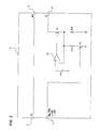
- a light source lighting circuit 1 includes a countercurrent prevention unit 2 having a first control terminal 4 and a second control terminal 5, and a current controller 3 having a common terminal 6 and a switching terminal 7.
- the countercurrent prevention unit 2 includes a first P-FET ("PMOS Trl”), a second P-FET ("PMOS Tr2”), and NPN transistors Tr3 and Tr4 ("NPN Tr3", “NPN Tr4") (a switch driving circuit).
- the countercurrent prevention unit 2 provides voltage from the first control terminal 4 to the switching terminal 7 through a diode D1 (a first rectifier).
- the countercurrent prevention unit 2 provides voltage from the second control terminal 5 to the common terminal 6 through a diode D2 (a second rectifier).
- the PMOS Tr1 has a drain connected to the first control terminal 4, a source connected to the common terminal 6, and a gate connected to a drain of the PMOS Tr2 through a resistor R1 and a diode D4 (a third rectifier).
- a parasitic diode D3 is present between the source and the drain.
- the Resistor R1 has one end connected to the gate of the PMOS Tr1 through a first connection point N1 and the other end connected to a second connection point N2 of the PMOS Tr2 and the diode D2 (a second rectifier).
- a resistor R2 (a second resistor) has one end connected to the gate of the PMOS Tr1 and one end of the resistor R1 through the first connection point N1 and the other end connected to the ground.
- the resistance value of the resistor R2 is larger than that of the resistor R1.
- a potential difference generating element (a zener diode or resistor) may be connected between the first connection point N1 and the source of the PMOS Tr1.
- the PMOS Tr2 has a drain connected to the common terminal 6 through the diode D2, a source connected to the second control terminal 5, and a gate connected to the collector of the NPN Tr3 through a diode D5 and a resistor R4.
- a parasitic diode D6 is present between the source and the drain.
- the PMOS Tr2 and diode D2 are connected to each other in series.
- the NPN Tr3 has an emitter connected to the ground and a base connected to a collector of the NPN Tr4 through a resistor R6.
- a resistor R7 is connected between the base and the emitter.
- the NPN Tr4 has an emitter connected to a ground, a base connected to first control terminal 4 through a resistor R8 and diode D1, and a collector connected to the second control terminal 5 and the source of the PMOS Tr2 through a resistor R5 and a diode D7.
- a resistor R9 is connected between the base and the emitter.
- the current controller 3 includes the common terminal 6, the switching terminal 7, an output terminal 8, and an input terminal 9, and supplies a driving current through the output terminal 8 to light emitting diodes (LEDs) 40, 40, and 40 connected in series as a light source.
- LEDs light emitting diodes
- the driving current that lights the daytime running lamp is referred to as a first driving current 11 (a corresponding current to the first current), and the driving current that lights the position lamp is referred to as a second driving current 12 (a corresponding current to the second current).
- a constant current clamp circuit including an operational amplifier and an NMOS transistor at the cathode sides of the LEDs 40, 40, and 40 may be used (see, e.g., FIG. 2 ).
- the constant current clamp circuit has a function that feeds back the driving voltage corresponding to the driving current of the LEDs 40, 40, and 40 to stably control the driving current, so that the driving voltage becomes a preset reference voltage.
- the constant current clamp circuit is configured to include an operational amplifier 13, NMOS Tr5 and NMOS Tr6, and resistor R12 and resistor R13.
- the switching terminal 7 is connected to a gate of the NMOS Tr6.
- the NMOS Tr6 has a drain connected to an inverting input terminal of operational amplifier 13 through a resistor R13 and a source connected to the ground.
- a predetermined reference voltage Vref is provided to a non-inverting input terminal of the operational amplifier 13.
- the output from the operational amplifier 13 is provided to a gate of the NMOS Tr5.
- the NMOS Tr5 has a drain connected to the input terminal 9 and a source connected to one end of each of the resistors R12 and R13.
- a switching regulator circuit including a PWM comparator, an error amplifier, and an NMOS transistor may be used (see, e.g., FIG. 3 ).
- the switching regulator circuit feeds back the first driving voltage or the second driving voltage corresponding to the first driving current I1 or the second driving current 12 that is supplied to LEDs 40, 40, and 40, respectively, to switch the switching element at a high speed so that the first driving voltage or the second driving voltage becomes a preset reference voltage, and to change the duty ratio of on/off of the switching element.
- the switching regulator circuit serves to stably control the first driving current I1 or the second driving current 12 supplied to the LEDs 40, 40, and 40.
- the switching regulator circuit includes capacitors C1 and C2, a choke coil L, NMOS Tr7 and Tr8, a PWM comparator 22, an error amplifier 23, and resistors R14 and R15.
- the common terminal 6 is connected to the capacitor C 1 and the choke coil L.
- the first driving current I1 or the second driving current 12 from the common terminal 6 is supplied to the output terminal 8 through the choke coil L and the diode D8.
- the switching terminal 7 is connected to a gate of the NMOS Tr7.
- the NMOS Tr7 includes a drain connected an inverting input terminal and the input terminal 9 of the error amplifier 23 through the resistor R15, and a source connected to the ground.
- the input terminal 9 is connected to one end of each of the resistor R14 and the resistor R15.
- a predetermined reference voltage Vref is provided to the non-inverting input terminal of the error amplifier 23.
- the output from the error amplifier 23 is provided to the PWM comparator 22.
- the output from the PWM comparator 22 is provided to the gate of the NMOS transistor Tr8.
- the NMOS Tr8 includes a drain connected to the choke coil L and the diode D8, and a source connected to the ground.
- a switch SW1 and a switch SW2 each having an on/off function are connected between the countercurrent prevention unit 2 and the battery (a DC power supply (+ B)) (see, e.g. , FIG. 1 ).
- the DC power voltage is transmitted to the first control terminal 4 to supply the first driving current I1 to the LEDs 40, 40, and 40.
- the switch SW2 is turned-on, the DC power voltage is transmitted to the second control terminal 5 to cause the first driving current 12 to be supplied to the LEDs 40, 40, and 40.
- the switch SW1 and the switch SW2 are simultaneously turned-on, the DC power voltage is transmitted to the first control terminal 4 and the second control terminal 5 to cause the first driving current I1 to be supplied to the LEDs 40, 40, and 40.
- a plurality of earth terminals is disposed in the light source lighting circuit 1. and all of the earth terminals are electrically connected.
- the DC power voltage (+B) is provided to the first control terminal 4 but not to the second control terminal 5, and the DC power voltage (e.g. , a control signal) is transmitted to the parasitic diode D3 and the base of the NPN Tr4 through the first control terminal 4.
- the output from the switching terminal 7 is in a high level, such that a first current is supplied to the common terminal 6.
- the NPN Tr4 is turned-on by receiving the DC power voltage (e.g., a control signal) through the diode D1.
- the NPN Tr4 is turned-on, the NPN Tr3 is turned-off. Therefore, since the potential difference is not generated in resistor R3 and the gate-source voltage of the PMOS Tr2 is not generated, the PMOS transistor Tr2 is turned-off. Therefore, voltage is not applied to the gate of the PMOS Tr1 and thus the PMOS Tr1 is maintained in a turn-on state. Therefore, the first driving current I1 is transmitted to the common terminal 6 through the PMOS Tr1.
- the DC power voltage is provided to the switching terminal 7 through the diode D1.
- the operation of the current controller 3 after the DC power voltage is provided to the switching terminal 7 will be described with reference to a case in which the current controller 3 uses the constant current clamp circuit (see, e . g. , FIG. 2 ) and a case in which the current controller 3 uses the switching regulator circuit (see, e.g., FIG. 3 ).
- the DC power voltage provided to the switching terminal 7 is provided to the gate of the NMOS Tr6 to cause the NMOS Tr6 to be turned-on.
- the current value of the first driving current I1 flowing between the drain and the source of the NMOS Tr5 is controlled so that the voltage drop amount generated by the resistance resulted from the parallel connection of the resistor R13 and the resistor R12, and reference voltage Vref become equal to each other.
- the first driving current I1 is controlled to be constant.
- the DC power voltage provided to the switching terminal 7 is provided to the gate of the NMOS Tr7 to cause the NMOS Tr7 to be turned-on.
- the first driving voltage that is the voltage drop amount generated by the resistance resulted from the parallel connection of the resistor R14 and the resistor R15 in regard to the current value of the first driving current I1 transmitted from the input terminal 9, is provided to the inverting input terminal of the error amplifier 23.
- the output from the error amplifier 23 is transmitted to the PWM comparator 22 so that the first driving voltage becomes the preset reference voltage Vref.
- the PWM comparator 22 turns-on/off the NMOS Tr8 at a high speed based on the on/off duty ratio determined by a preset sawtooth wave and the output from the error amplifier 23.
- the NMOS Tr8 is controlled to cause the first driving current I1 to be constant, so that the first driving voltage is fed back to become a preset reference voltage Vref.
- the switch SW1 When the switch SW1 is turned-off and the switch SW2 is turned-on, the DC power voltage (+B) is not provided to the first control terminal 4 but provided to the second control terminal 5.
- the NPN Tr4 is turned-off and the DC power voltage (e.g. , a control signal) is transmitted to the base of the NPN Tr3 through the second control terminal 5, the resistor R5, and the resistor R6 to cause the NPN Tr3 to be turned-on.
- the PMOS Tr1 Since voltage is applied to the gate of the PMOS Tr1 through the diode D4, the PMOS Tr1 is turned-off. In addition, even when the second control terminal 5 is reversely connected or the voltage from the second control terminal is 0V, the countercurrent flowing in the countercurrent prevention unit 2 may be blocked due to the presence of the diode D4.
- the current controller 3 uses the constant current clamp circuit (see, e.g., FIG. 2 ), since the DC power voltage is not input to the switching terminal 7, the NMOS Tr6 is turned-off.
- the current value of the second driving current 12 flowing between the drain and the source of the NMOS Tr5 is controlled so that the voltage drop amount generated by the resistor R12 and the reference voltage Vref becomes equal to each other.
- the second driving current 12 is controlled to be constant.
- the current controller 3 uses the switching regulator circuit (see, e.g., FIG. 3 ), since the DC power voltage is not provided to the switching terminal 7, the NMOS Tr7 is turned-off.
- the second driving voltage that is the voltage drop amount generated by the resistor R14 in regard to the current value of the second driving current 12 transmitted from the input terminal 9 is provided to the inverting input terminal of the error amplifier 23.
- the output from the error amplifier 23 is transmitted to the PWM comparator 22 so that the second driving voltage becomes the preset reference voltage Vref.
- the PWM comparator 22 turns-on/off the NMOS Tr8 at a high speed based on the on/off duty ratio determined by a preset sawtooth wave and the output from the error amplifier.
- the NMOS Tr8 is controlled to cause the second driving current 12 to be constant, so that the second driving voltage is fed back to become the preset reference voltage Vref.
- the resistance value across the resistor R12 or the resistor R14 when the NMOS Tr6 or the NMOS Tr7 is turned-on is changed to a smaller value than the resistance value when the NMOS Tr6 or the NMOS Tr7 is turned-off, such that current value of the first driving current I1 is controlled to become larger than that of the second driving current 12.
- the DC power voltage (+B) is provided to the first control terminal 4 and the second control terminal 5, and the DC power voltage is transmitted to the switching terminal 7 of the current controller 3 through the first control terminal 4.
- the output from the switching terminal 7 is in a high level, such that the first current is supplied to the common terminal 6.
- the NPN Tr4 is turned-on by receiving the DC power voltage (e.g. , a control signal) through the diode D1.
- the NPN Tr4 is turned-on, the NPN Tr3 is turned-off.
- the NPN Tr3 is turned-off because the NPN Tr4 is turned on.
- the potential difference is not generated in the resistor R3, and thus, the gate-source voltage of the PMOS Tr2 is not generated, and the PMOS Tr2 is turned-off.
- the second driving current 12 is not supplied to the common terminal 6. Therefore, the first driving current 11 is transmitted to the common terminal 6 through the PMOS Tr1.
- the light source lighting circuit 1 has the same operation as the case in which only the switch SW1 is turned-on. Therefore, the first driving current I1 causing the light source lighting circuit 1 to function as the daytime running lamp is first transmitted.
- the functions of the daytime running lamp and the position lamp are implemented as the common light source, and further the PMOS transistor with the low on-resistance is used as the countercurrent prevention unit even when the daytime running lamp is first operated. Therefore, the increase in the circuit loss and the heat generation of the circuit of the countercurrent prevention unit may be suppressed, and the countercurrent due to the reverse connection of the battery may be prevented.
- the PMOS transistor which is less expensive than the diode is used as the countercurrent prevention unit, the product costs of the light source lighting circuit and the lamp system for a vehicle including the same may be reduced, and the countercurrent caused by the reverse connection of the battery may be prevented.
Landscapes
- Circuit Arrangement For Electric Light Sources In General (AREA)
- Lighting Device Outwards From Vehicle And Optical Signal (AREA)
Applications Claiming Priority (1)
| Application Number | Priority Date | Filing Date | Title |
|---|---|---|---|
| JP2010176196A JP5571496B2 (ja) | 2010-08-05 | 2010-08-05 | 光源点灯回路及び車両用灯具システム |
Publications (3)
| Publication Number | Publication Date |
|---|---|
| EP2416626A2 true EP2416626A2 (fr) | 2012-02-08 |
| EP2416626A3 EP2416626A3 (fr) | 2013-10-09 |
| EP2416626B1 EP2416626B1 (fr) | 2018-10-10 |
Family
ID=44903059
Family Applications (1)
| Application Number | Title | Priority Date | Filing Date |
|---|---|---|---|
| EP11176694.5A Active EP2416626B1 (fr) | 2010-08-05 | 2011-08-05 | Circuit d'éclairage à source lumineuse et système de phare pour véhicule |
Country Status (3)
| Country | Link |
|---|---|
| US (1) | US8476838B2 (fr) |
| EP (1) | EP2416626B1 (fr) |
| JP (1) | JP5571496B2 (fr) |
Cited By (2)
| Publication number | Priority date | Publication date | Assignee | Title |
|---|---|---|---|---|
| CN103863172A (zh) * | 2012-12-12 | 2014-06-18 | 北汽福田汽车股份有限公司 | 一种车灯控制装置及具有其的汽车 |
| CN106341934A (zh) * | 2015-07-08 | 2017-01-18 | 松下知识产权经营株式会社 | 电路装置、点亮装置和使用该点亮装置的车辆 |
Families Citing this family (4)
| Publication number | Priority date | Publication date | Assignee | Title |
|---|---|---|---|---|
| JP6101587B2 (ja) * | 2013-07-18 | 2017-03-22 | 株式会社小糸製作所 | 車両用前照灯 |
| CN104466886B (zh) * | 2013-09-18 | 2018-08-10 | 鸿富锦精密工业(深圳)有限公司 | 负载保护电路及负载保护方法 |
| ITMI20131902A1 (it) * | 2013-11-15 | 2015-05-16 | Campagnolo Srl | Sistema elettronico di bicicletta |
| FR3070572B1 (fr) * | 2017-08-31 | 2022-03-25 | Valeo Vision | Dispositif de pilotage de l’alimentation de sources lumineuses comprenant plusieurs entrees protegees |
Citations (1)
| Publication number | Priority date | Publication date | Assignee | Title |
|---|---|---|---|---|
| JP2005029020A (ja) | 2003-07-14 | 2005-02-03 | Ichikoh Ind Ltd | スイッチング回路及び車両用灯具の電子発光素子駆動回路 |
Family Cites Families (10)
| Publication number | Priority date | Publication date | Assignee | Title |
|---|---|---|---|---|
| US5821699A (en) * | 1994-09-30 | 1998-10-13 | Pacific Scientific | Ballast circuit for fluorescent lamps |
| JPH08308217A (ja) * | 1995-04-27 | 1996-11-22 | Canon Inc | Dc/dcコンバータ |
| US5872430A (en) * | 1996-08-14 | 1999-02-16 | Motorola Inc. | Single switch electronic ballast with low in-rush current |
| JP2003037933A (ja) * | 2001-07-24 | 2003-02-07 | Koito Mfg Co Ltd | 電子機器の保護装置 |
| JP4256136B2 (ja) * | 2002-10-01 | 2009-04-22 | 株式会社小糸製作所 | 車両用灯具 |
| JP2004136719A (ja) * | 2002-10-15 | 2004-05-13 | Koito Mfg Co Ltd | 点灯回路 |
| JP2006073352A (ja) * | 2004-09-02 | 2006-03-16 | Koito Mfg Co Ltd | 車両用灯具の点灯制御回路 |
| US7656103B2 (en) * | 2006-01-20 | 2010-02-02 | Exclara, Inc. | Impedance matching circuit for current regulation of solid state lighting |
| TW200808124A (en) * | 2006-07-20 | 2008-02-01 | Ind Tech Res Inst | Single-stage electronic ballast circuit |
| US7906913B2 (en) * | 2008-04-18 | 2011-03-15 | Osram Sylvania Inc. | Low loss input channel detection device for a direct current powered lighting system |
-
2010
- 2010-08-05 JP JP2010176196A patent/JP5571496B2/ja active Active
-
2011
- 2011-08-05 EP EP11176694.5A patent/EP2416626B1/fr active Active
- 2011-08-05 US US13/198,987 patent/US8476838B2/en active Active
Patent Citations (1)
| Publication number | Priority date | Publication date | Assignee | Title |
|---|---|---|---|---|
| JP2005029020A (ja) | 2003-07-14 | 2005-02-03 | Ichikoh Ind Ltd | スイッチング回路及び車両用灯具の電子発光素子駆動回路 |
Cited By (4)
| Publication number | Priority date | Publication date | Assignee | Title |
|---|---|---|---|---|
| CN103863172A (zh) * | 2012-12-12 | 2014-06-18 | 北汽福田汽车股份有限公司 | 一种车灯控制装置及具有其的汽车 |
| CN103863172B (zh) * | 2012-12-12 | 2016-05-04 | 北汽福田汽车股份有限公司 | 一种车灯控制装置及具有其的汽车 |
| CN106341934A (zh) * | 2015-07-08 | 2017-01-18 | 松下知识产权经营株式会社 | 电路装置、点亮装置和使用该点亮装置的车辆 |
| CN106341934B (zh) * | 2015-07-08 | 2019-12-17 | 松下知识产权经营株式会社 | 电路装置、点亮装置和使用该点亮装置的车辆 |
Also Published As
| Publication number | Publication date |
|---|---|
| EP2416626B1 (fr) | 2018-10-10 |
| JP5571496B2 (ja) | 2014-08-13 |
| EP2416626A3 (fr) | 2013-10-09 |
| US8476838B2 (en) | 2013-07-02 |
| US20120032591A1 (en) | 2012-02-09 |
| JP2012038496A (ja) | 2012-02-23 |
Similar Documents
| Publication | Publication Date | Title |
|---|---|---|
| EP2416626A2 (fr) | Circuit d'éclairage à source lumineuse et système de phare pour véhicule | |
| US7679351B2 (en) | Power supply apparatus | |
| JP6634293B2 (ja) | 駆動回路、車両用灯具 | |
| US8198818B2 (en) | Vehicle lighting control device | |
| US10383185B2 (en) | Motor vehicle illumination device | |
| US20150069906A1 (en) | Circuit arrangement, lighting unit for a vehicle and method for driving semiconductor lighting elements | |
| US20170351285A1 (en) | Linear power supply and electronic apparatus using same | |
| US20150158414A1 (en) | Vehicular lamp | |
| JP2018037236A (ja) | 点灯装置及び車両 | |
| US20120019170A1 (en) | Semiconductor light source lighting circuit and control method | |
| US8773040B2 (en) | Indicator drive circuit | |
| US9603227B2 (en) | Semiconductor light source driving apparatus | |
| US8115422B2 (en) | LED drive circuit | |
| US8686783B2 (en) | Level shifter and boost driving circuit | |
| US9479161B2 (en) | Power circuit and electronic device utilizing the same | |
| CN113271700B (zh) | 灯光系统 | |
| US9800149B2 (en) | Switching regulator | |
| JP2010015883A (ja) | 点灯回路 | |
| JP2021034916A (ja) | 負荷駆動装置 | |
| US11839003B2 (en) | Apparatus for supplying power to drive alternating current (AC) direct-coupled light-emitting diodes (LED) | |
| US20210410248A1 (en) | Vehicle lamp | |
| US20050237043A1 (en) | Power circuit | |
| WO2021243713A1 (fr) | Circuit de régulation de tension, procédé de commande et équipement d'activation | |
| US8237369B2 (en) | Light source apparatus and driving circuit thereof | |
| KR200296292Y1 (ko) | 전원제어장치 |
Legal Events
| Date | Code | Title | Description |
|---|---|---|---|
| 17P | Request for examination filed |
Effective date: 20110805 |
|
| AK | Designated contracting states |
Kind code of ref document: A2 Designated state(s): AL AT BE BG CH CY CZ DE DK EE ES FI FR GB GR HR HU IE IS IT LI LT LU LV MC MK MT NL NO PL PT RO RS SE SI SK SM TR |
|
| AX | Request for extension of the european patent |
Extension state: BA ME |
|
| PUAI | Public reference made under article 153(3) epc to a published international application that has entered the european phase |
Free format text: ORIGINAL CODE: 0009012 |
|
| PUAL | Search report despatched |
Free format text: ORIGINAL CODE: 0009013 |
|
| AK | Designated contracting states |
Kind code of ref document: A3 Designated state(s): AL AT BE BG CH CY CZ DE DK EE ES FI FR GB GR HR HU IE IS IT LI LT LU LV MC MK MT NL NO PL PT RO RS SE SI SK SM TR |
|
| AX | Request for extension of the european patent |
Extension state: BA ME |
|
| RIC1 | Information provided on ipc code assigned before grant |
Ipc: H05B 33/08 20060101AFI20130830BHEP |
|
| 17Q | First examination report despatched |
Effective date: 20160504 |
|
| GRAP | Despatch of communication of intention to grant a patent |
Free format text: ORIGINAL CODE: EPIDOSNIGR1 |
|
| STAA | Information on the status of an ep patent application or granted ep patent |
Free format text: STATUS: GRANT OF PATENT IS INTENDED |
|
| INTG | Intention to grant announced |
Effective date: 20180430 |
|
| GRAS | Grant fee paid |
Free format text: ORIGINAL CODE: EPIDOSNIGR3 |
|
| GRAA | (expected) grant |
Free format text: ORIGINAL CODE: 0009210 |
|
| STAA | Information on the status of an ep patent application or granted ep patent |
Free format text: STATUS: THE PATENT HAS BEEN GRANTED |
|
| AK | Designated contracting states |
Kind code of ref document: B1 Designated state(s): AL AT BE BG CH CY CZ DE DK EE ES FI FR GB GR HR HU IE IS IT LI LT LU LV MC MK MT NL NO PL PT RO RS SE SI SK SM TR |
|
| REG | Reference to a national code |
Ref country code: GB Ref legal event code: FG4D |
|
| REG | Reference to a national code |
Ref country code: CH Ref legal event code: EP Ref country code: AT Ref legal event code: REF Ref document number: 1052806 Country of ref document: AT Kind code of ref document: T Effective date: 20181015 |
|
| REG | Reference to a national code |
Ref country code: IE Ref legal event code: FG4D |
|
| REG | Reference to a national code |
Ref country code: DE Ref legal event code: R096 Ref document number: 602011052718 Country of ref document: DE |
|
| REG | Reference to a national code |
Ref country code: NL Ref legal event code: MP Effective date: 20181010 |
|
| REG | Reference to a national code |
Ref country code: LT Ref legal event code: MG4D |
|
| REG | Reference to a national code |
Ref country code: AT Ref legal event code: MK05 Ref document number: 1052806 Country of ref document: AT Kind code of ref document: T Effective date: 20181010 |
|
| PG25 | Lapsed in a contracting state [announced via postgrant information from national office to epo] |
Ref country code: NL Free format text: LAPSE BECAUSE OF FAILURE TO SUBMIT A TRANSLATION OF THE DESCRIPTION OR TO PAY THE FEE WITHIN THE PRESCRIBED TIME-LIMIT Effective date: 20181010 |
|
| PG25 | Lapsed in a contracting state [announced via postgrant information from national office to epo] |
Ref country code: IS Free format text: LAPSE BECAUSE OF FAILURE TO SUBMIT A TRANSLATION OF THE DESCRIPTION OR TO PAY THE FEE WITHIN THE PRESCRIBED TIME-LIMIT Effective date: 20190210 Ref country code: ES Free format text: LAPSE BECAUSE OF FAILURE TO SUBMIT A TRANSLATION OF THE DESCRIPTION OR TO PAY THE FEE WITHIN THE PRESCRIBED TIME-LIMIT Effective date: 20181010 Ref country code: BG Free format text: LAPSE BECAUSE OF FAILURE TO SUBMIT A TRANSLATION OF THE DESCRIPTION OR TO PAY THE FEE WITHIN THE PRESCRIBED TIME-LIMIT Effective date: 20190110 Ref country code: NO Free format text: LAPSE BECAUSE OF FAILURE TO SUBMIT A TRANSLATION OF THE DESCRIPTION OR TO PAY THE FEE WITHIN THE PRESCRIBED TIME-LIMIT Effective date: 20190110 Ref country code: LT Free format text: LAPSE BECAUSE OF FAILURE TO SUBMIT A TRANSLATION OF THE DESCRIPTION OR TO PAY THE FEE WITHIN THE PRESCRIBED TIME-LIMIT Effective date: 20181010 Ref country code: PL Free format text: LAPSE BECAUSE OF FAILURE TO SUBMIT A TRANSLATION OF THE DESCRIPTION OR TO PAY THE FEE WITHIN THE PRESCRIBED TIME-LIMIT Effective date: 20181010 Ref country code: HR Free format text: LAPSE BECAUSE OF FAILURE TO SUBMIT A TRANSLATION OF THE DESCRIPTION OR TO PAY THE FEE WITHIN THE PRESCRIBED TIME-LIMIT Effective date: 20181010 Ref country code: LV Free format text: LAPSE BECAUSE OF FAILURE TO SUBMIT A TRANSLATION OF THE DESCRIPTION OR TO PAY THE FEE WITHIN THE PRESCRIBED TIME-LIMIT Effective date: 20181010 Ref country code: FI Free format text: LAPSE BECAUSE OF FAILURE TO SUBMIT A TRANSLATION OF THE DESCRIPTION OR TO PAY THE FEE WITHIN THE PRESCRIBED TIME-LIMIT Effective date: 20181010 Ref country code: AT Free format text: LAPSE BECAUSE OF FAILURE TO SUBMIT A TRANSLATION OF THE DESCRIPTION OR TO PAY THE FEE WITHIN THE PRESCRIBED TIME-LIMIT Effective date: 20181010 |
|
| PG25 | Lapsed in a contracting state [announced via postgrant information from national office to epo] |
Ref country code: AL Free format text: LAPSE BECAUSE OF FAILURE TO SUBMIT A TRANSLATION OF THE DESCRIPTION OR TO PAY THE FEE WITHIN THE PRESCRIBED TIME-LIMIT Effective date: 20181010 Ref country code: SE Free format text: LAPSE BECAUSE OF FAILURE TO SUBMIT A TRANSLATION OF THE DESCRIPTION OR TO PAY THE FEE WITHIN THE PRESCRIBED TIME-LIMIT Effective date: 20181010 Ref country code: GR Free format text: LAPSE BECAUSE OF FAILURE TO SUBMIT A TRANSLATION OF THE DESCRIPTION OR TO PAY THE FEE WITHIN THE PRESCRIBED TIME-LIMIT Effective date: 20190111 Ref country code: RS Free format text: LAPSE BECAUSE OF FAILURE TO SUBMIT A TRANSLATION OF THE DESCRIPTION OR TO PAY THE FEE WITHIN THE PRESCRIBED TIME-LIMIT Effective date: 20181010 Ref country code: PT Free format text: LAPSE BECAUSE OF FAILURE TO SUBMIT A TRANSLATION OF THE DESCRIPTION OR TO PAY THE FEE WITHIN THE PRESCRIBED TIME-LIMIT Effective date: 20190210 |
|
| REG | Reference to a national code |
Ref country code: DE Ref legal event code: R097 Ref document number: 602011052718 Country of ref document: DE |
|
| PG25 | Lapsed in a contracting state [announced via postgrant information from national office to epo] |
Ref country code: IT Free format text: LAPSE BECAUSE OF FAILURE TO SUBMIT A TRANSLATION OF THE DESCRIPTION OR TO PAY THE FEE WITHIN THE PRESCRIBED TIME-LIMIT Effective date: 20181010 Ref country code: DK Free format text: LAPSE BECAUSE OF FAILURE TO SUBMIT A TRANSLATION OF THE DESCRIPTION OR TO PAY THE FEE WITHIN THE PRESCRIBED TIME-LIMIT Effective date: 20181010 Ref country code: CZ Free format text: LAPSE BECAUSE OF FAILURE TO SUBMIT A TRANSLATION OF THE DESCRIPTION OR TO PAY THE FEE WITHIN THE PRESCRIBED TIME-LIMIT Effective date: 20181010 |
|
| PLBE | No opposition filed within time limit |
Free format text: ORIGINAL CODE: 0009261 |
|
| STAA | Information on the status of an ep patent application or granted ep patent |
Free format text: STATUS: NO OPPOSITION FILED WITHIN TIME LIMIT |
|
| PG25 | Lapsed in a contracting state [announced via postgrant information from national office to epo] |
Ref country code: SK Free format text: LAPSE BECAUSE OF FAILURE TO SUBMIT A TRANSLATION OF THE DESCRIPTION OR TO PAY THE FEE WITHIN THE PRESCRIBED TIME-LIMIT Effective date: 20181010 Ref country code: RO Free format text: LAPSE BECAUSE OF FAILURE TO SUBMIT A TRANSLATION OF THE DESCRIPTION OR TO PAY THE FEE WITHIN THE PRESCRIBED TIME-LIMIT Effective date: 20181010 Ref country code: EE Free format text: LAPSE BECAUSE OF FAILURE TO SUBMIT A TRANSLATION OF THE DESCRIPTION OR TO PAY THE FEE WITHIN THE PRESCRIBED TIME-LIMIT Effective date: 20181010 Ref country code: SM Free format text: LAPSE BECAUSE OF FAILURE TO SUBMIT A TRANSLATION OF THE DESCRIPTION OR TO PAY THE FEE WITHIN THE PRESCRIBED TIME-LIMIT Effective date: 20181010 |
|
| 26N | No opposition filed |
Effective date: 20190711 |
|
| PG25 | Lapsed in a contracting state [announced via postgrant information from national office to epo] |
Ref country code: SI Free format text: LAPSE BECAUSE OF FAILURE TO SUBMIT A TRANSLATION OF THE DESCRIPTION OR TO PAY THE FEE WITHIN THE PRESCRIBED TIME-LIMIT Effective date: 20181010 |
|
| REG | Reference to a national code |
Ref country code: DE Ref legal event code: R079 Ref document number: 602011052718 Country of ref document: DE Free format text: PREVIOUS MAIN CLASS: H05B0033080000 Ipc: H05B0045000000 |
|
| PG25 | Lapsed in a contracting state [announced via postgrant information from national office to epo] |
Ref country code: TR Free format text: LAPSE BECAUSE OF FAILURE TO SUBMIT A TRANSLATION OF THE DESCRIPTION OR TO PAY THE FEE WITHIN THE PRESCRIBED TIME-LIMIT Effective date: 20181010 |
|
| GBPC | Gb: european patent ceased through non-payment of renewal fee |
Effective date: 20190805 |
|
| PG25 | Lapsed in a contracting state [announced via postgrant information from national office to epo] |
Ref country code: MC Free format text: LAPSE BECAUSE OF FAILURE TO SUBMIT A TRANSLATION OF THE DESCRIPTION OR TO PAY THE FEE WITHIN THE PRESCRIBED TIME-LIMIT Effective date: 20181010 Ref country code: LU Free format text: LAPSE BECAUSE OF NON-PAYMENT OF DUE FEES Effective date: 20190805 Ref country code: LI Free format text: LAPSE BECAUSE OF NON-PAYMENT OF DUE FEES Effective date: 20190831 Ref country code: CH Free format text: LAPSE BECAUSE OF NON-PAYMENT OF DUE FEES Effective date: 20190831 |
|
| REG | Reference to a national code |
Ref country code: BE Ref legal event code: MM Effective date: 20190831 |
|
| PG25 | Lapsed in a contracting state [announced via postgrant information from national office to epo] |
Ref country code: IE Free format text: LAPSE BECAUSE OF NON-PAYMENT OF DUE FEES Effective date: 20190805 |
|
| PG25 | Lapsed in a contracting state [announced via postgrant information from national office to epo] |
Ref country code: BE Free format text: LAPSE BECAUSE OF NON-PAYMENT OF DUE FEES Effective date: 20190831 Ref country code: GB Free format text: LAPSE BECAUSE OF NON-PAYMENT OF DUE FEES Effective date: 20190805 |
|
| PG25 | Lapsed in a contracting state [announced via postgrant information from national office to epo] |
Ref country code: CY Free format text: LAPSE BECAUSE OF FAILURE TO SUBMIT A TRANSLATION OF THE DESCRIPTION OR TO PAY THE FEE WITHIN THE PRESCRIBED TIME-LIMIT Effective date: 20181010 |
|
| PG25 | Lapsed in a contracting state [announced via postgrant information from national office to epo] |
Ref country code: HU Free format text: LAPSE BECAUSE OF FAILURE TO SUBMIT A TRANSLATION OF THE DESCRIPTION OR TO PAY THE FEE WITHIN THE PRESCRIBED TIME-LIMIT; INVALID AB INITIO Effective date: 20110805 Ref country code: MT Free format text: LAPSE BECAUSE OF FAILURE TO SUBMIT A TRANSLATION OF THE DESCRIPTION OR TO PAY THE FEE WITHIN THE PRESCRIBED TIME-LIMIT Effective date: 20181010 |
|
| PG25 | Lapsed in a contracting state [announced via postgrant information from national office to epo] |
Ref country code: MK Free format text: LAPSE BECAUSE OF FAILURE TO SUBMIT A TRANSLATION OF THE DESCRIPTION OR TO PAY THE FEE WITHIN THE PRESCRIBED TIME-LIMIT Effective date: 20181010 |
|
| P01 | Opt-out of the competence of the unified patent court (upc) registered |
Effective date: 20230517 |
|
| PGFP | Annual fee paid to national office [announced via postgrant information from national office to epo] |
Ref country code: FR Payment date: 20230703 Year of fee payment: 13 Ref country code: DE Payment date: 20230627 Year of fee payment: 13 |