EP2416136A2 - System und Verfahren zur hyperspektralen und polarimetrischen Abbildung - Google Patents
System und Verfahren zur hyperspektralen und polarimetrischen Abbildung Download PDFInfo
- Publication number
- EP2416136A2 EP2416136A2 EP11163920A EP11163920A EP2416136A2 EP 2416136 A2 EP2416136 A2 EP 2416136A2 EP 11163920 A EP11163920 A EP 11163920A EP 11163920 A EP11163920 A EP 11163920A EP 2416136 A2 EP2416136 A2 EP 2416136A2
- Authority
- EP
- European Patent Office
- Prior art keywords
- electromagnetic radiation
- focal plane
- plane array
- imaging system
- active area
- Prior art date
- Legal status (The legal status is an assumption and is not a legal conclusion. Google has not performed a legal analysis and makes no representation as to the accuracy of the status listed.)
- Ceased
Links
- 238000000034 method Methods 0.000 title claims abstract description 20
- 238000003384 imaging method Methods 0.000 title claims description 45
- 230000005670 electromagnetic radiation Effects 0.000 claims abstract description 171
- 238000001228 spectrum Methods 0.000 claims abstract description 44
- 239000000470 constituent Substances 0.000 claims abstract description 12
- 230000010287 polarization Effects 0.000 claims description 44
- 230000001360 synchronised effect Effects 0.000 claims description 5
- 239000013598 vector Substances 0.000 claims description 3
- 230000002596 correlated effect Effects 0.000 claims 2
- 238000003491 array Methods 0.000 abstract description 5
- 230000003595 spectral effect Effects 0.000 description 22
- 239000000463 material Substances 0.000 description 5
- 230000003287 optical effect Effects 0.000 description 4
- 238000001514 detection method Methods 0.000 description 3
- NCGICGYLBXGBGN-UHFFFAOYSA-N 3-morpholin-4-yl-1-oxa-3-azonia-2-azanidacyclopent-3-en-5-imine;hydrochloride Chemical compound Cl.[N-]1OC(=N)C=[N+]1N1CCOCC1 NCGICGYLBXGBGN-UHFFFAOYSA-N 0.000 description 2
- 229910000530 Gallium indium arsenide Inorganic materials 0.000 description 2
- 229910000661 Mercury cadmium telluride Inorganic materials 0.000 description 2
- KXNLCSXBJCPWGL-UHFFFAOYSA-N [Ga].[As].[In] Chemical compound [Ga].[As].[In] KXNLCSXBJCPWGL-UHFFFAOYSA-N 0.000 description 2
- 239000006185 dispersion Substances 0.000 description 2
- 210000001747 pupil Anatomy 0.000 description 2
- 230000002123 temporal effect Effects 0.000 description 2
- 235000019892 Stellar Nutrition 0.000 description 1
- 238000004458 analytical method Methods 0.000 description 1
- MCMSPRNYOJJPIZ-UHFFFAOYSA-N cadmium;mercury;tellurium Chemical compound [Cd]=[Te]=[Hg] MCMSPRNYOJJPIZ-UHFFFAOYSA-N 0.000 description 1
- 230000008859 change Effects 0.000 description 1
- 238000000701 chemical imaging Methods 0.000 description 1
- 239000003086 colorant Substances 0.000 description 1
- 238000010276 construction Methods 0.000 description 1
- 238000001914 filtration Methods 0.000 description 1
- 238000005286 illumination Methods 0.000 description 1
- 230000003116 impacting effect Effects 0.000 description 1
- 229910052738 indium Inorganic materials 0.000 description 1
- WPYVAWXEWQSOGY-UHFFFAOYSA-N indium antimonide Chemical compound [Sb]#[In] WPYVAWXEWQSOGY-UHFFFAOYSA-N 0.000 description 1
- APFVFJFRJDLVQX-UHFFFAOYSA-N indium atom Chemical compound [In] APFVFJFRJDLVQX-UHFFFAOYSA-N 0.000 description 1
- 229910052500 inorganic mineral Inorganic materials 0.000 description 1
- 238000004519 manufacturing process Methods 0.000 description 1
- 238000005259 measurement Methods 0.000 description 1
- 239000011707 mineral Substances 0.000 description 1
- 239000000203 mixture Substances 0.000 description 1
- 238000012986 modification Methods 0.000 description 1
- 230000004048 modification Effects 0.000 description 1
- 230000000737 periodic effect Effects 0.000 description 1
- 230000008569 process Effects 0.000 description 1
- 230000005855 radiation Effects 0.000 description 1
- 239000004065 semiconductor Substances 0.000 description 1
- 238000004611 spectroscopical analysis Methods 0.000 description 1
- 239000000126 substance Substances 0.000 description 1
- 230000008685 targeting Effects 0.000 description 1
- XLYOFNOQVPJJNP-UHFFFAOYSA-N water Substances O XLYOFNOQVPJJNP-UHFFFAOYSA-N 0.000 description 1
Images


Classifications
-
- G—PHYSICS
- G01—MEASURING; TESTING
- G01J—MEASUREMENT OF INTENSITY, VELOCITY, SPECTRAL CONTENT, POLARISATION, PHASE OR PULSE CHARACTERISTICS OF INFRARED, VISIBLE OR ULTRAVIOLET LIGHT; COLORIMETRY; RADIATION PYROMETRY
- G01J3/00—Spectrometry; Spectrophotometry; Monochromators; Measuring colours
- G01J3/28—Investigating the spectrum
- G01J3/2823—Imaging spectrometer
-
- G—PHYSICS
- G01—MEASURING; TESTING
- G01J—MEASUREMENT OF INTENSITY, VELOCITY, SPECTRAL CONTENT, POLARISATION, PHASE OR PULSE CHARACTERISTICS OF INFRARED, VISIBLE OR ULTRAVIOLET LIGHT; COLORIMETRY; RADIATION PYROMETRY
- G01J3/00—Spectrometry; Spectrophotometry; Monochromators; Measuring colours
- G01J3/02—Details
- G01J3/0205—Optical elements not provided otherwise, e.g. optical manifolds, diffusers, windows
- G01J3/0224—Optical elements not provided otherwise, e.g. optical manifolds, diffusers, windows using polarising or depolarising elements
-
- G—PHYSICS
- G01—MEASURING; TESTING
- G01J—MEASUREMENT OF INTENSITY, VELOCITY, SPECTRAL CONTENT, POLARISATION, PHASE OR PULSE CHARACTERISTICS OF INFRARED, VISIBLE OR ULTRAVIOLET LIGHT; COLORIMETRY; RADIATION PYROMETRY
- G01J3/00—Spectrometry; Spectrophotometry; Monochromators; Measuring colours
- G01J3/28—Investigating the spectrum
- G01J3/2803—Investigating the spectrum using photoelectric array detector
-
- G—PHYSICS
- G01—MEASURING; TESTING
- G01J—MEASUREMENT OF INTENSITY, VELOCITY, SPECTRAL CONTENT, POLARISATION, PHASE OR PULSE CHARACTERISTICS OF INFRARED, VISIBLE OR ULTRAVIOLET LIGHT; COLORIMETRY; RADIATION PYROMETRY
- G01J4/00—Measuring polarisation of light
- G01J4/04—Polarimeters using electric detection means
Definitions
- This disclosure relates generally to object detection. More particularly, this disclosure relates to the collection of hyperspectral and polarimetric data for material detection and identification.
- the measurement and interpretation of polarized electromagnetic radiation is useful in a multitude of contexts, including for material detection and identification.
- the polarization state of reflected or emitted electromagnetic radiation may indicate a change in observed material.
- different natural resources may reflect electromagnetic radiation in different polarization states.
- some man-made objects may have unique polarimetric characteristics that would distinguish them from surrounding environments.
- hyperspectral imaging is also useful in material identification, allowing the chemical composition of targets to be characterized based on the spectroscopic data obtained from the dispersion of the observed electromagnetic radiation into their constituent spectral bands.
- two independent sensors i.e. a hyperspectral sensor and a polarimetric sensor
- a hyperspectral sensor and a polarimetric sensor
- simultaneous imaging can occur, but only with difficulty as the electromagnetic radiation is subject to different conditions, such as viewing angle and illumination, for the hyperspectral and the polarimetric analysis.
- an amplitude beam splitter or other similar optical component is needed to coalign the separate fields of view, adding to complexity and expense.
- the present application provides, among other things, improvements over known techniques to collect hyperspectral and polarimetric data, and in particular to collect hyperspectral and polarimetric data that is both spatially and temporally coincident.
- an imaging system includes a first focal plane array and a second focal plane array.
- the second focal plane array of the imaging system may have an associated polarity discriminating element.
- the imaging system further includes a dispersive element that is configured to receive incident electromagnetic radiation.
- the dispersive element may be configured to disperse a non-zero order of the electromagnetic radiation into a constituent spectra, and direct the constituent spectra onto the first focal plane array.
- the dispersive element may be further configured to reflect a zero order of the electromagnetic radiation through the polarity discriminating element, and onto the second focal plane array as polarized electromagnetic radiation.
- an imaging system includes a dispersive element configured to receive incident electromagnetic radiation.
- the diffraction grating may be configured to disperse a lower diffraction order of the electromagnetic radiation into a longer wavelength band electromagnetic radiation. Additionally, the diffraction grating may be configured to disperse a higher diffraction order of the electromagnetic radiation into a shorter wavelength band electromagnetic radiation.
- the diffraction grating may be further configured to reflect a zero diffraction order of the electromagnetic radiation as reflected electromagnetic radiation.
- the imaging system may additionally include a two-color focal plane array and a second focal plane array. The two-color focal plane array may have an upper active area and a lower active area.
- the upper active area is configured to absorb the shorter wavelength band electromagnetic radiation
- the lower active area is configured to absorb the longer wavelength band electromagnetic radiation.
- the second focal plane array may have an associated polarity discriminating filter that is configured to receive the reflected electromagnetic radiation from the zero diffraction order, and polarize the reflected electromagnetic radiation as polarized electromagnetic radiation.
- the second focal plane array may be configured to receive the polarized electromagnetic radiation from the associated polarity discriminating filter.
- a method for imaging includes receiving electromagnetic radiation on a dispersive element configured to diffract the electromagnetic radiation into a zero order electromagnetic radiation and at least one non-zero order electromagnetic radiation.
- the method further includes receiving the non-zero order electromagnetic radiation on a first focal plane array.
- the method may additionally include polarizing the zero order electromagnetic radiation into polarized electromagnetic radiation, and receiving the polarized electromagnetic radiation on a second focal plane array.
- the method further provides for synchronously reading out hyperspectral data from the first focal plane array, and polarimetric data from the second focal plane array.
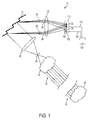
- Figure 1 illustrates imaging system 10 receptive to electromagnetic radiation 20 from target area 30.
- Electromagnetic radiation 20 may be of any suitable type, including but not limited to visible light, infrared light, and ultraviolet light.
- Target area 30 may be any suitable area to be imaged, including but not limited to space-based objects and ground-based objects. Target area 30 may be observed from the ground (i.e. looking across to other ground-based objects, or up to observe other space-based objects), or from space (i.e. looking down upon ground-based objects, or across to other space-based objects). In various situations, target area 30 may be other satellites, stellar objects, earth based mineral deposits, forests, deserts, bodies of water, or any other body that reflects or emits electromagnetic radiation 20.
- imaging system 10 may be mounted to a satellite. In other embodiments, imaging system 10 may be mounted to manned or un-manned airplanes.
- imaging system 10 may comprise fore-optics 40 which may focus, shape, or otherwise enhance electromagnetic radiation 20.
- fore-optics 40 may comprise a telescope, one or more lenses, or one or more mirrors.
- imaging system 10 comprises slit 50
- fore-optics 40 may be configured to focus electromagnetic radiation 20 at slit 50.
- imaging system 10 may further comprise collimator 60, configured to align electromagnetic radiation 20.
- collimator 60 may be of any construction or configuration, including but not limited to comprising one or more lenses and/or one or more mirrors.
- collimator 60 may be positioned to receive electromagnetic radiation 20 as electromagnetic radiation 20 defocuses following passage through slit 50.
- the collimator 60 is configured to align the electromagnetic radiation prior to the dispersive element receiving the electromagnetic radiation.
- imaging system 10 further comprises dispersive element 70 configured to receive electromagnetic radiation 20.
- Dispersive element 70 is configured to disperse a non-zero order of electromagnetic radiation 20 into constituent spectra 80.
- Dispersive element 70 is further configured to reflect a zero order of electromagnetic radiation 20 as reflected electromagnetic radiation 90.
- dispersive element 70 may be any suitable optical device configured to both disperse and reflect electromagnetic radiation 20.
- dispersive element 70 may comprise diffraction grating.
- dispersive element 70 may permit spatial coincidence of spectra 80 and reflected electromagnetic radiation 90. Dispersive element 70 is described in greater detail below.
- imaging system 10 may further comprise imager optics 100.
- imager optics 100 are configured to focus, shape, or otherwise enhance spectra 80 and reflected electromagnetic radiation 90 onto focal plane 110.
- focal plane 110 may comprise first focal plane array 120 and second focal plane array 130.
- First focal plane array 120 and second focal plane array 130 may each be any suitable imaging array, including but not limited to a charge-coupled device (CCD), a Complimentary Metal-Oxide-Semiconductor (CMOS) based image sensor, a Mercury Cadmium Telluride (HgCdTe) based sensor, an Indium Antimonite (InSb) based sensor, or an Indium Gallium Arsenide (InGaAs) based sensor.
- CCD charge-coupled device
- CMOS Complimentary Metal-Oxide-Semiconductor
- HgCdTe Mercury Cadmium Telluride
- InSb Indium Antimonite
- InGaAs Indium Gallium Ars
- spectra 80 may be focused onto first focal plane array 120, while reflected electromagnetic radiation 90 may be focused onto second focal plane array 130.
- first focal plane array 120 and second focal plane array 130 may be of the same length, corresponding to a spatial dimension of target area 30, however first focal plane array 120 may be of a greater width, configured to receive a determined wavelength range of spectra 80.
- first focal plane array 120 may be sensitive to hyperspectral wavelength ranges.
- polarity discriminating element 140 associated with second focal plane array 130.
- polarity discriminating element 140 may be configured to permit determination of a polarization of electromagnetic radiation 20, as reflected as reflected electromagnetic radiation 90.
- reflected electromagnetic radiation 90 is reflected directly or indirectly through polarity discriminating element 140, whereby it is received by second focal plane array 130 as polarity discriminated electromagnetic radiation 150.
- Polarity discriminating element 140 is described in greater detail below.
- first focal plane array 120 and second focal plane array 130 may be constituent parts of a single focal plane array element.
- the polarity discriminating element 140 may be associated with only second focal plane array 130 of the single focal plane array element.
- Imaging system 10 may further comprise classifier 160.
- classifier 160 may be receptive to spectra 80 as received on first focal plane array 120 and polarity discriminated electromagnetic radiation 150 as received on second focal plane array 130.
- classifier 160 may be receptive to spectral data 170 read out from first focal plane array 120, and receptive to polarimetric data 180 read out from second focal plane array 130.
- first focal plane array 120 and second focal plane array 130 may share a common readout clock.
- the common readout clock may be part of classifier 160.
- the common readout clock may comprise a first readout clock associated with first focal plane array 120, and a second readout clock associated with second focal plane array 130.
- the first and second readout clocks may be synchronized.
- the common readout clock which may or may not comprise first and second readout clocks, may be part of classifier 160.
- the common readout clock may permit temporal coincidence of spectral data 170 and polarimetric data 180. In an embodiment, the common readout clock may correlate spectral data 170 and polarimetric data 180. In an embodiment, the classifier 160 and/or the common readout clock may be configured to spatially and temporally co-register spectral data 170 and polarimetric data 180
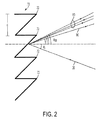
- FIG. 2 shows a schematic of electromagnetic radiation 20 incident on dispersive element 70.
- dispersive element 70 comprises a diffraction grating having peaks 72 of spacing d.
- Various other configurations of dispersive element 70 are also possible, including but not limited to grooves, slits, pits, or any other suitable element having a periodic structure to disperse and reflect electromagnetic radiation 20.
- incident electromagnetic radiation 20 may be emitted or reflected onto dispersive element 70, at an incident angle of 0;. Due to the shape and geometry of dispersive element 70, electromagnetic radiation 20 may be reflected and/or dispersed off of dispersive element 70 at a variety of orders m.
- ⁇ o sin -1 (( m ⁇ / d ) - sin ( ⁇ i )).
- electromagnetic radiation 20 is broken into constituent spectra 80 that is dispersed at different angles for each wavelength ⁇ .
- dispersive element 70 may permit spatial coincidence of spectra 80 and reflected electromagnetic radiation 90.
- spectra 80 may be received on first focal plane array 120 to be interpreted as spectral data 170.
- reflected electromagnetic radiation 90 may be received by second focal plane array 130, through polarity discriminating element 140, to obtain polarimetric data 180.
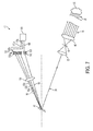
- Figure 3 and Figure 4 show alternative embodiments of the configuration of second focal plane array 130 and polarity discriminating element 140 to obtain polarimetric data 180.
- Figure 3 shows an embodiment of an in-scan motion smear configuration of the second focal plane array 130 and associated polarity discriminating element 140.
- reflected electromagnetic radiation 90 is shown originating from different field points as electromagnetic radiation 90a-d.
- the electromagnetic radiation 90a-d may pass through the polarity discriminating element 140, wherein polarity discriminated electromagnetic radiation may selectively filter some of reflected electromagnetic radiation 90, permitting polarity discriminated electromagnetic radiation 150 (i.e. polarity discriminated electromagnetic radiation 150a and 150d based on their originating field points) through to second focal plane array 130.
- discriminated electromagnetic radiation 150 may be received on second focal plane array 130 over a plurality of pixels 190. More details of the configuration of the polarity discriminating element 140 are provided below.
- Figure 4 shows another embodiment of second focal plane array 130 and associated polarity discriminating element 140, arranged in a pupil imager configuration.
- reflected electromagnetic radiation 90 may be directed to converge at focal plane 110, before diverging and intersecting micro-lens 200.
- micro-lens 200 may be configured to "scramble" and direct electromagnetic radiation 90 towards second focal plane array 130 through associated polarity discriminating element 140.
- polarity discriminated electromagnetic radiation 150 may be permitted to pass through polarity discriminating element 140, to be received on second focal plane array 130, and output as polarimetric data 180.
- the polarity discriminating element 140 may be configured to permit determination of a polarization of electromagnetic radiation 20, as reflected as reflected electromagnetic radiation 90.
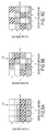
- Figures 5A-C schematically show various embodiments of at least a portion of polarity discriminating element 140.
- polarity discriminating element 140 may comprise a plurality of polarizing filters 140(x,y), wherein (x,y) is the numerical position on the demarked x and y coordinates of polarity discriminating element 140 in Figures 5A-C .
- polarity discriminating element 140 may be characterized as a polarization filtering analogy of a Bayer filter (i.e. an RGBW filter).
- polarizing filters 140(x,1) are circularly polarized
- polarizing filters 140(x,2) are linearly polarized at 45 degrees
- polarizing filters 140(x,3) are linearly polarized.
- polarizing filters 140(x,4) do not actually filter based on polarization, but instead permit all reflected electromagnetic radiation 90 incident on those polarizing filters 140(x,4) to be received by second focal plane array 130.
- similar polarization filters 140(x,y) may be offset by one element in the in-scan dimension (i.e. the y axis).
- similar polarization filters 140(x,y) may be offset by two elements in the in-scan dimension. These embodiments are not limiting, and in other embodiments, a variety of patterns of polarization filters 140(x,y) may be utilized. In an embodiment, there may be an equal number of polarization filters 140(x,y) in each of unfiltered reflected electromagnetic radiation 90, circularly polarized, linearly polarized, and linearly polarized ⁇ 45 degrees. Other combinations of polarization filters 140(x,y) are possible, including, as one non-limiting example, the use of three polarization filters 140(x,y), polarized at 0 degrees, 60 degrees, and 120 degrees respectively.
- each of polarization filters 140(x,y) may correspond to each of plurality of pixels 190 of second focal plane array 130, such that polarization filter 140(x,y) is associated with pixel 190(x,y).
- reflected electromagnetic radiation 90 incident on polarization filter 140(x,y), that is permitted through polarization filter 140(x,y) may then be received by associated pixel 190(x,y) of second focal plane array 130.
- classifier 160 knows the associated polarization filter 140(x,y) for each pixel 190(x,y). For example, classifier 160 may have access to a database listing in a memory device (not shown) of associated polarization filters 140 for each of the plurality of pixels 190.
- Stokes parameters for the electromagnetic radiation 20 of the target area 30 may be ascertained.
- classifier 160 may characterize a reading from pixel elements 190(x,4) as irradiance data E 0 .
- classifier 160 may characterize a reading from pixel elements 190(x,3) as linear horizontal polarization data E 1 .
- classifier 160 may characterize a reading from pixel elements 190(x,2) as linear +45 degree polarization data E 2 .
- classifier 160 may characterize a reading from pixel elements 190(x,1) as circular polarization data E 3 .
- the polarization state of electromagnetic radiation 20 from the target area 30 may be computed, including, for example, the degree of polarization and the degree of linear polarization.
- the degree of polarization is then (S 1 2 + S 2 2 + S 3 2 ) 1 ⁇ 2 / S 0
- the degree of linear polarization would then be (S 1 2 + S 2 2 ) 1 ⁇ 2 / S 0 .
- the classifier 160 may be configured to compute one or more of the Stokes parameters, the degree of polarization of electromagnetic radiation 20, and the degree of linear polarization of electromagnetic radiation 20.
- Figure 7 provides a schematic of an alternative embodiment of imaging system 10.
- electromagnetic radiation 20 emitted from target area 30 may be received by fore-optics 40.
- Fore-optics 40 may shape or enhance electromagnetic radiation 20, where in an embodiment it may be focused on slit 50, before dispersing.
- electromagnetic radiation 20 may then be aligned by collimator 60, and directed towards dispersive element 70, which may be any suitable optical device configured to both disperse and reflect electromagnetic radiation 20.
- dispersive element 70 remains configured to reflect a zero order of electromagnetic radiation 20 as reflected electromagnetic radiation 90, where it may pass through imager optics 100, which may focus, shape or enhance reflected electromagnetic radiation 90 through polarity discriminating element 140 onto second focal plane array 130.
- Dispersive element 70 is also again configured to disperse non-zero orders of electromagnetic radiation 20 into constituent spectra 80.
- dispersive element 70 may also be configured to direct electromagnetic radiation 20 in multiple discrete wavelength bands over multiple diffraction orders.
- dispersive element 70 may be configured to diffract and disperse longer wavelength electromagnetic radiation 20 using a low diffraction order, while diffracting and dispersing shorter wavelength electromagnetic radiation 20 using a higher diffraction order.
- Such a configuration may result in electromagnetic radiation of different wavelengths being diffracted with the same geometry (i.e. at the same angle).
- three exemplary rays of spectra 80 are depicted, each representing electromagnetic radiation 20 being diffracted at angle ⁇ o .
- Figure 7 further shows that in such an embodiment, spectra 80 may be received by first focal plane array 120, wherein first focal plane array 120 is a two-color focal plane array having both upper active area 120a and lower active area 120b.
- first focal plane array 120 is a two-color focal plane array having both upper active area 120a and lower active area 120b.
- the use of the term two-color focal plane array is defined as a focal plane array having at least an upper and lower active area 120a and 120b, and may comprise intermediate active areas, such that the focal plane array is sensitive to more than two-colors.
- first focal plane array 120 is configured with both upper active area 120a and lower active area 120b.
- both upper active area 120a and lower active area 120b may be configured to generate spectral data 170, including upper active area spectral data 170a and lower active area spectral data 170b.
- imaging system 10 may further comprise classifier 160.
- Classifier 160 may be any suitable system, including but not limited to one comprising or implemented by an appropriate algorithm operating on a processor, a programmed computer system, a computer network, or a database system.
- classifier 160 may be a standalone computer connected to first and second focal plane arrays 120 and 130, or an embedded processor that may be part of imaging system 10, such as part of first and second focal plane arrays 120 and 130.
- classifier 160 may be receptive to spectra 80, as received on upper active area 120a and lower active area 120b of first focal plane array 120, and polarity discriminated electromagnetic radiation 150, as received on second focal plane array 130.
- classifier 160 may be receptive to spectral data 170 read out from first focal plane array 120, which in an embodiment may comprise upper active area spectral data 170a read out from upper active area 120a, and lower active area spectral data 170b read out from lower active area 120b.
- the classifier 160 may be receptive to polarimetric data 180 read out from second focal plane array 130.
- upper active area 120a and lower active area 120b may share a common readout clock.
- upper active area 120a, lower active area 120b, and second focal plane array 130 may share the common readout clock.
- the common readout clock may be part of classifier 160.
- the common readout clock may comprise a first readout clock associated with upper active area 120a and lower active area 120b of first focal plane array 120, and a second readout clock associated with second focal plane array 130.
- the first and second readout clocks may be synchronized.
- the common readout clock which may or may not comprise first and second readout clocks, may be part of classifier 160.
- the common readout clock may permit temporal coincidence of spectral data 170 (including upper active area spectral data 170a and lower active area spectral data 170b) and polarimetric data 180. In an embodiment, the common readout clock may correlate upper active area spectral data 170a and lower active area spectral data 170b. In an embodiment, the common readout clock may correlate upper active area spectral data 170a, lower active area spectral data 170b, and polarimetric data 180.
- the classifier 160 and/or the common readout clock may be configured to spatially and temporally co-register spectral data 170 (which may include both upper active area spectral data 170a and lower active area spectral data 170b) and polarimetric data 180.
- Method 300 may start at 302, and may include at step 310 selecting target area 30.
- target area 30 may be may be any suitable area to be imaged, including but not limited to space-based objects and ground-based objects, observed from any suitable location, including the ground, the air, or from space.
- the selection of target area 30 at step 310 may be deliberate, such as with a targeting system, or by chance, such as in a data-gathering survey.
- method 300 may continue at step 320 by receiving electromagnetic radiation 20 on dispersive element 70, wherein dispersive element 70 is configured to diffract electromagnetic radiation 20 into zero-order electromagnetic radiation (i.e. reflected electromagnetic radiation 90) and at least one non-zero order electromagnetic radiation (i.e. spectra 80).
- Receiving electromagnetic radiation 20 on dispersive element 70 may be through any suitable intermediary, including receiving electromagnetic radiation 20 through fore-optics 40, which may include a telescope or any other optical element configured to shape, focus, or enhance electromagnetic radiation 20.
- receiving electromagnetic radiation 20 on dispersive element 70 may further comprise collimating electromagnetic radiation 20.
- Method 300 may also include at step 330 receiving non-zero electromagnetic radiation (i.e. spectra 80) on first focal plane array 120.
- receiving non-zero polarimetric radiation on first focal plane array 120 may comprise dispersing, with dispersive element 70, electromagnetic radiation 20 into spectra 80.
- non-zero electromagnetic radiation, such as spectra 80 may be focused through imager optics 100 before being received on first focal plane array 120.
- imager optics 100 may be configured to focus, shape, or otherwise enhance spectra 80 and onto first focal plane array 120.
- first focal plane array 120 may comprise a two-color focal plane array having upper active area 120a and lower active area 120b, wherein receiving the non-zero order electromagnetic radiation at step 330 may comprise receiving a shorter wavelength band of electromagnetic radiation on upper active area 120a, and receiving a longer wavelength band of electromagnetic radiation on lower active area 120b.
- a further element of method 300 may comprise at step 340 polarizing zero order electromagnetic radiation (i.e. reflected electromagnetic radiation 90) into polarized electromagnetic radiations 150, with a polarizing element configured to permit determination of a polarization of electromagnetic radiation 20.
- the polarizing element may be similar to or comprise polarity discriminating element 140 described above, and may comprise a plurality of polarizing filters 140(x,y) as depicted in Figure 5A-C .
- the polarized electromagnetic radiations may comprise polarity discriminated electromagnetic radiation 150.
- the polarizing element may permit determination of the Stokes vectors for electromagnetic radiation 20, so as to permit determination of the degree of polarization and/or the degree of linear polarization of electromagnetic radiation 20.
- Method 300 may continue to include at step 350 receiving the polarized electromagnetic radiation, such as polarity discriminated electromagnetic radiations 150 on second focal plane array 130.
- receiving the polarized electromagnetic radiation may comprise utilizing the in-scan motion smear configuration of the second focal plane array 130 and associated polarity discriminating element 140.
- polarity discriminated electromagnetic radiation 150 may be received on second focal plane array 130 over a plurality of pixels 190.
- receiving the polarized electromagnetic radiation at step 350 may comprise utilizing the pupil imager configuration of the second focal plane array 130 and the polarizing element (such as the polarity discriminating element 140).
- reflected electromagnetic radiation 90 may be directed to converge at focal plane 110, before diverging and intersecting micro-lens 200, which may be configured to scramble electromagnetic radiation 90, and direct it towards second focal plane array 130, through associated polarity discriminating element 140.
- Step 360 of method 300 may proceed to include synchronously reading out hyperspectral data 170 from first focal plane array 120 and polarimetric data 180 from second focal plane array 130.
- a synchronous read-out of data from the first and second focal plane arrays 120 and 130 may comprise using classifier 160.
- step 360 may comprise utilizing a common readout clock.
- step 360 may comprise utilizing a first readout clock associated with first focal plane array 120 and a second readout clock associated with second focal plane array 130, wherein the first and second readout clocks are synchronized with one another.
- first focal plane array 120 is a two-color focal plane array comprising upper active area 120a and lower active area 120b
- synchronously reading out hyperspectral data 170 and polarimetric data 180 at step 360 may comprise utilizing a common readout clock shared by each of upper active area 120a, lower active area 120b, and second focal plane array 130.
- Method 300 may then continue at step 370 by determining the polarization of electromagnetic radiation 20.
- this determination may be calculated by classifier 160, or by any other process.
- determination of the polarization of electromagnetic radiation 20 may include determining the degree of polarization and/or the degree of linear polarization.
- this data may be spatially and/or temporally co-registered with the hyperspectral data.
- This data may in an embodiment be output in any suitable form, including but not limited to an image, a chart, an animation, or so on.
- the hyperspectral data 170 and polarimetric data 180 may be compared to a database to identify a likely candidate for the material in target area 30 that is the reflective or emissive source of electromagnetic radiation 20.
- method 300 may end at step 380.
- inventive concept has been described in detail for the purpose of illustration based on what is currently considered to be the most practical and useful embodiments, it is to be understood that such detail is solely for that purpose and that the inventive concept is not limited to the disclosed embodiments, but, on the contrary, is intended to cover modifications and equivalent arrangements that are within the spirit and scope of the appended claims.
- this disclosure contemplates that, to the extent possible, one or more features of any embodiment can be combined with one or more features of any other embodiment.
Landscapes
- Physics & Mathematics (AREA)
- Spectroscopy & Molecular Physics (AREA)
- General Physics & Mathematics (AREA)
- Investigating Or Analysing Materials By Optical Means (AREA)
- Spectrometry And Color Measurement (AREA)
Applications Claiming Priority (1)
| Application Number | Priority Date | Filing Date | Title |
|---|---|---|---|
| US12/833,926 US8189179B2 (en) | 2010-07-09 | 2010-07-09 | System and method for hyperspectral and polarimetric imaging |
Publications (2)
| Publication Number | Publication Date |
|---|---|
| EP2416136A2 true EP2416136A2 (de) | 2012-02-08 |
| EP2416136A3 EP2416136A3 (de) | 2013-03-27 |
Family
ID=44672070
Family Applications (1)
| Application Number | Title | Priority Date | Filing Date |
|---|---|---|---|
| EP11163920A Ceased EP2416136A3 (de) | 2010-07-09 | 2011-04-27 | System und Verfahren zur hyperspektralen und polarimetrischen Abbildung |
Country Status (3)
| Country | Link |
|---|---|
| US (1) | US8189179B2 (de) |
| EP (1) | EP2416136A3 (de) |
| IL (1) | IL212517A (de) |
Cited By (1)
| Publication number | Priority date | Publication date | Assignee | Title |
|---|---|---|---|---|
| WO2017156400A1 (en) * | 2016-03-10 | 2017-09-14 | Regents Of The University Of Minnesota | Spectral-spatial imaging device |
Families Citing this family (35)
| Publication number | Priority date | Publication date | Assignee | Title |
|---|---|---|---|---|
| US8411146B2 (en) * | 2009-09-04 | 2013-04-02 | Lockheed Martin Corporation | Single camera color and infrared polarimetric imaging |
| US9593982B2 (en) | 2012-05-21 | 2017-03-14 | Digimarc Corporation | Sensor-synchronized spectrally-structured-light imaging |
| US9621760B2 (en) | 2013-06-07 | 2017-04-11 | Digimarc Corporation | Information coding and decoding in spectral differences |
| WO2015077493A1 (en) * | 2013-11-20 | 2015-05-28 | Digimarc Corporation | Sensor-synchronized spectrally-structured-light imaging |
| US9232130B2 (en) * | 2013-12-04 | 2016-01-05 | Raytheon Canada Limited | Multispectral camera using zero-mode channel |
| US9182283B2 (en) * | 2014-04-03 | 2015-11-10 | Raytheon Company | Imaging spectropolarimeter using orthogonal polarization pairs |
| CN104166481B (zh) * | 2014-08-15 | 2017-05-24 | 京东方科技集团股份有限公司 | 一种显示基板及显示装置 |
| US10113910B2 (en) | 2014-08-26 | 2018-10-30 | Digimarc Corporation | Sensor-synchronized spectrally-structured-light imaging |
| JP2016171368A (ja) * | 2015-03-11 | 2016-09-23 | 株式会社東芝 | 撮像装置、撮像素子、及び撮像方法 |
| US10168542B2 (en) * | 2015-08-26 | 2019-01-01 | Raytheon Company | Polarized pixelated filter array with reduced sensitivity to misalignment for polarimetric imaging |
| EP3443309A4 (de) * | 2016-04-11 | 2019-12-18 | Polaris Sensor Technologies, Inc. | Kurzwellen-infrarotkamera |
| MY195255A (en) | 2016-06-30 | 2023-01-11 | Sicpa Holding Sa | Systems and Methods for Imaging an Object and Generating a Measure of Authenticity of The Object |
| US10890485B2 (en) | 2016-06-30 | 2021-01-12 | Sicpa Holding Sa | Systems, methods, and computer programs for generating a measure of authenticity of an object |
| CN114286953B (zh) | 2019-07-26 | 2025-04-01 | 梅特兰兹股份有限公司 | 孔隙-超表面和混合折射-超表面成像系统 |
| US11042025B2 (en) | 2019-09-20 | 2021-06-22 | Raytheon Company | Optical data communication using micro-electro-mechanical system (MEMS) micro-mirror arrays |
| US11539131B2 (en) | 2020-08-24 | 2022-12-27 | Raytheon Company | Optical true time delay (TTD) device using microelectrical-mechanical system (MEMS) micromirror arrays (MMAS) that exhibit tip/tilt/piston (TTP) actuation |
| US11837840B2 (en) | 2020-09-01 | 2023-12-05 | Raytheon Company | MEMS micro-mirror array laser beam steerer for simultaneous illumination of multiple tracked targets |
| US11815676B2 (en) | 2020-09-17 | 2023-11-14 | Raytheon Company | Active pushbroom imaging system using a micro-electro-mechanical system (MEMS) micro-mirror array (MMA) |
| US11522331B2 (en) | 2020-09-23 | 2022-12-06 | Raytheon Company | Coherent optical beam combination using micro-electro-mechanical system (MEMS) micro-mirror arrays (MMAs) that exhibit tip/tilt/piston (TTP) actuation |
| US12372658B2 (en) | 2020-10-12 | 2025-07-29 | Raytheon Company | Negative obstacle detector using micro-electro-mechanical system (MEMS) micro-mirror array (MMA) beam steering |
| US11477350B2 (en) | 2021-01-15 | 2022-10-18 | Raytheon Company | Active imaging using a micro-electro-mechanical system (MEMS) micro-mirror array (MMA) |
| US12066574B2 (en) | 2021-01-15 | 2024-08-20 | Raytheon Company | Optical system for object detection and location using a Micro-Electro-Mechanical System (MEMS) Micro-Mirror Array (MMA) beamsteering device |
| US11550146B2 (en) | 2021-01-19 | 2023-01-10 | Raytheon Company | Small angle optical beam steering using micro-electro-mechanical system (MEMS) micro-mirror arrays (MMAS) |
| US11835709B2 (en) | 2021-02-09 | 2023-12-05 | Raytheon Company | Optical sensor with micro-electro-mechanical system (MEMS) micro-mirror array (MMA) steering of the optical transmit beam |
| US12372623B2 (en) | 2021-02-17 | 2025-07-29 | Raytheon Company | Conic micro-electro-mechanical system (MEMS) micro-mirror array (MMA) steered active situational awareness sensor |
| US12025790B2 (en) | 2021-02-17 | 2024-07-02 | Raytheon Company | Micro-electro-mechanical system (MEMS) micro-mirror array (MMA) and off-axis parabola (OAP) steered active situational awareness sensor |
| US11921284B2 (en) | 2021-03-19 | 2024-03-05 | Raytheon Company | Optical zoom system using an adjustable reflective fresnel lens implemented with a micro-electro-mechanical system (MEMs) micro-mirror array (MMA) |
| US11483500B2 (en) | 2021-03-24 | 2022-10-25 | Raytheon Company | Optical non-uniformity compensation (NUC) for passive imaging sensors using micro-electro-mechanical system (MEMS) micro-mirror arrays (MMAS) |
| US12130384B2 (en) | 2021-03-30 | 2024-10-29 | Raytheon Company | Multiple field-of-view (FOV) optical sensor using a micro-electro-mechanical system (MEMS) micro- mirror array (MMA) |
| US12061334B2 (en) | 2021-04-15 | 2024-08-13 | Raytheon Company | Optical scanning system using micro-electro-mechanical system (mems) micro-mirror arrays (MMAs) |
| US12360358B2 (en) | 2021-04-22 | 2025-07-15 | Raytheon Company | Micro-electro-mechanical system (MEMS) micro-mirror array (MMA) steered high-power laser transmitter |
| US12117607B2 (en) | 2021-04-28 | 2024-10-15 | Raytheon Company | Micro-electro-mechanical system (MEMS) micro-mirror array steered laser transmitter and situational awareness sensor with wavelength conversion |
| US11644542B2 (en) | 2021-09-20 | 2023-05-09 | Raytheon Company | Optical sensor with MEMS MMA steered transmitter and staring detector |
| US12259277B2 (en) | 2021-09-20 | 2025-03-25 | Raytheon Company | Image polarimeter using a micro-electro-mechanical system (MEMS) micro-mirror array (MMA) |
| KR20240163162A (ko) * | 2022-03-31 | 2024-11-18 | 메탈렌츠 인코포레이티드 | 편광 분류 메타표면 마이크로렌즈 어레이 디바이스 |
Citations (1)
| Publication number | Priority date | Publication date | Assignee | Title |
|---|---|---|---|---|
| US20080161958A1 (en) * | 2006-11-14 | 2008-07-03 | Abb Inc. | System for storing and presenting sensor and spectrum data for batch processes |
Family Cites Families (16)
| Publication number | Priority date | Publication date | Assignee | Title |
|---|---|---|---|---|
| US4650321A (en) * | 1985-07-05 | 1987-03-17 | The Perkin-Elmer Corporation | Spatial/spectral real time imaging |
| US4844617A (en) * | 1988-01-20 | 1989-07-04 | Tencor Instruments | Confocal measuring microscope with automatic focusing |
| DD270133A1 (de) * | 1988-03-11 | 1989-07-19 | Akad Wissenschaften Ddr | Anordnung zur untersuchung hochaufgeloester teilspektren eines echelle-spektrums |
| US5225893A (en) | 1990-12-10 | 1993-07-06 | Hughes Aircraft Company | Two-color focal plane array sensor arrangement |
| IL116583A (en) * | 1995-12-27 | 2001-06-14 | Ruschin Shlomo | Spectral analyzer and directional indicator |
| WO1999002950A1 (en) * | 1997-07-12 | 1999-01-21 | Optical Insights, Llc | Multi-spectral two-dimensional imaging spectrometer |
| US6104488A (en) | 1999-08-12 | 2000-08-15 | The United States Of America As Represented By The Secretary Of The Air Force | Multi-octave spectroscopy with multi-waveband infrared focal plane array |
| US6814441B2 (en) * | 1999-11-18 | 2004-11-09 | Kabushiki Kaisha Topcon | Apparatus for measurement of polarized distribution, polarizing filter for using therein and polarizing filter assembly |
| US20020167727A1 (en) * | 2001-03-27 | 2002-11-14 | Hansen Douglas P. | Patterned wire grid polarizer and method of use |
| JP3958134B2 (ja) * | 2002-07-12 | 2007-08-15 | キヤノン株式会社 | 測定装置 |
| JP2004200358A (ja) | 2002-12-18 | 2004-07-15 | Nikon Corp | 固体撮像素子の色分解装置 |
| JP4499476B2 (ja) * | 2004-05-25 | 2010-07-07 | オリンパス株式会社 | 分光画像入力装置及びそれを備えた光学装置 |
| US7038776B1 (en) | 2005-03-25 | 2006-05-02 | Raytheon Company | Polarimeter to simultaneously measure the stokes vector components of light |
| WO2007070306A2 (en) * | 2005-12-09 | 2007-06-21 | Arete Associates | Miniature integrated multisectral/multipolarization digital camera |
| US7876434B2 (en) * | 2005-12-12 | 2011-01-25 | California Institute Of Technology | Color camera computed tomography imaging spectrometer for improved spatial-spectral image accuracy |
| DE102008014334B4 (de) * | 2008-03-14 | 2009-12-17 | Fraunhofer-Gesellschaft zur Förderung der angewandten Forschung e.V. | Integrierter Polarisationssensor |
-
2010
- 2010-07-09 US US12/833,926 patent/US8189179B2/en not_active Expired - Fee Related
-
2011
- 2011-04-27 IL IL212517A patent/IL212517A/en active IP Right Grant
- 2011-04-27 EP EP11163920A patent/EP2416136A3/de not_active Ceased
Patent Citations (1)
| Publication number | Priority date | Publication date | Assignee | Title |
|---|---|---|---|---|
| US20080161958A1 (en) * | 2006-11-14 | 2008-07-03 | Abb Inc. | System for storing and presenting sensor and spectrum data for batch processes |
Cited By (6)
| Publication number | Priority date | Publication date | Assignee | Title |
|---|---|---|---|---|
| WO2017156400A1 (en) * | 2016-03-10 | 2017-09-14 | Regents Of The University Of Minnesota | Spectral-spatial imaging device |
| US10837830B2 (en) | 2016-03-10 | 2020-11-17 | Regents Of The University Of Minnesota | Spectral-spatial imaging device |
| AU2020202458B2 (en) * | 2016-03-10 | 2021-03-25 | Regents Of The University Of Minnesota | Spectral-spatial imaging device |
| US11187580B2 (en) | 2016-03-10 | 2021-11-30 | Regents Of The University Of Minnesota | Spectral-spatial imaging device |
| AU2021204326B2 (en) * | 2016-03-10 | 2023-04-13 | Regents Of The University Of Minnesota | Spectral-spatial imaging device |
| US12055436B2 (en) | 2016-03-10 | 2024-08-06 | Regents Of The University Of Minnesota | Spectral-spatial imaging device |
Also Published As
| Publication number | Publication date |
|---|---|
| US20120008133A1 (en) | 2012-01-12 |
| IL212517A (en) | 2015-07-30 |
| US8189179B2 (en) | 2012-05-29 |
| IL212517A0 (en) | 2011-07-31 |
| EP2416136A3 (de) | 2013-03-27 |
Similar Documents
| Publication | Publication Date | Title |
|---|---|---|
| US8189179B2 (en) | System and method for hyperspectral and polarimetric imaging | |
| CN101871815B (zh) | 一种基于孔径分割和声光可调谐滤光器的可编程偏振超光谱成像仪 | |
| JP6314232B2 (ja) | 多機能イメージャ | |
| Claudi et al. | SPHERE IFS: the spectro differential imager of the VLT for exoplanets search | |
| US8175393B2 (en) | Multi-phenomenology object detection | |
| US8154732B2 (en) | Multiband spatial heterodyne spectrometer and associated methods | |
| US9097585B2 (en) | Spectrographic polarimeter and method of recording state of polarity | |
| Mu et al. | Demonstration of a snapshot full-Stokes division-of-aperture imaging polarimeter using Wollaston prism array | |
| US11249289B2 (en) | Spectral imager and spectral imaging method | |
| JP2013546000A (ja) | イメージマップ分光偏光法 | |
| CN201497574U (zh) | 一种可编程偏振超光谱成像仪 | |
| EP3877734A2 (de) | Verfahren und system zur polarimetrie unter verwendung statischer geometrischer polarisationsmanipulation | |
| WO2016205565A1 (en) | Gas visualizing methods and systems with birefringent polarization interferometer | |
| US20150156394A1 (en) | Multispectral camera using zero-mode channel | |
| EP1705469B1 (de) | Polarimeter zur gleichzeitigen Messung der Stokes-Parameter von Licht | |
| Kraft et al. | On the demands on imaging spectrometry for the monitoring of global vegetation fluorescence from space | |
| Moskovitz et al. | Observational investigation of the 2013 near-Earth encounter by asteroid (367943) Duende | |
| Rodenhuis et al. | Five-dimensional optical instrumentation: combining polarimetry with time-resolved integral-field spectroscopy | |
| CN201811790U (zh) | 一种集成全色和偏振超光谱探测能力的成像仪 | |
| CN102080987B (zh) | 一种集成全色和偏振超光谱探测能力的成像仪 | |
| US10070080B2 (en) | Multi-directional, multi-spectral star tracker with a common aperture and common camera | |
| CN114777925A (zh) | 一种基于偏振光栅分光的像映射偏振光谱仪 | |
| CN101995293B (zh) | 一种基于像面拼接的可编程偏振超光谱成像仪 | |
| Lucas et al. | Visible-light high-contrast imaging polarimetry at Subaru | |
| Skauli et al. | A compact combined hyperspectral and polarimetric imager |
Legal Events
| Date | Code | Title | Description |
|---|---|---|---|
| AK | Designated contracting states |
Kind code of ref document: A2 Designated state(s): AL AT BE BG CH CY CZ DE DK EE ES FI FR GB GR HR HU IE IS IT LI LT LU LV MC MK MT NL NO PL PT RO RS SE SI SK SM TR |
|
| AX | Request for extension of the european patent |
Extension state: BA ME |
|
| PUAI | Public reference made under article 153(3) epc to a published international application that has entered the european phase |
Free format text: ORIGINAL CODE: 0009012 |
|
| PUAL | Search report despatched |
Free format text: ORIGINAL CODE: 0009013 |
|
| AK | Designated contracting states |
Kind code of ref document: A3 Designated state(s): AL AT BE BG CH CY CZ DE DK EE ES FI FR GB GR HR HU IE IS IT LI LT LU LV MC MK MT NL NO PL PT RO RS SE SI SK SM TR |
|
| AX | Request for extension of the european patent |
Extension state: BA ME |
|
| RIC1 | Information provided on ipc code assigned before grant |
Ipc: G01J 4/04 20060101ALI20130219BHEP Ipc: G01J 3/28 20060101ALI20130219BHEP Ipc: G01J 3/02 20060101AFI20130219BHEP |
|
| 17P | Request for examination filed |
Effective date: 20130903 |
|
| RBV | Designated contracting states (corrected) |
Designated state(s): AL AT BE BG CH CY CZ DE DK EE ES FI FR GB GR HR HU IE IS IT LI LT LU LV MC MK MT NL NO PL PT RO RS SE SI SK SM TR |
|
| 17Q | First examination report despatched |
Effective date: 20160602 |
|
| STAA | Information on the status of an ep patent application or granted ep patent |
Free format text: STATUS: THE APPLICATION HAS BEEN REFUSED |
|
| 18R | Application refused |
Effective date: 20170516 |