EP2409309B1 - High voltage transformer - Google Patents
High voltage transformer Download PDFInfo
- Publication number
- EP2409309B1 EP2409309B1 EP10707367.8A EP10707367A EP2409309B1 EP 2409309 B1 EP2409309 B1 EP 2409309B1 EP 10707367 A EP10707367 A EP 10707367A EP 2409309 B1 EP2409309 B1 EP 2409309B1
- Authority
- EP
- European Patent Office
- Prior art keywords
- high voltage
- transformer
- winding
- voltage
- windings
- Prior art date
- Legal status (The legal status is an assumption and is not a legal conclusion. Google has not performed a legal analysis and makes no representation as to the accuracy of the status listed.)
- Not-in-force
Links
- 238000004804 winding Methods 0.000 claims description 201
- 230000008878 coupling Effects 0.000 claims description 21
- 238000010168 coupling process Methods 0.000 claims description 21
- 238000005859 coupling reaction Methods 0.000 claims description 21
- 239000002356 single layer Substances 0.000 claims description 7
- 239000012809 cooling fluid Substances 0.000 claims description 2
- 239000004020 conductor Substances 0.000 description 38
- 239000011162 core material Substances 0.000 description 22
- 239000010410 layer Substances 0.000 description 14
- 238000010586 diagram Methods 0.000 description 9
- 238000000034 method Methods 0.000 description 7
- 238000009413 insulation Methods 0.000 description 6
- 230000003071 parasitic effect Effects 0.000 description 6
- XEEYBQQBJWHFJM-UHFFFAOYSA-N Iron Chemical compound [Fe] XEEYBQQBJWHFJM-UHFFFAOYSA-N 0.000 description 3
- 238000001816 cooling Methods 0.000 description 3
- 230000000694 effects Effects 0.000 description 2
- 229910000859 α-Fe Inorganic materials 0.000 description 2
- 239000004952 Polyamide Substances 0.000 description 1
- 238000010276 construction Methods 0.000 description 1
- 230000002500 effect on skin Effects 0.000 description 1
- 239000012717 electrostatic precipitator Substances 0.000 description 1
- 230000004907 flux Effects 0.000 description 1
- 238000010438 heat treatment Methods 0.000 description 1
- 229910052742 iron Inorganic materials 0.000 description 1
- 239000003208 petroleum Substances 0.000 description 1
- 229920002647 polyamide Polymers 0.000 description 1
- 238000005507 spraying Methods 0.000 description 1
Images


Classifications
-
- H—ELECTRICITY
- H01—ELECTRIC ELEMENTS
- H01F—MAGNETS; INDUCTANCES; TRANSFORMERS; SELECTION OF MATERIALS FOR THEIR MAGNETIC PROPERTIES
- H01F38/00—Adaptations of transformers or inductances for specific applications or functions
- H01F38/16—Cascade transformers, e.g. for use with extra high tension
-
- H—ELECTRICITY
- H01—ELECTRIC ELEMENTS
- H01F—MAGNETS; INDUCTANCES; TRANSFORMERS; SELECTION OF MATERIALS FOR THEIR MAGNETIC PROPERTIES
- H01F27/00—Details of transformers or inductances, in general
- H01F27/34—Special means for preventing or reducing unwanted electric or magnetic effects, e.g. no-load losses, reactive currents, harmonics, oscillations, leakage fields
- H01F27/38—Auxiliary core members; Auxiliary coils or windings
-
- H—ELECTRICITY
- H01—ELECTRIC ELEMENTS
- H01F—MAGNETS; INDUCTANCES; TRANSFORMERS; SELECTION OF MATERIALS FOR THEIR MAGNETIC PROPERTIES
- H01F30/00—Fixed transformers not covered by group H01F19/00
- H01F30/04—Fixed transformers not covered by group H01F19/00 having two or more secondary windings, each supplying a separate load, e.g. for radio set power supplies
-
- H—ELECTRICITY
- H01—ELECTRIC ELEMENTS
- H01F—MAGNETS; INDUCTANCES; TRANSFORMERS; SELECTION OF MATERIALS FOR THEIR MAGNETIC PROPERTIES
- H01F27/00—Details of transformers or inductances, in general
- H01F27/28—Coils; Windings; Conductive connections
- H01F27/2823—Wires
- H01F2027/2833—Wires using coaxial cable as wire
-
- H—ELECTRICITY
- H01—ELECTRIC ELEMENTS
- H01F—MAGNETS; INDUCTANCES; TRANSFORMERS; SELECTION OF MATERIALS FOR THEIR MAGNETIC PROPERTIES
- H01F27/00—Details of transformers or inductances, in general
- H01F27/08—Cooling; Ventilating
- H01F27/10—Liquid cooling
-
- H—ELECTRICITY
- H01—ELECTRIC ELEMENTS
- H01F—MAGNETS; INDUCTANCES; TRANSFORMERS; SELECTION OF MATERIALS FOR THEIR MAGNETIC PROPERTIES
- H01F27/00—Details of transformers or inductances, in general
- H01F27/34—Special means for preventing or reducing unwanted electric or magnetic effects, e.g. no-load losses, reactive currents, harmonics, oscillations, leakage fields
Definitions
- This invention relates to a high voltage transformer. More particularly it concerns a high voltage transformer for cascade connection where the high voltage transformer comprises a primary winding, a high voltage winding and a transformer core and wherein the primary winding and the high voltage winding encircles at least a part of the transformer core.
- the term "good high frequency qualities" is used.
- a so-called “pulse transformer” having relatively low coupling inductance between the primary and secondary windings, relatively low so-called “skin effect” and “proximity effect” in the windings at relatively high frequencies, relatively low parasitic capacitance internally in the windings and relatively low capacitance between windings and between windings and the transformer core. This concerns particularly the high voltage winding. Said physical parameters are well known to a person well versed in the art and are therefore not explained further.
- core materials having low electrical conductivity such as ferrite, iron powder or so-called “tape wound cores”.
- a method for feeding the transformer at relatively high frequency comprises a so-called SMPS - (Switched Mode Power Supply) technique.
- the input power is according to this technique converted to a preferably square pulse high frequency input voltage to the high voltage transformer.
- a prior art high voltage transformer has as mentioned, due to its mode of operation, a relatively high number of turns in the secondary winding. This causes an increased secondary capacitance in that the windings with many layers of relatively thin winding wire have less mutual average distance from each other than in a transformer where the winding wire is of larger diameter.
- the many turns of the secondary winding requires relatively much space and thereby leads to the transformer core and the primary winding being relatively large.
- large insulation distances are required between high voltage winding, primary winding and transformer core.
- the transformer thus being relatively large leads to increased losses in transformer windings and also that high voltage transformers of this kind have a relatively low coupling factor.
- a low coupling factor may be modelled as a relatively large coupling inductance. The reason is that a relatively large distance between the primary and secondary windings leads to poor magnetic coupling between them.
- Known low voltage SMPS technique can produce voltages up to the order of 1 kV. At higher voltages it is necessary to adapt the transformer by means of per se known techniques as voltage multiplication, cascade coupled high frequency transformers, layered winding techniques or so-called "resonant switching" to compensate for the relatively narrow bandwidth in a high frequency transformer.
- US patent 7274281 deals with a transformer for a discharge lamp such as a fluorescent tube where the transformer is provided with two series connected primary windings that may be constituted by one winding layer.
- US 1680910 describes a transformer for cascade connection. This one is however not suitable for SMPS because it has a high capacitance in the windings and a low coupling factor.
- US 4518941 shows a transformer that is suitable for SMPS but where the rated transformer ratio is one to one.
- the transformer according to this document is not suitable as a high voltage transformer.
- US 3678429 shows a high voltage transformer for cascade coupling wherein there besides a primary winding and a secondary winding is arranged a winding for cascade coupling. Due to the design of the high voltage winding the transformer according to US 3678429 is not suitable for SMPS.
- US 3579078 deals with a one-step transformer coupled to a so-called "Voltage Quadrupler".
- the transformer does not however solve the relevant technical problem as one does not achieve a high enough voltage in one step.
- US 4023091 discloses a high voltage transformer for cascade coupling, wherein the high voltage transformer comprises a primary winding, a high voltage winding, and a transformer core, and wherein the primary and high voltage windings encircles concentrically at least a part of the transformer core, and where the high voltage transformer is provided with a secondary winding separated from the high voltage winding, as the high voltage winding comprises one single layer or more single layers connected in parallel.
- Prior art does not exhibit transformers having suitable high voltage properties and at the same time being suitable for cascade coupling.
- the object of the invention is to remedy or reduce at least one of the prior art drawbacks.
- a high voltage transformer for cascade coupling where the high voltage transformer comprises a primary winding, a high voltage winding and a transformer core and where the primary and high voltage windings encircles concentrically at least a part of the transformer core, and where the high voltage transformer is provided with a secondary winding as the high voltage winding comprises one single layer or more parallel-connected single layers, and where a secondary winding of a first transformer is connected in series with a primary winding of a second transformer, wherein the high voltage winding of a first transformer is connected in series with a high voltage winding of the second transformer.
- the voltage over the primary and the secondary winding is low-tension relative to the high voltage winding.
- the secondary winding is arranged to carry a larger power than the high voltage winding.
- the high voltage winding is also a secondary winding, but the term high voltage winding is used to better differentiate this winding from the relatively low-voltage secondary winding.
- annular opening for cooling fluid running therethrough.
- Such an opening between the windings and the transformer core ensures at the same time the necessary insulation distance and results in relatively low capacitance between windings and between windings and the transformer core.
- L m is primary magnetising inductance
- kp is coupling factor
- N sek is coupling factor
- C s is total parasitic capacitance in the secondary winding.
- the series resonant frequency is a direct measure of how good the high frequency properties of the transformer are.
- M is the number of the relevant step and N is number of steps.
- the high voltage winding being wound of a relatively thin winding wire limits the power it can supply.
- This drawback is compensated to a considerable extent by that a transformer according to the invention has a considerably improved efficiency compared to prior art transformers, and that the thin winding wire makes room for a cooling slit between the windings and between the windings and the transformer core making good cooling and electric insulation between the components possible.
- the transformer according to the invention is used in a cascade coupling as described above, the power trough-put in the high voltage winding is reduced considerably relative to prior art, whereby the drawback with high resistance in the high voltage winding is remedied further.
- the high voltage winding may be between the primary winding and the secondary winding in the high voltage transformer.
- the high voltage apparatus may thus comprise two or more cascade coupled transformers.
- the power output on the high voltage side thereby divides itself on high voltage windings in more steps, where most of the steps must be rectified before series connection to avoid that the high voltage winding in one step must drive parasitic capacitance in windings in the next step.
- each high voltage winding may be dimensioned for a fraction of the output power, as the number of steps decide the fraction factor.
- the high voltage winding of the first transformer may cooperate with a voltage multiplier of a per se known kind.
- the second transformer and further transformers in the cascade coupling may also cooperate with each of their own voltage multiplier.
- a high voltage winding with only one layer contributes to an increased insulation distance between the layers in that the high voltage winding takes up little room.
- the thin tubular design of the windings contributes to good cooling of both windings and transformer core, and renders the transformer possible to handle a relatively high power relative to its physical size. By the inner parts being cooled well in this way, and also that internal heating in one-layer windings is avoided, the transformer is also suitable for use under relatively high ambient temperatures.
- More transformers interconnected in a cascade coupling according to the invention is suitable both for high voltage direct current and a combined direct and alternating current output, as one step may be designed without rectification. Since primary driving voltage is conducted via low voltage windings through all steps, it is possible to use this alternating voltage to drive one or more additional transformers in a high voltage cascade having differently rated transformer ratios between the windings to generate different voltages that may be needed in a system.
- a secondary voltage on the last step may for example drive an additional transformer generating filament voltage for an X-ray tube. If so, this is a separate low voltage alternating voltage or a rectified alternating voltage superimposed on the high voltage.
- the transformer of the invention is particularly suitable for use in miniature high voltage power supplies. It occupies relatively little room, puts up with relatively high ambient temperatures and may be formed having a lengthy cylindrical shape, and where there is a need for high voltage direct current or high voltage direct current with superimposed alternating current.
- the transformer may thus suit applications such as in petroleum wells, spraying plants, X-ray apparatuses, electrostatic precipitators and non-thermal plasma generating.
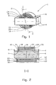
- the reference numeral 1 indicates a high voltage apparatus with a transformer 2.
- the transformer 2 comprises two opposing E-shaped ferrite transformer cores 4 where about and spaced from the mid portions 6 of the transformer cores 4 is coiled a primary winding 8 on a cylindrical, insulating primary sleeve 10.
- the first conductor end portion 12 and the second conductor end portion 14 of the primary winding 8 are led out on the same end portion of the primary winding 8.
- a high voltage winding 16 encircles the primary winding 8 at a radial distance.
- the high voltage winding 16 is wound in one layer on a cylindrical, insulating high voltage sleeve 18.
- the first conductor end portion 20 and the second conductor end portion 22 of the high voltage winding 16 are led out on one each end portion at the high voltage winding 16.
- a secondary winding 24 encircles the high voltage winding 16 at a radial distance.
- the secondary winding 24 is wound on a cylindrical, insulating secondary sleeve 26.
- the first conductor end portion 28 and the second conductor end portion 30 of the secondary winding 24 are led out on the same end portion at the secondary winding 24.
- the secondary winding 24 is also encircled by a static-shield winding 32 connected to the transformer core 4.
- a static-shield winding 32 encircles most of the secondary winding 24, but not completely encircling this, as this if so would constitute a short-circuit turn for the transformer 2.
- the static-shield winding 32 is arranged to improve the high voltage insulation relative to in figs. 1 and 2 adjacent and not shown components.
- the primary winding 8 and the secondary winding 24 have approximately the same number of turns, while the high voltage winding 16 has a considerably higher number of turns.
- the different windings are interconnected by means of not shown per se known circuit board electrical path.
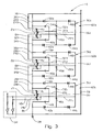
- the transformer 2 is suitable for being fed with an inverted direct voltage from an SMPS power source 34 connected to the first conductor end portion 12 and the second conductor end portion 14 of the primary winding 8 corresponding to what is shown in the diagram in fig. 3 .
- an alternating voltage may be taken out on the first conductor end portion 20 and the second conductor end portion 22 of the high voltage winding 16 and an alternating voltage corresponding to the feed voltage on the first conductor end portion 28 and the second conductor end portion 30 of the secondary winding 24.
- the circuit diagram in fig. 3 shows that the high voltage apparatus 1 in this embodiment besides a first transformer 2 1 also comprises a second transformer 2 2 and a third transformer 2 3 .
- the second transformer 2 2 and the third transformer 2 3 have the same design as the first transformer 2 1 .
- the SMPS power source 34 is connected to the first conductor end portion 12 1 and the second conductor end portion 14 1 of the primary winding 8 1 of the first transformer 2 1 .
- the secondary winding 24 1 of the first transformer 2 1 is by means of the first conductor end portion 28 1 connected to the first conductor end portion 12 2 on the primary winding 8 2 of the second transformer 2 2 .
- the second conductor end portion 30 1 of the secondary winding 24 1 is correspondingly connected to the second conductor end portion 14 2 of the primary winding 8 2 .
- the first conductor end portion 28 2 of the secondary winding 24 2 is connected to the first conductor end portion 12 3 of the primary winding 8 3 and the second conductor end portion 30 2 of the secondary winding 24 2 is connected to the second conductor end portion 14 3 of the primary winding 8 3 .
- the first conductor end portion 28 3 and the second conductor end portion 30 3 of the secondary winding 24 3 of the third transformer 2 3 are connected together to a so-called dummy load 36 having a relatively large electrical resistance. All the second conductor end portions 22 1 , 22 2 , 22 3 of the high voltage windings 16 1 , 16 2 , 16 3 are connected to the corresponding transformer core 4 1 , 4 2 , 4 3 constituting local 0-levels.
- the SMPS power source 34 is earthed to an earth point 38.
- a first condenser 40 1 is connected to the first transformer 2 1 between the second conductor end portion 22 1 and the earth point 38 of the high voltage winding 16 1 .
- a first anode of diode 42 1 is also connected to the earth point 38.
- the first cathode of the diode 42 1 is connected to the anode of a second diode 44 1 and via a second condenser 46 1 to the first conductor end portion 20 1 of the high voltage winding 16 1 .
- the cathode of the second diode 44 1 is connected to the anode of a third cathode 48 1 and to the second conductor end portion 22 1 of the high voltage winding 16 1 and thereby to the transformer core 4 1 constituting the local 0-point.
- the cathode of the third diode 48 1 is connected to the anode of a fourth diode 50 1 and to the first conductor end portion 20 1 of the high voltage winding 16 1 via a third condenser 52 1 .
- the cathode of the fourth diode 50 1 is connected to the second conductor end portion 30 1 of the secondary winding 24 1 and to the second conductor end portion 22 1 of the high voltage winding 16 1 via a fourth condenser 54 1 .
- the diodes 42 1 , 44 1 , 48 1 , 50 1 and the condensers 40 1 , 46 1 , 52 1 , 54 1 thus constitute a voltage multiplier 56 1 of a per se known design.
- the second transformer 2 2 is correspondingly provided with a second voltage multiplier 56 2 , but here is the first condenser 40 2 and the anode of the first diode 42 2 connected to the second connector end portion 14 2 of the primary winding 8 2 .
- the third transformer 2 3 correspondingly provided with a third voltage multiplier 56 3 , where the first condenser 40 3 and the anode of the first diode 42 3 is connected to the second connector end portion 14 3 of the primary winding 8 3 .
- a load 58 is connected between the second connector end portion 30 3 of the secondary winding 24 3 of the third transformer 2 3 and the earth point 38.
- the first transformer 2 1 constitutes together with the first voltage multiplier 56 1 a first step 60 1 in the high voltage apparatus 1.
- the second transformer 2 2 constitutes together with the second voltage multiplier 56 2 a second step 60 2 and the third transformer 2 3 constitutes together with the third voltage multiplier 56 3 a third step 60 3 .
- a drive voltage here in the form of an inverted direct voltage from the SMPS power source 34
- a share of the power is taken out in the high voltage winding 16 1 and the balancing part out in the secondary winding 24 1 .
- the secondary winding 24 1 also contributes to stabilise the voltage over the first step 60 1 .
- the ratio of the power output in the high voltage winding 16 1 to the secondary winding 24 1 is controlled as described in the general part of the description.
- the alternating voltage from the secondary winding 24 1 and the rectified high voltage from the high voltage winding 16 1 in the first step 60 1 is conducted to the second step 60 2 via a common conductor as it is shown in the circuit diagram in fig. 3 .
- the high voltage winding 16 3 does not conduct the high voltage to further steps. Neither does the secondary winding 24 3 conduct primary drive voltage to further steps. Nevertheless is this high voltage output voltage connected via the secondary winding 24 3 for the internal charging and voltage split in the transformer 2 3 to be equal to the rest of the transformers 2 1 , 2 2 , and to be able to build the transformer 2 3 with appurtenant components equal to the rest of the transformers 2 1 , 2 2 .
- each step 60 1 , 60 2 , 60 3 comprise their respective voltage multipliers 56 1 , 56 2 , 56 3 .
- the connection shown effects that there in the first step 60 1 arises a doubling of negative top voltage at the anode of the first diode 42 1 relative to the top voltage of the high voltage winding 16 1 , and a doubling of positive voltage on the cathode of the fourth diode 50 1 relative to the top voltage of the high voltage winding 16 1 .
- the first condenser 40 1 stores and stabilises the double negative voltage while the fourth condenser 54 1 stores and stabilises the double positive voltage.
- the first condenser 40 1 and the fourth condenser 54 1 are connected to the local 0-level, which also the second conductor end portion 22 1 of the high voltage winding 16 1 and the transformer core 4 1 are connected to.
- the third condenser 52 1 , the third diode 48 1 and the fourth diode 50 1 generate a double positive top voltage while the second condenser 46 1 together with the first diode 42 1 and the second diode 44 1 generate a double negative top voltage.
- the rectified high voltage from the first step 60 1 is fed further into the second step 60 2 where it is added to the voltage from the second step 60 2 and on to the third step 60 3 wherefrom the summed up voltage from the three steps 60 1 , 60 2 , 60 3 are supplied to the load 58.
- fig. 4 is shown a graph wherein the abscissa shows the time in ⁇ s, and the ordinate shows the voltage in Volt.
- the curves 62 and 64 show primary voltage at 100kHz and 1kV amplitude.
- the curve 62 is shown in dotted line and in a narrower line compared to the curve 64.
- the curve 66 shows alternating voltage over the high voltage winding 16 1 .
- the curve 68 shows a relatively stable voltage at local 0-level, i.e. on the second conductor end portion 22 1 of the high voltage winding 16 1
- the curve 70 shows a doubling of positive top voltage on the cathode of the fourth diode 50 1 compared to the local 0-level.
- Negative double top voltage is in the first step 60 1 connected to the earth point 38 being the real 0 in the graph.
- the curves 62-70 in fig. 4 concerns a high voltage apparatus 1 wherein the voltage over each step 60 is 17kV and the voltage output from the high voltage apparatus 1 is 51kV.
- the load 58 is 500 kohm, and output power is about 5kW.
- FIG. 5 A practical construction of the high voltage apparatus 1 for placement in a not shown cylindrical space is shown in fig. 5 . Connector paths are not shown.
- the windings 8, 16 and 24 are connected to a winding circuit card 72 wherefrom the not shown connectors run via the not shown connector paths via plate card 74 and disc card 76 as described above to the rest of the components of the high voltage apparatus 1.
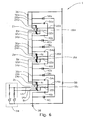
- Fig. 6 shows a simplified embodiment of the high voltage apparatus 1 wherein the voltage multipliers are left out, as the first condensers 40 1 , 40 2 , 40 3 and the fourth condensers 54 may be constituted by the internal capacitance of the high voltage windings 16 1 , 16 2 , 16 3 .
- the high voltage apparatuses 1 in fig. 3 and 4 give a positive output voltage. If all diodes are turned, a negative output voltage is given off.
Landscapes
- Engineering & Computer Science (AREA)
- Power Engineering (AREA)
- Coils Of Transformers For General Uses (AREA)
- Coils Or Transformers For Communication (AREA)
Priority Applications (1)
| Application Number | Priority Date | Filing Date | Title |
|---|---|---|---|
| PL10707367T PL2409309T3 (pl) | 2009-02-23 | 2010-02-22 | Transformator wysokiego napięcia |
Applications Claiming Priority (2)
| Application Number | Priority Date | Filing Date | Title |
|---|---|---|---|
| NO20090825A NO329698B1 (no) | 2009-02-23 | 2009-02-23 | Hoyspenttransformator |
| PCT/NO2010/000069 WO2010095955A1 (en) | 2009-02-23 | 2010-02-22 | High voltage transformer |
Publications (2)
| Publication Number | Publication Date |
|---|---|
| EP2409309A1 EP2409309A1 (en) | 2012-01-25 |
| EP2409309B1 true EP2409309B1 (en) | 2013-09-11 |
Family
ID=42211767
Family Applications (1)
| Application Number | Title | Priority Date | Filing Date |
|---|---|---|---|
| EP10707367.8A Not-in-force EP2409309B1 (en) | 2009-02-23 | 2010-02-22 | High voltage transformer |
Country Status (12)
| Country | Link |
|---|---|
| US (1) | US9490065B2 (sr) |
| EP (1) | EP2409309B1 (sr) |
| CN (1) | CN102362322B (sr) |
| BR (1) | BRPI1009767A2 (sr) |
| CA (1) | CA2752486A1 (sr) |
| DK (1) | DK2409309T3 (sr) |
| ES (1) | ES2438715T3 (sr) |
| NO (1) | NO329698B1 (sr) |
| PL (1) | PL2409309T3 (sr) |
| RS (1) | RS53200B (sr) |
| RU (1) | RU2524672C2 (sr) |
| WO (1) | WO2010095955A1 (sr) |
Families Citing this family (7)
| Publication number | Priority date | Publication date | Assignee | Title |
|---|---|---|---|---|
| EP2740130B1 (en) * | 2011-08-01 | 2015-07-01 | Alstom Technology Ltd | Current limiter |
| TWI438796B (zh) * | 2011-09-29 | 2014-05-21 | Fsp Technology Inc | 變壓器與變壓器的製造方法 |
| EP3563646B1 (en) * | 2016-12-30 | 2025-06-11 | Eagle Harbor Technologies, Inc. | High voltage inductive adder |
| US11181588B2 (en) * | 2018-08-13 | 2021-11-23 | Carlisle Fluid Technologies, Inc. | Systems and methods for detection and configuration of spray system components |
| EP4010910A4 (en) * | 2019-08-05 | 2023-08-16 | Thermo Scientific Portable Analytical Instruments Inc. | POT TRANSFORMER WITH MAGNETIC SHUNT |
| US11873715B2 (en) | 2021-11-04 | 2024-01-16 | Halliburton Energy Services, Inc. | Pulse power drilling assembly transformer with a core having a non-conductive material |
| CN115132463B (zh) * | 2022-08-08 | 2024-07-12 | 常州华迪特种变压器有限公司 | 一种干式电力变压器 |
Family Cites Families (23)
| Publication number | Priority date | Publication date | Assignee | Title |
|---|---|---|---|---|
| US1680910A (en) | 1925-06-09 | 1928-08-14 | Pfiffner Emil | Earthing choking coil or voltage transformer for high voltages |
| US1874563A (en) * | 1925-09-25 | 1932-08-30 | American Telephone & Telegraph | System for producing high voltage direct currents |
| US2570701A (en) * | 1942-03-31 | 1951-10-09 | Martin Marie-Therese | Harmonic-selecting apparatus |
| US3419837A (en) * | 1964-12-09 | 1968-12-31 | Dresser Ind | Pulse transformer |
| US3448340A (en) * | 1965-06-29 | 1969-06-03 | Wagner Electric Corp | Transformer |
| US3360754A (en) * | 1965-06-29 | 1967-12-26 | Wagner Electric Corp | Transformer having reduced differential impedances between secondary portions |
| US3579165A (en) * | 1969-09-24 | 1971-05-18 | Gen Electric | Winding connection for single phase two leg electric transformer |
| US3579078A (en) | 1969-10-06 | 1971-05-18 | Trw Inc | Constant current high-voltage power supply |
| GB1271635A (en) | 1970-01-08 | 1972-04-19 | Ferranti Ltd | Improvements relating to transformers |
| US3675174A (en) * | 1970-11-09 | 1972-07-04 | Electronic Associates | Electrical coil and method of manufacturing same |
| US3675175A (en) | 1971-05-10 | 1972-07-04 | Gen Electric | High voltage coil assembly for electric induction apparatus |
| US4023091A (en) * | 1973-04-04 | 1977-05-10 | Toshio Fujita | Apparatus for detecting axial displacements in power windings of electric induction machines |
| US4270111A (en) * | 1980-02-25 | 1981-05-26 | Westinghouse Electric Corp. | Electrical inductive apparatus |
| US4518941A (en) | 1983-11-16 | 1985-05-21 | Nihon Kohden Corporation | Pulse transformer for switching power supplies |
| US5216356A (en) * | 1990-11-13 | 1993-06-01 | Southwest Electric Company | Shielded three phase transformer with tertiary winding |
| US5847518A (en) * | 1996-07-08 | 1998-12-08 | Hitachi Ferrite Electronics, Ltd. | High voltage transformer with secondary coil windings on opposing bobbins |
| US5912553A (en) * | 1997-01-17 | 1999-06-15 | Schott Corporation | Alternating current ferroresonant transformer with low harmonic distortion |
| IL126748A0 (en) * | 1998-10-26 | 1999-08-17 | Amt Ltd | Three-phase transformer and method for manufacturing same |
| ES2151443B1 (es) * | 1999-01-18 | 2001-07-01 | Es De Electromedicina Y Calida | Transformador de alta tension. |
| DE10117847C1 (de) * | 2001-04-04 | 2003-02-06 | Siemens Ag | Transformator mit forcierter Flüssigkeitskühlung |
| CN2648566Y (zh) | 2003-09-28 | 2004-10-13 | 潘永岐 | 串级式高压脉冲变压器 |
| WO2007045275A1 (en) * | 2005-10-18 | 2007-04-26 | Tte Germany Gmbh | Switched-mode power supply arrangement |
| JP5103728B2 (ja) | 2005-11-24 | 2012-12-19 | ウシオ電機株式会社 | 放電ランプ点灯装置 |
-
2009
- 2009-02-23 NO NO20090825A patent/NO329698B1/no unknown
-
2010
- 2010-02-22 CN CN201080013698.0A patent/CN102362322B/zh not_active Expired - Fee Related
- 2010-02-22 CA CA2752486A patent/CA2752486A1/en not_active Abandoned
- 2010-02-22 ES ES10707367.8T patent/ES2438715T3/es active Active
- 2010-02-22 WO PCT/NO2010/000069 patent/WO2010095955A1/en not_active Ceased
- 2010-02-22 BR BRPI1009767A patent/BRPI1009767A2/pt not_active IP Right Cessation
- 2010-02-22 EP EP10707367.8A patent/EP2409309B1/en not_active Not-in-force
- 2010-02-22 RS RS20130541A patent/RS53200B/sr unknown
- 2010-02-22 DK DK10707367.8T patent/DK2409309T3/da active
- 2010-02-22 RU RU2011133922/07A patent/RU2524672C2/ru not_active IP Right Cessation
- 2010-02-22 PL PL10707367T patent/PL2409309T3/pl unknown
- 2010-02-22 US US13/148,710 patent/US9490065B2/en active Active
Also Published As
| Publication number | Publication date |
|---|---|
| US9490065B2 (en) | 2016-11-08 |
| RU2524672C2 (ru) | 2014-08-10 |
| US20120007706A1 (en) | 2012-01-12 |
| CN102362322B (zh) | 2015-08-26 |
| ES2438715T3 (es) | 2014-01-20 |
| NO20090825L (no) | 2010-08-24 |
| CA2752486A1 (en) | 2010-08-26 |
| EP2409309A1 (en) | 2012-01-25 |
| RS53200B (sr) | 2014-06-30 |
| DK2409309T3 (da) | 2013-12-16 |
| NO329698B1 (no) | 2010-12-06 |
| PL2409309T3 (pl) | 2014-04-30 |
| WO2010095955A1 (en) | 2010-08-26 |
| RU2011133922A (ru) | 2013-03-27 |
| CN102362322A (zh) | 2012-02-22 |
| BRPI1009767A2 (pt) | 2016-03-15 |
Similar Documents
| Publication | Publication Date | Title |
|---|---|---|
| EP2409309B1 (en) | High voltage transformer | |
| US12125631B2 (en) | Shielded electrical transformer | |
| US7903432B2 (en) | High-voltage power generation system and package | |
| JP5813320B2 (ja) | 高電圧用途のための高周波変圧器 | |
| US7193496B2 (en) | Magnetic element and power supply | |
| JP2006007313A5 (sr) | ||
| CN104025213A (zh) | 电感性组件和使用 | |
| US20060049903A1 (en) | Pulse type transformer with increased coupling coefficient through configuration of plural primary windings | |
| JP2012135112A (ja) | 高電圧インバータ装置及びその出力電圧調整方法 | |
| US11222744B1 (en) | Power-dense bipolar high-voltage capacitor charger | |
| CN104426382A (zh) | 变压器 | |
| US20130223109A1 (en) | Small size power supply | |
| US6100781A (en) | High leakage inductance transformer | |
| US9072155B2 (en) | Transformer network | |
| EP2445097A1 (en) | A converter and an electronic equipment provided with such a converter | |
| US9136054B1 (en) | Reduced leakage inductance transformer and winding methods | |
| US7528692B2 (en) | Voltage stress reduction in magnetics using high resistivity materials | |
| JP4343891B2 (ja) | コイル、トランスおよびスイッチング電源 | |
| JP5824862B2 (ja) | 高電圧インバータ装置 | |
| US20170294829A1 (en) | Transformer | |
| WO2016071123A1 (en) | Resonant converter | |
| Kim et al. | Development of a high frequency and high-voltage pulse transformer for a TWT HVPS | |
| AU613211B2 (en) | High frequency matrix transformer | |
| Forsyth et al. | Ultralow-inductance, multielement transformer-rectifier |
Legal Events
| Date | Code | Title | Description |
|---|---|---|---|
| PUAI | Public reference made under article 153(3) epc to a published international application that has entered the european phase |
Free format text: ORIGINAL CODE: 0009012 |
|
| 17P | Request for examination filed |
Effective date: 20110810 |
|
| AK | Designated contracting states |
Kind code of ref document: A1 Designated state(s): AT BE BG CH CY CZ DE DK EE ES FI FR GB GR HR HU IE IS IT LI LT LU LV MC MK MT NL NO PL PT RO SE SI SK SM TR |
|
| DAX | Request for extension of the european patent (deleted) | ||
| GRAP | Despatch of communication of intention to grant a patent |
Free format text: ORIGINAL CODE: EPIDOSNIGR1 |
|
| RAP1 | Party data changed (applicant data changed or rights of an application transferred) |
Owner name: ZAPTEC IP AS |
|
| INTG | Intention to grant announced |
Effective date: 20130403 |
|
| GRAS | Grant fee paid |
Free format text: ORIGINAL CODE: EPIDOSNIGR3 |
|
| GRAA | (expected) grant |
Free format text: ORIGINAL CODE: 0009210 |
|
| AK | Designated contracting states |
Kind code of ref document: B1 Designated state(s): AT BE BG CH CY CZ DE DK EE ES FI FR GB GR HR HU IE IS IT LI LT LU LV MC MK MT NL NO PL PT RO SE SI SK SM TR |
|
| REG | Reference to a national code |
Ref country code: GB Ref legal event code: FG4D |
|
| REG | Reference to a national code |
Ref country code: CH Ref legal event code: EP |
|
| REG | Reference to a national code |
Ref country code: AT Ref legal event code: REF Ref document number: 632029 Country of ref document: AT Kind code of ref document: T Effective date: 20130915 |
|
| REG | Reference to a national code |
Ref country code: IE Ref legal event code: FG4D |
|
| REG | Reference to a national code |
Ref country code: DE Ref legal event code: R096 Ref document number: 602010010191 Country of ref document: DE Effective date: 20131107 |
|
| REG | Reference to a national code |
Ref country code: DK Ref legal event code: T3 Effective date: 20131212 |
|
| REG | Reference to a national code |
Ref country code: NL Ref legal event code: T3 |
|
| REG | Reference to a national code |
Ref country code: SE Ref legal event code: TRGR |
|
| REG | Reference to a national code |
Ref country code: ES Ref legal event code: FG2A Ref document number: 2438715 Country of ref document: ES Kind code of ref document: T3 Effective date: 20140120 |
|
| PG25 | Lapsed in a contracting state [announced via postgrant information from national office to epo] |
Ref country code: HR Free format text: LAPSE BECAUSE OF FAILURE TO SUBMIT A TRANSLATION OF THE DESCRIPTION OR TO PAY THE FEE WITHIN THE PRESCRIBED TIME-LIMIT Effective date: 20130911 Ref country code: CY Free format text: LAPSE BECAUSE OF FAILURE TO SUBMIT A TRANSLATION OF THE DESCRIPTION OR TO PAY THE FEE WITHIN THE PRESCRIBED TIME-LIMIT Effective date: 20130807 Ref country code: LT Free format text: LAPSE BECAUSE OF FAILURE TO SUBMIT A TRANSLATION OF THE DESCRIPTION OR TO PAY THE FEE WITHIN THE PRESCRIBED TIME-LIMIT Effective date: 20130911 Ref country code: NO Free format text: LAPSE BECAUSE OF FAILURE TO SUBMIT A TRANSLATION OF THE DESCRIPTION OR TO PAY THE FEE WITHIN THE PRESCRIBED TIME-LIMIT Effective date: 20131211 |
|
| REG | Reference to a national code |
Ref country code: AT Ref legal event code: MK05 Ref document number: 632029 Country of ref document: AT Kind code of ref document: T Effective date: 20130911 |
|
| REG | Reference to a national code |
Ref country code: LT Ref legal event code: MG4D |
|
| PG25 | Lapsed in a contracting state [announced via postgrant information from national office to epo] |
Ref country code: SI Free format text: LAPSE BECAUSE OF FAILURE TO SUBMIT A TRANSLATION OF THE DESCRIPTION OR TO PAY THE FEE WITHIN THE PRESCRIBED TIME-LIMIT Effective date: 20130911 Ref country code: GR Free format text: LAPSE BECAUSE OF FAILURE TO SUBMIT A TRANSLATION OF THE DESCRIPTION OR TO PAY THE FEE WITHIN THE PRESCRIBED TIME-LIMIT Effective date: 20131212 Ref country code: LV Free format text: LAPSE BECAUSE OF FAILURE TO SUBMIT A TRANSLATION OF THE DESCRIPTION OR TO PAY THE FEE WITHIN THE PRESCRIBED TIME-LIMIT Effective date: 20130911 |
|
| PG25 | Lapsed in a contracting state [announced via postgrant information from national office to epo] |
Ref country code: BE Free format text: LAPSE BECAUSE OF FAILURE TO SUBMIT A TRANSLATION OF THE DESCRIPTION OR TO PAY THE FEE WITHIN THE PRESCRIBED TIME-LIMIT Effective date: 20130911 Ref country code: CY Free format text: LAPSE BECAUSE OF FAILURE TO SUBMIT A TRANSLATION OF THE DESCRIPTION OR TO PAY THE FEE WITHIN THE PRESCRIBED TIME-LIMIT Effective date: 20130911 |
|
| PG25 | Lapsed in a contracting state [announced via postgrant information from national office to epo] |
Ref country code: RO Free format text: LAPSE BECAUSE OF FAILURE TO SUBMIT A TRANSLATION OF THE DESCRIPTION OR TO PAY THE FEE WITHIN THE PRESCRIBED TIME-LIMIT Effective date: 20130911 Ref country code: EE Free format text: LAPSE BECAUSE OF FAILURE TO SUBMIT A TRANSLATION OF THE DESCRIPTION OR TO PAY THE FEE WITHIN THE PRESCRIBED TIME-LIMIT Effective date: 20130911 Ref country code: SK Free format text: LAPSE BECAUSE OF FAILURE TO SUBMIT A TRANSLATION OF THE DESCRIPTION OR TO PAY THE FEE WITHIN THE PRESCRIBED TIME-LIMIT Effective date: 20130911 Ref country code: CZ Free format text: LAPSE BECAUSE OF FAILURE TO SUBMIT A TRANSLATION OF THE DESCRIPTION OR TO PAY THE FEE WITHIN THE PRESCRIBED TIME-LIMIT Effective date: 20130911 Ref country code: IS Free format text: LAPSE BECAUSE OF FAILURE TO SUBMIT A TRANSLATION OF THE DESCRIPTION OR TO PAY THE FEE WITHIN THE PRESCRIBED TIME-LIMIT Effective date: 20140111 |
|
| REG | Reference to a national code |
Ref country code: PL Ref legal event code: T3 |
|
| PG25 | Lapsed in a contracting state [announced via postgrant information from national office to epo] |
Ref country code: AT Free format text: LAPSE BECAUSE OF FAILURE TO SUBMIT A TRANSLATION OF THE DESCRIPTION OR TO PAY THE FEE WITHIN THE PRESCRIBED TIME-LIMIT Effective date: 20130911 |
|
| REG | Reference to a national code |
Ref country code: DE Ref legal event code: R097 Ref document number: 602010010191 Country of ref document: DE |
|
| PG25 | Lapsed in a contracting state [announced via postgrant information from national office to epo] |
Ref country code: PT Free format text: LAPSE BECAUSE OF FAILURE TO SUBMIT A TRANSLATION OF THE DESCRIPTION OR TO PAY THE FEE WITHIN THE PRESCRIBED TIME-LIMIT Effective date: 20140113 |
|
| PLBE | No opposition filed within time limit |
Free format text: ORIGINAL CODE: 0009261 |
|
| STAA | Information on the status of an ep patent application or granted ep patent |
Free format text: STATUS: NO OPPOSITION FILED WITHIN TIME LIMIT |
|
| 26N | No opposition filed |
Effective date: 20140612 |
|
| REG | Reference to a national code |
Ref country code: DE Ref legal event code: R097 Ref document number: 602010010191 Country of ref document: DE Effective date: 20140612 |
|
| PG25 | Lapsed in a contracting state [announced via postgrant information from national office to epo] |
Ref country code: LU Free format text: LAPSE BECAUSE OF FAILURE TO SUBMIT A TRANSLATION OF THE DESCRIPTION OR TO PAY THE FEE WITHIN THE PRESCRIBED TIME-LIMIT Effective date: 20140222 Ref country code: MC Free format text: LAPSE BECAUSE OF FAILURE TO SUBMIT A TRANSLATION OF THE DESCRIPTION OR TO PAY THE FEE WITHIN THE PRESCRIBED TIME-LIMIT Effective date: 20130911 |
|
| REG | Reference to a national code |
Ref country code: IE Ref legal event code: MM4A |
|
| PG25 | Lapsed in a contracting state [announced via postgrant information from national office to epo] |
Ref country code: IE Free format text: LAPSE BECAUSE OF NON-PAYMENT OF DUE FEES Effective date: 20140222 |
|
| REG | Reference to a national code |
Ref country code: FR Ref legal event code: PLFP Year of fee payment: 7 |
|
| PG25 | Lapsed in a contracting state [announced via postgrant information from national office to epo] |
Ref country code: MT Free format text: LAPSE BECAUSE OF FAILURE TO SUBMIT A TRANSLATION OF THE DESCRIPTION OR TO PAY THE FEE WITHIN THE PRESCRIBED TIME-LIMIT Effective date: 20130911 |
|
| PG25 | Lapsed in a contracting state [announced via postgrant information from national office to epo] |
Ref country code: SM Free format text: LAPSE BECAUSE OF FAILURE TO SUBMIT A TRANSLATION OF THE DESCRIPTION OR TO PAY THE FEE WITHIN THE PRESCRIBED TIME-LIMIT Effective date: 20130911 |
|
| PG25 | Lapsed in a contracting state [announced via postgrant information from national office to epo] |
Ref country code: BG Free format text: LAPSE BECAUSE OF FAILURE TO SUBMIT A TRANSLATION OF THE DESCRIPTION OR TO PAY THE FEE WITHIN THE PRESCRIBED TIME-LIMIT Effective date: 20130911 |
|
| PG25 | Lapsed in a contracting state [announced via postgrant information from national office to epo] |
Ref country code: TR Free format text: LAPSE BECAUSE OF FAILURE TO SUBMIT A TRANSLATION OF THE DESCRIPTION OR TO PAY THE FEE WITHIN THE PRESCRIBED TIME-LIMIT Effective date: 20130911 Ref country code: HU Free format text: LAPSE BECAUSE OF FAILURE TO SUBMIT A TRANSLATION OF THE DESCRIPTION OR TO PAY THE FEE WITHIN THE PRESCRIBED TIME-LIMIT; INVALID AB INITIO Effective date: 20100222 |
|
| REG | Reference to a national code |
Ref country code: FR Ref legal event code: PLFP Year of fee payment: 8 |
|
| PGFP | Annual fee paid to national office [announced via postgrant information from national office to epo] |
Ref country code: FI Payment date: 20170213 Year of fee payment: 8 Ref country code: SE Payment date: 20170216 Year of fee payment: 8 Ref country code: DE Payment date: 20170217 Year of fee payment: 8 Ref country code: FR Payment date: 20170217 Year of fee payment: 8 Ref country code: CH Payment date: 20170217 Year of fee payment: 8 |
|
| PGFP | Annual fee paid to national office [announced via postgrant information from national office to epo] |
Ref country code: DK Payment date: 20170216 Year of fee payment: 8 Ref country code: GB Payment date: 20170216 Year of fee payment: 8 Ref country code: PL Payment date: 20170123 Year of fee payment: 8 Ref country code: NL Payment date: 20170216 Year of fee payment: 8 |
|
| PGFP | Annual fee paid to national office [announced via postgrant information from national office to epo] |
Ref country code: IT Payment date: 20170221 Year of fee payment: 8 Ref country code: ES Payment date: 20170213 Year of fee payment: 8 |
|
| PG25 | Lapsed in a contracting state [announced via postgrant information from national office to epo] |
Ref country code: MK Free format text: LAPSE BECAUSE OF FAILURE TO SUBMIT A TRANSLATION OF THE DESCRIPTION OR TO PAY THE FEE WITHIN THE PRESCRIBED TIME-LIMIT Effective date: 20130911 |
|
| REG | Reference to a national code |
Ref country code: DE Ref legal event code: R119 Ref document number: 602010010191 Country of ref document: DE |
|
| REG | Reference to a national code |
Ref country code: CH Ref legal event code: PL |
|
| REG | Reference to a national code |
Ref country code: DK Ref legal event code: EBP Effective date: 20180228 |
|
| REG | Reference to a national code |
Ref country code: SE Ref legal event code: EUG |
|
| REG | Reference to a national code |
Ref country code: NL Ref legal event code: MM Effective date: 20180301 |
|
| GBPC | Gb: european patent ceased through non-payment of renewal fee |
Effective date: 20180222 |
|
| PG25 | Lapsed in a contracting state [announced via postgrant information from national office to epo] |
Ref country code: FI Free format text: LAPSE BECAUSE OF NON-PAYMENT OF DUE FEES Effective date: 20180222 Ref country code: SE Free format text: LAPSE BECAUSE OF NON-PAYMENT OF DUE FEES Effective date: 20180223 |
|
| PG25 | Lapsed in a contracting state [announced via postgrant information from national office to epo] |
Ref country code: LI Free format text: LAPSE BECAUSE OF NON-PAYMENT OF DUE FEES Effective date: 20180228 Ref country code: CH Free format text: LAPSE BECAUSE OF NON-PAYMENT OF DUE FEES Effective date: 20180228 |
|
| REG | Reference to a national code |
Ref country code: FR Ref legal event code: ST Effective date: 20181031 |
|
| PG25 | Lapsed in a contracting state [announced via postgrant information from national office to epo] |
Ref country code: NL Free format text: LAPSE BECAUSE OF NON-PAYMENT OF DUE FEES Effective date: 20180301 |
|
| PG25 | Lapsed in a contracting state [announced via postgrant information from national office to epo] |
Ref country code: DE Free format text: LAPSE BECAUSE OF NON-PAYMENT OF DUE FEES Effective date: 20180901 Ref country code: DK Free format text: LAPSE BECAUSE OF NON-PAYMENT OF DUE FEES Effective date: 20180228 |
|
| PG25 | Lapsed in a contracting state [announced via postgrant information from national office to epo] |
Ref country code: GB Free format text: LAPSE BECAUSE OF NON-PAYMENT OF DUE FEES Effective date: 20180222 Ref country code: IT Free format text: LAPSE BECAUSE OF NON-PAYMENT OF DUE FEES Effective date: 20180222 Ref country code: FR Free format text: LAPSE BECAUSE OF NON-PAYMENT OF DUE FEES Effective date: 20180228 |
|
| REG | Reference to a national code |
Ref country code: ES Ref legal event code: FD2A Effective date: 20190801 |
|
| PG25 | Lapsed in a contracting state [announced via postgrant information from national office to epo] |
Ref country code: ES Free format text: LAPSE BECAUSE OF NON-PAYMENT OF DUE FEES Effective date: 20180223 |
|
| PG25 | Lapsed in a contracting state [announced via postgrant information from national office to epo] |
Ref country code: PL Free format text: LAPSE BECAUSE OF NON-PAYMENT OF DUE FEES Effective date: 20180222 |