EP2407976A2 - Nichtflüchtige wiederprogrammierbare Speichervorrichtung - Google Patents
Nichtflüchtige wiederprogrammierbare Speichervorrichtung Download PDFInfo
- Publication number
- EP2407976A2 EP2407976A2 EP11173262A EP11173262A EP2407976A2 EP 2407976 A2 EP2407976 A2 EP 2407976A2 EP 11173262 A EP11173262 A EP 11173262A EP 11173262 A EP11173262 A EP 11173262A EP 2407976 A2 EP2407976 A2 EP 2407976A2
- Authority
- EP
- European Patent Office
- Prior art keywords
- resistor
- sicr
- memory cell
- resistance
- memory device
- Prior art date
- Legal status (The legal status is an assumption and is not a legal conclusion. Google has not performed a legal analysis and makes no representation as to the accuracy of the status listed.)
- Granted
Links
- 230000015654 memory Effects 0.000 claims abstract description 123
- 230000005012 migration Effects 0.000 claims abstract description 56
- 238000013508 migration Methods 0.000 claims abstract description 56
- 230000004044 response Effects 0.000 claims abstract description 16
- 238000000034 method Methods 0.000 claims description 31
- 239000000463 material Substances 0.000 claims description 29
- 230000002411 adverse Effects 0.000 claims description 18
- 239000004065 semiconductor Substances 0.000 claims description 18
- 239000000758 substrate Substances 0.000 claims description 18
- 230000005684 electric field Effects 0.000 claims description 12
- 230000000694 effects Effects 0.000 claims description 7
- 238000010438 heat treatment Methods 0.000 claims description 5
- 238000009877 rendering Methods 0.000 claims description 2
- 230000008859 change Effects 0.000 abstract description 33
- 230000008569 process Effects 0.000 description 18
- 239000002184 metal Substances 0.000 description 15
- 229910052751 metal Inorganic materials 0.000 description 15
- 239000010409 thin film Substances 0.000 description 12
- 239000003989 dielectric material Substances 0.000 description 11
- 239000010949 copper Substances 0.000 description 10
- 239000010408 film Substances 0.000 description 10
- 238000004519 manufacturing process Methods 0.000 description 5
- 229910052710 silicon Inorganic materials 0.000 description 5
- QVGXLLKOCUKJST-UHFFFAOYSA-N atomic oxygen Chemical compound [O] QVGXLLKOCUKJST-UHFFFAOYSA-N 0.000 description 4
- 150000001875 compounds Chemical class 0.000 description 4
- 230000007423 decrease Effects 0.000 description 4
- 238000001514 detection method Methods 0.000 description 4
- 239000001301 oxygen Substances 0.000 description 4
- 229910052760 oxygen Inorganic materials 0.000 description 4
- 230000002441 reversible effect Effects 0.000 description 4
- 229910001218 Gallium arsenide Inorganic materials 0.000 description 3
- VYPSYNLAJGMNEJ-UHFFFAOYSA-N Silicium dioxide Chemical compound O=[Si]=O VYPSYNLAJGMNEJ-UHFFFAOYSA-N 0.000 description 3
- XUIMIQQOPSSXEZ-UHFFFAOYSA-N Silicon Chemical compound [Si] XUIMIQQOPSSXEZ-UHFFFAOYSA-N 0.000 description 3
- 238000003491 array Methods 0.000 description 3
- 239000011651 chromium Substances 0.000 description 3
- 239000002019 doping agent Substances 0.000 description 3
- 238000005516 engineering process Methods 0.000 description 3
- 239000000203 mixture Substances 0.000 description 3
- 230000005855 radiation Effects 0.000 description 3
- 239000010703 silicon Substances 0.000 description 3
- HBMJWWWQQXIZIP-UHFFFAOYSA-N silicon carbide Chemical compound [Si+]#[C-] HBMJWWWQQXIZIP-UHFFFAOYSA-N 0.000 description 3
- 229910010271 silicon carbide Inorganic materials 0.000 description 3
- -1 SiCr Inorganic materials 0.000 description 2
- 229910045601 alloy Inorganic materials 0.000 description 2
- 239000000956 alloy Substances 0.000 description 2
- 229910052804 chromium Inorganic materials 0.000 description 2
- 230000001747 exhibiting effect Effects 0.000 description 2
- 150000002500 ions Chemical class 0.000 description 2
- 238000012986 modification Methods 0.000 description 2
- 230000004048 modification Effects 0.000 description 2
- 238000012545 processing Methods 0.000 description 2
- 229910052814 silicon oxide Inorganic materials 0.000 description 2
- 238000004544 sputter deposition Methods 0.000 description 2
- 238000007725 thermal activation Methods 0.000 description 2
- RYGMFSIKBFXOCR-UHFFFAOYSA-N Copper Chemical compound [Cu] RYGMFSIKBFXOCR-UHFFFAOYSA-N 0.000 description 1
- 229910007243 Si2Cr Inorganic materials 0.000 description 1
- 229910052581 Si3N4 Inorganic materials 0.000 description 1
- BLRPTPMANUNPDV-UHFFFAOYSA-N Silane Chemical compound [SiH4] BLRPTPMANUNPDV-UHFFFAOYSA-N 0.000 description 1
- BOTDANWDWHJENH-UHFFFAOYSA-N Tetraethyl orthosilicate Chemical compound CCO[Si](OCC)(OCC)OCC BOTDANWDWHJENH-UHFFFAOYSA-N 0.000 description 1
- 230000001133 acceleration Effects 0.000 description 1
- 238000013459 approach Methods 0.000 description 1
- DYRBFMPPJATHRF-UHFFFAOYSA-N chromium silicon Chemical compound [Si].[Cr] DYRBFMPPJATHRF-UHFFFAOYSA-N 0.000 description 1
- 229910052681 coesite Inorganic materials 0.000 description 1
- 230000000295 complement effect Effects 0.000 description 1
- 229910052802 copper Inorganic materials 0.000 description 1
- 229910052906 cristobalite Inorganic materials 0.000 description 1
- 230000003247 decreasing effect Effects 0.000 description 1
- 238000010586 diagram Methods 0.000 description 1
- 230000004069 differentiation Effects 0.000 description 1
- 239000007789 gas Substances 0.000 description 1
- 239000012535 impurity Substances 0.000 description 1
- 150000004767 nitrides Chemical class 0.000 description 1
- 238000013021 overheating Methods 0.000 description 1
- 125000004430 oxygen atom Chemical group O* 0.000 description 1
- 239000002245 particle Substances 0.000 description 1
- 238000007747 plating Methods 0.000 description 1
- 239000002243 precursor Substances 0.000 description 1
- 230000002035 prolonged effect Effects 0.000 description 1
- 230000009467 reduction Effects 0.000 description 1
- 230000035939 shock Effects 0.000 description 1
- 239000000377 silicon dioxide Substances 0.000 description 1
- HQVNEWCFYHHQES-UHFFFAOYSA-N silicon nitride Chemical compound N12[Si]34N5[Si]62N3[Si]51N64 HQVNEWCFYHHQES-UHFFFAOYSA-N 0.000 description 1
- 229910052682 stishovite Inorganic materials 0.000 description 1
- 239000000126 substance Substances 0.000 description 1
- 229910052905 tridymite Inorganic materials 0.000 description 1
- WFKWXMTUELFFGS-UHFFFAOYSA-N tungsten Chemical compound [W] WFKWXMTUELFFGS-UHFFFAOYSA-N 0.000 description 1
- 229910052721 tungsten Inorganic materials 0.000 description 1
- 239000010937 tungsten Substances 0.000 description 1
Images

Classifications
-
- G—PHYSICS
- G11—INFORMATION STORAGE
- G11C—STATIC STORES
- G11C13/00—Digital stores characterised by the use of storage elements not covered by groups G11C11/00, G11C23/00, or G11C25/00
- G11C13/0002—Digital stores characterised by the use of storage elements not covered by groups G11C11/00, G11C23/00, or G11C25/00 using resistive RAM [RRAM] elements
- G11C13/0007—Digital stores characterised by the use of storage elements not covered by groups G11C11/00, G11C23/00, or G11C25/00 using resistive RAM [RRAM] elements comprising metal oxide memory material, e.g. perovskites
-
- G—PHYSICS
- G11—INFORMATION STORAGE
- G11C—STATIC STORES
- G11C13/00—Digital stores characterised by the use of storage elements not covered by groups G11C11/00, G11C23/00, or G11C25/00
- G11C13/0002—Digital stores characterised by the use of storage elements not covered by groups G11C11/00, G11C23/00, or G11C25/00 using resistive RAM [RRAM] elements
- G11C13/0021—Auxiliary circuits
- G11C13/0059—Security or protection circuits or methods
-
- G—PHYSICS
- G11—INFORMATION STORAGE
- G11C—STATIC STORES
- G11C7/00—Arrangements for writing information into, or reading information out from, a digital store
- G11C7/04—Arrangements for writing information into, or reading information out from, a digital store with means for avoiding disturbances due to temperature effects
-
- G—PHYSICS
- G11—INFORMATION STORAGE
- G11C—STATIC STORES
- G11C7/00—Arrangements for writing information into, or reading information out from, a digital store
- G11C7/24—Memory cell safety or protection circuits, e.g. arrangements for preventing inadvertent reading or writing; Status cells; Test cells
-
- H—ELECTRICITY
- H10—SEMICONDUCTOR DEVICES; ELECTRIC SOLID-STATE DEVICES NOT OTHERWISE PROVIDED FOR
- H10N—ELECTRIC SOLID-STATE DEVICES NOT OTHERWISE PROVIDED FOR
- H10N70/00—Solid-state devices having no potential barriers, and specially adapted for rectifying, amplifying, oscillating or switching
- H10N70/20—Multistable switching devices, e.g. memristors
- H10N70/24—Multistable switching devices, e.g. memristors based on migration or redistribution of ionic species, e.g. anions, vacancies
-
- H—ELECTRICITY
- H10—SEMICONDUCTOR DEVICES; ELECTRIC SOLID-STATE DEVICES NOT OTHERWISE PROVIDED FOR
- H10N—ELECTRIC SOLID-STATE DEVICES NOT OTHERWISE PROVIDED FOR
- H10N70/00—Solid-state devices having no potential barriers, and specially adapted for rectifying, amplifying, oscillating or switching
- H10N70/801—Constructional details of multistable switching devices
- H10N70/821—Device geometry
- H10N70/823—Device geometry adapted for essentially horizontal current flow, e.g. bridge type devices
-
- H—ELECTRICITY
- H10—SEMICONDUCTOR DEVICES; ELECTRIC SOLID-STATE DEVICES NOT OTHERWISE PROVIDED FOR
- H10N—ELECTRIC SOLID-STATE DEVICES NOT OTHERWISE PROVIDED FOR
- H10N70/00—Solid-state devices having no potential barriers, and specially adapted for rectifying, amplifying, oscillating or switching
- H10N70/801—Constructional details of multistable switching devices
- H10N70/881—Switching materials
Definitions
- Non-volatile re-programmable memory is frequently semiconductor device based, such as used in EEprom or Flash memory.
- each memory cell may include multiple transistors, limiting the reduction in size achievable.
- the transistors are added to the semiconductor during front end processing.
- non-volatile re-programmable memory works on a principle of charging.
- the use of a stored charge limits the environments the memory device can be used in because the charge can leak away quickly at elevated temperatures.
- non-volatile re-programmable memory devices include a resistor that changes resistance through a phase change. These phase change memories are made in the backend of the wafer fabrication process. The materials used are normally of a low molten point and phase change can take place at as low as 150°C. The low temperature of phase change results in difficulty in retaining data at an elevated temperature.
- Particular aspects of the present disclosure relate generally to a re-programmable non-volatile memory device wherein the memory state is related to the resistance level of the memory cell.
- the memory state of the memory cell is changed through a resistance change due to SiCr-facilitated migration.
- SiCr-facilitated migration refers to electrical-field driven migration and/or electromigration, wherein at least one element, possibly other than electromigration ions, migrates along the SiCr resistor.
- a memory device in certain embodiments of the present disclosure, includes a first memory cell-access line terminating at a first node and a second memory cell-access line terminating at a second node.
- the memory device includes a memory cell resistor, made of a resistive material exhibiting reversibly-settable resistive states via SiCr-facilitated migration, and connected to and between each of the first and second nodes.
- the memory cell resistor can be a thin film resistor or a vertical resistor, for example.
- the resistive material is Silicon Chromium (SiCr), includes SiCr, and/or is at least predominantly SiCr.
- a memory device includes a SiCr-based resistor configured to exhibit a first resistance state in response to a write current, and to exhibit a second resistance state in response to an erase current.
- the write and erase currents are of opposite directions and the first and second resistance states are set by SiCr-facilitated migration.
- the memory device includes programming circuitry configured to apply the write and erase currents to set the respective resistance states of the SiCr-based resistor.
- a read circuit is configured to apply a read current to the SiCr-based resistor to facilitate the detection of the resistance state of the resistor, the read current having a value that is insufficient to change the resistance state of the SiCr-based resistor.
- the thermal-activation energy of the SiCr-facilitated migration process is high, for example around 2.5eV.
- a method for protecting the data stored in a memory device includes providing a memory device operatively coupled to control circuitry configured and arranged to access logic states stored within the memory device.
- a signal is generated for protecting the memory device from a potentially environmentally adverse condition involving a high temperature in which the control circuitry is known to fail.
- the control circuitry is rendered in a protect mode that protects the control circuitry from the environmentally adverse condition.
- the logic states stored in the memory device are maintained while subjecting the memory device to the environmentally adverse condition.
- the protect mode is disabled in response to an indication that the environmentally adverse condition has dissipated, allowing the control circuitry to access the logic states stored in the memory device.
- a memory device is a SiCr based resistor connected with interconnect metal lines and surrounded by inter-metal dielectrics on a substrate.
- inter-metal dielectrics are silicon-oxide materials such as those used in integrated circuits.
- the SiCr based resistor is a thin film resistor.
- the SiCr film can be applied to a semiconductor device in the backend of line (BEOL) portion of the wafer fabrication process.
- BEOL backend of line
- the device can be a single device memory cell.
- the memory cell can be integrated with a variety of integrated circuit technologies.
- the SiCr based resistor can be used with silicon or with III-V compounds such as GaAs.
- the present disclosure is believed to be useful for providing a heat and radiation resistant non-volatile re-programmable memory device, and the disclosure has been found to be particularly suited for use in arrangements and methods dealing with integrated circuitry. While the present disclosure is not necessarily limited to such applications, various aspects of the disclosure may be appreciated through a discussion of various examples using these contexts.
- the resistor is made of a SiCr based material.
- a single resistor works as a memory cell, allowing for high density of memories on an integrated circuit.
- a SiCr based resistor can be added to an integrated circuit in the backend portion of the wafer fabrication process. In specific embodiments, this allows for resistors to be layered to allow for 3D memory and increase in memory density.
- a resistor of SiCr based material can reversibly change resistance levels.
- the change in resistance occurs from Si migration in the same direction as the current flow, and the electrical fields.
- the Si migrates because the Si is partially positively ionized.
- small amounts of oxygen present in the SiCr based material migrate in the opposite direction of the current and the migrating Si material, and thus the same direction as the electrons. Such migration can be caused by electromigration or by the electrical field if the oxygen atoms are partially negatively ionized. Both migration processes have been found to be accelerated by high temperatures, due to Joule heating.
- the observed resistance change is a result of the migration of both Si and Oxygen.
- One or both of the material migrations observed therewith can be considered as SiCr-facilitated migration, or electrical-field driven migration and/or electromigration.
- alternative and complementary materials exhibiting reversibly-settable resistive-states via SiCr-facilitated migration include various alloys such as SiCr, Si 2 Cr, SiCr-based materials (optionally) doped with impurities concentrated to effect applications-specific results (including but not limited to altering the electromigration), and other materials that are at least predominantly composed of SiCr and also composed in more substance of other materials to effect applications-specific results and/or alter the manner in which SiCr-facilitated migration would otherwise be set if larger amounts of SiCr or pure SiCr were used as the material.
- the SiCr based material has a composition of 70% Si and 28% Cr, by weight, plus approximately 2% of Oxygen as a dopant and residual gas.
- the dopant is a material other than Oxygen, and the ratio between Si, Cr and dopant varies widely.
- the amount of Cr present in the material can vary from approximately 20% to approximately 33%. Changes in composition of the SiCr-based material are also used to affect and/or control the temperature coefficient of resistance (TCR) of the material.
- a SiCr based thin film resistor is added to a semiconductor device during BEOL. This addition allows for the addition of the SiCr thin film resistor without involving the semiconductor substrate.
- a layer of dielectric material is laid on the substrate.
- the dielectric material is a silicon-oxide related material deposited from various precursors, such as SiH 4 or TEOS.
- the dielectric material is doped or undoped and/or the dielectric material is silicon-nitride, a mixture of oxide and nitride (silicon-oxynitride), or other dielectric material used in the wafer fabrications of the IC industry.
- the SiCr thin film resistor is deposited, using sputtering, for example.
- the resistor is etched to the desired placement.
- a second dielectric layer is deposited, and vias (through holes) are etched into the dielectric layer at points corresponding to the ends of each of the etched resistors.
- a metal interconnect material such as Tungsten or copper is deposited in the etched via, and as a metal interconnect layer. This metal interconnect layer can be etched to connect the resistor as desired.
- the process can be repeated multiple times to lay down a number of SiCr based thin film resistors.
- the SiCr based thin film resistors can be connected to metal interconnect layers above or below the resistor.
- This approach can yield a high density of resistors and therefore high-density memory cells.
- This backend processing can occur at relatively low temperatures, less than 350°C, for example.
- the resistors are added during the backend portion of wafer fabrication, the memory can be integrated with a wide variety of integrated circuit technologies, such as silicon, III-V compounds such as GaAs, or other semiconductor compounds such as silicon carbide.
- the BEOL process is based on Cu-based interconnect technologies.
- the BEOL process is a "duel damascene process.”
- a dielectric material is laid on the substrate.
- the dielectric used can be low-K or ultra low-k dielectric, made mainly of p-SiO 2 , SiOC, SiCOH or other materials.
- the SiCr film is deposited, using sputtering for example.
- the resistive film is patterned to the desired placement.
- the next dielectric layer is deposited. Vias (through holes) connecting the SiCr resistors with a Cu interconnect above it are formed. Trenches for the Cu interconnects are formed on the surface of the dielectric layer.
- Cu is deposited in the via holes and the trenches using Cu plating followed by Cu CMP.
- a cap layer of dielectric material is formed over the Cu interconnects. The process can be repeated to achieve multiple layers with SiCr based resistors. In embodiments with more than one resistor layer, holes can be etched to connect either the SiCr resistors above or below a Cu layer to the Cu interconnects.
- a SiCr based resistor of a memory device is programmed with a current (voltage) pulse, and erased with a similar current pulse in the reversed current flow direction.
- the current pulse changes the resistance of the memory device due SiCr-facilitated migration.
- the current pulse can be of a few milliamperes of a few volts in milliseconds.
- the current flow works as the driving force of migration of elements along the SiCr resistor.
- the Joule heating effect of the current accelerates the electrical-field driven migration and/or electromigration processes.
- the SiCr film changes resistivity by 20% or more.
- a positive current pulse decreases the resistivity of the SiCr film.
- applying a current in the opposite direction returns the resistivity of the SiCr film to its original level.
- the resistance of the single resistor is changed due to SiCr-facilitated migration.
- the basic structure of the device is a resistive film connected with metal lines and surrounded by inter-metal dielectrics such as those found in standard integrated circuits.
- a memory device is programmed by changing the resistance of the resistive film. Programming can be done with a current pulse of a few milliamperes of a few volts in milliseconds. The current flow works as the driving force of migration of elements along the film. The Joule heating effect of application of the current accelerates the electrical-field driven migration and/or the electromigration process.
- the application of a current pulse changes (decreases, for example) the resistivity of the thin film resistor by 10%, in other embodiments the resistivity is changed by 20% or 30% or more.
- an erase of the memory device can be achieved when the same or similar current pulse as for the writing step is applied, but in the reverse current direction. During this current pulse the migration element in the programming step migrates back to where it came from, and the resistivity of the thin film resistor returns to its original level. The writing-erase cycle can be repeated again and again. In various embodiments the resistivity change process can be reversed if the current flow direction is reversed.
- current pulse strength and/or duration can be varied.
- a single SiCr-based resistor can store multiple logic states. For example, applying a pulse of a first strength in duration can change the resistivity of the resistor by around 10% from the original resistance level. A second pulse can be applied to the SiCr-based resistor to increase the change in resistivity for the original resistance level by around 20%. The different amount of resistance change can be achieved by a different strength pulse, a different duration pulse, or a combination of both.
- a single strong pulse can change the resistance by around 20% instead of two individual pulses.
- an additional pulse can be applied to increase the change in resistance level to around 30%.
- the difference in resistance levels of approximately 10% allow for differentiation of the logic state stored during the reading process.
- the logic states can be removed/and or leveled down by the application of a current in the opposite direction.
- a single large pulse can be applied to reset the resistance level of the SiCr-based resistor regardless of the final level stored in the memory cell.
- a pulse approximately equal in strength, but in the opposite direction of the last programming pulse, applied to the resistor will reverse the change in resistance level about the same amount as the previous pulse.
- reading of the data stored in the SiCr based resistor is done at a low current.
- the characteristics of the SiCr based material allow for any change of resistivity at a low current level to be minimal compared to the resistance change during the writing step.
- SiCr has a low temperature coefficient of resistance (TCR) that is less than 100 ppm/°C.
- SiCr is also a hard alloy with a molten point above 1300°C. The thermal activation energy and the field/current acceleration effect of the SiCr-facilitated migration process are high.
- the resistive memory device is able to operate at temperatures above 300°C.
- the memory cell is radiation resistive. The cell can maintain its stored logic state in the presence of high energy particles, X-rays, UV-light or visible light, for example.
- the thin film resistor is configured to maintain its resistance state at above 200°C. In other embodiments the resistor maintains its resistance state above 300°C.
- the resistor can be used with a heat resistant substrate, such as silicon carbide. The high temperature resistance allows the resistor to withstand temperature shocks, and may be particularly useful in flash devices.
- a memory device includes a signal generator, a resistor, and programming circuitry.
- the signal generator provides a signal to the programming circuitry to indicate a potentially environmentally adverse condition involving a high temperature in which the programming circuitry is known to fail.
- the programming circuitry includes a circuit to initiate a protect mode in response to a signal from the signal generator.
- the resistor maintains its stored logic state, by maintaining its resistance level, during the protect mode.
- the programming circuitry is unable to access the logic state stored in the resistor during the protect mode.
- a resistor for use in a single cell memory device is disclosed, consistent with an embodiment of the present disclosure.
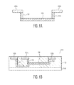
- a SiCr-based resistor 106 is connected at each end to vias 104, which connect metal interconnects 102a to one end of the resistor 106 and metal interconnect 102b to the other end of the resistor 106.
- the resistance level of resistor 106 is changed when a current pulse of sufficient strength is applied to metal interconnect 102a.
- the current pulse has a strength of a few milliamperes of a few volts applied for milliseconds.
- a current pulse of approximately 4 mA at a few volts can be applied for 20-30 milliseconds. In other embodiments a pulse of 1-2 mA and less than several volts can be applied. In various embodiments a voltage pump is used in the application of the pulse. It has been discovered that the application of a strong current pulse to a SiCr-based resistor 106 alters the resistance level of the resistor 106 by 20% or more. The resistance of the SiCr-based resistor 106 is changed through a SiCr-facilitated migration process. A current pulse having the same or similar strength as the first current pulse can be applied to metal interconnect 102b to return the SiCr-based resistor 106 to its original resistance state. The SiCr-facilitated migration process is reversed through the application of a current pulse of the same or similar magnitude in the reverse direction.
- the change in resistance is a decrease in resistance.
- the decrease in resistance of the SiCr-based resistor stays when the current pulse is no longer applied to the SiCr-based resistor.
- the change in resistance results in storage of a logic state.
- a decreased resistance is equivalent to a logic state of 1.
- the logic state stored in the SiCr-based resistor 106 can be read by applying a current much smaller than the current required to change the resistance of the resistor to store the logic state. For example, a read current can be applied at interconnect 102a through vias 104 to one end of SiCr-based resistor 106. The current is received at metal interconnect 102b and provided to an output circuit (not pictured) for receiving the read signal after it has been applied to the SiCr-based resistor 106 and determining the logic state stored in the SiCr-based resistor 106.
- FIG. 1B shows a SiCr-based resistor implemented in an integrated circuit device 100, consistent with an embodiment of the present disclosure.
- the device includes a substrate 108, including a semiconductor and possibly a portion of BEOL layer stack.
- the substrate 108 can be a silicon-based substrate. In other embodiments there can be another semiconductor-based substrate such as silicon carbide or an III-V semiconductor compound such as GaAs.
- the metal interconnects 102, vias 104 and SiCr-based resistor 106 are deposited on the substrate during BEOL. Between the linked interconnects 102, vias 104 and SiCr-based resistors 106 is dielectric material 110. In certain embodiments multiple levels of interconnects 102, as well as multiple levels of SiCr-based resistor 106 can be deposited during the backend process.
- FIG. 2A shows a memory cell 200 having a single transistor 204 and a single resistor 206 forming a memory cell consistent with an embodiment of the present disclosure.
- Resistor 206 can be a thin film resistor or a vertical resistor, for example.
- the transistor 204 has a word line 208 attached to its gate, a source line 210 attached to its source, and the transistor 204's drain is attached to one end of SiCr-based resistor 206. The other end of SiCr-based resistor is attached to a bit line 212.
- the resistance of resistor 206 is changed through SiCr facilitated migration.
- bit line 212 This is achieved by applying a voltage Vprog to bit line 212, setting the word line 208 voltage to high, so the gate of the transistor opens, allowing for current flow, and setting source line 210 to 0V.
- current flows from the bit line 212 through resistor 106 towards 0V at source line 210.
- Inverse programming, or erasing is achieved by setting bit line 212 to 0V, word line 208 is set to a voltage high enough that the gate of the transistors opens, and source line 210 is set to Vprog. Reading of the value stored in the memory cell is achieved by setting bit line 212 to Vread, word line 208 to Vwl-read, and the source line 210 to ground.
- the value of Vprog is the voltage necessary to change the resistance value of the SiCr-based resistor 206 by at least 10%. In certain embodiments the resistance of the SiCr-based resistor 206 is changed up to 30%. In contrast, the voltage Vread is relatively small, and has a low current level.
- Figure 2B depicts four memory cells arranged in a 2X2 NOR memory array 220 consistent with an embodiment of the present disclosure. Each memory cell is arranged in a similar fashion to those illustrated in Figure 2A .
- the programming and inverse programming of each individual memory cell is achieved as described above. In various embodiments and implementations it can be desirable to only program some, but not all, of the interconnected memory cells.
- the bit line 212 is floating or set to 0V for memory cells that are not selected, and/or the word line 208 is set to 0V for non-selected memory cells 200.
- bit line 212 is floating or to Vprog for memory cells 200 that are not selected, and/or the word line 208 is set to 0V for memory cells 200 not selected.
- the bit lines 212a and 212b connect the memory cells 200 of a particular column
- the word lines 208a and 208b connect the memory cells 200 of a particular row. This allows for selection of a memory cell based on its column and row designation. It also allows for the expansion of the array to include more than four memory cells.
- the memory cells are arranged in an AND memory array. In such embodiments (not shown) the array includes two separate source lines, one for each column.
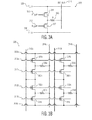
- FIG. 3A depicts a memory cell having a single SiCr-based resistor 306 and two transistors 302 and 304, consistent with an embodiment of the present disclosure.
- the V_ss line 316 is set to ground and the V_pp line 308 is set to Vprog, except during reading of the stored logic state, in which case V_pp is set to Vdd.
- Programming of the memory cell 300 is achieved by setting the P_ gate line 310 of Tp transistor 304 to high as well as the N_gate line 312 of Tn transistor 302 to high. This causes the N gate of transistor 302 to be open while the P gate of the transistor 304 is closed.
- Bit line 314 is set to Vprog. This allows for current to flow from bit line 314, through resistor 306 and towards ground.
- Vprog is chosen to be sufficiently high that the flow of current through resistor 306 causes the resistance of resistor 306 to change by at least 10%, for example.
- the change in resistance to resistor 306 is achieved through SiCr-facilitated migration, and remains when current is not actively flowing through the resistor.
- Inverse programming, or erasing, occurs through a current flow of the same or similar magnitude, but in the reverse direction. This is achieved by setting the N_gate line 312 of transistor 302 and the P_gate line 310 of transistor 304 to low and the Bit line 314 to ground. Setting the transistor gates to low causes the N_gate of transistor 302 to close and the P_gate of transistor 304 to open.
- V_pp 308 is set to Vprog and the bit line 314 current flows from V_pp through transistor 304 and through resistor 306 towards bit line 314, which is the opposite direction of flow through resistor 306.
- the bit line is set to V_b1_read, which is a voltage level lower than Vprog that does not affect the resistance of the resistor 306 to a noticeable level as compared to the application of Vprog.
- V_pp 308, N-gate and P-gate are all set to Vdd.
- the two transistors are different transistors, one an nMOS transistor and one a pMOS transistor.
- Figure 3B depicts an AND memory array 320 made of four memory cells 300 with two transistors and one resistor, consistent with an embodiment of the present disclosure.
- the columns of memory cells are connected both by a bit line 314 and a V_ss line 316.
- the memory cells of each column can be connected by a bit line 314 and a V_pp line 308.
- the memory cells are connected by V_pp lines 308a and 308b.
- the N_gate lines 312a and 312b and P_gates lines 310a and 310b further connect portions of the memory cell along the rows.
- the memory cells 300 can be arranged in a NOR memory array.
- both the V_pp lines and the V_ss lines connect memory cells along rows.
- a single memory cell 300 can be isolated for read/write/or erase procedures due to the column/row connections.
- an array larger than 2X2 can be implemented in various embodiments.
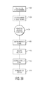
- Figure 4 depicts a method of operating the memory device consistent with an embodiment of the disclosure.
- a memory cell or memory cell array as described above with respect to figures 1-3 for example, is operatively coupled to control circuitry configured and arranged to access logic states stored within the memory device.
- the control circuitry sends a signal to the memory device containing information to be stored.
- the control circuit provides various currents and voltages to the bit lines, word lines, and source lines of the memory array to store various logic states in each memory cell.
- a signal is generated when an environmentally adverse condition is detected. The signal is generated when a condition is detected under which the control circuitry is known to fail.
- step 408 in response to the generated signal, the control circuitry is in a protect mode that protects the control circuitry from the environmentally adverse condition.
- step 410 the logic states stored in the memory device are maintained while the memory device is subjected to an environmentally adverse condition, such as a spike in temperature.
- step 412 the protect mode is disabled once it has been indicated that the environmentally adverse condition has dissipated. This allows the control circuit to access the stored logic states in the memory device.
- step 414 the control circuitry accesses the stored logic states in the memory device. In certain embodiments this is achieved by applying a current significantly smaller than the one used to program the memory cells, to each cell from which information is desired.
- step 414 the memory device is reprogrammed to store new logic states.
- the environmentally adverse condition is a high temperature condition.
- the high temperature condition can be above 200°C. In other embodiments it can be above 250°C or above 300°C.
- the control circuitry is unable to access the stored logic states during protect mode.
- any of the memory arrays can be implemented with appropriate programming circuitry to apply the appropriate voltages to each of the lines in order to change the resistance state of the memory resistor to represent the desired logic state.
- such programming circuitry can be part of a larger control circuit including a reading circuit for determining the value stored in the memory resistor.
- the memory arrays and control circuitry can be used in a variety of applications.
- the memory arrays can be used in applications requiring non-volatile re-programmable memory that will be subject to high temperatures or high levels of radiation.
- the memory device can be used in electronic devices and computers that are prone to overheating.
- the memory device can also be used for field or other equipment routinely stored or used in areas without climate control.
- the memory cell is a single resistor located between a first and second node.
- the resistor stores different resistance states corresponding to different resistance values set by SiCr-facilitated migration.
- the SiCr-facilitated migration occurs in response to energy presented between the first and second nodes.
- the application of a signal to a first node of the memory cell resistor forces the migration of elements along the memory cell resistor to set the resistance value of the memory cell resistor.
- the application of a second signal of approximately equal strength to the second node reverses the change and resistance and returns the memory cell to the previous resistance level.
- the resistor is made of SiCr.
Landscapes
- Engineering & Computer Science (AREA)
- Computer Security & Cryptography (AREA)
- Chemical & Material Sciences (AREA)
- Materials Engineering (AREA)
- Semiconductor Memories (AREA)
Applications Claiming Priority (1)
| Application Number | Priority Date | Filing Date | Title |
|---|---|---|---|
| US12/835,588 US8169811B2 (en) | 2010-07-13 | 2010-07-13 | Non-volatile re-programmable memory device |
Publications (4)
| Publication Number | Publication Date |
|---|---|
| EP2407976A2 true EP2407976A2 (de) | 2012-01-18 |
| EP2407976A3 EP2407976A3 (de) | 2012-03-07 |
| EP2407976A8 EP2407976A8 (de) | 2012-04-18 |
| EP2407976B1 EP2407976B1 (de) | 2017-03-29 |
Family
ID=44645491
Family Applications (1)
| Application Number | Title | Priority Date | Filing Date |
|---|---|---|---|
| EP11173262.4A Not-in-force EP2407976B1 (de) | 2010-07-13 | 2011-07-08 | Nichtflüchtige wiederprogrammierbare Speichervorrichtung |
Country Status (3)
| Country | Link |
|---|---|
| US (1) | US8169811B2 (de) |
| EP (1) | EP2407976B1 (de) |
| CN (1) | CN102332305B (de) |
Families Citing this family (8)
| Publication number | Priority date | Publication date | Assignee | Title |
|---|---|---|---|---|
| US8927909B2 (en) | 2010-10-11 | 2015-01-06 | Stmicroelectronics, Inc. | Closed loop temperature controlled circuit to improve device stability |
| US9159413B2 (en) | 2010-12-29 | 2015-10-13 | Stmicroelectronics Pte Ltd. | Thermo programmable resistor based ROM |
| US8809861B2 (en) | 2010-12-29 | 2014-08-19 | Stmicroelectronics Pte Ltd. | Thin film metal-dielectric-metal transistor |
| US8526214B2 (en) * | 2011-11-15 | 2013-09-03 | Stmicroelectronics Pte Ltd. | Resistor thin film MTP memory |
| US20130160518A1 (en) * | 2011-12-22 | 2013-06-27 | Stmicroelectronics Asia Pacific Pte Ltd. | Relative humidity sensor and method for calibration thereof |
| CN103376810B (zh) * | 2012-04-20 | 2015-03-18 | 美新半导体(无锡)有限公司 | 热源模块 |
| US9277749B2 (en) | 2014-02-07 | 2016-03-08 | Gojo Industries, Inc. | Compositions and methods with efficacy against spores and other organisms |
| US12176048B2 (en) | 2022-12-22 | 2024-12-24 | Globalfoundries Singapore Pte. Ltd. | One-time programmable fuse using thin film resistor layer, and related method |
Family Cites Families (17)
| Publication number | Priority date | Publication date | Assignee | Title |
|---|---|---|---|---|
| JPH01321513A (ja) * | 1988-06-24 | 1989-12-27 | Mitsubishi Electric Corp | 外部記憶機器を備えた制御装置 |
| US5623594A (en) * | 1994-02-23 | 1997-04-22 | Dell Usa, L.P. | Embedded thermistor for on-board thermal monitoring of electrical components |
| EP1110136B1 (de) * | 1998-09-01 | 2002-03-06 | Intel Corporation | Steuerung von speicherzugriffsoperationen |
| US6392922B1 (en) * | 2000-08-14 | 2002-05-21 | Micron Technology, Inc. | Passivated magneto-resistive bit structure and passivation method therefor |
| US6835591B2 (en) * | 2001-07-25 | 2004-12-28 | Nantero, Inc. | Methods of nanotube films and articles |
| JP4039163B2 (ja) * | 2002-08-01 | 2008-01-30 | ソニー株式会社 | マルチチップモジュール、マルチチップモジュールのシャットダウン方法 |
| JP2004199778A (ja) * | 2002-12-18 | 2004-07-15 | Renesas Technology Corp | 半導体記憶装置 |
| US7136322B2 (en) * | 2004-08-05 | 2006-11-14 | Analog Devices, Inc. | Programmable semi-fusible link read only memory and method of margin testing same |
| WO2006132658A2 (en) * | 2004-09-21 | 2006-12-14 | Nantero, Inc. | Resistive elements using carbon nanotubes |
| US7271700B2 (en) * | 2005-02-16 | 2007-09-18 | International Business Machines Corporation | Thin film resistor with current density enhancing layer (CDEL) |
| US7177219B1 (en) * | 2005-07-22 | 2007-02-13 | Infineon Technologies Ag | Disabling clocked standby mode based on device temperature |
| US7510883B2 (en) * | 2005-09-30 | 2009-03-31 | Everspin Technologies, Inc. | Magnetic tunnel junction temperature sensors and methods |
| JP4919642B2 (ja) * | 2005-09-30 | 2012-04-18 | 株式会社リコー | 半導体装置 |
| TWI578330B (zh) * | 2007-10-09 | 2017-04-11 | A-Data Technology Co Ltd | Solid state semiconductor storage device with temperature control function and control method thereof |
| JP5100554B2 (ja) * | 2008-07-30 | 2012-12-19 | 株式会社東芝 | 半導体記憶装置 |
| CN101478031A (zh) * | 2009-01-19 | 2009-07-08 | 中国科学院物理研究所 | 透明的电阻型非易失性存储器 |
| US8098507B2 (en) * | 2009-07-13 | 2012-01-17 | Seagate Technology Llc | Hierarchical cross-point array of non-volatile memory |
-
2010
- 2010-07-13 US US12/835,588 patent/US8169811B2/en active Active
-
2011
- 2011-07-08 EP EP11173262.4A patent/EP2407976B1/de not_active Not-in-force
- 2011-07-12 CN CN201110195365.0A patent/CN102332305B/zh not_active Expired - Fee Related
Non-Patent Citations (1)
| Title |
|---|
| None |
Also Published As
| Publication number | Publication date |
|---|---|
| EP2407976A8 (de) | 2012-04-18 |
| EP2407976B1 (de) | 2017-03-29 |
| EP2407976A3 (de) | 2012-03-07 |
| CN102332305A (zh) | 2012-01-25 |
| US8169811B2 (en) | 2012-05-01 |
| CN102332305B (zh) | 2014-07-30 |
| US20120014160A1 (en) | 2012-01-19 |
Similar Documents
| Publication | Publication Date | Title |
|---|---|---|
| US8169811B2 (en) | Non-volatile re-programmable memory device | |
| CN110190062B (zh) | 铁电存储器件及其操作方法 | |
| US8885390B2 (en) | Resistor thin film MTP memory | |
| US9159413B2 (en) | Thermo programmable resistor based ROM | |
| US6584029B2 (en) | One-time programmable memory using fuse/anti-fuse and vertically oriented fuse unit memory cells | |
| US7800933B2 (en) | Method for using a memory cell comprising switchable semiconductor memory element with trimmable resistance | |
| US7132350B2 (en) | Method for manufacturing a programmable eraseless memory | |
| JP4264432B2 (ja) | プログラム可能な抵抗メモリ素子のプログラミング | |
| US8391049B2 (en) | Resistor structure for a non-volatile memory device and method | |
| CN100552812C (zh) | 存储设备和存取设备 | |
| EP3772062B1 (de) | Nichtflüchtige speichervorrichtung und betriebsverfahren dafür | |
| US7965538B2 (en) | Active protection device for resistive random access memory (RRAM) formation | |
| KR20060052550A (ko) | 반도체 메모리 소자 및 반도체 메모리 장치 | |
| US10482953B1 (en) | Multi-state memory device and method for adjusting memory state characteristics of the same | |
| US20210065762A1 (en) | Memory device with tunable probabilistic state | |
| EP3267502B1 (de) | Speicherzelle mit parallelen resistiven speicherelementen | |
| US7180123B2 (en) | Method for programming programmable eraseless memory | |
| US10923204B2 (en) | Fully testible OTP memory | |
| JP2024509667A (ja) | 2ビット磁気抵抗ランダム・アクセス・メモリ・デバイス・アーキテクチャ | |
| KR20140117893A (ko) | 상변화 메모리 소자 및 상변화 메모리 소자의 멀티 레벨 프로그램 방법 | |
| US11152064B2 (en) | Memory device, memory cell and method for programming memory cell | |
| CN102314940A (zh) | 具有晶体管与电阻值切换装置并联的非挥发性存储器装置 | |
| EP1503383A2 (de) | Speicherherstellungsverfahren | |
| EP1503384A2 (de) | Verfahren zur Speicherprogrammierung | |
| JP2024131368A (ja) | 半導体記憶装置 |
Legal Events
| Date | Code | Title | Description |
|---|---|---|---|
| AK | Designated contracting states |
Kind code of ref document: A2 Designated state(s): AL AT BE BG CH CY CZ DE DK EE ES FI FR GB GR HR HU IE IS IT LI LT LU LV MC MK MT NL NO PL PT RO RS SE SI SK SM TR |
|
| AX | Request for extension of the european patent |
Extension state: BA ME |
|
| PUAI | Public reference made under article 153(3) epc to a published international application that has entered the european phase |
Free format text: ORIGINAL CODE: 0009012 |
|
| PUAL | Search report despatched |
Free format text: ORIGINAL CODE: 0009013 |
|
| AK | Designated contracting states |
Kind code of ref document: A3 Designated state(s): AL AT BE BG CH CY CZ DE DK EE ES FI FR GB GR HR HU IE IS IT LI LT LU LV MC MK MT NL NO PL PT RO RS SE SI SK SM TR |
|
| AX | Request for extension of the european patent |
Extension state: BA ME |
|
| RIC1 | Information provided on ipc code assigned before grant |
Ipc: G11C 16/22 20060101ALN20120127BHEP Ipc: G11C 7/24 20060101ALI20120127BHEP Ipc: G11C 7/04 20060101ALI20120127BHEP Ipc: G11C 13/00 20060101AFI20120127BHEP |
|
| RIN1 | Information on inventor provided before grant (corrected) |
Inventor name: LI, YUAN Inventor name: GUOQIAO, TAO |
|
| RAP1 | Party data changed (applicant data changed or rights of an application transferred) |
Owner name: NXP B.V. |
|
| 17P | Request for examination filed |
Effective date: 20120907 |
|
| RAP1 | Party data changed (applicant data changed or rights of an application transferred) |
Owner name: III HOLDINGS 6, LLC |
|
| 17Q | First examination report despatched |
Effective date: 20160222 |
|
| GRAP | Despatch of communication of intention to grant a patent |
Free format text: ORIGINAL CODE: EPIDOSNIGR1 |
|
| RIC1 | Information provided on ipc code assigned before grant |
Ipc: G11C 7/24 20060101ALI20160916BHEP Ipc: G11C 16/22 20060101ALN20160916BHEP Ipc: H01L 45/00 20060101ALI20160916BHEP Ipc: G11C 7/04 20060101ALI20160916BHEP Ipc: G11C 13/00 20060101AFI20160916BHEP |
|
| INTG | Intention to grant announced |
Effective date: 20161007 |
|
| GRAS | Grant fee paid |
Free format text: ORIGINAL CODE: EPIDOSNIGR3 |
|
| GRAA | (expected) grant |
Free format text: ORIGINAL CODE: 0009210 |
|
| AK | Designated contracting states |
Kind code of ref document: B1 Designated state(s): AL AT BE BG CH CY CZ DE DK EE ES FI FR GB GR HR HU IE IS IT LI LT LU LV MC MK MT NL NO PL PT RO RS SE SI SK SM TR |
|
| REG | Reference to a national code |
Ref country code: GB Ref legal event code: FG4D |
|
| REG | Reference to a national code |
Ref country code: CH Ref legal event code: EP |
|
| REG | Reference to a national code |
Ref country code: AT Ref legal event code: REF Ref document number: 880426 Country of ref document: AT Kind code of ref document: T Effective date: 20170415 |
|
| REG | Reference to a national code |
Ref country code: IE Ref legal event code: FG4D |
|
| REG | Reference to a national code |
Ref country code: DE Ref legal event code: R096 Ref document number: 602011036387 Country of ref document: DE |
|
| REG | Reference to a national code |
Ref country code: FR Ref legal event code: PLFP Year of fee payment: 7 |
|
| PG25 | Lapsed in a contracting state [announced via postgrant information from national office to epo] |
Ref country code: NO Free format text: LAPSE BECAUSE OF FAILURE TO SUBMIT A TRANSLATION OF THE DESCRIPTION OR TO PAY THE FEE WITHIN THE PRESCRIBED TIME-LIMIT Effective date: 20170629 Ref country code: GR Free format text: LAPSE BECAUSE OF FAILURE TO SUBMIT A TRANSLATION OF THE DESCRIPTION OR TO PAY THE FEE WITHIN THE PRESCRIBED TIME-LIMIT Effective date: 20170630 Ref country code: HR Free format text: LAPSE BECAUSE OF FAILURE TO SUBMIT A TRANSLATION OF THE DESCRIPTION OR TO PAY THE FEE WITHIN THE PRESCRIBED TIME-LIMIT Effective date: 20170329 Ref country code: LT Free format text: LAPSE BECAUSE OF FAILURE TO SUBMIT A TRANSLATION OF THE DESCRIPTION OR TO PAY THE FEE WITHIN THE PRESCRIBED TIME-LIMIT Effective date: 20170329 Ref country code: FI Free format text: LAPSE BECAUSE OF FAILURE TO SUBMIT A TRANSLATION OF THE DESCRIPTION OR TO PAY THE FEE WITHIN THE PRESCRIBED TIME-LIMIT Effective date: 20170329 |
|
| PGFP | Annual fee paid to national office [announced via postgrant information from national office to epo] |
Ref country code: GB Payment date: 20170626 Year of fee payment: 7 Ref country code: FR Payment date: 20170621 Year of fee payment: 7 |
|
| REG | Reference to a national code |
Ref country code: NL Ref legal event code: MP Effective date: 20170329 |
|
| REG | Reference to a national code |
Ref country code: AT Ref legal event code: MK05 Ref document number: 880426 Country of ref document: AT Kind code of ref document: T Effective date: 20170329 |
|
| PG25 | Lapsed in a contracting state [announced via postgrant information from national office to epo] |
Ref country code: RS Free format text: LAPSE BECAUSE OF FAILURE TO SUBMIT A TRANSLATION OF THE DESCRIPTION OR TO PAY THE FEE WITHIN THE PRESCRIBED TIME-LIMIT Effective date: 20170329 Ref country code: LV Free format text: LAPSE BECAUSE OF FAILURE TO SUBMIT A TRANSLATION OF THE DESCRIPTION OR TO PAY THE FEE WITHIN THE PRESCRIBED TIME-LIMIT Effective date: 20170329 Ref country code: SE Free format text: LAPSE BECAUSE OF FAILURE TO SUBMIT A TRANSLATION OF THE DESCRIPTION OR TO PAY THE FEE WITHIN THE PRESCRIBED TIME-LIMIT Effective date: 20170329 Ref country code: BG Free format text: LAPSE BECAUSE OF FAILURE TO SUBMIT A TRANSLATION OF THE DESCRIPTION OR TO PAY THE FEE WITHIN THE PRESCRIBED TIME-LIMIT Effective date: 20170629 |
|
| PG25 | Lapsed in a contracting state [announced via postgrant information from national office to epo] |
Ref country code: NL Free format text: LAPSE BECAUSE OF FAILURE TO SUBMIT A TRANSLATION OF THE DESCRIPTION OR TO PAY THE FEE WITHIN THE PRESCRIBED TIME-LIMIT Effective date: 20170329 |
|
| PG25 | Lapsed in a contracting state [announced via postgrant information from national office to epo] |
Ref country code: EE Free format text: LAPSE BECAUSE OF FAILURE TO SUBMIT A TRANSLATION OF THE DESCRIPTION OR TO PAY THE FEE WITHIN THE PRESCRIBED TIME-LIMIT Effective date: 20170329 Ref country code: IT Free format text: LAPSE BECAUSE OF FAILURE TO SUBMIT A TRANSLATION OF THE DESCRIPTION OR TO PAY THE FEE WITHIN THE PRESCRIBED TIME-LIMIT Effective date: 20170329 Ref country code: ES Free format text: LAPSE BECAUSE OF FAILURE TO SUBMIT A TRANSLATION OF THE DESCRIPTION OR TO PAY THE FEE WITHIN THE PRESCRIBED TIME-LIMIT Effective date: 20170329 Ref country code: RO Free format text: LAPSE BECAUSE OF FAILURE TO SUBMIT A TRANSLATION OF THE DESCRIPTION OR TO PAY THE FEE WITHIN THE PRESCRIBED TIME-LIMIT Effective date: 20170329 Ref country code: CZ Free format text: LAPSE BECAUSE OF FAILURE TO SUBMIT A TRANSLATION OF THE DESCRIPTION OR TO PAY THE FEE WITHIN THE PRESCRIBED TIME-LIMIT Effective date: 20170329 Ref country code: SK Free format text: LAPSE BECAUSE OF FAILURE TO SUBMIT A TRANSLATION OF THE DESCRIPTION OR TO PAY THE FEE WITHIN THE PRESCRIBED TIME-LIMIT Effective date: 20170329 Ref country code: AT Free format text: LAPSE BECAUSE OF FAILURE TO SUBMIT A TRANSLATION OF THE DESCRIPTION OR TO PAY THE FEE WITHIN THE PRESCRIBED TIME-LIMIT Effective date: 20170329 |
|
| PGFP | Annual fee paid to national office [announced via postgrant information from national office to epo] |
Ref country code: DE Payment date: 20170726 Year of fee payment: 7 |
|
| PG25 | Lapsed in a contracting state [announced via postgrant information from national office to epo] |
Ref country code: IS Free format text: LAPSE BECAUSE OF FAILURE TO SUBMIT A TRANSLATION OF THE DESCRIPTION OR TO PAY THE FEE WITHIN THE PRESCRIBED TIME-LIMIT Effective date: 20170729 Ref country code: PL Free format text: LAPSE BECAUSE OF FAILURE TO SUBMIT A TRANSLATION OF THE DESCRIPTION OR TO PAY THE FEE WITHIN THE PRESCRIBED TIME-LIMIT Effective date: 20170329 Ref country code: SM Free format text: LAPSE BECAUSE OF FAILURE TO SUBMIT A TRANSLATION OF THE DESCRIPTION OR TO PAY THE FEE WITHIN THE PRESCRIBED TIME-LIMIT Effective date: 20170329 Ref country code: PT Free format text: LAPSE BECAUSE OF FAILURE TO SUBMIT A TRANSLATION OF THE DESCRIPTION OR TO PAY THE FEE WITHIN THE PRESCRIBED TIME-LIMIT Effective date: 20170731 |
|
| REG | Reference to a national code |
Ref country code: DE Ref legal event code: R097 Ref document number: 602011036387 Country of ref document: DE |
|
| PG25 | Lapsed in a contracting state [announced via postgrant information from national office to epo] |
Ref country code: DK Free format text: LAPSE BECAUSE OF FAILURE TO SUBMIT A TRANSLATION OF THE DESCRIPTION OR TO PAY THE FEE WITHIN THE PRESCRIBED TIME-LIMIT Effective date: 20170329 |
|
| PLBE | No opposition filed within time limit |
Free format text: ORIGINAL CODE: 0009261 |
|
| STAA | Information on the status of an ep patent application or granted ep patent |
Free format text: STATUS: NO OPPOSITION FILED WITHIN TIME LIMIT |
|
| REG | Reference to a national code |
Ref country code: CH Ref legal event code: PL |
|
| 26N | No opposition filed |
Effective date: 20180103 |
|
| REG | Reference to a national code |
Ref country code: IE Ref legal event code: MM4A |
|
| PG25 | Lapsed in a contracting state [announced via postgrant information from national office to epo] |
Ref country code: IE Free format text: LAPSE BECAUSE OF NON-PAYMENT OF DUE FEES Effective date: 20170708 Ref country code: CH Free format text: LAPSE BECAUSE OF NON-PAYMENT OF DUE FEES Effective date: 20170731 Ref country code: LI Free format text: LAPSE BECAUSE OF NON-PAYMENT OF DUE FEES Effective date: 20170731 |
|
| PG25 | Lapsed in a contracting state [announced via postgrant information from national office to epo] |
Ref country code: SI Free format text: LAPSE BECAUSE OF FAILURE TO SUBMIT A TRANSLATION OF THE DESCRIPTION OR TO PAY THE FEE WITHIN THE PRESCRIBED TIME-LIMIT Effective date: 20170329 |
|
| REG | Reference to a national code |
Ref country code: BE Ref legal event code: MM Effective date: 20170731 |
|
| PG25 | Lapsed in a contracting state [announced via postgrant information from national office to epo] |
Ref country code: LU Free format text: LAPSE BECAUSE OF NON-PAYMENT OF DUE FEES Effective date: 20170708 |
|
| PG25 | Lapsed in a contracting state [announced via postgrant information from national office to epo] |
Ref country code: BE Free format text: LAPSE BECAUSE OF NON-PAYMENT OF DUE FEES Effective date: 20170731 |
|
| PG25 | Lapsed in a contracting state [announced via postgrant information from national office to epo] |
Ref country code: MT Free format text: LAPSE BECAUSE OF NON-PAYMENT OF DUE FEES Effective date: 20170708 |
|
| REG | Reference to a national code |
Ref country code: DE Ref legal event code: R119 Ref document number: 602011036387 Country of ref document: DE |
|
| GBPC | Gb: european patent ceased through non-payment of renewal fee |
Effective date: 20180708 |
|
| PG25 | Lapsed in a contracting state [announced via postgrant information from national office to epo] |
Ref country code: FR Free format text: LAPSE BECAUSE OF NON-PAYMENT OF DUE FEES Effective date: 20180731 Ref country code: DE Free format text: LAPSE BECAUSE OF NON-PAYMENT OF DUE FEES Effective date: 20190201 Ref country code: GB Free format text: LAPSE BECAUSE OF NON-PAYMENT OF DUE FEES Effective date: 20180708 |
|
| PG25 | Lapsed in a contracting state [announced via postgrant information from national office to epo] |
Ref country code: MC Free format text: LAPSE BECAUSE OF FAILURE TO SUBMIT A TRANSLATION OF THE DESCRIPTION OR TO PAY THE FEE WITHIN THE PRESCRIBED TIME-LIMIT Effective date: 20170329 Ref country code: HU Free format text: LAPSE BECAUSE OF FAILURE TO SUBMIT A TRANSLATION OF THE DESCRIPTION OR TO PAY THE FEE WITHIN THE PRESCRIBED TIME-LIMIT; INVALID AB INITIO Effective date: 20110708 |
|
| PG25 | Lapsed in a contracting state [announced via postgrant information from national office to epo] |
Ref country code: CY Free format text: LAPSE BECAUSE OF NON-PAYMENT OF DUE FEES Effective date: 20170329 |
|
| PG25 | Lapsed in a contracting state [announced via postgrant information from national office to epo] |
Ref country code: MK Free format text: LAPSE BECAUSE OF FAILURE TO SUBMIT A TRANSLATION OF THE DESCRIPTION OR TO PAY THE FEE WITHIN THE PRESCRIBED TIME-LIMIT Effective date: 20170329 |
|
| PG25 | Lapsed in a contracting state [announced via postgrant information from national office to epo] |
Ref country code: TR Free format text: LAPSE BECAUSE OF FAILURE TO SUBMIT A TRANSLATION OF THE DESCRIPTION OR TO PAY THE FEE WITHIN THE PRESCRIBED TIME-LIMIT Effective date: 20170329 |
|
| PG25 | Lapsed in a contracting state [announced via postgrant information from national office to epo] |
Ref country code: AL Free format text: LAPSE BECAUSE OF FAILURE TO SUBMIT A TRANSLATION OF THE DESCRIPTION OR TO PAY THE FEE WITHIN THE PRESCRIBED TIME-LIMIT Effective date: 20170329 |