EP1503384A2 - Verfahren zur Speicherprogrammierung - Google Patents
Verfahren zur Speicherprogrammierung Download PDFInfo
- Publication number
- EP1503384A2 EP1503384A2 EP04250188A EP04250188A EP1503384A2 EP 1503384 A2 EP1503384 A2 EP 1503384A2 EP 04250188 A EP04250188 A EP 04250188A EP 04250188 A EP04250188 A EP 04250188A EP 1503384 A2 EP1503384 A2 EP 1503384A2
- Authority
- EP
- European Patent Office
- Prior art keywords
- property
- array
- memory
- electrode
- memory cells
- Prior art date
- Legal status (The legal status is an assumption and is not a legal conclusion. Google has not performed a legal analysis and makes no representation as to the accuracy of the status listed.)
- Withdrawn
Links
- 238000000034 method Methods 0.000 title claims abstract description 86
- 230000000750 progressive effect Effects 0.000 claims abstract description 69
- 230000008859 change Effects 0.000 claims abstract description 34
- 239000000463 material Substances 0.000 claims description 33
- VYPSYNLAJGMNEJ-UHFFFAOYSA-N Silicium dioxide Chemical compound O=[Si]=O VYPSYNLAJGMNEJ-UHFFFAOYSA-N 0.000 claims description 20
- 229910052710 silicon Inorganic materials 0.000 claims description 13
- 239000010703 silicon Substances 0.000 claims description 13
- XUIMIQQOPSSXEZ-UHFFFAOYSA-N Silicon Chemical compound [Si] XUIMIQQOPSSXEZ-UHFFFAOYSA-N 0.000 claims description 12
- MCMNRKCIXSYSNV-UHFFFAOYSA-N Zirconium dioxide Chemical compound O=[Zr]=O MCMNRKCIXSYSNV-UHFFFAOYSA-N 0.000 claims description 12
- -1 YTa2O5 Inorganic materials 0.000 claims description 9
- 235000012239 silicon dioxide Nutrition 0.000 claims description 9
- 230000004044 response Effects 0.000 claims description 7
- 239000000377 silicon dioxide Substances 0.000 claims description 7
- GWEVSGVZZGPLCZ-UHFFFAOYSA-N Titan oxide Chemical compound O=[Ti]=O GWEVSGVZZGPLCZ-UHFFFAOYSA-N 0.000 claims description 6
- PNEYBMLMFCGWSK-UHFFFAOYSA-N aluminium oxide Inorganic materials [O-2].[O-2].[O-2].[Al+3].[Al+3] PNEYBMLMFCGWSK-UHFFFAOYSA-N 0.000 claims description 4
- 229910003070 TaOx Inorganic materials 0.000 claims description 3
- CETPSERCERDGAM-UHFFFAOYSA-N ceric oxide Chemical compound O=[Ce]=O CETPSERCERDGAM-UHFFFAOYSA-N 0.000 claims description 3
- 229910000422 cerium(IV) oxide Inorganic materials 0.000 claims description 3
- 229910052593 corundum Inorganic materials 0.000 claims description 3
- CJNBYAVZURUTKZ-UHFFFAOYSA-N hafnium(IV) oxide Inorganic materials O=[Hf]=O CJNBYAVZURUTKZ-UHFFFAOYSA-N 0.000 claims description 3
- MRELNEQAGSRDBK-UHFFFAOYSA-N lanthanum oxide Inorganic materials [O-2].[O-2].[O-2].[La+3].[La+3] MRELNEQAGSRDBK-UHFFFAOYSA-N 0.000 claims description 3
- KTUFCUMIWABKDW-UHFFFAOYSA-N oxo(oxolanthaniooxy)lanthanum Chemical compound O=[La]O[La]=O KTUFCUMIWABKDW-UHFFFAOYSA-N 0.000 claims description 3
- 229910001845 yogo sapphire Inorganic materials 0.000 claims description 3
- RUDFQVOCFDJEEF-UHFFFAOYSA-N yttrium(III) oxide Inorganic materials [O-2].[O-2].[O-2].[Y+3].[Y+3] RUDFQVOCFDJEEF-UHFFFAOYSA-N 0.000 claims description 3
- 230000008569 process Effects 0.000 abstract description 26
- 238000009792 diffusion process Methods 0.000 description 40
- 230000015556 catabolic process Effects 0.000 description 38
- 239000004020 conductor Substances 0.000 description 38
- 229910021420 polycrystalline silicon Inorganic materials 0.000 description 26
- 229920005591 polysilicon Polymers 0.000 description 26
- 239000000758 substrate Substances 0.000 description 23
- 238000004519 manufacturing process Methods 0.000 description 18
- 239000010408 film Substances 0.000 description 15
- 238000002955 isolation Methods 0.000 description 14
- 239000004065 semiconductor Substances 0.000 description 13
- 238000005516 engineering process Methods 0.000 description 12
- 230000015572 biosynthetic process Effects 0.000 description 11
- 229910052751 metal Inorganic materials 0.000 description 9
- 239000002184 metal Substances 0.000 description 9
- 238000010586 diagram Methods 0.000 description 8
- 238000000151 deposition Methods 0.000 description 7
- 230000003938 response to stress Effects 0.000 description 6
- 229910052814 silicon oxide Inorganic materials 0.000 description 6
- 238000013459 approach Methods 0.000 description 5
- 239000002019 doping agent Substances 0.000 description 5
- 230000003068 static effect Effects 0.000 description 5
- CIWBSHSKHKDKBQ-JLAZNSOCSA-N Ascorbic acid Chemical compound OC[C@H](O)[C@H]1OC(=O)C(O)=C1O CIWBSHSKHKDKBQ-JLAZNSOCSA-N 0.000 description 4
- 239000003989 dielectric material Substances 0.000 description 4
- 230000014759 maintenance of location Effects 0.000 description 4
- 238000000231 atomic layer deposition Methods 0.000 description 3
- 230000001419 dependent effect Effects 0.000 description 3
- 230000008021 deposition Effects 0.000 description 3
- 238000001912 gas jet deposition Methods 0.000 description 3
- 238000002513 implantation Methods 0.000 description 3
- 229910021421 monocrystalline silicon Inorganic materials 0.000 description 3
- 230000002441 reversible effect Effects 0.000 description 3
- 229910021332 silicide Inorganic materials 0.000 description 3
- IJGRMHOSHXDMSA-UHFFFAOYSA-N Atomic nitrogen Chemical compound N#N IJGRMHOSHXDMSA-UHFFFAOYSA-N 0.000 description 2
- RYGMFSIKBFXOCR-UHFFFAOYSA-N Copper Chemical compound [Cu] RYGMFSIKBFXOCR-UHFFFAOYSA-N 0.000 description 2
- 229910052581 Si3N4 Inorganic materials 0.000 description 2
- RTAQQCXQSZGOHL-UHFFFAOYSA-N Titanium Chemical compound [Ti] RTAQQCXQSZGOHL-UHFFFAOYSA-N 0.000 description 2
- 229910052782 aluminium Inorganic materials 0.000 description 2
- XAGFODPZIPBFFR-UHFFFAOYSA-N aluminium Chemical compound [Al] XAGFODPZIPBFFR-UHFFFAOYSA-N 0.000 description 2
- 238000003491 array Methods 0.000 description 2
- 230000006399 behavior Effects 0.000 description 2
- 238000005229 chemical vapour deposition Methods 0.000 description 2
- 150000001875 compounds Chemical class 0.000 description 2
- 229910052802 copper Inorganic materials 0.000 description 2
- 239000010949 copper Substances 0.000 description 2
- 238000013500 data storage Methods 0.000 description 2
- 239000012535 impurity Substances 0.000 description 2
- 150000002739 metals Chemical class 0.000 description 2
- 238000005240 physical vapour deposition Methods 0.000 description 2
- 238000000623 plasma-assisted chemical vapour deposition Methods 0.000 description 2
- LIVNPJMFVYWSIS-UHFFFAOYSA-N silicon monoxide Chemical class [Si-]#[O+] LIVNPJMFVYWSIS-UHFFFAOYSA-N 0.000 description 2
- HQVNEWCFYHHQES-UHFFFAOYSA-N silicon nitride Chemical compound N12[Si]34N5[Si]62N3[Si]51N64 HQVNEWCFYHHQES-UHFFFAOYSA-N 0.000 description 2
- 239000010409 thin film Substances 0.000 description 2
- 229910052719 titanium Inorganic materials 0.000 description 2
- 239000010936 titanium Substances 0.000 description 2
- WFKWXMTUELFFGS-UHFFFAOYSA-N tungsten Chemical compound [W] WFKWXMTUELFFGS-UHFFFAOYSA-N 0.000 description 2
- 229910052721 tungsten Inorganic materials 0.000 description 2
- 239000010937 tungsten Substances 0.000 description 2
- 229910001218 Gallium arsenide Inorganic materials 0.000 description 1
- BOTDANWDWHJENH-UHFFFAOYSA-N Tetraethyl orthosilicate Chemical compound CCO[Si](OCC)(OCC)OCC BOTDANWDWHJENH-UHFFFAOYSA-N 0.000 description 1
- ATJFFYVFTNAWJD-UHFFFAOYSA-N Tin Chemical compound [Sn] ATJFFYVFTNAWJD-UHFFFAOYSA-N 0.000 description 1
- 238000007792 addition Methods 0.000 description 1
- 229910045601 alloy Inorganic materials 0.000 description 1
- 239000000956 alloy Substances 0.000 description 1
- 229910021417 amorphous silicon Inorganic materials 0.000 description 1
- 230000004888 barrier function Effects 0.000 description 1
- 230000001143 conditioned effect Effects 0.000 description 1
- 230000003247 decreasing effect Effects 0.000 description 1
- 238000006731 degradation reaction Methods 0.000 description 1
- 239000007772 electrode material Substances 0.000 description 1
- 230000001747 exhibiting effect Effects 0.000 description 1
- 238000002365 hybrid physical--chemical vapour deposition Methods 0.000 description 1
- 239000007943 implant Substances 0.000 description 1
- 230000005415 magnetization Effects 0.000 description 1
- 239000000203 mixture Substances 0.000 description 1
- 238000012986 modification Methods 0.000 description 1
- 230000004048 modification Effects 0.000 description 1
- 229910052757 nitrogen Inorganic materials 0.000 description 1
- 238000001208 nuclear magnetic resonance pulse sequence Methods 0.000 description 1
- 230000006911 nucleation Effects 0.000 description 1
- 238000010899 nucleation Methods 0.000 description 1
- 230000003647 oxidation Effects 0.000 description 1
- 238000007254 oxidation reaction Methods 0.000 description 1
- TWNQGVIAIRXVLR-UHFFFAOYSA-N oxo(oxoalumanyloxy)alumane Chemical compound O=[Al]O[Al]=O TWNQGVIAIRXVLR-UHFFFAOYSA-N 0.000 description 1
- 230000002093 peripheral effect Effects 0.000 description 1
- 230000002085 persistent effect Effects 0.000 description 1
- 238000000206 photolithography Methods 0.000 description 1
- 230000010287 polarization Effects 0.000 description 1
- 238000002360 preparation method Methods 0.000 description 1
- 230000011664 signaling Effects 0.000 description 1
- FVBUAEGBCNSCDD-UHFFFAOYSA-N silicide(4-) Chemical compound [Si-4] FVBUAEGBCNSCDD-UHFFFAOYSA-N 0.000 description 1
- 238000004544 sputter deposition Methods 0.000 description 1
- 229910052715 tantalum Inorganic materials 0.000 description 1
- GUVRBAGPIYLISA-UHFFFAOYSA-N tantalum atom Chemical compound [Ta] GUVRBAGPIYLISA-UHFFFAOYSA-N 0.000 description 1
- 238000007740 vapor deposition Methods 0.000 description 1
Images


Classifications
-
- G—PHYSICS
- G11—INFORMATION STORAGE
- G11C—STATIC STORES
- G11C17/00—Read-only memories programmable only once; Semi-permanent stores, e.g. manually-replaceable information cards
- G11C17/14—Read-only memories programmable only once; Semi-permanent stores, e.g. manually-replaceable information cards in which contents are determined by selectively establishing, breaking or modifying connecting links by permanently altering the state of coupling elements, e.g. PROM
-
- G—PHYSICS
- G11—INFORMATION STORAGE
- G11C—STATIC STORES
- G11C11/00—Digital stores characterised by the use of particular electric or magnetic storage elements; Storage elements therefor
- G11C11/56—Digital stores characterised by the use of particular electric or magnetic storage elements; Storage elements therefor using storage elements with more than two stable states represented by steps, e.g. of voltage, current, phase, frequency
- G11C11/5692—Digital stores characterised by the use of particular electric or magnetic storage elements; Storage elements therefor using storage elements with more than two stable states represented by steps, e.g. of voltage, current, phase, frequency read-only digital stores using storage elements with more than two stable states
-
- H—ELECTRICITY
- H10—SEMICONDUCTOR DEVICES; ELECTRIC SOLID-STATE DEVICES NOT OTHERWISE PROVIDED FOR
- H10B—ELECTRONIC MEMORY DEVICES
- H10B63/00—Resistance change memory devices, e.g. resistive RAM [ReRAM] devices
-
- G—PHYSICS
- G11—INFORMATION STORAGE
- G11C—STATIC STORES
- G11C2211/00—Indexing scheme relating to digital stores characterized by the use of particular electric or magnetic storage elements; Storage elements therefor
- G11C2211/56—Indexing scheme relating to G11C11/56 and sub-groups for features not covered by these groups
- G11C2211/563—Multilevel memory reading aspects
- G11C2211/5634—Reference cells
-
- G—PHYSICS
- G11—INFORMATION STORAGE
- G11C—STATIC STORES
- G11C2211/00—Indexing scheme relating to digital stores characterized by the use of particular electric or magnetic storage elements; Storage elements therefor
- G11C2211/56—Indexing scheme relating to G11C11/56 and sub-groups for features not covered by these groups
- G11C2211/564—Miscellaneous aspects
- G11C2211/5641—Multilevel memory having cells with different number of storage levels
Definitions
- the present invention relates to methods of programming memory.
- Embodiments of the present invention relate to electrically programmable, non-volatile memory and integrated circuits including such memory, and more particularly to a memory cell structure and method of operation based upon programmable resistance induced by progressive breakdown of ultra-thin dielectric layers and related structures.
- Embodiments of the present invention also relate to a method of programming programmable eraseless memory.
- Electrically programmable non-volatile memory technologies are being adapted to many applications.
- the various technologies vary in the number of times that the memory cells can be programmed, the voltages required to achieve programming, and the number of bits of data stored in each memory cell. Also, an important consideration in determining whether to apply a particular memory technology is the manufacturing steps required to form the memory cells and supporting circuitry.
- a simple electrically programmable memory cell structure has been described by de Graaf, et al., "A Novel High-Density Low-Cost Diode Programmable Read-only Memory,” IEDM 1996, pages 7.6.1-7.6.4.
- a one-time programmable high-density memory can be achieved using a diode-antifuse structure that consists of a first n-type polysilicon electrode, a second p-type diffusion electrode, and a layer of dielectric such as about 60 Angstroms of thermally grown silicon dioxide between the electrodes.
- the memory cells are programmed by applying high-voltage, around 13 volts, to induce breakdown of the dielectric layer, and thereby forming a physical connection between electrodes of programmed cells.
- high-voltage around 13 volts
- non-volatile memory cell technologies that can be operated at low voltages, and can be made using processes more compatible with standard CMOS logic manufacturing techniques. Also, is desirable that such non-volatile memory cell technologies provide for programming multiple times, and/or storing more than one bit per memory cell.
- Embodiments of the present invention provide an electrically programmable, non-volatile memory cell, and methods for manufacturing the cell, that comprises a first electrode, a second electrode and a layer between the first and second electrodes which is characterized by substantially progressive change of a measurable property, such as resistance, reactance, magnetization, polarization, and arrangement of elements of the layer, by progressive amounts of stress by which a programmable property is established representing stored data.
- the layer comprises an ultra-thin layer of material, where ultra-thin can be defined as so thin that a property of thicker layers of the material which is essentially stable in normal operating conditions can be changed in controllable amounts, as described herein.
- the layer comprises a material which is a dielectric at typical thicknesses
- the memory cell is characterized by progressive change of resistance caused by progressive amounts of stress created by application of low voltages across the dielectric layer for intervals of time, by which a programmable resistance is established representing stored data.
- the repeatable programming on a given cell does not require an "erase operation" to provide a multiple time programmable memory. Rather the multiple levels of resistance can be used to establish multiple program states in a single physical memory cell, which can correspond to multiple bits of data, or which can correspond to multiple program cycles.
- Such a memory cell can be called a programmable resistance eraseless memory (PREM) cell.
- PREM programmable resistance eraseless memory
- the memory cell can be adapted to store multiple bits of data per cell; can be adapted for programming more than one time without an erase process; and can be adapted both to store multiple bits of data per cell and for programming more than one time without an erase process.
- analog data may be stored in the memory cell.
- the progressive breakdown phenomenon is referred to as "soft breakdown” in the Hosoi, et al., article, and as breakdown evolution "in a progressive way," in the Wang, et al. article.
- the progressive breakdown characteristic of ultra-thin oxide has been characterized by a “degradation rate” which depends on stress voltage, oxide thickness, substrate doping, area and channel length in the Linder, et al., article.
- the progressive breakdown phenomenon is applied to establish programmable resistance values in simple memory cell structures. Resulting structures are compact, can be manufactured easily with standard CMOS processes, and can be operated at low voltages.
- embodiments of the present invention provide a memory cell including a first electrode, a second electrode, and a layer between the first and second electrodes.
- the layer is characterized by progressive breakdown in response to stress induced, for example, by voltage across the layer.
- Embodiments of the invention are operable with progressive changes in a property generated in response to stress voltage across the layer of less than about five volts.
- the programming stress is induced by applying a positive voltage to the first electrode, while applying a negative voltage to the second electrode, wherein the absolute value of the positive and negative voltages respectively is less than two volts.
- a method for manufacturing a memory cell comprises forming the first electrode on a substrate, forming an inter-electrode layer of material on the first electrode having a property which is characterized by progressive change in response to stress, and forming a second electrode over the inter-electrode layer of material.
- the first electrode can be formed by providing a semiconductor substrate, and implanting n- or p-type dopants to form a conductive region in the substrate.
- the first electrode can be formed by growing or depositing one or more layers of conductive material on the substrate.
- the inter-electrode layer of material is formed by growing or depositing the material on the first electrode.
- the inter-electrode layer of material comprises silicon dioxide, or silicon oxynitride, formed by thermal growth on an electrode formed by doping a silicon substrate.
- the second electrode is formed in other embodiments of this invention by growing or depositing one or more layers of conductive material on the inter-electrode layer.
- a memory array can be manufactured according to embodiments of the present invention according to the following steps:
- a plurality of trenches filled with dielectric is formed between the lines in the first plurality of conductive lines, using STI or LOCOS isolation processes for example. This forms isolation structures between the columns of memory cells.
- the plurality of trenches can be formed before forming the first plurality of conductive lines.
- the first plurality of conductive lines is then formed in the regions between the trenches, such as by doping the semiconductor substrate.
- the plurality of trenches can be formed after depositing or forming a layer of the material used for the first plurality of conductive lines. In this case, the act of forming the plurality of trenches divides the layer into the plurality of conductive lines.
- a memory cell is formed according to the following steps:
- the processes used for forming the first and second conductive lines, and the inter-electrode material can be varied according to the particular choices of materials, and thicknesses of materials utilized.
- Ultra-thin layers utilized according to embodiments of the present invention comprise silicon oxides, such as silicon oxynitrides, and doped and undoped silicon dioxides, having a thickness of less than 20 Angstroms between the first and second electrodes, and in other embodiments having a thickness of less than 15 Angstroms between the first and second electrodes.
- a lower limit on the thickness of silicon oxides, or other materials, characterized by progressive changes in a property suitable for use as a memory device is based on the ability to program and sense amounts of progressive changes in the property.
- Representative other materials used as the ultra-thin layer according to the present invention include silicon nitrides, multilayer stacks such as oxide-nitride-oxide ONO stacks, and aluminum oxides.
- Dielectric materials like Al 2 O 3 , YTa 2 O 5 , HfO 2 , Y 2 O 3 , CeO 2 , TiO 2 , HfSi x O y , HfSiON, HfAlO x , TaO x N y , ZrO 2 , ZrSi x O y , La 2 O 3 , ZrO 2 , etc. may also be used as film 11 in embodiments of the memory cell.
- the composition of the first and second electrodes can vary according to the environment in which the invention is applied.
- the first electrode comprises a layer of polysilicon
- the second electrode comprises the conductive diffusion region in a semiconductor substrate.
- the layer of polysilicon and the conductive diffusion regions have opposite conductivity types, resulting in a diode-like programmable resistance memory cell.
- the first and second electrodes maybe comprised of combinations of conductors, including metals like copper, aluminum, tungsten and titanium and alloys and combinations thereof, p-type and n-type polysilicon, p-type and n-type diffusion regions, metal silicides, semi-metals, and the like.
- the electrodes comprise an elemental material and the inter-electrode layer of material in between the electrodes comprises a compound including the same elemental material.
- the first and second electrodes comprise a material including silicon, like amorphous silicon, single crystal silicon, polysilicon, metal silicide, and the like
- the inter-electrode layer of material in between the first and second electrodes comprises a compound, like a silicon oxide or a silicon nitride, also comprising silicon.
- Embodiments of the present invention also provide an integrated circuit that comprises an array of memory cells implemented as described above, along with logic to program the memory cells by causing said progressive breakdown of the dielectric layer, and sense circuitry to sense an amount of progressive breakdown in the memory cells in the array.
- the amount of progressive breakdown is indicated in embodiments of the present invention by changes in resistance in the memory cell. Multiple levels of the property changed can be programmed and sensed to establish multiple bits per memory cell.
- the program logic in one embodiment operates by stressing a selected memory cell, then verifying whether the stress resulted in an expected amount of progressive change. If the verify operation fails, then the stress and verify operations are retried, and the procedure is repeated until the memory cell is successfully programmed or a retry limit is reached.
- the sense circuitry comprises a reference current source and circuitry to compare current from the memory cell with the reference current source.
- the sense circuitry may comprise a plurality of reference current sources, and circuitry to compare current from the memory cell with one or more reference currents from the plurality of reference current sources.
- the present invention is also embodied by a method for programming a memory cell, including programming based on applying stress to the inter-electrode layer to induce a progressive change in a property of the layer. Because of the progressive nature of the change, many levels of programming can be achieved. The many levels of programming can be applied for programming a single cell more than once, without an erase process, to programming multiple bits in a single cell, and to a combination of multiple bit and multiple time of programming.
- the procedure for applying stress to memory cell during programming includes applying a sequence of pulses and verify steps, such as can be generally described as follows:
- the method for programming includes a verify step.
- the verify step includes generating a signal, such as a reference current, which indicates the value of the property in the selected memory cell. Then, the signal is compared with a reference signal to verify programming of the desired data.
- the programming method includes maintaining a record of the number of program cycles applied to the memory array, such as using a state machine or other data storage or logic structures.
- the reference signal used during a verify step, or for sensing the data in the memory cells is selected based on the number of program cycles which have been executed, from a source of a plurality of reference signals which respectively correspond with a plurality of program cycles.
- Embodiments of the present invention allow for resetting data stored in memory array, where data in the memory array is stored by setting a property of memory cells in the array above or below a reference level to indicate a data value, by simply changing the reference level.
- the term "reset” in this context means to set all cells to a common value, usually “0" for a one bit cell, or "00” for a two bit cell, and so on. This approach to reset enables programming the array multiple times to store one or more bits per cell.
- the process according to this embodiment of the invention involves first resetting the memory array by changing the reference level for a single bit cell, or the set of reference levels for a multiple bit cell, so that all memory cells in the array have the sensed property lying at a level that is one of above and below the new reference level, or set of reference levels.
- the array can be re-programmed by applying stress to selected cells as described above, using the new reference or set of references. Accordingly, a reset is executed without an "erase" operation designed to change the property of the memory cells being sensed by applying stress to the memory cells.
- the method of programming according to the present invention can be characterized as "eraseless.”
- the programming method includes providing a value for the multiple bits of data to be programmed in the memory cell.
- the reference signal used during a verify step, or for sensing the multiple bits of data in the memory cell is selected from a plurality of reference signals which correspond with a corresponding plurality of values for the multiple bits of data.
- the present invention is also embodied by an integrated circuit comprising logic, such as a general-purpose processor or special-purpose logic, high-speed memory such as static random access memory, and a PREM memory array as described above based upon programmable resistance induced by progressive breakdown of the dielectric layer.
- logic such as a general-purpose processor or special-purpose logic, high-speed memory such as static random access memory, and a PREM memory array as described above based upon programmable resistance induced by progressive breakdown of the dielectric layer.
- the logic to program the memory array comprises instructions executed by an on-chip general-purpose processor.
- a memory cell comprises a conductor 10, a progressive breakdown dielectric film 11, and a conductor 12.
- the conductor 10 acts as a first electrode.
- the conductor 12 acts as a second electrode.
- the dielectric film 11 comprises a material having a thickness or other structural feature, characterized by a property subject to progressive change in response to stress.
- Representative dielectrics which exhibit the progressive breakdown characteristic causing progressive change in resistance include ultra-thin oxides, such as oxynitride having a thickness of less than 20 Angstroms, and more preferably about 15 Angstroms or less.
- oxynitride comprises using standard thermal silicon dioxide growth processes, along with or followed by nitridation by exposure to NO or N 2 O, in a step which may be shared with oxide growth for peripheral devices outside the memory array.
- Other silicon dioxides with and without nitridation can be used.
- the dielectric film 11 can also include oxides and other materials formed by chemical vapor deposition CVD, by plasma enhanced chemical vapor deposition PECVD, by TEOS CVD, by high-density plasma chemical vapor deposition HPCVD, and other processes can be used.
- Materials used for the dielectric film 11 may be formed by applying sputtering, pulsed vapor deposition PVD, jet vapor deposition JVD, and atomic layer deposition ALD oxide.
- dielectric materials exhibiting progressive breakdown can be utilized, such as multilayer dielectrics like oxide-nitride-oxide ONO, or aluminum oxide.
- materials like Al 2 O 3 , YTa 2 O 5 , HfO 2 , Y 2 O 3 , CeO 2 , TiO 2 , HfSi x O y , HfSiON, HfAlO x , TaO x N y , ZrO 2 , ZrSi x O y , La 2 O 3 , ZrO 2 , etc. may also be used as film 11 in embodiments of the memory cell.
- the conductors 10 and 12 comprise conductive material, including but not limited to metal, semi-metal and conductively doped semiconductor.
- the conductors 10 and 12 need not be formed of the same material, but rather may be formed using materials that are readily provided for in the manufacturing process.
- the conductors 10 and 12 can be formed using doped semiconductors like p-type and n-type polysilicon, doped GaAs, etc.; using metals like aluminum, copper, tungsten, titanium, tantalum, etc.; using semi-metals like TiW, TiN, etc., and using metal silicides like WSi x , and TSi x .
- Fig. 2 illustrates one preferred embodiment, comprising a first electrode 13 made of p-type polysilicon, a progressive breakdown dielectric film 14 made of 15 Angstroms of oxynitride, and a second electrode 15 made of an n-type diffusion region in a semiconductor substrate.
- Fig. 3 illustrates another preferred embodiment, comprising a first electrode 16 made of n-type polysilicon, a progressive breakdown dielectric film 17, and a second electrode 18 made of an p-type diffusion region in a semiconductor substrate.
- the impurity type used in the conductors (p-type or n-type) forming the first and second electrode can be the same type or different type - - the choice is up to process convenience or various device design considerations.
- Fig. 4 shows hard breakdown characteristics of a 25 Angstrom thick oxynitride layer, such as might be employed in the prior art memory cell of de Graaf et al. mentioned above. As can be seen, after a stress time interval of about 35 seconds the program current jumps abruptly from near 0 to about 30 milliamps, signaling a hard breakdown of the dielectric layer.
- a dielectric layer demonstrating progressive breakdown by employing a dielectric layer demonstrating progressive breakdown a more gradual increase in program current is observed over programming time.
- program current increases from about one milliamp to about 6 milliamps in a nearly linear fashion from about five seconds of stress time to about 140 seconds of stress time, where the stress applied for programming is about 1.8 volts on the top electrode, and about -1.5 volts on the bottom electrode.
- a diode-like memory cell programmed in this way is adapted for a read voltage of about 1.3 volts, for example, on the top electrode and zero volts on the bottom electrode.
- Fig. 6 shows read currents observed for the representative read voltage of 1.3 volts on the top electrode and zero volts on the bottom electrode, for increasing program time under program stress of about 1.8 volts on the top electrode and about -1.5 volts on the bottom electrode. It can be seen that read current increases in a substantially progressive, and nearly linear fashion from less than about one microamp after 15 seconds low voltage program stress to about 0.25 milliamps after about 150 seconds of low voltage program stress.
- Fig. 6A shows read currents observed for the representative read voltage of 1.3 volts on the top electrode and zero volts on the bottom electrode, for increasing program time, for four values of program stress.
- the first trace corresponds with a wordline (top electrode) voltage of about 2.5 volts and a bit line (bottom electrode) voltage of about - 2.3 volts.
- the second trace corresponds with a wordline (top electrode) voltage of about 2.5 volts and a bit line (bottom electrode) voltage of about -2.0 volts.
- the third trace corresponds with a wordline (top electrode) voltage of about 2.5 volts and a bit line (bottom electrode) voltage of about -1.7 volts.
- the fourth trace corresponds with a wordline (top electrode) voltage of about 2.5 volts and a bit line (bottom electrode) voltage of about -1.4 volts. It can be seen that read current increases in a substantially progressive, and nearly linear fashion in response to increasing intervals of program stress at various levels of stress. For higher program stress, stress intervals are shorter in time to achieve the same amounts of progressive change in resistance. For example, about 100 milliseconds (.1 seconds) of program stress at about 4.8 volts (2.5volts over - 2.3 volts) results in a read current of about 95 microamps. For program stress at about 4.5 volts (2.5 volts over ⁇ 2.0 volts), one second of stress is used to achieve a read current of about 95 microamps.
- Fig. 7 shows the read current versus program time graph of Fig. 6, superimposed with a data level threshold and reference current values.
- data representing one bit can be programmed into the memory cell by setting a reference current Ref-1.1 at around eight microamps.
- Fig. 8 shows the read current versus program time graph of Fig. 6, superimposed with a data level threshold and reference current values for storing two bits per cell.
- To store a data value 00 no program stress is applied.
- To store a data value 01 program stress is applied for about 75 seconds.
- To store a data value 10 program stress is applied for about 110 seconds.
- Reference current sources are set for the purposes of sensing the data values.
- a reference current Ref-1.1 is set in this example at about four microamps.
- a reference current Ref-1.2 is set in this example at about 12 microamps.
- a final reference current Ref-1.3 is set in this example at about 21 microamps.
- Fig. 9 shows the read current versus program time graph of Fig. 6, superimposed with a data level threshold and reference current values for storing four bits per cell.
- the program times and reference current levels are set more closely to achieve more bits per cell.
- the differences in program times and reference currents are sufficient for known sensing technologies, such as have been deployed for multilevel flash memory, read-only memory and the like, to achieve four bits per cell, or more.
- Fig. 10 is a cross-sectional view of a memory array structure for a programmable resistor eraseless memory according to an embodiment of the present invention
- the structure includes isolation trenches 30, 31, 32, 33, which extend in lines perpendicular to the page. Between the isolation trenches 30, 31, 32, 33, bottom electrode conductors 34, 35, 36 extend in parallel lines.
- the bottom electrode conductors 34, 35, 36 are formed on an insulating substrate, or by diffusion of impurities into a semiconductor substrate.
- Ultra-thin oxide layers 37, 38, 39 are formed over the bottom electrode conductors 34, 35, 36.
- the ultra-thin oxide layers 37, 38, 39 are formed in a single deposition step forming a unitary thin film over the array area of the chip, in one approach.
- the ultra-thin oxide is patterned to match the layout of the memory cells.
- Top electrode conductors including conductor 40, overlie the ultra-thin oxide layers 37, 38, 39, and comprise a plurality of parallel lines of conductors generally orthogonal to the bottom electrode conductors, forming memory cells at intersections.
- the bottom electrode conductors 34, 35, 36 are arranged as one of bit lines and wordlines for an array structure.
- the top electrode conductors e.g. conductor 40
- Fig. 11 shows a cross-sectional view of a memory array structure like that shown in Fig. 10, with the top electrode conductor 45 formed using p-type polysilicon, and the bottom electrode conductor 46 formed using n-type buried diffusion well.
- the n-type diffusion region well is formed in an isolation well formed with p-type diffusion, inside a deep n-type well, supporting application of negative voltage to the bottom electrode in some embodiments. All other components of the structure of Fig. 11 are like those in Fig. 10, and not described again.
- Fig. 12 shows a cross-sectional view of a memory array structure like that shown in Fig. 10, with the top electrode conductor 47 formed using n-type polysilicon, and the bottom electrode conductor 48 formed using p-type buried diffusion. All other components of the structure of Fig. 12 are like those in Fig. 10, and not described again.
- Fig. 13 illustrates the basic manufacturing process for formation of a programmable resistor eraseless memory cell according to an embodiment of the present invention.
- the process includes forming a bottom electrode conductor 50, forming a dielectric layer 51 on the conductor 50 characterized by progressive breakdown at low voltage, and forming a top electrode conductor 52 on the dielectric layer 51.
- the bottom electrode 50 is conditioned in some embodiments for formation of an ultra-thin oxide, or other dielectric layer, prior to formation of the dielectric layer.
- the conductor layer may be polished or etched to form a smooth surface prior to deposition or growth of the dielectric layer.
- the bottom electrode conductor 50 may include a thin film nucleation or catalyzing layer to facilitate dielectric formation.
- the bottom electrode conductor may include a barrier to diffusion of material into the dielectric layer, to preserve predictable progressive breakdown behavior.
- Fig. 14 illustrates the process of Fig. 13, where the bottom electrode conductor 55 is formed by implantation of n-type dopants 56 into a diffusion region in a semiconductor substrate 57.
- a dielectric layer 58 is formed on the conductor 55, which is characterized by progressive breakdown at low voltage.
- a top electrode conductor 59 comprising p-type polysilicon is formed on the dielectric layer 58.
- Fig. 15 illustrates the process of Fig. 13, where the bottom electrode conductor 60 is formed by implantation of p-type dopants 61 into a diffusion region in a semiconductor substrate 62.
- a dielectric layer 63 is formed on the conductor 60, which is characterized by progressive breakdown at low voltage.
- a top electrode conductor 64 comprising n-type polysilicon is formed on the dielectric layer 63.
- Fig. 16 illustrates one manufacturing procedure for a memory array comprising programmable resistor eraseless memory cells according to an embodiment of the present invention.
- the process flow in Fig. 16 begins with a semiconductor substrate 100, such as single crystal silicon with a p- doping level.
- Isolation trenches 101-105 are formed and filled with dielectric.
- the isolation trenches 101-105 are formed using well-known silicon trench isolation STI processes in some embodiments. In alternative embodiments, LOCOS oxidation may be used to form isolation structures.
- N-type implants 106 are deposited to form buried diffusion regions 107-110 between the isolation trenches 101-105.
- a deep n-well is formed, followed by a p-type isolation well within the deep n-well.
- the n-type buried diffusion regions are formed within the p-type isolation well.
- the deep n-well and isolation well may be formed either before or after formation of the trenches 101-105.
- ultra-thin dielectric layers 111-114 are formed on the surface of the n-type buried diffusion regions.
- the surface of the n-type buried diffusion regions on the single crystal silicon is found to form a good surface for formation of oxynitride suitable for use in memory cells according to the present invention. In other embodiments, the surface may be treated in preparation for formation of the dielectric layers.
- a p-type polysilicon layer 115 is deposited and patterned to define word lines orthogonal to the bit lines formed by n-type diffusion regions 107-110. In the intersections of the word lines and the bit lines, diode-like programmable resistor eraseless memory cells are formed, which can be accessed using word line and bit line decoding structures well-known in the art.
- Fig. 17 illustrates an alternative manufacturing process for a memory array according to an embodiment of the present invention, inwhich elements similar to those in Fig. 16 are given like reference numerals.
- the process begins with silicon substrate 100.
- An array area is patterned using photolithography, or otherwise, and implanted with n-type dopants 120 to form an n-type diffusion region 121 on the surface of the substrate 100.
- Isolation trenches 122-126 are cut through the n-type diffusion region 121 and filled with dielectric, forming buried diffusion bit lines 127-130. From this point, the process flow proceeds as described above with respect to Fig. 16.
- the manufacturing processes described with respect to Figs. 16-17 result in an array structure, such as shown in top view in Fig. 18.
- the array structure has buried diffusion bit lines 200-202 and polysilicon word lines 203-205, are arranged generally orthogonally to one another. Memory cells are formed at intersections, such as intersection 206.
- Figs. 19 and 20 illustrate alternative sensing architectures for memory arrays according to an embodiment of the present invention.
- the memory array is represented by array 250 which includes a plurality of word lines arranged generally horizontally in the figure, and a plurality of bit lines arranged generally vertically.
- Memory cells are represented by the diode symbols, corresponding to diode-like programmable resistor eraseless memory cells, such as can be made by the processes of Figs. 16-18.
- one of the bit lines is coupled to a data out line 251.
- the data out line 251 is coupled to current mode sense amplifiers 252-254, where three sense amplifiers are used for determining two bits of data per cell as illustrated with respect to Fig. 8.
- Each current mode sense amplifier is coupled to a reference current source.
- sense amplifier 252 is coupled to a reference current source supplying reference current Ref-1.3.
- Sense amplifier 253 is coupled to a reference current source supplying reference current Ref-1.2.
- Sense amplifier 254 is coupled to a reference current source supplying reference current Ref-1.1. The outputs of the sense amplifiers on lines 255-257 are then decoded to determine the value of the two bits stored in the selected memory cell.
- Fig. 20 shows an alternative sensing architecture, which the data out line 251 from the array 250 is coupled to a single current mode sense amplifier 260.
- the reference current supplied on line 265 to the sense amplifier 260 is selected by switches 261-263, which are respectively coupled to current sources supplying, respectively, the reference currents Ref-1.3, Ref-1.2 and Ref-1.1.
- digital sense amplifiers are not used, and the data stored in the memory cells is delivered to an output as an analog value.
- FIG. 21 A simplified block diagram of a memory device employing the programmable resistor eraseless memory PREM array 270 is shown in Fig. 21.
- the memory device includes a row decoder 271 and a column decoder 272, which are connected to an address bus 273. Supply voltages for read and program operations are supplied by voltage source 275, via the column decoder 272 and row decoder 271 to the selected memory cells in the array 270.
- Sense amplifiers and data-in structures 276 are coupled to the outputs of the column decoder 272, to input data bus 280 and to output data bus 281.
- a read and program state machine 277 is coupled to the components of the memory device.
- the state machine may be implemented by dedicated logic, by programmable logic array structures, by instructions executed by a general-purpose processor, or by a combination of such implementations.
- the programmable resistor eraseless memory array can be used for storing multiple bits per cell. In other embodiments, it can be adapted for multiple programming rounds.
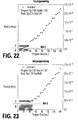
- a first programming round may be implemented setting the reference current for sensing a single bit at the level Ref- 1 as illustrated in Fig. 22.
- a second programming round may be implemented by setting the reference current for sensing a single bit at the level Ref-2 as shown in Fig. 23.
- a third programming round may be implemented by setting the reference current for sensing a single bit at the level Ref-3 as shown in Fig. 24.
- a fourth programming round may be implemented by setting the reference current for sensing a single bit at the level Ref-4 as shown in Fig. 25.
- the number of times which a memory cell may be programmed to be adapted to a particular implementation, and depends on the ability to reliably program amounts of progressive change in resistance and to discriminate between current levels generated when accessing the memory cells.
- the read/program state machine e.g. 277 of Fig. 21
- the read/program state machine is set up to track meet number of programming rounds executed so that the appropriate reference current is supplied to the sensing circuitry.
- Fig. 26 illustrates one basic program algorithm for the programmable resistor eraseless memory cell of an embodiment of the present invention.
- a first reference current value is set for sensing and verifying (block 301).
- a stress/program operation is executed adapted to cause an amount of progressive breakdown such that a program cell will produce an output current when read which is greater than the first reference current value (block 302).
- the stress applied during the program operation can be set so that success is expected after a single stress cycle.
- the stress applied during a program operation can be set so that progressive changes in resistance are caused incrementally using sequences of shorter pulses, which may vary in length and/or voltage level, or may have consistent length and voltage level, allowing more control over final amounts of progressive changes in properties of the memory cell.
- a verify operation is executed to ensure successful programming (block 303). If the verify fails, then the stress program operation is retried with a next stress pulse in a sequence. If the verify passes, then the first program round is done (block 304). As shown in Fig. 26, a second program round 310, a third program round 320, a fourth program round 330, and so on, can be executed using the same basic process, while setting progressively increasing reference currents.
- the programming process includes fixing the n-diffusion electrode at about -2V, and stepping the p-poly electrode from about 0.5V to about 2V, increasing 0.1V per step with constant pulse width (for example 1ms or 10ms), with a verify step between each pulse, and stopping when the cell passes the verify step.
- constant pulse width for example 1ms or 10ms
- the process includes fixing the n-diffusion electrode at about -2V and the p-poly electrode at about 2V to apply constant pulse heights, and applying pulses having constant pulse width (for example 1ms or 10ms), with a verify step between each pulse, and stopping when the cell passes the verify step.
- pulse widths and pulse heights can be varied according to the needs of a particular system.
- the programmable resistor eraseless memory of an embodiment of the present invention demonstrates excellent program disturb and read performance.
- the program disturb performance can be understood with reference to Figs. 27A-27D.
- Fig. 27A a schematic representation of a section of an array is presented, showing word lines 400-403 and bit lines 410-413.
- a memory cell A at the intersection of word line 401 and bit line 411 is to be programmed by applying about 1.8 volts to the electrode on the word line 410 and about negative 1.5 volts to the electrode on the bit line 411.
- a memory cell B at the intersection of word line 401 with an adjacent bit line 412 receives the 1.8 volt word line potential, but the bit line 412 is grounded.
- a memory cell C at the intersection of bit line 411 with an adjacent word line 402 receives the negative 1.5 volt bit line potential, while the word line is grounded.
- Fig. 27B is a representation of selected memory cell A, with the top electrode 420 formed with p-type polysilicon, the bottom electrode 421 formed by an n-type buried diffusion (or well), and the inter-electrode dielectric 422 formed by 15 Angstroms of oxynitride.
- the program potential of about 3.3 volts across the electrodes in a forward bias mode for the p-n junction of the device, applying voltages having absolute values of less than 2 volts, causes a progressively decreasing resistance across the electrodes, resulting in progressively increasing read current, as shown in Fig. 6.
- Fig. 27C shows the condition of unselected memory cell C, with the top electrode 423 formed with p-type polysilicon, the bottom electrode 424 formed by an n-type buried diffusion (or well), and the inter-electrode dielectric 425 formed by 15 Angstroms of oxynitride.
- the bottom electrode receives the negative 1.5 volts bias, while the top electrode is grounded. This is a reverse bias condition for the p-n junction.
- Fig. 27D shows the condition of unselected memory cell B, with the top electrode 426 formed with p-type polysilicon, the bottom electrode 427 formed by an n-type buried diffusion (or well), and the inter-electrode dielectric 428 formed by 15 Angstroms of oxynitride.
- the top electrode of memory cell B receives the 1.8 volt bias, while the bottom electrode is grounded.
- the graph in Fig. 28 shows that program current remains very low after 10000 seconds of program stress on the memory cell biased like memory cell B.
- the graph in Fig. 29 shows that program current remains very low after 10000 seconds of program stress on the memory cell biased like memory cell C. Therefore, program disturb is not observed at the scale of the Figures.
- Fig. 30A a schematic representation of a section of an array is presented, showing word lines 500-503 and bit lines 504-507.
- a memory cell A at the intersection of word line 502 and bit line 505 is to be read by applying a read potential of about 1.3 volts to the electrode on the word line 502 and ground to the electrode on the bit line 505.
- a memory cell B1 at the intersection of word line 502 with an adjacent bit line 506, receives the 1.3 volt word line potential, but the bit line 506 is set at an inhibit potential near 1.3 volts.
- Fig. 30B is a representation of selected memory cell A, with the top electrode 520 formed with p-type polysilicon, the bottom electrode 521 formed by n-type buried diffusion (or well), and the inter-electrode dielectric 522 formed by 15 Angstroms of oxynitride.
- the dielectric has been programmed to a lower resistance state.
- the read potential of about 1.3 volts across the electrodes in a forward bias mode for the p-n junction of the device, causes a current to flow in the device which can be sensed.
- Fig. 30C is a representation of selected memory cell A, with the top electrode 523 formed with p-type polysilicon, the bottom electrode 524 formed by an n-type buried diffusion (or well), and the inter-electrode dielectric 525 formed by 15 Angstroms of oxynitride.
- the dielectric has not been programmed to a lower resistance state.
- the read potential of about 1.3 volts across the electrodes in a forward bias mode for the p-n junction of the device, does not cause a current to flow in the device.
- Fig. 30D shows the condition of unselected memory cell B 1 when it is in a programmed condition, with the top electrode 527 formed with p-type polysilicon, the bottom electrode 528 formed by an n-type buried diffusion (or well), and the inter-electrode dielectric 529 formed by 15 Angstroms of oxynitride.
- the bottom electrode receives the 1.3 volt inhibit bias, while the top electrode is grounded. This is a reverse bias condition for the p-n junction, and essentially no current flows.
- memory cells at locations B2 and C of Fig. 30A will have no current flow, whether they are in the programmed lower resistance state, or the unprogrammed higher resistance state.
- the graph in Fig. 31 shows read current versus gate voltage for a programmed cell on trace 550 and a non-programmed cell ("fresh cell”) on trace 551.
- V g ⁇ 0 when the cell is reverse biased (V g ⁇ 0), essentially no current flows.
- V g above a few tenths of a volt
- small amounts of current flow in both a programmed and unprogrammed cell.
- line 552 in this example, the programmed cell conducts measurably more current than the unprogrammed cell.
- Durability of the memory cell of an embodiment of the present invention is illustrated by the graph in Fig. 32. Read current remains nearly constant for both programmed cells at differing levels of programming, as shown on traces 560 and 561, and for an unprogrammed cell as shown on trace 560 for long read times.
- Fig. 34 shows the read current versus program time graph of Fig. 6, superimposed with a data level threshold and reference current values for storing two bits per cell, while also supporting multiple rounds of programming.
- no program stress is applied to store a data value 00.
- program stress is applied for about 25 seconds.
- program stress is applied for about 35 seconds.
- program stress is applied for about 45 seconds.
- Reference current sources are set for the purposes of sensing the data values.
- a reference current Ref-1.1 is set in this example at about ten microamps.
- a reference current Ref-1.2 is set in this example at about 22 microamps.
- a final reference current Ref-1.3 is set in this example at about 35 microamps.
- Figs. 35 and 36 illustrate application of the programmable resistor eraseless memory of an embodiment of the present invention in "system on a chip” (SOC) embodiments.
- the manufacturing process for the PREM array is fully compatible with standard CMOS manufacturing flows, requiring for example only one additional mask, and therefore is well suited as a compact, non-volatile store in a SOC product.
- CMOS complementary metal-oxide-semiconductor
- n + buried diffusion bottom electrodes only one extra mask is needed, to define the implantation step for the n + buried diffusion while the STI, dielectric film formation and p + -poly gate formation are shared with standard CMOS structure formation.
- the low voltage operation of the PREM makes it a good choice for low voltage and low power environments.
- Fig. 35 illustrates an integrated circuit 600, including a programmable resistance eraseless memory PREM array 601, logic 603, such as application specific logic or programmable gate array logic, and a static random access memory SRAM 602.
- the PREM array 601 can be used to store more permanent data, such as program specifications for a programmable gate array and persistent control parameters.
- the SRAM 602 can be used to store working data used during operation of the logic 603.
- Fig. 36 illustrates another SOC embodiment of the invention.
- the integrated circuit 700 of Fig. 36 includes a programmable resistance eraseless memory PREM array 701, logic 703, such as application specific logic or programmable gate array logic, a static random access memory SRAM 702, and a general purpose processor 704.
- the PREM array 701 can be used to store programs of instructions for execution by the general purpose processor 704.
- instructions stored in the SRAM 702 by an external controller or transferred to the SRAM 702 from the PREM array 701 can be provided for execution by the processor to control the programming of the PREM array.
- the present invention provides a novel non-volatile memory named PREM ( P rogrammable R esistor with E rase-less M emory) where the property of the inter-electrode layer that changes in response to stress is resistance.
- PREM P rogrammable R esistor with E rase-less M emory
- One embodiment of a PREM cell is composed by a p + -polysilicon gate, ultra-thin oxide and n + diffusion, and utilizes the progressive breakdown in ultra-thin oxide as a data storage feature.
- the PREM device can achieve full CMOS-process compatibility, MTP (multi-time programming), MLC (multi-level cell) and low voltage operation (within ⁇ 2V).
- Logic circuits, SRAM and non-volatile PREM can be integrated easily for SOC applications.
- the cell data retention performance is excellent. There is no detected program disturbance phenomenon. There is no detected read disturbance phenomenon.
- Embodiments of the present invention provide a method for programming a memory cell based on applying stress to a memory cell, comprising a first electrode, a second electrode and an inter-electrode layer, to induce a progressive change in a property of the inter-electrode layer.
- the method includes a verify step including generating a signal, such as a cell current, indicating the value of the property in the selected memory cell. Then, the signal is compared with a reference signal to verify programming of the desired data. Because of the progressive nature of the change, many levels of programming can be achieved. The many levels of programming can be applied for programming a single cell more than once, without an erase process, to programming multiple bits in a single cell, and to a combination of multiple bit and multiple time of programming.
Landscapes
- Engineering & Computer Science (AREA)
- Computer Hardware Design (AREA)
- Semiconductor Memories (AREA)
- Read Only Memory (AREA)
Applications Claiming Priority (4)
| Application Number | Priority Date | Filing Date | Title |
|---|---|---|---|
| US62491903A | 2003-07-21 | 2003-07-21 | |
| US624919 | 2003-07-21 | ||
| US10/642,249 US7180123B2 (en) | 2003-07-21 | 2003-08-15 | Method for programming programmable eraseless memory |
| US642249 | 2003-08-15 |
Publications (2)
| Publication Number | Publication Date |
|---|---|
| EP1503384A2 true EP1503384A2 (de) | 2005-02-02 |
| EP1503384A3 EP1503384A3 (de) | 2007-07-18 |
Family
ID=33544782
Family Applications (1)
| Application Number | Title | Priority Date | Filing Date |
|---|---|---|---|
| EP04250188A Withdrawn EP1503384A3 (de) | 2003-07-21 | 2004-01-15 | Verfahren zur Speicherprogrammierung |
Country Status (1)
| Country | Link |
|---|---|
| EP (1) | EP1503384A3 (de) |
Cited By (2)
| Publication number | Priority date | Publication date | Assignee | Title |
|---|---|---|---|---|
| WO2011078917A1 (en) * | 2009-12-21 | 2011-06-30 | Sandisk Corporation | Rewritable memory device with multi-level, write-once memory cells |
| TWI721873B (zh) * | 2019-09-03 | 2021-03-11 | 美商超捷公司 | 在預定程式狀態中使用最終烘烤來改善類比非揮發性記憶體中之讀取電流穩定性的方法 |
Citations (1)
| Publication number | Priority date | Publication date | Assignee | Title |
|---|---|---|---|---|
| US20030003674A1 (en) * | 2001-06-28 | 2003-01-02 | Hsu Sheng Teng | Electrically programmable resistance cross point memory |
Family Cites Families (6)
| Publication number | Priority date | Publication date | Assignee | Title |
|---|---|---|---|---|
| WO1997012368A1 (en) * | 1995-09-29 | 1997-04-03 | Intel Corporation | Multiple writes per a single erase for a nonvolatile memory |
| JP3114630B2 (ja) * | 1996-10-03 | 2000-12-04 | 日本電気株式会社 | 不揮発性半導体メモリおよび書込み読出し方法 |
| US6040993A (en) * | 1998-02-23 | 2000-03-21 | Macronix International Co., Ltd. | Method for programming an analog/multi-level flash EEPROM |
| JP2000348493A (ja) * | 1999-06-03 | 2000-12-15 | Fujitsu Ltd | 不揮発性メモリ回路 |
| US6700151B2 (en) * | 2001-10-17 | 2004-03-02 | Kilopass Technologies, Inc. | Reprogrammable non-volatile memory using a breakdown phenomena in an ultra-thin dielectric |
| FR2846464A1 (fr) * | 2002-10-29 | 2004-04-30 | St Microelectronics Sa | Point memoire, son procede de programmation et son procede de lecture, et circuit integre incorporant de tels points memoire |
-
2004
- 2004-01-15 EP EP04250188A patent/EP1503384A3/de not_active Withdrawn
Patent Citations (1)
| Publication number | Priority date | Publication date | Assignee | Title |
|---|---|---|---|---|
| US20030003674A1 (en) * | 2001-06-28 | 2003-01-02 | Hsu Sheng Teng | Electrically programmable resistance cross point memory |
Cited By (5)
| Publication number | Priority date | Publication date | Assignee | Title |
|---|---|---|---|---|
| WO2011078917A1 (en) * | 2009-12-21 | 2011-06-30 | Sandisk Corporation | Rewritable memory device with multi-level, write-once memory cells |
| US8149607B2 (en) | 2009-12-21 | 2012-04-03 | Sandisk 3D Llc | Rewritable memory device with multi-level, write-once memory cells |
| JP2013515330A (ja) * | 2009-12-21 | 2013-05-02 | サンディスク スリーディー,エルエルシー | マルチレベル・ライトワンス・メモリ・セルを備える書き換え可能メモリデバイス |
| TWI721873B (zh) * | 2019-09-03 | 2021-03-11 | 美商超捷公司 | 在預定程式狀態中使用最終烘烤來改善類比非揮發性記憶體中之讀取電流穩定性的方法 |
| US11017866B2 (en) | 2019-09-03 | 2021-05-25 | Silicon Storage Technology, Inc. | Method of improving read current stability in analog non-volatile memory using final bake in predetermined program state |
Also Published As
| Publication number | Publication date |
|---|---|
| EP1503384A3 (de) | 2007-07-18 |
Similar Documents
| Publication | Publication Date | Title |
|---|---|---|
| US7132350B2 (en) | Method for manufacturing a programmable eraseless memory | |
| US7643346B2 (en) | NAND type nonvolatile semiconductor memory device having sideface electrode shared by memory cells | |
| US5644533A (en) | Flash memory system, and methods of constructing and utilizing same | |
| US6925009B2 (en) | Semiconductor memory | |
| US7133316B2 (en) | Program/erase method for P-channel charge trapping memory device | |
| US7170785B2 (en) | Method and apparatus for operating a string of charge trapping memory cells | |
| US7483307B2 (en) | Method and apparatus for sensing in charge trapping non-volatile memory | |
| US7180123B2 (en) | Method for programming programmable eraseless memory | |
| US20050035429A1 (en) | Programmable eraseless memory | |
| US7474558B2 (en) | Gated diode nonvolatile memory cell array | |
| JP2006512776A (ja) | 直列接続されたトランジスタ列を組込んだプログラマブルメモリアレイ構造およびこの構造を製造して作動させるための方法 | |
| US20060140005A1 (en) | Method and apparatus for operating a non-volatile memory array | |
| KR100354406B1 (ko) | 플래시메모리장치,및이의제조및사용방법 | |
| US7269062B2 (en) | Gated diode nonvolatile memory cell | |
| JP5015420B2 (ja) | プログラマブル消去不要メモリに対するプログラミング方法 | |
| EP1503384A2 (de) | Verfahren zur Speicherprogrammierung | |
| EP1503383A2 (de) | Speicherherstellungsverfahren | |
| EP1501098A2 (de) | Speicher | |
| CN100524763C (zh) | 集成电路、存储单元及其制造方法、存储单元的编程方法 | |
| US7723757B2 (en) | Vertical nonvolatile memory cell, array, and operation |
Legal Events
| Date | Code | Title | Description |
|---|---|---|---|
| PUAI | Public reference made under article 153(3) epc to a published international application that has entered the european phase |
Free format text: ORIGINAL CODE: 0009012 |
|
| AK | Designated contracting states |
Kind code of ref document: A2 Designated state(s): AT BE BG CH CY CZ DE DK EE ES FI FR GB GR HU IE IT LI LU MC NL PT RO SE SI SK TR |
|
| AX | Request for extension of the european patent |
Extension state: AL LT LV MK |
|
| RIC1 | Information provided on ipc code assigned before grant |
Ipc: G11C 11/56 20060101AFI20040402BHEP Ipc: G11C 17/14 20060101ALI20070420BHEP |
|
| PUAL | Search report despatched |
Free format text: ORIGINAL CODE: 0009013 |
|
| AK | Designated contracting states |
Kind code of ref document: A3 Designated state(s): AT BE BG CH CY CZ DE DK EE ES FI FR GB GR HU IE IT LI LU MC NL PT RO SE SI SK TR |
|
| AX | Request for extension of the european patent |
Extension state: AL LT LV MK |
|
| 17P | Request for examination filed |
Effective date: 20080104 |
|
| AKX | Designation fees paid |
Designated state(s): DE FR GB IT |
|
| 17Q | First examination report despatched |
Effective date: 20080502 |
|
| STAA | Information on the status of an ep patent application or granted ep patent |
Free format text: STATUS: EXAMINATION IS IN PROGRESS |
|
| STAA | Information on the status of an ep patent application or granted ep patent |
Free format text: STATUS: THE APPLICATION IS DEEMED TO BE WITHDRAWN |
|
| 18D | Application deemed to be withdrawn |
Effective date: 20170103 |