EP2400318A1 - Strahlungsdetektionsvorrichtung - Google Patents
Strahlungsdetektionsvorrichtung Download PDFInfo
- Publication number
- EP2400318A1 EP2400318A1 EP10743657A EP10743657A EP2400318A1 EP 2400318 A1 EP2400318 A1 EP 2400318A1 EP 10743657 A EP10743657 A EP 10743657A EP 10743657 A EP10743657 A EP 10743657A EP 2400318 A1 EP2400318 A1 EP 2400318A1
- Authority
- EP
- European Patent Office
- Prior art keywords
- pixel
- imaging element
- radiation
- pixels
- detection device
- Prior art date
- Legal status (The legal status is an assumption and is not a legal conclusion. Google has not performed a legal analysis and makes no representation as to the accuracy of the status listed.)
- Withdrawn
Links
Images


Classifications
-
- G—PHYSICS
- G01—MEASURING; TESTING
- G01T—MEASUREMENT OF NUCLEAR OR X-RADIATION
- G01T1/00—Measuring X-radiation, gamma radiation, corpuscular radiation, or cosmic radiation
- G01T1/16—Measuring radiation intensity
- G01T1/20—Measuring radiation intensity with scintillation detectors
- G01T1/2018—Scintillation-photodiode combinations
- G01T1/20181—Stacked detectors, e.g. for measuring energy and positional information
Definitions
- a dual-energy type radiation detection device for example, X-ray detection device
- X-ray detection device is a device to be used for detecting radiation (for example, X-rays) in a low-energy range, and radiation in a high-energy range transmitted through an inspection object (refer to, for example, Patent Documents 1 and 2).
- a radiation detection device With such a radiation detection device, a radiation image in a low-energy range and a radiation image in a high-energy range can be simultaneously obtained.
- an image applied with a predetermined processing for example, a weighted subtraction, superimposition, or the like
- a predetermined processing for example, a weighted subtraction, superimposition, or the like
- various measurements such as measurement of distribution of a plurality of mixed components, detection of a foreign substance that is hardly provided with contrast, or measurement of a weight before cutting, can be realized with high accuracy.
- a dual-energy type radiation detection device for example, a two-stage configuration including a radiation detector that is positioned on the upstream side with respect to a radiation incident direction in which radiation from a radiation source is supplied and detects radiation in a low-energy range, and a radiation detector that is positioned on the downstream side and detects radiation in a high-energy range, can be considered.
- a radiation detector that is positioned on the upstream side with respect to a radiation incident direction in which radiation from a radiation source is supplied and detects radiation in a low-energy range
- a radiation detector that is positioned on the downstream side and detects radiation in a high-energy range
- the present invention has been made in order to solve the above-described problem, and an object thereof is to provide a dual-energy type radiation detection device capable of reducing deviations between images respectively acquired with two-stage radiation detectors.
- a radiation detection device for detecting radiation in a first energy range and radiation in a second energy range higher than the first energy range, made incident in a radiation incident direction, including: (1) a first radiation detector positioned on the upstream side of the radiation incident direction and used for detecting radiation in the first energy range; and (2) a second radiation detector positioned on the downstream side of the radiation incident direction and used for detecting radiation in the second energy range, wherein (3) the first radiation detector includes a first scintillator layer that extends along an image detecting direction and converts an image of the radiation in the first energy range into an optical image, and a first imaging element that includes a plurality of pixels arrayed along the image detecting direction and acquires a first image by the optical image converted in the first scintillator layer, (4) the second radiation detector includes a second scintillator layer that extends along the image detecting direction and converts an image of the radiation in the second energy range into an optical image, and a
- the detection device includes the first radiation detector for radiation in a low-energy range, positioned on the upstream side with respect to the radiation incident direction, and the second radiation detector for radiation in a high-energy range, positioned on the downstream side.
- the pixel width p1 of the imaging element in the first radiation detector and the pixel width p2 of the imaging element in the second radiation detector are set to be different in width from each other (p1 ⁇ p2 or p1 > p2). With such a configuration, it becomes possible to perform high-accuracy measurement of a radiation image with the dual-energy detection device by reducing deviations between images respectively acquired with the imaging element of the first radiation detector and the imaging element of the second radiation detector.
- the pixel widths p1 and p2 of the above-described imaging elements are preferably set by considering the distance ⁇ d between the first imaging element and the second imaging element.
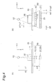
- Fig. 1 is a figure including views showing a configuration of an embodiment of an X-ray detection device, which is a radiation detection device, and (a) in Fig. 1 shows a sectional side view, and (b) in Fig. 1 shows a sectional front view.
- X-rays are assumed as radiation to be detected by the detection device, and a configuration of an X-ray detection device, which is a kind of radiation detection device, will be described.
- Such an X-ray detection device can be preferably applied to a non-destructive inspection or the like of an inspection object described above,
- This X-ray detection device 1A has a two-stage configuration including a first X-ray detector (first radiation detector) 10 that is positioned on the upstream side of the X-ray incident direction and is used for detecting X-rays in the low-energy range, and a second X-ray detector (second radiation detector) 20 that is positioned on the downstream side and is used for detecting X-rays in the high-energy range.
- first radiation detector first radiation detector
- second radiation detector 20 that is positioned on the downstream side and is used for detecting X-rays in the high-energy range.
- the first X-ray detector 10 includes a first support substrate 15 and a first imaging element 12 and a first scintillator layer 11 placed on the support substrate 15, and is disposed so that the first scintillator layer 11 is on the upstream side with respect to the X-ray incident direction.
- the first scintillator layer 11 is made of a predetermined scintillator material, extends along an X-ray image detecting direction (horizontal direction in (b) in Fig. 1 ) perpendicular to the X-ray incident direction so that its longitudinal direction is along the image detecting direction, and converts an image of X-rays in the low-energy range out of X-rays made incident on the detection device 1A into an optical image.
- the first imaging element 12 is optically connected to the surface on the downstream side of the scintillator layer 11, the first imaging element 12 is optically connected.
- the imaging element 12 includes a plurality of pixels 13 one-dimensionally arrayed along the image detecting direction, and by acquiring a first image caused by the optical image converted in the scintillator layer 11, acquires a first X-ray image in the low-energy range.
- the image detecting direction in the first X-ray detector 10 matches the longitudinal direction of the pixel array of the first imaging element 12 in the present embodiment.
- the second X-ray detector 20 includes a second support substrate 25 and a second imaging element 22 and a second scintillator layer 21 placed on the support substrate 25, and is disposed so that the second scintillator layer 21 is on the upstream side with respect to the X-ray incident direction.
- the second scintillator layer 21 is made of a predetermined scintillator material, extends along the X-ray image detecting direction so that its longitudinal direction is along the image detecting direction, and converts an image of X-rays in the high-energy range out of the X-rays made incident on the detection device 1A into an optical image.
- the filter 18 is a filter for selecting energy components of X-rays that pass through from the first X-ray detector 10 to the second X-ray detector 20, and is disposed or changed as appropriate when selecting or changing an energy range of X-rays desired to be detected by the second X-ray detector 20.
- a first pixel width p1 in the image detecting direction of each of the plurality of pixels 13 in the first imaging element 12 positioned on the upstream side and a second pixel width p2 of each of the plurality of pixels 23 in the second imaging element 22 positioned on the downstream side are set to be different in width from each other (p1 ⁇ p2 or p1 > p2) by considering the distance ⁇ d between the first and second imaging elements 12 and 22 (refer to (b) in Fig. 1 ).
- FIG. 2 is a figure including schematic views showing an example of configurations of an X-ray detection device and an X-ray detection system including the detection device, and (a) in Fig. 2 shows a side view, and (b) in Fig. 2 shows a front view.
- Fig. 2 concerning the configuration of the X-ray detection device 50, only the structures of the pixels 13 and 23 in the imaging elements 12 and 22 in each of the first and second X-ray detectors are shown. Configurations of other parts of the X-ray detection device 50 are the same as, for example, those in the X-ray detection device 1A shown in Fig. 1 .
- the X-ray detection system of this configuration example is configured as an inspection system for performing a non-destructive inspection of an inspection object 56 that is conveyed by a belt conveyor 55.
- an X-ray source 52 as a radiation source that supplies X-rays (radiation) for inspection to the inspection object 56 is disposed.
- a dual-energy X-ray detection device 50 that detects an X-ray image in a low-energy range and an X-ray image in a high-energy range of X-rays that passed through the inspection object 56 is disposed.
- a conveying direction of the inspection object 56 by the belt conveyor 55 is defined as a y-axis direction (horizontal direction in (a) in Fig. 2 ), an X-ray incident direction from the X-ray source 52 to the detection device 50, perpendicular to the y-axis direction, is defined as a z-axis direction (vertical direction in (a) and (b) in Fig.
- an image detecting direction (array direction of the pixels 13, 23) in the imaging elements 12 and 22 of the detection device 50, perpendicular to the y-axis direction and the z-axis direction, is defined as an x-axis direction (horizontal direction in (b) in Fig. 2 ).
- the image detecting direction in the X-ray detector is a direction perpendicular to the conveying direction of the inspection object.
- the plurality of pixels 13 in the first imaging element 12 are divided into a plurality of pixel units each consisting of one pixel as a unit, and one pixel simply corresponds to one pixel unit.
- the plurality of pixels 23 in the second imaging element 22 are divided into a plurality of pixel units each consisting of one pixel as a unit, and similar to the first imaging element 12, one pixel simply corresponds to one pixel unit.
- the detection device includes the first X-ray detector 10 for X-rays in the low-energy range, positioned on the upstream side with respect to the X-ray incident direction, and the second X-ray detector 20 for X-rays in the high-energy range, positioned on the downstream side.
- the pixel width p1 of the pixel 13 of the imaging element 12 in the first X-ray detector 10 and the pixel width p2 of the pixel 23 of the imaging element 22 in the second X-ray detector 20 are set to be different in width from each other.
- the pixel widths p1 and p2 in the imaging elements 12 and 22 are set by considering the distance ⁇ d between the first imaging element 12 and the second imaging element 22.
- Patent Document 1 it is described that correction is applied so that sizes of a plurality of radiation image data become equal to each other.
- image processing takes time because image data correction is performed by software, and it is difficult to apply this to the field in which high-speed image processing is required as in the case of, for example, a non-destructive inspection of an inspection object.
- the X-ray detection device reduces deviations between images by hardware by means of the pixel structures of the imaging elements, and accordingly realizes high-speed measurement of X-ray images.
- the plurality of pixels 13 in the first imaging element 12 are divided into a plurality of pixel units each consisting of one pixel as a unit
- the plurality of pixels 23 in the second imaging element 22 are also divided into a plurality of pixel units each consisting of one pixel as a unit.
- Pixel widths and pixel unit widths in the first and second imaging elements 12 and 22 are set to be constant entirely in the image detecting direction in the configurations of Fig. 1 and Fig. 2 . These pixel widths may be set so that the pixel unit width w2 (pixel width p2) in the second imaging element 22 increases (the pixel width increases) from the central portion toward the peripheral portion in the image detecting direction in which the plurality of pixel units are arrayed. With such a configuration, influences, etc., of the X-ray incident angle that increases from the central portion toward the peripheral portion can be reduced.
- the pixel widths in the direction (y-axis direction) perpendicular to the image detecting direction in the first and second imaging elements 12 and 22 may be set to be equal to both of the imaging elements 12 and 22 as shown in (a) in Fig. 2 . Alternatively, it may also be configured such that the pixel width in the y-axis direction in the second imaging element 22 is set to be larger than the pixel width in the first imaging element 12.
- the entire configuration of the X-ray detection device is not limited to the configuration shown in Fig. 1 , and specifically, various configurations can be used.
- An example of such configurations of the X-ray detection device is shown in Fig. 3 .
- Fig. 3 is a figure including views showing a configuration of another embodiment of an X-ray detection device, which is a radiation detection device, and (a) in Fig. 3 shows a sectional side view, and (b) in Fig. 3 shows a sectional front view.
- the X-ray detection device 1B includes a first X-ray detector 10 that is positioned on the upstream side of the X-ray incident direction and is used for detecting X-rays in the low-energy range, and a second X-ray detector 20 that is positioned on the downstream side and is used for detecting X-rays in the high-energy range.
- the configuration of the second X-ray detector 20 out of these detectors is the same as the configuration shown in Fig. 1 .
- the first X-ray detector 10 includes a first support substrate 15 and a first imaging element 12 and a first scintillator layer 11 placed on the support substrate 15, and opposite to the configuration shown in Fig. 1 , the first support substrate 15 is on the upstream side with respect to the X-ray incident direction. Further, in the present embodiment, between the first scintillator layer 11 of the first X-ray detector 10 and the second scintillator layer 21 of the second X-ray detector 20, a filter or the like is not installed.
- the first pixel width p1 in the image detecting direction of the pixels 13 in the first imaging element 12 and the second pixel width p2 of the pixels 23 in the second imaging element 22 are set to be different in width from each other by considering the distance ⁇ d between the first and second imaging elements 12 and 22.
- various configurations can be used as the entire configuration of the X-ray detection device.
- FIG. 4 is a figure including schematic views showing another example of configurations of an X-ray detection device and an X-ray detection system including the detection device, and (a) in Fig. 4 shows a side view, and (b) in Fig. 4 shows a front view.
- the configuration except for the structure of the pixels 23 in the imaging element 22 in the second X-ray detector is the same as the configuration shown in Fig. 2 .
- the plurality of pixels 13 in the first imaging element 12 are divided into a plurality of pixel units each consisting of one pixel as a unit, and one pixel simply corresponds to one pixel unit.
- the plurality of pixels 23 in the second imaging element 22 are divided into a plurality of pixel units each consisting of a plurality (specifically, two in Fig. 4 ) of pixels as a unit, and two pixels correspond to one pixel unit.
- each pixel unit (one pixel 13) in the imaging element 12 and each pixel unit (two pixels 23) in the imaging element 22 correspond to each other.
- the pixel structure of the second imaging element 22 in the X-ray detector on the downstream side it may also be configured such that the plurality of pixels 23 are divided into a plurality of pixel units each consisting of a plurality of pixels as a unit, and each pixel unit corresponds to the pixel of the first imaging element 12, and the second pixel width p2 is set to be smaller than the first pixel width p1.
- the pixel structure of the first imaging element 12 on the upstream side may also be similarly configured so that the plurality of pixels 13 are divided into a plurality of pixel units each consisting of a plurality of pixels as a unit.
- the plurality of pixels 13 in the first imaging element 12 are divided into a plurality of pixel units each consisting of one or a plurality of pixels as a unit
- the plurality of pixels 23 in the second imaging element 22 are divided into a plurality of pixel units each consisting of one or a plurality of pixels as a unit
- the second pixel unit width w2 of each of the plurality of pixel units in the second imaging element 22 is set to be larger than the first pixel unit width w1 of each of the plurality of pixel units in the first imaging element 12.
- the pixel structure in the imaging elements 12 and 22 in the above-described configuration example, the pixel structure is segmented into a plurality of pixels 13, 23 arrayed one-dimensionally. On the other hand, in the direction (y-axis direction) perpendicular to the image detecting direction, the pixel structure consists of a single pixel.
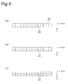
- Fig. 5 includes views showing examples of pixel structures in the second imaging element, and (a) in Fig. 5 is a front view showing a pixel structure in the second imaging element 22, (b) in Fig. 5 is a top view (viewed from the X-ray source side) showing a first example of the pixel structure in the second imaging element, and (c) in Fig. 5 is a top view showing a second example of the pixel structure.
- the pixel structure viewed from the front is the same as shown in (a) in Fig. 5 .
- pixels are not segmented in the y-axis direction perpendicular to the image detecting direction, and the plurality of pixels 23 are one-dimensionally arrayed in one row in the pixel structure (strip type).
- pixels are segmented into two in the y-axis direction, and the plurality of pixels 23 are one-dimensionally arrayed in two rows in the pixel structure (lattice type).
- pixel structures of the first and second imaging elements 12 and 22 to be used in X-ray detectors generally, a configuration of a one-dimensional imaging element including a plurality of pixels one-dimensionally arrayed in one row along the image detecting direction, or a configuration of a two-dimensional imaging element including a plurality of pixels segmented into two or more also in the direction perpendicular to the image detecting direction and arrayed in a plurality of rows along the image detecting direction can be used. Further, in such a configuration, the image detecting directions in the first and second X-ray detectors respectively match the pixel array directions of the first and second imaging elements 12 and 22.
- the longitudinal direction of the pixel array serves as the image detecting direction.
- the longitudinal direction serves as the image detecting direction.
- the second imaging element 22 when the plurality of pixels 23 thereof are used divided into a plurality of pixel units each consisting of a plurality of pixels as a unit, such pixel units can be realized, for example, by binning processing including performing summing, etc., of detection signals on a pixel-unit basis, for the detection signals acquired by the pixels 23.
- a pixel unit control section for controlling binning processing according to the number of pixels in the set pixel unit is preferably provided. Accordingly, it becomes possible for the pixel unit in the imaging element 22 to be preferably set or changed as appropriate.
- Fig. 6 is a diagram showing a variation example of the X-ray detection device shown in Fig. 4 .
- the plurality of pixels 13 in the imaging element 12 are divided into a plurality of pixel units each consisting of one pixel as a unit.
- the plurality of pixels 23 in the imaging element 22 are divided into a plurality of pixel units each consisting of a plurality of pixels as a unit.
- a pixel unit control section 30 is provided for the imaging element 22.
- binning processing in the imaging element 22 can be preferably performed according to the number of pixels in the set pixel unit.
- a distance information input section 31 and a pixel unit setting section 32 are provided for the pixel unit control section 30, a distance information input section 31 and a pixel unit setting section 32 are provided.
- the distance information input section 31 is used for inputting distance information from the X-ray source 52 to the X-ray detectors in the X-ray detection system (refer to Fig. 4 ).
- Distance information in this case is, for example, the distance d1 from the position of the X-ray source 52 to the first imaging element 12 or the distance d2 from the position of the X-ray source 52 to the second imaging element 22.
- the pixel unit setting section 32 performs settings of the number of pixels which a pixel unit should consist of in the second imaging element 22 or pixel arrangement of those pixels, based on distance information input from the input section 31.
- the pixel unit control section 30 controls binning processing in the imaging element 22 based on information on the pixel unit set in this setting section 32.
- image signals output from the imaging elements 12 and 22 of the X-ray detection device are input to an image acquisition section 33. Then, in this image acquisition section 33, data of a first image imaged with the imaging element 12 corresponding to an X-ray image in the low-energy range and data of a second image imaged with the imaging element 22 corresponding to an X-ray image in the high-energy range are acquired.
- predetermined arithmetic processing for example, a weighted subtraction, superimposition operation, or the like is applied in an image processing section 34.
- An image finally obtained through this arithmetic processing (for example, an inspection image in a non-destructive inspection system) is displayed on an image display section 35 to an operator as appropriate.
- image acquisition section 33, image processing section 34, and image display section 35, etc. can also be applied to the configuration shown in Fig. 2 in the same manner.
- the first imaging element 12 of the first X-ray detector when the plurality of pixels 13 thereof are divided into a plurality of pixel units each consisting of a plurality of pixels as a unit, similar to the above-described pixel unit control section 30 for the second imaging element 22, a pixel unit control section may be provided for the plurality of pixels 13 of the first imaging element 12.
- the X-ray detection device according to the above-described embodiments will be further described along with an example of a specific pixel array structure thereof.
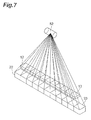
- Fig. 7 is a view showing an example of specific pixel structures of the imaging elements 12 and 22 in the X-ray detection device.
- Fig. 8 is a view showing a correspondence relationship between pixel units in the imaging elements 12 and 22 shown in Fig. 7 . This example corresponds to a specific example of the configuration shown in Fig. 2 .
- one pixel 13 simply corresponds to one pixel unit.
- one pixel 23 simply corresponds to one pixel unit.
- the first pixel width p1 in the first imaging element 12 is set to 0.8 mm
- the second pixel width p2 in the second imaging element 22 is set to 0.9 mm.
- the imaging elements 12 and 22 by configuring the imaging elements 12 and 22 so that the pixel unit widths satisfy w1 ⁇ w2 (pixel widths satisfy p1 ⁇ p2), it becomes possible to prevent pixel deviations between the first and second images respectively acquired with the imaging element 12 of the first X-ray detector and the imaging element 22 of the second X-ray detector.
- the correspondence relationship between the pixel units of the imaging elements 12 and 22 is fixed, therefore, the distance between the X-ray source and the X-ray detection device must also be substantially fixed.
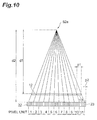
- Fig. 9 is a view showing another example of the specific pixel structures of the imaging elements 12 and 22 in the X-ray detection device.
- Fig. 10 and Fig. 11 respectively show correspondence relationships between pixel units of the imaging elements 12 and 22 shown in Fig. 9 .
- the present example corresponds to a specific example of the configuration shown in Fig. 4 .
- one pixel 13 simply corresponds to one pixel unit.
- four pixels 23 correspond to one pixel unit.
- the first pixel width p1 in the first imaging element 12 is set to 0.8 mm
- the second pixel width p2 in the second imaging element 22 is set to 0.225 mm.
- Fig. 10 and Fig. 11 show an example of such a method for changing the setting of the pixel units.
- the number of pixels constituting each of the pixel units 1 to 11 in the second imaging element 22 is fixed to 4.
- Concerning positions of the pixels constituting the pixel unit, in the pixel units 4 to 8 in a central portion with small pixel deviations, the constituent pixels are the same for both the positions 52a and 52b or the X-ray source.
- the constituent pixels are set shifted by one between the positions 52a and 52b of the X-ray source.
- Fig. 12 includes views showing pixel structures in the first and second imaging elements to be used in the X-ray detection device.
- Fig. 12 includes views showing pixel structures in the first and second imaging elements to be used in the X-ray detection device.
- FIG. 12 In each of the three configuration examples (a) to (c) shown in Fig. 12 , only one pixel unit in the first imaging element 12 on the upstream side and a corresponding one pixel unit in the second imaging element 22 on the downstream side are shown.
- the example of the pixel structure shown in (c) in Fig. 12 indicates an example of a configuration in which a pixel unit in the first imaging element also consists of a plurality of pixels.
- pixels are segmented in the direction perpendicular to the image detecting direction as well.
- each of the first imaging element and the second imaging element is preferably a one-dimensional imaging element including a plurality of pixels one-dimensionally arrayed in a row along the image detecting direction, or a two-dimensional imaging element including a plurality of pixels arrayed in a plurality of rows along the image detecting direction.
- the radiation detection device is not limited to the above-described embodiments and configuration examples, but can be modified in many ways.
- the above-described embodiments describe an X-ray detection device configured by assuming X-rays as radiation to be detected, however, the above-described configurations can also be applicable to a radiation detection device for detecting radiation other than X-rays.
- configurations of the first and second radiation detectors various configurations such as, for example, a configuration in which the support substrate is omitted from the configuration of Fig. 1 , can be specifically used.
- each of the first and second radiation detectors includes a scintillator layer that extends along the image detecting direction and converts a radiation image into an optical image and an imaging element that includes a plurality of pixels arrayed in one or a plurality of rows along the image detecting direction and acquires an image by the optical image converted in the scintillator layer.
- the radiation detection device is a radiation detection device that detects radiation in a first energy range and radiation in a second energy range higher than the first energy range, made incident in a radiation incident direction, and includes (1) a first radiation detector that is positioned on the upstream side with respect to the radiation incident direction and is used for detecting radiation in the first energy range; and (2) a second radiation detector that is positioned on the downstream side with respect to the radiation incident direction and is used for detecting radiation in the second energy range, wherein (3) the first radiation detector includes a first scintillator layer that extends along an image detecting direction and converts an image of the radiation in the first energy range into an optical image, and a first imaging element that includes a plurality of pixels arrayed along the image detecting direction and acquires a first image corresponding to the optical image converted by the first scintillator layer, (4) the second radiation detector includes a second scintillator layer that extends along the image detecting direction and converts an image of the radiation in the second energy range
- the second pixel unit width w2 (or the second pixel width p2) in the second imaging element may be set so as to increase (the pixel width increase) from the central portion toward the peripheral portion in the image detecting direction in which a plurality of pixel units are arrayed. With such a configuration, influences of the radiation incident angle that increases from the central portion toward the peripheral portion can be reduced.
- first and second imaging elements As a specific configuration of the first and second imaging elements, a configuration in which the plurality of pixels in the first imaging element are divided into the plurality of pixel units each consisting of one pixel as a unit, and the plurality of pixels in the second imaging element are divided into the plurality of pixel units each consisting of one pixel as a unit, and the second pixel width p2 is set to be larger than the first pixel width p1 (p1 ⁇ p2) can be used.
- a configuration in which the plurality of pixels in the first imaging element are divided into the plurality of pixel units each consisting of one pixel as a unit, the plurality of pixels in the second imaging element are divided into the plurality of pixel units each consisting of a plurality of pixels as a unit, and the second pixel width p2 is set to be smaller than the first pixel width p1 (p1 > p2) can be used.
- a pixel unit control section is preferably provided for controlling binning processing according to the number of pixels in the set pixel unit for the plurality of pixels in the second imaging element. Accordingly, it becomes possible for the pixel unit in the second imaging element to be preferably set or changed as appropriate.
- Each of the first imaging element and the second imaging element is preferably a one-dimensional imaging element including a plurality of pixels one-dimensionally arrayed in a row along the image detecting direction, or a two-dimensional imaging element including a plurality of pixels arrayed in a plurality of rows along the image detecting direction.
- the image detecting directions in the first and second radiation detectors match the pixel array directions of the first and second imaging elements, respectively.
- the present invention can be used as a dual-energy type radiation detection device capable of reducing deviations between images respectively acquired with two-stage radiation detectors.
- 1A, 1B - X-ray detection device (radiation detection device), 10 - first X-ray detector (first radiation detector), 11 - first scintillator layer, 12 - first imaging element, 13 - pixel, 15 - first support substrate, 20 - second X-ray detector (second radiation detector), 21 - second scintillator layer, 22 - second imaging element 23 - pixel, 25 - second support substrate, 18 - filter, 30 - pixel unit control section, 31 - distance information input section, 32 - pixel unit setting section, 33 - image acquisition section, 34 - image processing section, 35 - image display section, 50 - X-ray detection device, 52 - X-ray source, 55 - belt conveyor, 56 - inspection object.
Landscapes
- Physics & Mathematics (AREA)
- Health & Medical Sciences (AREA)
- Life Sciences & Earth Sciences (AREA)
- General Physics & Mathematics (AREA)
- High Energy & Nuclear Physics (AREA)
- Molecular Biology (AREA)
- Spectroscopy & Molecular Physics (AREA)
- Measurement Of Radiation (AREA)
- Analysing Materials By The Use Of Radiation (AREA)
Applications Claiming Priority (2)
| Application Number | Priority Date | Filing Date | Title |
|---|---|---|---|
| JP2009037680A JP2010190830A (ja) | 2009-02-20 | 2009-02-20 | 放射線検出装置 |
| PCT/JP2010/051801 WO2010095530A1 (ja) | 2009-02-20 | 2010-02-08 | 放射線検出装置 |
Publications (2)
| Publication Number | Publication Date |
|---|---|
| EP2400318A1 true EP2400318A1 (de) | 2011-12-28 |
| EP2400318A4 EP2400318A4 (de) | 2016-11-02 |
Family
ID=42633813
Family Applications (1)
| Application Number | Title | Priority Date | Filing Date |
|---|---|---|---|
| EP10743657.8A Withdrawn EP2400318A4 (de) | 2009-02-20 | 2010-02-08 | Strahlungsdetektionsvorrichtung |
Country Status (4)
| Country | Link |
|---|---|
| US (1) | US20120025086A1 (de) |
| EP (1) | EP2400318A4 (de) |
| JP (1) | JP2010190830A (de) |
| WO (1) | WO2010095530A1 (de) |
Cited By (5)
| Publication number | Priority date | Publication date | Assignee | Title |
|---|---|---|---|---|
| EP2479557A1 (de) * | 2009-09-18 | 2012-07-25 | Hamamatsu Photonics K.K. | Strahlungsdetektor |
| US9329301B2 (en) | 2009-09-18 | 2016-05-03 | Hamamatsu Photonics K. K. | Radiation detecting device |
| EP2427112A4 (de) * | 2009-05-08 | 2016-07-13 | L 3 Comm Security & Detection | Dual-energy-bildgebungssystem |
| GB2545947A (en) * | 2015-12-29 | 2017-07-05 | Nuctech Co Ltd | Dual-energy detection apparatus, system and method |
| WO2018020258A1 (en) * | 2016-07-28 | 2018-02-01 | Smiths Heimann Sas | Inspection system with a matrix and method |
Families Citing this family (9)
| Publication number | Priority date | Publication date | Assignee | Title |
|---|---|---|---|---|
| JP5452131B2 (ja) * | 2009-08-24 | 2014-03-26 | アンリツ産機システム株式会社 | X線検出器およびx線検査装置 |
| JP5295915B2 (ja) | 2009-09-18 | 2013-09-18 | 浜松ホトニクス株式会社 | 放射線検出装置 |
| JP5616182B2 (ja) * | 2010-09-28 | 2014-10-29 | 株式会社イシダ | X線検査装置 |
| US8440978B2 (en) * | 2010-10-22 | 2013-05-14 | Varian Medical Systems International Ag | Method and apparatus for multi-layered high efficiency mega-voltage imager |
| JP5852415B2 (ja) | 2011-11-08 | 2016-02-03 | 浜松ホトニクス株式会社 | 非破壊検査装置及び当該装置での輝度データの補正方法 |
| DE102013219821A1 (de) * | 2013-09-30 | 2015-04-02 | Fraunhofer-Gesellschaft zur Förderung der angewandten Forschung e.V. | Röntgendetektor |
| CN105242322A (zh) | 2014-06-25 | 2016-01-13 | 清华大学 | 探测器装置、双能ct系统和使用该系统的检测方法 |
| US11071514B2 (en) | 2018-11-16 | 2021-07-27 | Varex Imaging Corporation | Imaging system with energy sensing and method for operation |
| JP7250331B2 (ja) * | 2019-07-05 | 2023-04-03 | 株式会社イシダ | 画像生成装置、検査装置及び学習装置 |
Family Cites Families (18)
| Publication number | Priority date | Publication date | Assignee | Title |
|---|---|---|---|---|
| US4626688A (en) * | 1982-11-26 | 1986-12-02 | Barnes Gary T | Split energy level radiation detection |
| US4963746A (en) * | 1986-11-25 | 1990-10-16 | Picker International, Inc. | Split energy level radiation detection |
| JP2627086B2 (ja) * | 1989-10-18 | 1997-07-02 | 富士写真フイルム株式会社 | 放射線画像読取装置 |
| US6031892A (en) * | 1989-12-05 | 2000-02-29 | University Of Massachusetts Medical Center | System for quantitative radiographic imaging |
| JPH042907A (ja) | 1990-04-20 | 1992-01-07 | Hitachi Medical Corp | X線非破壊検査装置 |
| JPH08160145A (ja) * | 1994-12-06 | 1996-06-21 | Toshiba Corp | X線検出器 |
| US6052433A (en) * | 1995-12-29 | 2000-04-18 | Advanced Optical Technologies, Inc. | Apparatus and method for dual-energy x-ray imaging |
| JP3461236B2 (ja) * | 1996-01-19 | 2003-10-27 | キヤノン株式会社 | 放射線撮影装置並びに画像処理方法及び装置 |
| JP2000298198A (ja) | 1999-02-08 | 2000-10-24 | Fuji Photo Film Co Ltd | 放射線画像データ取得方法および装置 |
| US6243441B1 (en) * | 1999-07-13 | 2001-06-05 | Edge Medical Devices | Active matrix detector for X-ray imaging |
| US6437338B1 (en) * | 1999-09-29 | 2002-08-20 | General Electric Company | Method and apparatus for scanning a detector array in an x-ray imaging system |
| JP3987676B2 (ja) * | 2000-07-10 | 2007-10-10 | 株式会社日立メディコ | X線計測装置 |
| US6922457B2 (en) * | 2001-11-29 | 2005-07-26 | Kabushiki Kaisha Toshiba | Computer tomography apparatus |
| EP1537407A1 (de) * | 2002-09-04 | 2005-06-08 | Koninklijke Philips Electronics N.V. | Streustrahlenraster für ct scanner |
| DE102004006547A1 (de) * | 2004-01-16 | 2005-08-11 | Siemens Ag | Röntgendetektormodul für spektral aufgelöste Messungen |
| US7505554B2 (en) * | 2005-07-25 | 2009-03-17 | Digimd Corporation | Apparatus and methods of an X-ray and tomosynthesis and dual spectra machine |
| US7405406B1 (en) * | 2006-04-21 | 2008-07-29 | Radiation Monitoring Devices, Inc. | Two-sided scintillation detectors and related methods |
| US7638776B2 (en) * | 2006-08-21 | 2009-12-29 | Endicott Interconnect Technologies, Inc. | Staggered array imaging system using pixilated radiation detectors |
-
2009
- 2009-02-20 JP JP2009037680A patent/JP2010190830A/ja active Pending
-
2010
- 2010-02-08 US US13/201,022 patent/US20120025086A1/en not_active Abandoned
- 2010-02-08 EP EP10743657.8A patent/EP2400318A4/de not_active Withdrawn
- 2010-02-08 WO PCT/JP2010/051801 patent/WO2010095530A1/ja active Application Filing
Non-Patent Citations (1)
| Title |
|---|
| See references of WO2010095530A1 * |
Cited By (12)
| Publication number | Priority date | Publication date | Assignee | Title |
|---|---|---|---|---|
| EP2427112A4 (de) * | 2009-05-08 | 2016-07-13 | L 3 Comm Security & Detection | Dual-energy-bildgebungssystem |
| EP2479557A1 (de) * | 2009-09-18 | 2012-07-25 | Hamamatsu Photonics K.K. | Strahlungsdetektor |
| EP2479557A4 (de) * | 2009-09-18 | 2014-12-03 | Hamamatsu Photonics Kk | Strahlungsdetektor |
| US8981310B2 (en) | 2009-09-18 | 2015-03-17 | Hamamatsu Photonics K.K. | Radiation detecting device |
| US9329301B2 (en) | 2009-09-18 | 2016-05-03 | Hamamatsu Photonics K. K. | Radiation detecting device |
| EP2479557B1 (de) | 2009-09-18 | 2017-07-26 | Hamamatsu Photonics K.K. | Strahlungsdetektor |
| GB2545947A (en) * | 2015-12-29 | 2017-07-05 | Nuctech Co Ltd | Dual-energy detection apparatus, system and method |
| US10401308B2 (en) | 2015-12-29 | 2019-09-03 | Nuctech Company Limited | Dual-energy detection apparatus, system and method |
| GB2545947B (en) * | 2015-12-29 | 2020-07-08 | Nuctech Co Ltd | Dual-energy detection apparatus, system and method |
| WO2018020258A1 (en) * | 2016-07-28 | 2018-02-01 | Smiths Heimann Sas | Inspection system with a matrix and method |
| CN110140066A (zh) * | 2016-07-28 | 2019-08-16 | 德国史密斯海曼简化股份公司 | 具有矩阵的检查系统和方法 |
| US10948623B2 (en) | 2016-07-28 | 2021-03-16 | Smiths Heimann Sas | Inspection system with a matrix and method |
Also Published As
| Publication number | Publication date |
|---|---|
| EP2400318A4 (de) | 2016-11-02 |
| JP2010190830A (ja) | 2010-09-02 |
| WO2010095530A1 (ja) | 2010-08-26 |
| US20120025086A1 (en) | 2012-02-02 |
Similar Documents
| Publication | Publication Date | Title |
|---|---|---|
| EP2400318A1 (de) | Strahlungsdetektionsvorrichtung | |
| DK2479558T3 (en) | radiation detecting | |
| US8981310B2 (en) | Radiation detecting device | |
| KR101950515B1 (ko) | 투과 x선 분석 장치 및 방법 | |
| EP2479559B1 (de) | Strahlungsdetektor | |
| EP2960686A1 (de) | Detektorvorrichtung, ct-system mit dualer energie und erkennungsverfahren mit dem system | |
| EP2734835B1 (de) | Phasenabbildung | |
| US20110096903A1 (en) | Multiview x-ray inspection system | |
| EP2251680B2 (de) | Röntgenstrahlinspektionsvorrichtung | |
| US20230344958A1 (en) | Imaging unit and radiation image acquisition system | |
| Olivo et al. | A non-free-space propagation x-ray phase contrast imaging method sensitive to phase effects in two directions simultaneously | |
| JP2009236633A (ja) | X線異物検査装置 | |
| CN109891589B (zh) | 检测器 | |
| US20200241150A1 (en) | Electromagnetic wave detection module, electromagnetic wave detection module array, and non-destructive inspection apparatus | |
| JP3435648B2 (ja) | X線検査装置 | |
| EP3220134B1 (de) | Röntgenstrahlinspektionsvorrichtung | |
| EP3951436A1 (de) | Detektoranordnung und vorrichtung zur absorptionsabbildung mit dieser detektoranordnung | |
| RU2403593C1 (ru) | Матричный рентгеновский приемник для сканирующего рентгеновского аппарата | |
| JPH03189585A (ja) | X線センサアレイ及びx線受像装置 | |
| CN219016144U (zh) | 一种基于tdi技术的x射线安检机 | |
| EP4206745A1 (de) | Bildgebungseinheit und bildgebungssystem | |
| JP6506629B2 (ja) | X線受光装置およびこれを備えたx線検査装置 | |
| JP2013210390A (ja) | 放射線検出装置 | |
| EP4365638A1 (de) | Strahlungsdetektor | |
| KR101688810B1 (ko) | 선형 디텍터를 이용한 면상 엑스선 촬영장치 |
Legal Events
| Date | Code | Title | Description |
|---|---|---|---|
| PUAI | Public reference made under article 153(3) epc to a published international application that has entered the european phase |
Free format text: ORIGINAL CODE: 0009012 |
|
| 17P | Request for examination filed |
Effective date: 20110823 |
|
| AK | Designated contracting states |
Kind code of ref document: A1 Designated state(s): AT BE BG CH CY CZ DE DK EE ES FI FR GB GR HR HU IE IS IT LI LT LU LV MC MK MT NL NO PL PT RO SE SI SK SM TR |
|
| DAX | Request for extension of the european patent (deleted) | ||
| STAA | Information on the status of an ep patent application or granted ep patent |
Free format text: STATUS: THE APPLICATION HAS BEEN WITHDRAWN |
|
| RA4 | Supplementary search report drawn up and despatched (corrected) |
Effective date: 20160930 |
|
| RIC1 | Information provided on ipc code assigned before grant |
Ipc: G01T 1/20 20060101AFI20160926BHEP Ipc: G01N 23/04 20060101ALI20160926BHEP Ipc: G01T 7/00 20060101ALI20160926BHEP |
|
| 18W | Application withdrawn |
Effective date: 20161005 |