EP2399282B1 - Integrierte schaltkreise enthaltend isolationsmaterial und dessen verwendung in integrierten schaltkreisen - Google Patents
Integrierte schaltkreise enthaltend isolationsmaterial und dessen verwendung in integrierten schaltkreisen Download PDFInfo
- Publication number
- EP2399282B1 EP2399282B1 EP10704527.0A EP10704527A EP2399282B1 EP 2399282 B1 EP2399282 B1 EP 2399282B1 EP 10704527 A EP10704527 A EP 10704527A EP 2399282 B1 EP2399282 B1 EP 2399282B1
- Authority
- EP
- European Patent Office
- Prior art keywords
- irmof
- integrated circuits
- insulation material
- irmofs
- dielectric constants
- Prior art date
- Legal status (The legal status is an assumption and is not a legal conclusion. Google has not performed a legal analysis and makes no representation as to the accuracy of the status listed.)
- Not-in-force
Links
Images
Classifications
-
- H—ELECTRICITY
- H10—SEMICONDUCTOR DEVICES; ELECTRIC SOLID-STATE DEVICES NOT OTHERWISE PROVIDED FOR
- H10P—GENERIC PROCESSES OR APPARATUS FOR THE MANUFACTURE OR TREATMENT OF DEVICES COVERED BY CLASS H10
- H10P14/00—Formation of materials, e.g. in the shape of layers or pillars
- H10P14/60—Formation of materials, e.g. in the shape of layers or pillars of insulating materials
- H10P14/68—Organic materials, e.g. photoresists
- H10P14/683—Organic materials, e.g. photoresists carbon-based polymeric organic materials, e.g. polyimides, poly cyclobutene or PVC
-
- H—ELECTRICITY
- H10—SEMICONDUCTOR DEVICES; ELECTRIC SOLID-STATE DEVICES NOT OTHERWISE PROVIDED FOR
- H10P—GENERIC PROCESSES OR APPARATUS FOR THE MANUFACTURE OR TREATMENT OF DEVICES COVERED BY CLASS H10
- H10P14/00—Formation of materials, e.g. in the shape of layers or pillars
- H10P14/60—Formation of materials, e.g. in the shape of layers or pillars of insulating materials
- H10P14/69—Inorganic materials
- H10P14/692—Inorganic materials composed of oxides, glassy oxides or oxide-based glasses
- H10P14/6938—Inorganic materials composed of oxides, glassy oxides or oxide-based glasses the material containing at least one metal element, e.g. metal oxides, metal oxynitrides or metal oxycarbides
- H10P14/6939—Inorganic materials composed of oxides, glassy oxides or oxide-based glasses the material containing at least one metal element, e.g. metal oxides, metal oxynitrides or metal oxycarbides characterised by the metal
Definitions
- the invention relates to the fields of microelectronics and materials science and relates to an insulating material for integrated circuits in microelectronics, which can be used for example in integrated circuits as insulation material in semiconductor devices for use.
- insulating materials have been required for years which have a static dielectric constant k ⁇ 2 and in particular k ⁇ 1.6, have an energy gap of ⁇ 3 eV and a mechanical compression modulus B of ⁇ 6 GPa at the same time.
- Such insulation material is not yet known.
- SiO 2 can be applied by plasma-enhanced chemical vapor deposition (PE-CVD).
- PE-CVD plasma-enhanced chemical vapor deposition
- porous SiO 2 materials are known as dielectrics ( Zhang, J.-Y. and others, Mater. Sci. in Semiconductor Processing 3 (2000) 345-349 ; Murray, C. et al., Microelectronic Engng. 60 (2002) 133-141 ), although these materials are currently in the testing phase for use.
- These materials can be applied, inter alia, by catalytic sol-gel polymerization of orthosilicate esters.
- the solvent is removed from the gel layer by supercritical extraction (aerogels) or by solvent exchange and drying (xerogels).
- the disadvantages of these dielectrics are the very high production costs.
- the degrees of porosity are very high at 50 to 80% and the pores are unfavorably open and for the most part interconnected. Furthermore, the pore size distribution is not sufficiently well controlled. There may be pores and channels of interconnected pores, which lead to the electrical connection of adjacent interconnects, which should be separated from the dielectric. This can lead to the failure of the chip.
- PTFE can be made from surfactant-stabilized aqueous microemulsions.
- an insulating layer material for integrated circuits in damascene architecture consisting of molecules or molecular groups separated from each other fullerenes.
- the molecules or molecular groups are connected to the fullerenes via chemical and / or physical interactions over at least two sites.
- This insulation layer material has k values of ⁇ 4.0 with an adjustable pore size of ⁇ 2.0 nm.
- the known integrated circuit insulating materials are manufactured by either CVD or spin-on processes.
- organometallic frameworks (OM Yaghi, et al., Nature 423, 705 (2003 )) and covanlent frameworks (COFs) ( AP Cöté, et al. Science 310, 1166 (2005 )) known. These materials are coordination polymer compounds linked to a regular space network.
- the prototype of the organometallic frameworks is MOF-5, in which Zn 4 O units are linked via terephthalate bridges to a zeolite-like cubic space network ( H. Li, et al Nature 402, 276, (1999 )).
- the particular advantage of these MOFs and COFs is their extremely high specific surface area, which has been used for the adsorption and storage of gases and as sensors.
- MOFs http://www.mdpi.org/ijms/specialissues/frameworks
- COFs AP Côté, including Science 2005, 310, 1166-1170
- Some MOFs are already commercially produced and characterized on corresponding data sheets, for example given in data sheets from BASF / Sigma-Aldrich (www.sigmaaldrich.com/products, product numbers 688738, 688614).
- the object of the present invention is to provide integrated circuits which contain an insulating material which has dielectric constants of k ⁇ 2 with simultaneously good mechanical properties.
- the integrated circuits according to the invention contain insulation material exclusively consisting of IRMOFs which have an isoreticular cubic network with an analogous design principle, with dielectric constants of k ⁇ 2, and preferably adhesion promoters, such as parylene, in which the insulating material is IRMOF-1 FCC, IRMOF-1 SC, IRMOF -10, IRMOF-M11, IRMOF-M13 and / or IRMOF-14.
- IRMOFs are present in crystalline to disordered free form.
- a metal atom is present in the network as the central atom, and Cu or Zn is still advantageously present as the metal atom.
- IRMOFs which have an isoreticular cubic network with an analogous construction principle, with dielectric constants of k ⁇ 2 and preferably adhesion promoters, such as parylene, in the form of IRMOF-1 FCC, IRMOF-1 SC, IRMOF-10, IRMOF- M11, IRMOF-M13 and / or IRMOF-14 used as insulation material for integrated circuits.
- IRMOFs are advantageously used in crystalline to disordered free form as insulator material with dielectric constants of k ⁇ 2 for integrated circuits.
- IRMOFs with a central metal atom in the network are used as insulator material with dielectric constants of k ⁇ 2 for integrated circuits, whereby advantageously Cu or Zn are used as the metal atom for insulator material with dielectric constants of k ⁇ 2 for integrated circuits.
- IRMOFs are used and used for the first time as insulation material or in insulating materials. So far, the particularly low dielectric constants and their combination with sufficiently good mechanical properties of the IRMOFs were not known. It has been found according to the invention that despite the presence of metal atoms, the IRMOFs have very good to excellent insulating properties with particularly low static dielectric constants and for the most part at the same time still very good to excellent mechanical properties.
- the aspect of the low dielectric constant or aspect of the IRMOFs to be used may be selected high compression module are emphasized.
- the width of the energy band gap of the insulating material can be varied.
- a further advantage of the solution according to the invention is that the insulating material has a structural homogeneity with monodisperse pore size, which is a further advantage over porous materials with finite width of the pore size distribution, which has an effect, in particular with regard to product reliability.
- the signal delay which occurs so far as a limiting factor in integrated circuits.
- the cause of the signal delay is the RC product, ie resistance times capacitance.
- the capacity of the insulating material can be reduced by the application of porous to cellular materials. However, then the mechanical strength for the technological processes must be considered, which decreases with increasing porous or cellular content.
- the number, type, structure, size and / or length of the IRMOFs in the entire known bandwidth can be used and used for the inventive solution.
- the properties must be redetermined from the coordinates of the atoms in the unit cell.
- the lower the polarizability of the interatomic bonds of the IRMOFs the better the dielectric properties.
- the smaller the number of atoms per volume the better the dielectric properties, on the other hand, on the other hand, on the average, the mechanical stability is deteriorated.
- E g 3.73 IRMOF-1
- B 9.00 GPa
Landscapes
- Internal Circuitry In Semiconductor Integrated Circuit Devices (AREA)
Description
- Die Erfindung bezieht sich auf die Gebiete der Mikroelektronik und der Materialwissenschaften und betrifft ein Isolationsmaterial für integrierte Schaltkreise in der Mikroelektronik, welches beispielsweise in integrierten Schaltkreisen als Isolationsmaterial in Halbleiterbauelementen zur Anwendung kommen kann.
- Die Entwicklung und Optimierung von Isolationsmaterialien mit sehr guten dielektrischen Eigenschaften (Dielektrizitätskonstante k möglichst < 3) ist eine der dringendsten aktuellen Aufgaben der Mikroelektronik. Dies liegt vor allem darin, dass auf diesem Gebiet ein Rückstand von mehreren Jahren im Vergleich zur "roadmap" der internationalen Halbleiterindustrie besteht (M. Eizenberg, Interlayer Dielectrics for Semiconductor Technologies, Elsevier Acadamie Press, Amsterdam 2003, p.5; R.D. Miller, Science 286 (1999) 421-422).
- Nach dieser "roadmap" werden seit Jahren Isolationsmaterialien gefordert, die eine statische dielektrische Konstante k < 2 und insbesondere k < 1,6 aufweisen, gleichzeitig eine Energielücke von ≥ 3 eV und einen mechanischen Kompressionsmodul B von ≥ 6 GPa besitzen.
Ein derartiges Isolationsmaterial ist aber noch nicht bekannt. - Bekannt ist der Einsatz von homogenem SiO2 als Dielektrikum in der Mikroelektronik (Miller, R.D., Science 286 (1999) 421-422). Unter anderem kann das SiO2 durch plasmagestützte chemische Dampfabscheidung (PE-CVD) aufgebracht werden. Derartige Dielektrika erreichen Werte für die Dielektrizitätskonstante von k = 3,9 bis 4,2. Mit zunehmender Integrationsdichte und steigender Leistung pro Chip kann das Dielektrikum SiO2 aufgrund des hohen k-Wertes zukünftig nicht mehr eingesetzt werden.
- Weiterhin sind als Dielektrika poröse SiO2-Materialien bekannt (Zhang, J.-Y. u.a., Mater. Sci. in Semiconductor Processing 3 (2000) 345-349; Murray, C. u.a., Microelectronic Engng. 60 (2002)133-141), wobei sich diese Materialien gegenwärtig noch in der Testphase für den Einsatz befinden. Aufgebracht werden können diese Materialien unter anderem durch katalytische Sol-Gel-Polymerisation von Orthosilicat-Estern. Das Solvent wird aus der Gelschicht durch überkritische Extraktion entfernt (Aerogele) oder durch Solventaustausch und Trocknung (Xerogele) beseitigt. Derartige Dielektrika erreichen Werte für die Dielektrizitätskonstante von k = 1,7 bis 3,6.
Die Nachteile dieser Dielektrika sind der sehr hohe Herstellungsaufwand. Die Porositätsgrade liegen mit 50 bis 80 % sehr hoch und die Poren sind ungünstigerweise offen und zum großen Teil miteinander verbunden. Weiterhin ist die Porengrößenverteilung nicht ausreichend gut beherrschbar. Es können Poren und Kanäle miteinander verbundener Poren entstehen, die zur elektrischen Verbindung benachbarter Leitbahnen führen, die von dem Dielektrikum getrennt werden sollten. Dies kann zum Ausfall des Chips führen. - Auch bekannt ist der Einsatz von homogenen Polymeren als Dielektrika. Allerdings erreichen nur die hochfluorierten Alkan-Derivate k-Werte von < 2,2, wie beispielsweise PTFE mit k-Werten von 1,9 bis 2,1 (Wang, J. u.a., Scripta mater. 42 (2000) 687-694). PTFE-Schichten können aus Surfactant-stabilisierten wässrigen Mikroemulsionen hergestellt werden.
- Weiterhin bekannt ist nach der
DE 102 53 855.7 A1 ein Isolationsschichtmaterial für integrierte Schaltkreise in Damascene-Architektur, die aus durch Moleküle oder Molekülgruppen voneinander getrennt angeordnet Fullerenen bestehen. Dabei sind die Moleküle oder Molekülgruppen über mindestens zwei Stellen mit den Fullerenen über chemische und/oder physikalische Wechselwirkungen verbunden. Dieses Isolationsschichtmaterial weist k-Werte von < 4,0 bei einer einstellbaren Porengröße von < 2,0 nm auf. - Die bekannten Isolationsmaterialien für integrierte Schaltkreise werden entweder mittels CVD oder spin-on-Prozessen hergestellt.
- Allen bekannten Lösungen ist gemeinsam, dass ihre mechanische Festigkeit mit kleiner werdenden k-Werten signifikant schlechter wird.
- Weiterhin sind metallorganische Frameworks (MOFs) (O.M. Yaghi, u.a., Nature 423, 705 (2003))und kovanlente Frameworks (COFs) (A.P. Cöté, u.a. Science 310, 1166 (2005)) bekannt. Diese Materialien sind koordinationspolymere Verbindungen, die zu einem regelmäßigen Raumnetzwerk verknüpft sind. Der Prototyp der metallorganischen Frameworks ist MOF-5, in dem Zn4O-Baueinheiten über Terephtalat-Brücken zu einem Zeolith-ähnlichen kubischen Raumnetz verknüpft sind (H. Li, u.a. Nature 402, 276, (1999)).
Der besondere Vorteil dieser MOFs und COFs sind ihre extrem große spezifische Oberfläche, aufgrund dessen sie bisher zur Adsorption und Speicherung von Gasen und als Sensoren angewandt wurden.
Die bekannten Eigenschaften und Anwendungen von MOFs (http.//www.mdpi.org/ijms/specialissues/frameworks) und COFs (A.P. Côté, u.a. Science 2005, 310, 1166-1170) beruhen auf ihrer enorm hohen spezifischen Oberfläche von teilweise mehreren 1000 m2/g. Einige MOFs werden bereits kommerziell hergestellt und auf entsprechenden Datenblättern charakterisiert, beispielsweise angegeben in Datenblättern der Fa. BASF/Sigma-Aldrich (www. Sigmaaldrich.com/Produkte, Produktnummern 688738, 688614). - Weiterhin sind bekannt "A class of lightweight, rigid polymers that could be useful for storing hydrogen fuel" gefunden am http://nanotechwire.com/news.asp?nid=2604; und "Metal-organic frameworks: structural, energetic, electronic, and mechanical properties" von Kuc et al. in JOURNAL OF PHYSICAL CHEMISTRY B AMERICAN CHEMICAL SOCIETY USA Vol. 111 No. 28, Juli 2007, Seite 8179-8186.
- Angaben oder Hinweise zu besonders niedrigen dielektrischen Konstanten von MOFs und COFs sind aus dem Stand der Technik nicht bekannt.
- Die Aufgabe der vorliegenden Erfindung besteht in der Angabe von integrierten Schaltkreisen, die ein Isolationsmaterial enthalten, welches Dielektrizitätskonstanten von k ≤ 2 bei gleichzeitig guten mechanischen Eigenschaften aufweist.
- Die Aufgabe wird durch die in den Ansprüchen angegebene Erfindung gelöst. Vorteilhafte Ausgestaltungen sind Gegenstand der Unteransprüche.
- Die erfindungsgemäßen integrierten Schaltkreise enthalten Isolationsmaterial ausschließlich bestehend aus IRMOFs, die ein isoreticulares kubisches Netzwerk mit analogem Bauprinzip aufweisen, mit Dielektrizitätskonstanten von k ≤ 2, und vorzugsweise Haftvermittler, wie Parylene, bei dem als Isolationsmaterial IRMOF-1 FCC, IRMOF-1 SC, IRMOF-10, IRMOF-M11, IRMOF-M13 und/oder IRMOF-14 verwendet wird.
- Ebenfalls vorteilhafterweise sind IRMOFs in kristalliner bis ungeordneter, freier Form vorhanden.
- Vorteilhaft ist es auch, wenn als zentrales Atom im Netzwerk ein Metallatom vorhanden ist, wobei noch vorteilhafterweise als Metallatom Cu oder Zn vorhanden ist.
- Bei der erfindungsgemäßen Verwendung werden ausschließlich IRMOFs, die ein isoreticulares kubisches Netzwerk mit analogem Bauprinzip aufweisen, mit Dielektrizitätskonstanten von k ≤ 2 und vorzugsweise Haftvermittler, wie Parylene, in Form von IRMOF-1 FCC, IRMOF-1 SC, IRMOF-10, IRMOF-M11, IRMOF-M13 und/oder IRMOF-14 als Isolationsmaterial für integrierte Schaltkreise eingesetzt.
- IRMOFs werden vorteilhafterweise in kristalliner bis ungeordneter, freier Form als Isolatormaterial mit Dielektrizitätskonstanten von k ≤ 2 für integrierte Schaltkreise verwendet.
- Vorteilhaft ist es auch, wenn IRMOFs mit einem zentralen Metallatom im Netzwerk als Isolatormaterial mit Dielektrizitätskonstanten von k ≤ 2 für integrierte Schaltkreise verwendet werden, wobei noch vorteilhafterweise Cu oder Zn als Metallatom für Isolatormaterial mit Dielektrizitätskonstanten von k ≤ 2 für integrierte Schaltkreise verwendet werden.
- Mit der erfindungsgemäßen Lösung werden erstmals ausschließlich IRMOFs als Isolationsmaterial oder in Isolationsmaterialien eingesetzt und verwendet.
Bisher waren die besonders niedrigen dielektrischen Konstanten und ihre Kombination mit ausreichend guten mechanischen Eigenschaften der IRMOFs nicht bekannt.
Es ist erfindungsgemäß festgestellt worden, dass die IRMOFs trotz des Vorhandenseins von Metallatomen sehr gute bis ausgezeichnete isolierende Eigenschaften bei besonders niedrigen statischen dielektrischen Konstanten und zum größten Teil gleichzeitig noch sehr guten bis ausgezeichneten mechanischen Eigenschaften aufweisen.
Je nach spezieller Anforderung kann bei der Auswahl der einzusetzenden IRMOFs der Aspekt der niedrigen dielektrischen Konstanten oder der Aspekt des hohen Kompressionsmoduls betont werden. Hinzu kommt noch, dass mit der Auswahl der IRMOFs auch die Breite der Energiebandlücke des Isolationsmaterials variiert werden kann. - Ein weiterer Vorteil der erfindungsgemäßen Lösung besteht darin, dass das Isolationsmaterial eine strukturelle Homogenität mit monodisperser Porengröße aufweist, die einen weiteren Vorteil gegenüber porösen Materialien mit endlicher Breite der Porengrößenverteilung ist, was sich besonders im Hinblick auf die Produktzuverlässigkeit auswirkt.
- Ebenfalls kann mit der erfindungsgemäßen Lösung die Signalverzögerung verbessert werden, die bisher als begrenzender Faktor bei integrierten Schaltkreisen auftritt. Ursache der Signalverzögerung ist das RC-Produkt, also Widerstand mal Kapazität. Die Kapazität des Isolationsmaterials kann durch die Anwendung von porösen bis zellularen Materialien reduziert werden. Jedoch muss dann die mechanische Festigkeit für die technologischen Prozesse berücksichtigt werden, die mit steigendem porösen oder zellularen Anteil sinkt.
- Dabei ist für die erfindungsgemäße Lösung die Anzahl, Art, Struktur, Größe und/oder Länge der IRMOFs in der gesamten bekannten Bandbreite anwendbar und einsetzbar.
Bei der Auswahl der konkreten Materialien sollte jedoch berücksichtigt werden, dass in jedem Einzelfall die Eigenschaften aus den Koordinaten der Atome in der Elementarzelle neu bestimmt werden müssen.
Weiterhin ist zu berücksichtigen, dass je geringer die Polarisierbarkeit der zwischenatomaren Bindungen der IRMOFs ist, desto besser die dielektrischen Eigenschaften sind. Ebenso sind die dielektrischen Eigenschaften umso besser, je geringer die Anzahl von Atomen pro Volumen ist, wodurch andererseits im Mittel die mechanische Stabilität verschlechtert wird. - Nachfolgend wird die Erfindung an einem Ausführungsbeispiel näher erläutert.
-
-
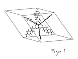
Fig.1 : die Anordnung der Atome im metallorganischen Framework IRMOF-10. -
Fig.1 zeigt den atomaren Aufbau des metallorganischen Frameworks IRMOF-10. Die Koordinaten der 166 Atome der Elementarzelle sind in Tabelle 1 angegeben. -
0.000000 17.674087 17.674087 17.674087 0.000000 17.674087 17.674087 17.674087 0.000000 - Die Eigenschaften dieses IRMOF-10 sind folgende;
- Dielektrizitätskonstante k = 1,23
Mechanischer Kompressionsmodul B = 6,00 GPa
Energiebandlücke Eg = 3,07 eV. - Die nachfolgenden metallorganischen Frameworks zeigen die dazu aufgeführten Eigenschaften:
IRMOF-1, FCC k = 1,37 B = 8,7 GPa Eg = 3,73 IRMOF-1, SC k = 1,39 B = 6,33 GPa Eg = 3,66 IRMOF-M11 k = 1,45 B = 12,00 GPa Eg = 4,91 IRMOF-M13 k = 1,50 B = 9,00 GPa Eg = 5,49 IRMOF-14 k = 1,28 B = 5,90 GPa Eg = 2,63 - Das kovalente organische Framework COF-108 zeigt die nachfolgenden Eigenschaften: Massendichte: 0,17 g/cm3 und spezifische Oberfläche (BET): 4210 m2/g (H. M. EI-Kalderi u.a. Science 316 (2007) 268-272) sowie k = 1,4.
| Koordinaten der Atome von IRMOF-10. Atomsorte, x-,y-,z-Koordinaten sowie Transformationsmatrix. | |||
| C | 17.69545500 | 31.52594000 | 17.64974900 |
| C | 17.65012100 | 17.65330200 | 3.82251600 |
| C | 17.68594600 | 3.80991400 | 17.65938200 |
| C | 17.65899300 | 17.66272200 | 31.53854200 |
| C | 3.82249800 | 17.69872400 | 17.69584300 |
| C | 31.53852400 | 17.68905700 | 17.68559300 |
| O | 32.18758700 | 16.66136200 | 18.18911000 |
| O | 32.19274800 | 18.72468700 | 17.19541900 |
| O | 17.04497800 | 32.17148600 | 18.59328100 |
| O | 18.34957300 | 32.17146800 | 16.70818000 |
| O | 18.59389900 | 18.30374400 | 3.17728800 |
| O | 16.70839200 | 16.99962600 | 3.17677600 |
| O | 17.66837800 | 0.00825400 | 17.66836000 |
| O | 17.19619700 | 3.15569100 | 16.62350400 |
| O | 18.18914500 | 3.16101000 | 18.68727100 |
| O | 16.62325600 | 18.15298400 | 32.19257100 |
| O | 18.68661700 | 17.15934700 | 32.18774600 |
| O | 3.17689900 | 16.75487500 | 17.04580800 |
| O | 3.17712900 | 18.64045300 | 18.34985500 |
| Zn | 16.47421100 | 16.47901800 | 1.18434100 |
| Zn | 16.46673400 | 1.20790000 | 16.46654000 |
| Zn | 1.19556400 | 16.49004700 | 16.47437000 |
| Zn | 1.18405800 | 1.19996400 | 1.19529800 |
| C | 5.98969500 | 16.75332000 | 16.93237600 |
| C | 5.27866600 | 17.69865400 | 17.69273300 |
| C | 7.38055700 | 16.75989500 | 16.92475800 |
| C | 5.99116200 | 18.64469400 | 18.45158700 |
| C | 8.10432900 | 17.69861800 | 17.69071800 |
| C | 7.38165300 | 18.63778400 | 18.45666000 |
| C | 10.30234900 | 16.60814500 | 17.16288100 |
| C | 9.57861300 | 17.69808800 | 17.69105400 |
| C | 11.69333500 | 16.61196200 | 17.15400900 |
| C | 10.30174800 | 18.78826100 | 18.22087000 |
| C | 11.69231000 | 18.78463800 | 18.23142100 |
| C | 12.40604200 | 17.69845900 | 17.69294500 |
| H | 5.44004900 | 16.01298800 | 16.33879200 |
| H | 5.44162200 | 19.38442600 | 19.04534800 |
| H | 12.24167300 | 15.76320000 | 16.72732100 |
| H | 12.24064800 | 19.63258800 | 18.65927600 |
| H | 9.77366400 | 19.65839200 | 18.62594200 |
| H | 7.90924200 | 19.37283200 | 19.07465200 |
| H | 7.90759800 | 16.02543000 | 16.30556400 |
| H | 9.77467100 | 15.73720100 | 16.75825100 |
| C | 18.21282800 | 5.97857800 | 18.75439800 |
| C | 17.67679100 | 5.26680700 | 17.66547900 |
| C | 18.20233000 | 7.36944000 | 18.76081300 |
| C | 17.13619400 | 5.98126400 | 16.58112100 |
| C | 17.67424600 | 8.09390100 | 17.67087000 |
| C | 17.14460600 | 7.37195000 | 16.58000800 |
| C | 18.44144200 | 10.29241600 | 18.60833900 |
| C | 17.67507600 | 9.56837900 | 17.67067600 |
| C | 18.43642300 | 11.68308400 | 18.61229800 |
| C | 16.90917000 | 10.29093100 | 16.73159800 |
| C | 16.91634600 | 11.68144000 | 16.72231900 |
| C | 17.67801000 | 12.39383000 | 17.66519700 |
| H | 18.63930400 | 5.42937300 | 19.60261200 |
| H | 16.70961200 | 5.43329700 | 15.73237600 |
| H | 19.03136800 | 12.23301300 | 19.35162300 |
| H | 16.32193100 | 12.23025600 | 15.98195200 |
| H | 16.29052400 | 9.76272400 | 15.99697500 |
| H | 16.73965800 | 7.90056400 | 15.71035400 |
| H | 18.60681900 | 7.89632200 | 19.63191600 |
| H | 19.06070700 | 9.76532200 | 19.34335100 |
| C | 18.59529500 | 18.41583300 | 5.98992500 |
| C | 17.64994400 | 17.65572300 | 5.27866600 |
| C | 18.58852600 | 18.42322100 | 7.38078700 |
| C | 16.70392100 | 16.89662100 | 5.99093200 |
| C | 17.64964300 | 17.65736700 | 8.10432900 |
| C | 16.71061900 | 16.89131900 | 7.38144100 |
| C | 18.74001100 | 18.18564500 | 10.30219000 |
| C | 17.65001500 | 17.65724300 | 9.57863000 |
| C | 18.73642300 | 18.19457100 | 11.69317600 |
| C | 16.55991200 | 17.12765700 | 10.30188900 |
| C | 16.56373000 | 17.11715900 | 11.69248600 |
| C | 17.65010300 | 17.65551100 | 12.40600700 |
| H | 19.33573400 | 19.00941700 | 5.44045500 |
| H | 15.96427800 | 16.30286000 | 5.44123300 |
| H | 19.58522100 | 18.62140000 | 12.24130200 |
| H | 15.71581600 | 16.68948100 | 12.24100200 |
| H | 15.68962300 | 16.72269100 | 9.77396400 |
| H | 15.97564200 | 16.27323900 | 7.90897700 |
| H | 19.32306100 | 19.04230800 | 7.90786400 |
| H | 19.61081300 | 18.59040000 | 9.77438900 |
| C | 17.68523900 | 13.85089900 | 17.65876300 |
| C | 17.65005000 | 17.65264800 | 13.86335900 |
| C | 17.69557800 | 21.48497300 | 17.64976700 |
| C | 17.65846300 | 17.66300500 | 21.49746900 |
| C | 21.49748600 | 17.68987000 | 17.68516800 |
| C | 13.86335900 | 17.69888300 | 17.69557800 |
| O | 14.51544500 | 16.66553300 | 17.20307200 |
| O | 14.51487900 | 18.73052000 | 18.19262700 |
| O | 17.03997600 | 14.49833600 | 16.71109600 |
| O | 18.34207900 | 14.49425300 | 18.59798200 |
| O | 18.68363100 | 18.14497700 | 14.51532100 |
| O | 16.61860800 | 17.15551100 | 14.51502000 |
| O | 17.67005700 | 17.67845200 | 17.67007500 |
| O | 17.20321400 | 20.83297600 | 18.68327700 |
| O | 18.19264400 | 20.83334700 | 16.61821900 |
| O | 16.71079600 | 18.30833900 | 20.85006700 |
| O | 18.59764600 | 17.00614800 | 20.85409700 |
| O | 20.85404400 | 16.75072200 | 18.34206100 |
| O | 20.85012000 | 18.63755400 | 17.03985200 |
| Zn | 16.46371200 | 16.48216400 | 16.47726800 |
| Zn | 16.47709100 | 18.88477900 | 18.86622100 |
| Zn | 18.86307600 | 16.48522200 | 18.86311100 |
| Zn | 18.86627500 | 18.87111700 | 16.46351800 |
| C | 29.36717400 | 18.76728200 | 17.13619400 |
| C | 30.08164900 | 17.68287100 | 17.67661400 |
| C | 27.97648900 | 18.76836000 | 17.14478300 |
| C | 29.36996700 | 16.59395300 | 18.21277500 |
| C | 27.25455500 | 17.67744500 | 17.67438700 |
| C | 27.97910400 | 16.58757200 | 18.20241800 |
| C | 25.05759500 | 18.61671600 | 16.90917000 |
| C | 25.78007700 | 17.67767500 | 17.67514700 |
| C | 23.66706900 | 18.62610100 | 16.91625700 |
| C | 25.05591600 | 16.74001100 | 18.44142500 |
| C | 23.66524900 | 16.73612300 | 18.43633500 |
| C | 22.95457400 | 17.68327700 | 17.67794000 |
| H | 29.91507100 | 19.61604500 | 16.70959400 |
| H | 29.91922400 | 15.74573800 | 18.63916300 |
| H | 23.11832400 | 19.36648700 | 16.32178900 |
| H | 23.11523100 | 15.99679800 | 19.03119100 |
| H | 25.58292200 | 16.00491100 | 19.06068900 |
| H | 27.45225700 | 15.71650500 | 18.60697800 |
| H | 27.44792700 | 19.63806700 | 16.73997600 |
| H | 25.58583900 | 19.35125100 | 16.29047100 |
| C | 18.45162300 | 29.35740000 | 16.70376200 |
| C | 17.69262700 | 30.06980700 | 17.64978500 |
| C | 18.45681900 | 27.96690900 | 16.71061900 |
| C | 16.93244700 | 29.35869000 | 18.59517200 |
| C | 17.69087700 | 27.24411000 | 17.64976700 |
| C | 16.92500600 | 27.96781100 | 18.58854400 |
| C | 18.22079900 | 25.04660200 | 16.56008900 |
| C | 17.69112400 | 25.76980800 | 17.65019100 |
| C | 18.23126200 | 23.65598700 | 16.56374800 |
| C | 17.16279300 | 25.04612500 | 18.74013500 |
| C | 17.15383200 | 23.65512100 | 18.73638800 |
| C | 17.69280400 | 22.94234300 | 17.64999700 |
| H | 19.04534800 | 29.90701100 | 15.96403000 |
| H | 16.33888000 | 29.90823100 | 19.33562800 |
| H | 18.65901000 | 23.10756000 | 15.71578000 |
| H | 16.72703800 | 23.10687100 | 19.58516800 |
| H | 16.75810900 | 25.57382000 | 19.61104300 |
| H | 16.30590000 | 27.44080500 | 19.32306100 |
| H | 19.07482900 | 27.43937300 | 15.97564200 |
| H | 18.62594200 | 25.57456200 | 15.68990500 |
| C | 16.58103300 | 18.21217400 | 29.36712100 |
| C | 17.66537300 | 17.67164800 | 30.08163100 |
| C | 16.58000800 | 18.20365500 | 27.97645300 |
| C | 18.75432700 | 17.13552200 | 29.37002000 |
| C | 17.67095800 | 17.67406900 | 27.25457300 |
| C | 18.76077800 | 17.14596700 | 27.97914000 |
| C | 16.73172200 | 18.43926900 | 25.05756000 |
| C | 17.67079900 | 17.67332700 | 25.78007700 |
| C | 16.72224900 | 18.43202200 | 23.66703400 |
| C | 18.60842700 | 16.90701400 | 25.05595200 |
| C | 18.61224500 | 16.91194500 | 23.66526600 |
| C | 17.66502000 | 17.67025100 | 22.95457400 |
| H | 15.73227000 | 18.63877400 | 29.91501800 |
| H | 19.60252400 | 16.70908200 | 29.91927700 |
| H | 15.98184600 | 19.02643700 | 23.11828900 |
| H | 19.35149900 | 16.31701700 | 23.11528400 |
| H | 19.34363400 | 16.28790800 | 25.58297500 |
| H | 19.63188100 | 16.74142500 | 27.45234600 |
| H | 15.71035400 | 18.60849800 | 27.44783900 |
| H | 15.99724000 | 19.05807400 | 25.58578600 |
Claims (8)
- Integrierte Schaltkreise enthaltend Isolationsmaterial aus ausschließlich IRMOFs, die ein isoreticulares kubisches Netzwerk mit analogem Bauprinzip aufweisen, mit Dielektrizitätskonstanten von k ≤ 2, und vorzugsweise Haftvermittler, wie Parylene, gekennzeichnet dadurch, dass als Isolationsmaterial IRMOF-1 FCC, IRMOF-1 SC, IRMOF-10, IRMOF-M11, IRMOF-M13 und/oder IRMOF-14 verwendet wird.
- Isolationsmaterial nach Anspruch 1, bei dem IRMOFs in kristalliner bis ungeordneter, freier Form vorhanden sind.
- Isolationsmaterial nach Anspruch 1, bei dem als zentrales Atom im Netzwerk ein Metallatom vorhanden ist.
- Isolationsmaterial nach Anspruch 3, bei dem als Metallatom Cu oder Zn vorhanden ist.
- Verwendung von ausschließlich IRMOFs, die ein isoreticulares kubisches Netzwerk mit analogem Bauprinzip aufweisen, mit Dielektrizitätskonstanten von k ≤ 2 und vorzugsweise Haftvermittler, wie Parylene, in Form von IRMOF-1 FCC, IRMOF-1 SC, IRMOF-10, IRMOF-M11, IRMOF-M13 und/oder IRMOF-14 als Isolationsmaterial für integrierte Schaltkreise.
- Verwendung nach Anspruch 5 von IRMOFs in kristalliner bis ungeordneter, freier Form als Isolatormaterial mit Dielektrizitätskonstanten von k ≤ 2 für integrierte Schaltkreise.
- Verwendung nach Anspruch 5, von IRMOFs mit einem zentralen Metallatom im Netzwerk als Isolatormaterial mit Dielektrizitätskonstanten von k ≤ 2 für integrierte Schaltkreise.
- Verwendung nach Anspruch 5 von Cu oder Zn als Metallatom für Isolatormaterial mit Dielektrizitätskonstanten von k ≤ 2 für integrierte Schaltkreise.
Applications Claiming Priority (2)
| Application Number | Priority Date | Filing Date | Title |
|---|---|---|---|
| DE102009001044.0A DE102009001044B4 (de) | 2009-02-20 | 2009-02-20 | Isolationsmaterial für integrierte Schaltkreise |
| PCT/EP2010/051297 WO2010094562A1 (de) | 2009-02-20 | 2010-02-03 | Isolationsmaterial für integrierte schaltkreise und deren verwendung |
Publications (2)
| Publication Number | Publication Date |
|---|---|
| EP2399282A1 EP2399282A1 (de) | 2011-12-28 |
| EP2399282B1 true EP2399282B1 (de) | 2014-04-09 |
Family
ID=42194784
Family Applications (1)
| Application Number | Title | Priority Date | Filing Date |
|---|---|---|---|
| EP10704527.0A Not-in-force EP2399282B1 (de) | 2009-02-20 | 2010-02-03 | Integrierte schaltkreise enthaltend isolationsmaterial und dessen verwendung in integrierten schaltkreisen |
Country Status (4)
| Country | Link |
|---|---|
| US (1) | US9117771B2 (de) |
| EP (1) | EP2399282B1 (de) |
| DE (1) | DE102009001044B4 (de) |
| WO (1) | WO2010094562A1 (de) |
Families Citing this family (3)
| Publication number | Priority date | Publication date | Assignee | Title |
|---|---|---|---|---|
| KR102842040B1 (ko) | 2021-02-22 | 2025-08-04 | 에스케이하이닉스 주식회사 | 가변 저항 채널층을 구비하는 전자 장치 |
| KR20220142884A (ko) * | 2021-04-15 | 2022-10-24 | 에스케이하이닉스 주식회사 | 금속-유기물 구조체층을 포함하는 층간 절연 구조물을 구비하는 반도체 장치 |
| KR102916125B1 (ko) | 2021-07-13 | 2026-01-21 | 에스케이하이닉스 주식회사 | 금속-유기물 구조체층을 포함하는 층간 절연 구조물을 구비하는 반도체 장치 |
Family Cites Families (2)
| Publication number | Priority date | Publication date | Assignee | Title |
|---|---|---|---|---|
| DE10111230A1 (de) * | 2001-03-08 | 2002-09-19 | Basf Ag | Metallorganische Gerüstmaterialien und Verfahren zu deren Herstellung |
| DE10253855A1 (de) | 2002-11-14 | 2004-06-03 | Leibniz-Institut für Festkörper- und Werkstoffforschung e.V. | Isolationsschichtmaterial für integrierte Schaltkreise in Damascene-Architektur |
-
2009
- 2009-02-20 DE DE102009001044.0A patent/DE102009001044B4/de not_active Expired - Fee Related
-
2010
- 2010-02-03 EP EP10704527.0A patent/EP2399282B1/de not_active Not-in-force
- 2010-02-03 US US13/202,228 patent/US9117771B2/en not_active Expired - Fee Related
- 2010-02-03 WO PCT/EP2010/051297 patent/WO2010094562A1/de not_active Ceased
Also Published As
| Publication number | Publication date |
|---|---|
| EP2399282A1 (de) | 2011-12-28 |
| WO2010094562A1 (de) | 2010-08-26 |
| DE102009001044B4 (de) | 2015-08-13 |
| US9117771B2 (en) | 2015-08-25 |
| DE102009001044A1 (de) | 2010-09-02 |
| US20110297869A1 (en) | 2011-12-08 |
Similar Documents
| Publication | Publication Date | Title |
|---|---|---|
| DE69535718T2 (de) | Verbindungsverfahren mit Benutzung eines porösen Isolators zur Reduzierung der Kapazitäten zwischen Leiterbahnen | |
| DE69524665T2 (de) | Verfahren zur Herstellung einer porösen dielektrischen Schicht für eine Halbleiteranordnung | |
| DE102020105731B4 (de) | Kondensator, metall-isolator-metallstruktur und verfahren zu ihrer herstellung | |
| DE102013221775A1 (de) | Ein Bulk Akustik Wave Resonator, welcher eine dotierte piezoelektrische Schicht mit verbesserten piezoelektrischen Charakteristiken hat | |
| EP2847775B1 (de) | Keramischer vielschichtkondensator | |
| DE20221998U1 (de) | Kugelaktivkohle | |
| DE102009001044B4 (de) | Isolationsmaterial für integrierte Schaltkreise | |
| DE112007001286T5 (de) | Kohlenstoff und Kohlenstoffverbundstoffe mit hochgeordneten Poren mit Mesogrösse | |
| DE112009000012T5 (de) | Glaskeramikzusammensetzung, Glaskeramik-Sinterkörper und keramisches Mehrschicht-Elektronikbauteil | |
| DE60203394T2 (de) | Träger mit integrierter abscheidung von gasabsorbierendem material zur herstellung von mikroelektronischen, microoptoelektronischen oder mikromechanischen bauelementen | |
| DE102013102278A1 (de) | Kondensatoranordnung | |
| DE112004001324T5 (de) | Filme mit niedriger Dielektrizitätskonstante und Herstellungsverfahren für diese Filme sowie elektronische Bauteile, die diese Filme verwenden | |
| DE3601283A1 (de) | Materialien zur gastrennung | |
| DE112017004718T5 (de) | Verbundsubstrat, Verfahren zu seiner Herstellung und elektronische Vorrichtung | |
| DE102010056572A1 (de) | Elektronisches Bauelement und Verfahren zur Herstellung des elektronischen Bauelements | |
| DE112004002266B4 (de) | Dielektrischer Film mit sehr geringer Dielektrizitätskonstante für Kupferverbindungen | |
| DE102017116925B4 (de) | Harte PZT-Keramik, piezoelektrisches Vielschichtbauelement und Verfahren zur Herstellung eines piezoelektrischen Vielschichtbauelements | |
| DE112023003019T5 (de) | Dünnschichtpolymerlaminierter kondensator und herstellungsverfahren für diesen | |
| EP2537168B1 (de) | Doppelschichtkondensator | |
| DE102004037601B4 (de) | Elektrolytlösung für Doppelschichtkondensatoren und Doppelschichtkondensator mit der Elektrolytlösung | |
| DE10016427A1 (de) | Sensor, insbesondere Feuchtesensor, und Verfahren zur Herstellung desselben | |
| DE2204946A1 (de) | Dünnschicht-MOM-Kondensator und Verfahren zu seiner Herstellung | |
| DE10136545B4 (de) | Elektrokeramisches Bauelement, Vielschichtkondensator und Verfahren zur Herstellung des Vielschichtkondensators | |
| EP1420447B1 (de) | Isolationsschichtmaterial für integrierte Schaltkreise in Damascene-Architektur, bestehend aus Molekülen die nur auf der Oberfläche mit Atomen besetzt sind, wie z.B. Fullerenen | |
| EP3557633A1 (de) | Hochvolt-kondensator zur integration in elektrische leistungsmodule sowie verfahren zur herstellung |
Legal Events
| Date | Code | Title | Description |
|---|---|---|---|
| PUAI | Public reference made under article 153(3) epc to a published international application that has entered the european phase |
Free format text: ORIGINAL CODE: 0009012 |
|
| 17P | Request for examination filed |
Effective date: 20110919 |
|
| AK | Designated contracting states |
Kind code of ref document: A1 Designated state(s): AT BE BG CH CY CZ DE DK EE ES FI FR GB GR HR HU IE IS IT LI LT LU LV MC MK MT NL NO PL PT RO SE SI SK SM TR |
|
| DAX | Request for extension of the european patent (deleted) | ||
| 17Q | First examination report despatched |
Effective date: 20120809 |
|
| GRAP | Despatch of communication of intention to grant a patent |
Free format text: ORIGINAL CODE: EPIDOSNIGR1 |
|
| INTG | Intention to grant announced |
Effective date: 20130828 |
|
| GRAS | Grant fee paid |
Free format text: ORIGINAL CODE: EPIDOSNIGR3 |
|
| GRAA | (expected) grant |
Free format text: ORIGINAL CODE: 0009210 |
|
| AK | Designated contracting states |
Kind code of ref document: B1 Designated state(s): AT BE BG CH CY CZ DE DK EE ES FI FR GB GR HR HU IE IS IT LI LT LU LV MC MK MT NL NO PL PT RO SE SI SK SM TR |
|
| REG | Reference to a national code |
Ref country code: GB Ref legal event code: FG4D Free format text: NOT ENGLISH |
|
| REG | Reference to a national code |
Ref country code: CH Ref legal event code: EP Ref country code: AT Ref legal event code: REF Ref document number: 661748 Country of ref document: AT Kind code of ref document: T Effective date: 20140415 |
|
| REG | Reference to a national code |
Ref country code: IE Ref legal event code: FG4D Free format text: LANGUAGE OF EP DOCUMENT: GERMAN |
|
| REG | Reference to a national code |
Ref country code: DE Ref legal event code: R096 Ref document number: 502010006598 Country of ref document: DE Effective date: 20140522 |
|
| REG | Reference to a national code |
Ref country code: NL Ref legal event code: VDEP Effective date: 20140409 |
|
| REG | Reference to a national code |
Ref country code: LT Ref legal event code: MG4D |
|
| PG25 | Lapsed in a contracting state [announced via postgrant information from national office to epo] |
Ref country code: BG Free format text: LAPSE BECAUSE OF FAILURE TO SUBMIT A TRANSLATION OF THE DESCRIPTION OR TO PAY THE FEE WITHIN THE PRESCRIBED TIME-LIMIT Effective date: 20140709 Ref country code: LT Free format text: LAPSE BECAUSE OF FAILURE TO SUBMIT A TRANSLATION OF THE DESCRIPTION OR TO PAY THE FEE WITHIN THE PRESCRIBED TIME-LIMIT Effective date: 20140409 Ref country code: FI Free format text: LAPSE BECAUSE OF FAILURE TO SUBMIT A TRANSLATION OF THE DESCRIPTION OR TO PAY THE FEE WITHIN THE PRESCRIBED TIME-LIMIT Effective date: 20140409 Ref country code: IS Free format text: LAPSE BECAUSE OF FAILURE TO SUBMIT A TRANSLATION OF THE DESCRIPTION OR TO PAY THE FEE WITHIN THE PRESCRIBED TIME-LIMIT Effective date: 20140809 Ref country code: NO Free format text: LAPSE BECAUSE OF FAILURE TO SUBMIT A TRANSLATION OF THE DESCRIPTION OR TO PAY THE FEE WITHIN THE PRESCRIBED TIME-LIMIT Effective date: 20140709 Ref country code: NL Free format text: LAPSE BECAUSE OF FAILURE TO SUBMIT A TRANSLATION OF THE DESCRIPTION OR TO PAY THE FEE WITHIN THE PRESCRIBED TIME-LIMIT Effective date: 20140409 Ref country code: GR Free format text: LAPSE BECAUSE OF FAILURE TO SUBMIT A TRANSLATION OF THE DESCRIPTION OR TO PAY THE FEE WITHIN THE PRESCRIBED TIME-LIMIT Effective date: 20140710 |
|
| PG25 | Lapsed in a contracting state [announced via postgrant information from national office to epo] |
Ref country code: SE Free format text: LAPSE BECAUSE OF FAILURE TO SUBMIT A TRANSLATION OF THE DESCRIPTION OR TO PAY THE FEE WITHIN THE PRESCRIBED TIME-LIMIT Effective date: 20140409 Ref country code: PL Free format text: LAPSE BECAUSE OF FAILURE TO SUBMIT A TRANSLATION OF THE DESCRIPTION OR TO PAY THE FEE WITHIN THE PRESCRIBED TIME-LIMIT Effective date: 20140409 Ref country code: LV Free format text: LAPSE BECAUSE OF FAILURE TO SUBMIT A TRANSLATION OF THE DESCRIPTION OR TO PAY THE FEE WITHIN THE PRESCRIBED TIME-LIMIT Effective date: 20140409 Ref country code: HR Free format text: LAPSE BECAUSE OF FAILURE TO SUBMIT A TRANSLATION OF THE DESCRIPTION OR TO PAY THE FEE WITHIN THE PRESCRIBED TIME-LIMIT Effective date: 20140409 Ref country code: ES Free format text: LAPSE BECAUSE OF FAILURE TO SUBMIT A TRANSLATION OF THE DESCRIPTION OR TO PAY THE FEE WITHIN THE PRESCRIBED TIME-LIMIT Effective date: 20140409 |
|
| PG25 | Lapsed in a contracting state [announced via postgrant information from national office to epo] |
Ref country code: PT Free format text: LAPSE BECAUSE OF FAILURE TO SUBMIT A TRANSLATION OF THE DESCRIPTION OR TO PAY THE FEE WITHIN THE PRESCRIBED TIME-LIMIT Effective date: 20140811 |
|
| REG | Reference to a national code |
Ref country code: DE Ref legal event code: R097 Ref document number: 502010006598 Country of ref document: DE |
|
| PG25 | Lapsed in a contracting state [announced via postgrant information from national office to epo] |
Ref country code: RO Free format text: LAPSE BECAUSE OF FAILURE TO SUBMIT A TRANSLATION OF THE DESCRIPTION OR TO PAY THE FEE WITHIN THE PRESCRIBED TIME-LIMIT Effective date: 20140409 Ref country code: SK Free format text: LAPSE BECAUSE OF FAILURE TO SUBMIT A TRANSLATION OF THE DESCRIPTION OR TO PAY THE FEE WITHIN THE PRESCRIBED TIME-LIMIT Effective date: 20140409 Ref country code: CZ Free format text: LAPSE BECAUSE OF FAILURE TO SUBMIT A TRANSLATION OF THE DESCRIPTION OR TO PAY THE FEE WITHIN THE PRESCRIBED TIME-LIMIT Effective date: 20140409 Ref country code: DK Free format text: LAPSE BECAUSE OF FAILURE TO SUBMIT A TRANSLATION OF THE DESCRIPTION OR TO PAY THE FEE WITHIN THE PRESCRIBED TIME-LIMIT Effective date: 20140409 Ref country code: EE Free format text: LAPSE BECAUSE OF FAILURE TO SUBMIT A TRANSLATION OF THE DESCRIPTION OR TO PAY THE FEE WITHIN THE PRESCRIBED TIME-LIMIT Effective date: 20140409 |
|
| PLBE | No opposition filed within time limit |
Free format text: ORIGINAL CODE: 0009261 |
|
| STAA | Information on the status of an ep patent application or granted ep patent |
Free format text: STATUS: NO OPPOSITION FILED WITHIN TIME LIMIT |
|
| 26N | No opposition filed |
Effective date: 20150112 |
|
| PG25 | Lapsed in a contracting state [announced via postgrant information from national office to epo] |
Ref country code: IT Free format text: LAPSE BECAUSE OF FAILURE TO SUBMIT A TRANSLATION OF THE DESCRIPTION OR TO PAY THE FEE WITHIN THE PRESCRIBED TIME-LIMIT Effective date: 20140409 |
|
| REG | Reference to a national code |
Ref country code: DE Ref legal event code: R097 Ref document number: 502010006598 Country of ref document: DE Effective date: 20150112 |
|
| PG25 | Lapsed in a contracting state [announced via postgrant information from national office to epo] |
Ref country code: BE Free format text: LAPSE BECAUSE OF NON-PAYMENT OF DUE FEES Effective date: 20150228 |
|
| PG25 | Lapsed in a contracting state [announced via postgrant information from national office to epo] |
Ref country code: SI Free format text: LAPSE BECAUSE OF FAILURE TO SUBMIT A TRANSLATION OF THE DESCRIPTION OR TO PAY THE FEE WITHIN THE PRESCRIBED TIME-LIMIT Effective date: 20140409 |
|
| PG25 | Lapsed in a contracting state [announced via postgrant information from national office to epo] |
Ref country code: LU Free format text: LAPSE BECAUSE OF FAILURE TO SUBMIT A TRANSLATION OF THE DESCRIPTION OR TO PAY THE FEE WITHIN THE PRESCRIBED TIME-LIMIT Effective date: 20150203 |
|
| PG25 | Lapsed in a contracting state [announced via postgrant information from national office to epo] |
Ref country code: MC Free format text: LAPSE BECAUSE OF FAILURE TO SUBMIT A TRANSLATION OF THE DESCRIPTION OR TO PAY THE FEE WITHIN THE PRESCRIBED TIME-LIMIT Effective date: 20140409 |
|
| REG | Reference to a national code |
Ref country code: IE Ref legal event code: MM4A |
|
| PG25 | Lapsed in a contracting state [announced via postgrant information from national office to epo] |
Ref country code: IE Free format text: LAPSE BECAUSE OF NON-PAYMENT OF DUE FEES Effective date: 20150203 |
|
| REG | Reference to a national code |
Ref country code: FR Ref legal event code: PLFP Year of fee payment: 7 |
|
| PG25 | Lapsed in a contracting state [announced via postgrant information from national office to epo] |
Ref country code: MT Free format text: LAPSE BECAUSE OF FAILURE TO SUBMIT A TRANSLATION OF THE DESCRIPTION OR TO PAY THE FEE WITHIN THE PRESCRIBED TIME-LIMIT Effective date: 20140409 |
|
| REG | Reference to a national code |
Ref country code: FR Ref legal event code: PLFP Year of fee payment: 8 |
|
| PG25 | Lapsed in a contracting state [announced via postgrant information from national office to epo] |
Ref country code: HU Free format text: LAPSE BECAUSE OF FAILURE TO SUBMIT A TRANSLATION OF THE DESCRIPTION OR TO PAY THE FEE WITHIN THE PRESCRIBED TIME-LIMIT; INVALID AB INITIO Effective date: 20100203 Ref country code: SM Free format text: LAPSE BECAUSE OF FAILURE TO SUBMIT A TRANSLATION OF THE DESCRIPTION OR TO PAY THE FEE WITHIN THE PRESCRIBED TIME-LIMIT Effective date: 20140409 |
|
| PG25 | Lapsed in a contracting state [announced via postgrant information from national office to epo] |
Ref country code: CY Free format text: LAPSE BECAUSE OF FAILURE TO SUBMIT A TRANSLATION OF THE DESCRIPTION OR TO PAY THE FEE WITHIN THE PRESCRIBED TIME-LIMIT Effective date: 20140409 |
|
| PG25 | Lapsed in a contracting state [announced via postgrant information from national office to epo] |
Ref country code: TR Free format text: LAPSE BECAUSE OF FAILURE TO SUBMIT A TRANSLATION OF THE DESCRIPTION OR TO PAY THE FEE WITHIN THE PRESCRIBED TIME-LIMIT Effective date: 20140409 |
|
| REG | Reference to a national code |
Ref country code: FR Ref legal event code: PLFP Year of fee payment: 9 |
|
| PG25 | Lapsed in a contracting state [announced via postgrant information from national office to epo] |
Ref country code: MK Free format text: LAPSE BECAUSE OF FAILURE TO SUBMIT A TRANSLATION OF THE DESCRIPTION OR TO PAY THE FEE WITHIN THE PRESCRIBED TIME-LIMIT Effective date: 20140409 |
|
| PGFP | Annual fee paid to national office [announced via postgrant information from national office to epo] |
Ref country code: CH Payment date: 20210324 Year of fee payment: 12 Ref country code: FR Payment date: 20210317 Year of fee payment: 12 |
|
| PGFP | Annual fee paid to national office [announced via postgrant information from national office to epo] |
Ref country code: GB Payment date: 20210324 Year of fee payment: 12 Ref country code: DE Payment date: 20210323 Year of fee payment: 12 Ref country code: AT Payment date: 20210318 Year of fee payment: 12 |
|
| REG | Reference to a national code |
Ref country code: DE Ref legal event code: R119 Ref document number: 502010006598 Country of ref document: DE |
|
| REG | Reference to a national code |
Ref country code: CH Ref legal event code: PL |
|
| REG | Reference to a national code |
Ref country code: AT Ref legal event code: MM01 Ref document number: 661748 Country of ref document: AT Kind code of ref document: T Effective date: 20220203 |
|
| GBPC | Gb: european patent ceased through non-payment of renewal fee |
Effective date: 20220203 |
|
| PG25 | Lapsed in a contracting state [announced via postgrant information from national office to epo] |
Ref country code: AT Free format text: LAPSE BECAUSE OF NON-PAYMENT OF DUE FEES Effective date: 20220203 |
|
| PG25 | Lapsed in a contracting state [announced via postgrant information from national office to epo] |
Ref country code: FR Free format text: LAPSE BECAUSE OF NON-PAYMENT OF DUE FEES Effective date: 20220228 |
|
| PG25 | Lapsed in a contracting state [announced via postgrant information from national office to epo] |
Ref country code: LI Free format text: LAPSE BECAUSE OF NON-PAYMENT OF DUE FEES Effective date: 20220228 Ref country code: GB Free format text: LAPSE BECAUSE OF NON-PAYMENT OF DUE FEES Effective date: 20220203 Ref country code: DE Free format text: LAPSE BECAUSE OF NON-PAYMENT OF DUE FEES Effective date: 20220901 Ref country code: CH Free format text: LAPSE BECAUSE OF NON-PAYMENT OF DUE FEES Effective date: 20220228 |