EP2394816A1 - Verfahren für markierung, verschlüsselung, etikettierung und optische kodierung - Google Patents
Verfahren für markierung, verschlüsselung, etikettierung und optische kodierung Download PDFInfo
- Publication number
- EP2394816A1 EP2394816A1 EP10738235A EP10738235A EP2394816A1 EP 2394816 A1 EP2394816 A1 EP 2394816A1 EP 10738235 A EP10738235 A EP 10738235A EP 10738235 A EP10738235 A EP 10738235A EP 2394816 A1 EP2394816 A1 EP 2394816A1
- Authority
- EP
- European Patent Office
- Prior art keywords
- process according
- motifs
- marking
- substrate
- layer
- Prior art date
- Legal status (The legal status is an assumption and is not a legal conclusion. Google has not performed a legal analysis and makes no representation as to the accuracy of the status listed.)
- Granted
Links
- 238000000034 method Methods 0.000 title claims abstract description 100
- 230000003287 optical effect Effects 0.000 title claims abstract description 20
- 238000002372 labelling Methods 0.000 title claims description 6
- 229920001109 fluorescent polymer Polymers 0.000 claims abstract description 13
- 239000000758 substrate Substances 0.000 claims description 32
- 230000008021 deposition Effects 0.000 claims description 15
- 238000006116 polymerization reaction Methods 0.000 claims description 14
- 238000002679 ablation Methods 0.000 claims description 9
- 238000005299 abrasion Methods 0.000 claims description 7
- 239000011521 glass Substances 0.000 claims description 3
- 230000001066 destructive effect Effects 0.000 claims description 2
- 230000005284 excitation Effects 0.000 claims description 2
- 239000000919 ceramic Substances 0.000 claims 1
- 238000005286 illumination Methods 0.000 claims 1
- 239000002184 metal Substances 0.000 claims 1
- 229920000642 polymer Polymers 0.000 abstract description 7
- 230000000007 visual effect Effects 0.000 abstract description 4
- 238000013532 laser treatment Methods 0.000 abstract description 2
- 238000011282 treatment Methods 0.000 abstract description 2
- 239000010410 layer Substances 0.000 description 78
- 239000000463 material Substances 0.000 description 15
- 239000000975 dye Substances 0.000 description 10
- HVQAJTFOCKOKIN-UHFFFAOYSA-N flavonol Chemical compound O1C2=CC=CC=C2C(=O)C(O)=C1C1=CC=CC=C1 HVQAJTFOCKOKIN-UHFFFAOYSA-N 0.000 description 10
- 230000005291 magnetic effect Effects 0.000 description 6
- 238000000608 laser ablation Methods 0.000 description 5
- 238000005137 deposition process Methods 0.000 description 4
- 238000001514 detection method Methods 0.000 description 4
- ZZLQHXCRRMUGQJ-UHFFFAOYSA-N 2'-Hydroxyflavone Natural products OC1=CC=CC=C1C1=CC(=O)C2=CC=CC=C2O1 ZZLQHXCRRMUGQJ-UHFFFAOYSA-N 0.000 description 3
- 238000010330 laser marking Methods 0.000 description 3
- 238000004519 manufacturing process Methods 0.000 description 3
- XKRFYHLGVUSROY-UHFFFAOYSA-N Argon Chemical compound [Ar] XKRFYHLGVUSROY-UHFFFAOYSA-N 0.000 description 2
- 238000011161 development Methods 0.000 description 2
- 238000001493 electron microscopy Methods 0.000 description 2
- 238000002189 fluorescence spectrum Methods 0.000 description 2
- 239000007789 gas Substances 0.000 description 2
- 238000010348 incorporation Methods 0.000 description 2
- 230000010354 integration Effects 0.000 description 2
- 239000000049 pigment Substances 0.000 description 2
- 238000002360 preparation method Methods 0.000 description 2
- 239000010453 quartz Substances 0.000 description 2
- VYPSYNLAJGMNEJ-UHFFFAOYSA-N silicon dioxide Inorganic materials O=[Si]=O VYPSYNLAJGMNEJ-UHFFFAOYSA-N 0.000 description 2
- 238000001228 spectrum Methods 0.000 description 2
- 239000000126 substance Substances 0.000 description 2
- XUIMIQQOPSSXEZ-UHFFFAOYSA-N Silicon Chemical compound [Si] XUIMIQQOPSSXEZ-UHFFFAOYSA-N 0.000 description 1
- 238000010521 absorption reaction Methods 0.000 description 1
- 238000000862 absorption spectrum Methods 0.000 description 1
- 239000002390 adhesive tape Substances 0.000 description 1
- 229910052786 argon Inorganic materials 0.000 description 1
- QVGXLLKOCUKJST-UHFFFAOYSA-N atomic oxygen Chemical compound [O] QVGXLLKOCUKJST-UHFFFAOYSA-N 0.000 description 1
- 230000001427 coherent effect Effects 0.000 description 1
- 239000003086 colorant Substances 0.000 description 1
- 230000000295 complement effect Effects 0.000 description 1
- 150000001875 compounds Chemical class 0.000 description 1
- 230000000593 degrading effect Effects 0.000 description 1
- 230000000694 effects Effects 0.000 description 1
- 230000008030 elimination Effects 0.000 description 1
- 238000003379 elimination reaction Methods 0.000 description 1
- 230000005294 ferromagnetic effect Effects 0.000 description 1
- 239000005357 flat glass Substances 0.000 description 1
- 239000007850 fluorescent dye Substances 0.000 description 1
- 239000000976 ink Substances 0.000 description 1
- 230000003993 interaction Effects 0.000 description 1
- 239000000696 magnetic material Substances 0.000 description 1
- 239000011159 matrix material Substances 0.000 description 1
- 239000002923 metal particle Substances 0.000 description 1
- 238000000399 optical microscopy Methods 0.000 description 1
- 239000001301 oxygen Substances 0.000 description 1
- 229910052760 oxygen Inorganic materials 0.000 description 1
- 238000002161 passivation Methods 0.000 description 1
- 239000013047 polymeric layer Substances 0.000 description 1
- 238000012545 processing Methods 0.000 description 1
- 229910052710 silicon Inorganic materials 0.000 description 1
- 239000010703 silicon Substances 0.000 description 1
- 238000005549 size reduction Methods 0.000 description 1
- 238000003980 solgel method Methods 0.000 description 1
- 238000000859 sublimation Methods 0.000 description 1
- 230000008022 sublimation Effects 0.000 description 1
Images


Classifications
-
- B—PERFORMING OPERATIONS; TRANSPORTING
- B41—PRINTING; LINING MACHINES; TYPEWRITERS; STAMPS
- B41C—PROCESSES FOR THE MANUFACTURE OR REPRODUCTION OF PRINTING SURFACES
- B41C1/00—Forme preparation
- B41C1/10—Forme preparation for lithographic printing; Master sheets for transferring a lithographic image to the forme
- B41C1/1008—Forme preparation for lithographic printing; Master sheets for transferring a lithographic image to the forme by removal or destruction of lithographic material on the lithographic support, e.g. by laser or spark ablation; by the use of materials rendered soluble or insoluble by heat exposure, e.g. by heat produced from a light to heat transforming system; by on-the-press exposure or on-the-press development, e.g. by the fountain of photolithographic materials
- B41C1/1033—Forme preparation for lithographic printing; Master sheets for transferring a lithographic image to the forme by removal or destruction of lithographic material on the lithographic support, e.g. by laser or spark ablation; by the use of materials rendered soluble or insoluble by heat exposure, e.g. by heat produced from a light to heat transforming system; by on-the-press exposure or on-the-press development, e.g. by the fountain of photolithographic materials by laser or spark ablation
-
- B—PERFORMING OPERATIONS; TRANSPORTING
- B41—PRINTING; LINING MACHINES; TYPEWRITERS; STAMPS
- B41M—PRINTING, DUPLICATING, MARKING, OR COPYING PROCESSES; COLOUR PRINTING
- B41M5/00—Duplicating or marking methods; Sheet materials for use therein
- B41M5/26—Thermography ; Marking by high energetic means, e.g. laser otherwise than by burning, and characterised by the material used
-
- B—PERFORMING OPERATIONS; TRANSPORTING
- B23—MACHINE TOOLS; METAL-WORKING NOT OTHERWISE PROVIDED FOR
- B23K—SOLDERING OR UNSOLDERING; WELDING; CLADDING OR PLATING BY SOLDERING OR WELDING; CUTTING BY APPLYING HEAT LOCALLY, e.g. FLAME CUTTING; WORKING BY LASER BEAM
- B23K26/00—Working by laser beam, e.g. welding, cutting or boring
- B23K26/009—Working by laser beam, e.g. welding, cutting or boring using a non-absorbing, e.g. transparent, reflective or refractive, layer on the workpiece
-
- B—PERFORMING OPERATIONS; TRANSPORTING
- B23—MACHINE TOOLS; METAL-WORKING NOT OTHERWISE PROVIDED FOR
- B23K—SOLDERING OR UNSOLDERING; WELDING; CLADDING OR PLATING BY SOLDERING OR WELDING; CUTTING BY APPLYING HEAT LOCALLY, e.g. FLAME CUTTING; WORKING BY LASER BEAM
- B23K26/00—Working by laser beam, e.g. welding, cutting or boring
- B23K26/02—Positioning or observing the workpiece, e.g. with respect to the point of impact; Aligning, aiming or focusing the laser beam
- B23K26/06—Shaping the laser beam, e.g. by masks or multi-focusing
- B23K26/064—Shaping the laser beam, e.g. by masks or multi-focusing by means of optical elements, e.g. lenses, mirrors or prisms
- B23K26/066—Shaping the laser beam, e.g. by masks or multi-focusing by means of optical elements, e.g. lenses, mirrors or prisms by using masks
- B23K26/0661—Shaping the laser beam, e.g. by masks or multi-focusing by means of optical elements, e.g. lenses, mirrors or prisms by using masks disposed on the workpiece
-
- B—PERFORMING OPERATIONS; TRANSPORTING
- B23—MACHINE TOOLS; METAL-WORKING NOT OTHERWISE PROVIDED FOR
- B23K—SOLDERING OR UNSOLDERING; WELDING; CLADDING OR PLATING BY SOLDERING OR WELDING; CUTTING BY APPLYING HEAT LOCALLY, e.g. FLAME CUTTING; WORKING BY LASER BEAM
- B23K26/00—Working by laser beam, e.g. welding, cutting or boring
- B23K26/08—Devices involving relative movement between laser beam and workpiece
- B23K26/083—Devices involving movement of the workpiece in at least one axial direction
- B23K26/0853—Devices involving movement of the workpiece in at least in two axial directions, e.g. in a plane
-
- B—PERFORMING OPERATIONS; TRANSPORTING
- B23—MACHINE TOOLS; METAL-WORKING NOT OTHERWISE PROVIDED FOR
- B23K—SOLDERING OR UNSOLDERING; WELDING; CLADDING OR PLATING BY SOLDERING OR WELDING; CUTTING BY APPLYING HEAT LOCALLY, e.g. FLAME CUTTING; WORKING BY LASER BEAM
- B23K26/00—Working by laser beam, e.g. welding, cutting or boring
- B23K26/08—Devices involving relative movement between laser beam and workpiece
- B23K26/0869—Devices involving movement of the laser head in at least one axial direction
- B23K26/0876—Devices involving movement of the laser head in at least one axial direction in at least two axial directions
-
- B—PERFORMING OPERATIONS; TRANSPORTING
- B23—MACHINE TOOLS; METAL-WORKING NOT OTHERWISE PROVIDED FOR
- B23K—SOLDERING OR UNSOLDERING; WELDING; CLADDING OR PLATING BY SOLDERING OR WELDING; CUTTING BY APPLYING HEAT LOCALLY, e.g. FLAME CUTTING; WORKING BY LASER BEAM
- B23K26/00—Working by laser beam, e.g. welding, cutting or boring
- B23K26/18—Working by laser beam, e.g. welding, cutting or boring using absorbing layers on the workpiece, e.g. for marking or protecting purposes
-
- B—PERFORMING OPERATIONS; TRANSPORTING
- B23—MACHINE TOOLS; METAL-WORKING NOT OTHERWISE PROVIDED FOR
- B23K—SOLDERING OR UNSOLDERING; WELDING; CLADDING OR PLATING BY SOLDERING OR WELDING; CUTTING BY APPLYING HEAT LOCALLY, e.g. FLAME CUTTING; WORKING BY LASER BEAM
- B23K26/00—Working by laser beam, e.g. welding, cutting or boring
- B23K26/36—Removing material
- B23K26/362—Laser etching
- B23K26/364—Laser etching for making a groove or trench, e.g. for scribing a break initiation groove
-
- B—PERFORMING OPERATIONS; TRANSPORTING
- B41—PRINTING; LINING MACHINES; TYPEWRITERS; STAMPS
- B41M—PRINTING, DUPLICATING, MARKING, OR COPYING PROCESSES; COLOUR PRINTING
- B41M5/00—Duplicating or marking methods; Sheet materials for use therein
- B41M5/24—Ablative recording, e.g. by burning marks; Spark recording
-
- B—PERFORMING OPERATIONS; TRANSPORTING
- B23—MACHINE TOOLS; METAL-WORKING NOT OTHERWISE PROVIDED FOR
- B23K—SOLDERING OR UNSOLDERING; WELDING; CLADDING OR PLATING BY SOLDERING OR WELDING; CUTTING BY APPLYING HEAT LOCALLY, e.g. FLAME CUTTING; WORKING BY LASER BEAM
- B23K2103/00—Materials to be soldered, welded or cut
- B23K2103/30—Organic material
- B23K2103/42—Plastics
-
- B—PERFORMING OPERATIONS; TRANSPORTING
- B23—MACHINE TOOLS; METAL-WORKING NOT OTHERWISE PROVIDED FOR
- B23K—SOLDERING OR UNSOLDERING; WELDING; CLADDING OR PLATING BY SOLDERING OR WELDING; CUTTING BY APPLYING HEAT LOCALLY, e.g. FLAME CUTTING; WORKING BY LASER BEAM
- B23K2103/00—Materials to be soldered, welded or cut
- B23K2103/50—Inorganic material, e.g. metals, not provided for in B23K2103/02 – B23K2103/26
-
- B—PERFORMING OPERATIONS; TRANSPORTING
- B41—PRINTING; LINING MACHINES; TYPEWRITERS; STAMPS
- B41M—PRINTING, DUPLICATING, MARKING, OR COPYING PROCESSES; COLOUR PRINTING
- B41M3/00—Printing processes to produce particular kinds of printed work, e.g. patterns
- B41M3/14—Security printing
- B41M3/144—Security printing using fluorescent, luminescent or iridescent effects
-
- B—PERFORMING OPERATIONS; TRANSPORTING
- B41—PRINTING; LINING MACHINES; TYPEWRITERS; STAMPS
- B41M—PRINTING, DUPLICATING, MARKING, OR COPYING PROCESSES; COLOUR PRINTING
- B41M5/00—Duplicating or marking methods; Sheet materials for use therein
- B41M5/26—Thermography ; Marking by high energetic means, e.g. laser otherwise than by burning, and characterised by the material used
- B41M5/262—Thermography ; Marking by high energetic means, e.g. laser otherwise than by burning, and characterised by the material used recording or marking of inorganic surfaces or materials, e.g. glass, metal, or ceramics
-
- B—PERFORMING OPERATIONS; TRANSPORTING
- B41—PRINTING; LINING MACHINES; TYPEWRITERS; STAMPS
- B41M—PRINTING, DUPLICATING, MARKING, OR COPYING PROCESSES; COLOUR PRINTING
- B41M5/00—Duplicating or marking methods; Sheet materials for use therein
- B41M5/26—Thermography ; Marking by high energetic means, e.g. laser otherwise than by burning, and characterised by the material used
- B41M5/267—Marking of plastic artifacts, e.g. with laser
Definitions
- the field of application of the present invention falls within the field of Engineering, Physics and Materials, specifically within the marking systems, in search for new materials on which to engrave various motifs, as well as in the field of nanotechnology, in the development of new marking, encryption, labelling and object coding on a macroscopic and microscopic scale.
- the main object of the present invention is a process for marking or engraving motifs on substrates in surfaces on which a fluorescent polymer layer has been previously deposited through a process of plasma polymerization of dye molecules.
- the mark In the case of magnetic marking, the mark integrates a series of signals that are detected with a system that is appropriate and sensitive to them. These magnetic marks are incorporated into magnetic tapes or magnetic material chips (magnetic oxides, small ferromagnetic metal particles, etc.) usually embedded in an inert matrix and that are easily recognizable as bands or spots.
- a major limitation to this type of marking is the limited capacity of simultaneous recognition of more than one marked piece.
- Another limitation of magnetic marking methods is the impossibility of introducing complex motifs containing a large amount of information.
- the systems have a higher discriminating power and can adapt to the external characteristics of the parts to be marked and can even become invisible in the range of vision of the human eye. They also enable miniaturization of information as "chips" and to encrypt the information according to complex information codes.
- barcodes In the case of integrating barcodes, they use complex systems prepared by methods other than plasma polymerization and they never use laser technology to engrave information, or to perform motifs by deposition through a mask.
- the present invention allows the integration of bar codes or other motifs as described below.
- the marking, encryption, labelling and optical coding system object of the present invention makes possible the marking and engraving of motifs on some substrates in which a fluorescent polymer layer has been previously deposited through a process of plasma polymerization of dye molecules.
- the process combines the special characteristics of the polymer layers that make them suitable for engraving a variety of motifs on them and the possibility of engraving by laser or other techniques.
- the possibility of having a remarkable visual effect even for thicknesses of 100 nm, of using non observable layers when illuminated with visible light, high optical quality (transparency) or the ease with which they can be processed by subsequent treatments, including various laser treatments, should be noted.
- On these deposited layers several motifs that are of interest for its subsequent recognition can be engraved and they may be motifs or signs of high complexity and with a large amount of information.
- the deposition of layers by plasma polymerization has the advantage of being applicable to any type of substrate, moreover, it is particularly suitable for marking sensitive and valuable materials (paper, plastic, etc.) without degrading them as it is a non-destructive method, besides they can also be prepared in one step.
- a singular fact of the invention is that it allows the engraving of information with high quality and for the size of very small motifs without damaging the substrate, especially in the case of particularly sensitive materials. This requires, on the one hand, to thoroughly control the conditions of engraving and on the other hand, to work with thin but extraordinarily sensitive layers. Both conditions are met in the methodologies proposed in the present specification of the invention.
- a basic feature of this process for obtaining layers by plasma polymerization is that it allows strict control of the degree of interaction of plasma (typically argon, although any other gas could be used) with the dye molecules that evaporate directing them onto the substrate where the layer of nanometer thickness wants to be deposited. This requires a greater control of the deposited layer properties.
- plasma typically argon, although any other gas could be used
- the process for marking, labelling and optical coding of the invention allows for obtaining visible or invisible layers by a system of plasma polymerization, which allows at all times an optical detection of the motif engraved, something that doesn't happen in some cases with the use of fluorescent dyes that scatter light.
- Another radical difference of the process of the present invention with the existing marking methods so far, is that this new marking system allows for multilayer structures that can always be engraved and, therefore, can contain superimposed encrypted information.
- the methods that can be used to carry out the marking, encryption, labelling and coding - from now on, marking- of the motifs can be varied. Furthermore, using this new process, multilayer structures that can be selectively engraved separately to obtain various information overlapping engravings, can be obtained.
- the fluorescent polymer layers obtained can absorb in the ultraviolet (UV) range and emit fluorescence in the visible range, or alternatively, absorb in the visible and emit fluorescence in the infrared (IR), properties all of which, using this technique, can be obtained for very small layer thicknesses (e.g. 100 nanometers), which makes them invisible to interference or related optical effects when the substrates are flat and / or metallic.
- UV ultraviolet
- IR infrared
- the engraved motifs can be seen in the visible range and / or IR illuminating the layer with ultraviolet light.
- the layers are invisible to the human eye and natural light and are only visible when illuminated with UV light by observing the fluorescence emission.
- the coloured layer usually re-emits light at another wavelength than that of the excitation.
- an objective of the present invention is a method of marking comprising a first stage of fluorescent polymer layer deposition through a process of plasma polymerization of dye molecules, with thicknesses between tens and several hundreds of nanometers, and a second stage of marking the target motif.
- a particular objective of the invention is the possibility of controlling the motif to be engraved, which may belong, without limitation, to a group of the following: a barcode, data encryption, a figure or drawing, whether visible or invisible, photonic structures (waveguides, optical resonators, etc.) in the micrometer range, etc.
- Another particular objective of the invention is the process of the invention in which the marking method belongs to any of the following: marking by laser using an ablation process through a conventional or diffractive mask, marking using a mask during the process of layer growth, internal marking with laser by focus adjustment and control of the focal point, by selective ablation using a mask, or by lighting with ultraviolet light through a mask, among others.
- the motifs to be incorporated in the layer can be generated by a computer, Constituting either open or restricted access files, so that the motif to be marked, fixed or variable from one piece to another, follows a particular code that doesn't have to be known even by the manufacturer of the piece or object to be marked. This would allow for an additional protection system that would include even the manufacturer of the objects to be protected.
- the motifs engraved in these layers obtained by plasma polymerization may be visible or invisible to the human eye (visible), since the polymer layers can be obtained from dyes that absorb visible light and re-emit in the visible or IR or dyes that absorb in the UV and re-emit in the visible or IR.
- the size of the motifs and of the layer itself can be macroscopic, indicated for visual observation or microscopic, specially adapted for the manufacture of optical information "chips".
- the marking of the motifs can be performed by several procedures among which are those referred to below:
- the fluorescent layer (300), once deposited on the corresponding substrate (400) is exposed to a laser (101) (with any source of coherent light from vacuum UV to far IR (157nm-1 mm wavelength).
- a laser (101) with any source of coherent light from vacuum UV to far IR (157nm-1 mm wavelength).
- the choice of wavelength will depend on the material and the type of marking required, either laser ablation or passivation of the material to eliminate the fluorescent properties of the layer / layers of dye in the definition of the motifs (301).
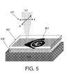
- the execution of motifs (301) may preferably be done by two methods. Either by focal point as shown in Figure 2 , in which the sample will be positioned in a bedplate that is controlled by a system of coordinates (201) and whose positioning control allows obtaining the motifs (301) keeping the laser head (101) fixed.
- Another option is to keep the sample / piece to be marked fixed and being the laser head (101) which moves to define the motifs (301) in question, or by the use of masks (202) as shown in Figure 3 , in which the motifs (301) to be engraved in the material have been previously drawn.
- This mask will be incorporated into the laser optical system (101) and will directly define the motifs (301) without using a positioning system.
- the definition and manufacture of the motifs (301) of the masks may also be manufactured using laser technology (101). This process allows size reduction of the motifs (301) to be manufactured.
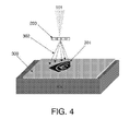
- diffractive masks (203), whose motifs (301) are not identifiable a priori, can be used , these being visually different from those that appear in the mask that is used, as shown in Figure 4 .
- the laser (101) produces the ablation of the layer in areas where it operates, thus leaving an invisible motif that allows the incorporation of adequate information codes and / or pre designed photonic structures.
- the size of the motifs (301) may be macroscopic, microscopic, submicron or even nanometer using a laser (101) of appropriate beam size and scanning.
- the developed structure can subsequently be protected by deposition of a transparent top layer more resistant to abrasion.
- the fluorescent layer (300) deposited on the corresponding substrate (400) is exposed to a laser (101) that moves over its surface as explained in the previous section.
- This laser (101) after being suitably adjusted in depth, allows the internal "writing” of blind motifs (301) that will produce neither absorption nor fluorescence within the rest of the fluorescent layer (300), and also there is no surface ablation of the layer.
- the fluorescent layer (300) can be protected before or after the marking with laser (101) by deposition of another transparent and resistant to abrasion (401) layer.
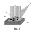
- the fluorescent layer (300) is deposited through a mask (202) where the motifs (301) to be built have been carved.
- the fluorescent motifs (301) originate due to the selective deposition of the fluorescent material in the areas of the substrate (400) not covered by the mask (202), as shown in Figure 6 .
- These fluorescent motifs (301) may be protected by subsequent deposition of a layer made of another material that is transparent and resistant to abrasion,
- the fluorescent layer (300) is exposed to a beam of ultraviolet light (100a), thus eliminating the optical activity of the illuminated areas leading to a structure that would be the negative of the designed by the internal laser marking (101) process, or the selective deposition through masks (202), provided that the mask used was the same.
- the difference is that in this case there is no ablation of the layer material but simply the elimination of its fluorescence and colour in the illuminated areas.
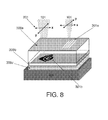
- the versatility of the process object of the invention is such that allows the development of multilayer systems, as shown in Figure 8 , formed by superimposing a series of layers of different fluorescent materials (300a, 300b and 300c), being able to "write" the appropriate motifs (301 a and 301 b) on each of the individual layers using any of the processes described above. Furthermore, the interferometer properties of the multilayer system and the dyes can be exploited to obtain different colours and a visual aspect hardly obtained with other techniques.
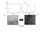
- hydroxyflavone motif by plasma deposition (100) on a glass substrate (400).
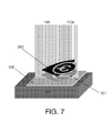
- Obtaining hydroxyflavone polymer layers is performed by the method described in Figure 1 , and the marking of different motifs (301) on them is performed by laser writing as shown in Figure 2 and through the use of masks (202) during the layer deposition process itself, as shown in Figure 7 .
- IF fluorescence intensity
- the second stage describes the process of marking the desired motifs in the fluorescent polymer layer:
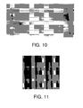
- FIG. 11 shows an image obtained with a fluorescence microscope on a superficial structure where tracks with fluorescent layers and others that don't have it have grown by the process described in Figure 7 .
- motifs (301) or areas that emit light are detected, differentiating them from the motifs (301) or areas where there is not fluorescent material.
- the tracks represented with the lighter colour are the ones containing the fluorescent material as a layer, the other areas correspond to regions of substrate (400) covered by the mask (202) according to the process in Figure 7 and therefore contain no fluorescent material on them.
Landscapes
- Physics & Mathematics (AREA)
- Optics & Photonics (AREA)
- Engineering & Computer Science (AREA)
- Plasma & Fusion (AREA)
- Mechanical Engineering (AREA)
- Thermal Sciences (AREA)
- Manufacturing & Machinery (AREA)
- Credit Cards Or The Like (AREA)
- Thermal Transfer Or Thermal Recording In General (AREA)
- Laser Beam Processing (AREA)
Applications Claiming Priority (2)
| Application Number | Priority Date | Filing Date | Title |
|---|---|---|---|
| ES200900310A ES2343668B1 (es) | 2009-02-04 | 2009-02-04 | Procedimiento de marcaje, encriptacion, etiquetado y codificacion optica. |
| PCT/ES2010/070054 WO2010089439A1 (es) | 2009-02-04 | 2010-02-02 | Procedimiento de marcaje, encriptación, etiquetado y codificación óptica |
Publications (3)
| Publication Number | Publication Date |
|---|---|
| EP2394816A1 true EP2394816A1 (de) | 2011-12-14 |
| EP2394816A4 EP2394816A4 (de) | 2012-07-18 |
| EP2394816B1 EP2394816B1 (de) | 2013-04-17 |
Family
ID=42341726
Family Applications (1)
| Application Number | Title | Priority Date | Filing Date |
|---|---|---|---|
| EP10738235.0A Not-in-force EP2394816B1 (de) | 2009-02-04 | 2010-02-02 | Verfahren für markierung, verschlüsselung, etikettierung und optische kodierung |
Country Status (3)
| Country | Link |
|---|---|
| EP (1) | EP2394816B1 (de) |
| ES (2) | ES2343668B1 (de) |
| WO (1) | WO2010089439A1 (de) |
Cited By (1)
| Publication number | Priority date | Publication date | Assignee | Title |
|---|---|---|---|---|
| EP3109058A3 (de) * | 2015-06-26 | 2017-01-25 | Fraunhofer-Gesellschaft zur Förderung der angewandten Forschung e.V. | Verfahren zur markierung von werkstücken und markiertes werkstück |
Families Citing this family (1)
| Publication number | Priority date | Publication date | Assignee | Title |
|---|---|---|---|---|
| CN114700631B (zh) * | 2022-04-24 | 2022-11-29 | 上海大学 | 钙钛矿-聚合物复合膜的信息加密方法及其应用 |
Family Cites Families (4)
| Publication number | Priority date | Publication date | Assignee | Title |
|---|---|---|---|---|
| US6105501A (en) * | 1998-06-10 | 2000-08-22 | Flex Products, Inc. | High resolution lithographic printing plate suitable for imaging with laser-discharge article and method |
| US6374737B1 (en) * | 2000-03-03 | 2002-04-23 | Alcoa Inc. | Printing plate material with electrocoated layer |
| US7078152B2 (en) * | 2004-05-05 | 2006-07-18 | Presstek, Inc. | Lithographic printing with printing members having plasma polymer layers |
| FI20060177L (fi) * | 2006-02-23 | 2007-08-24 | Picodeon Ltd Oy | Menetelmä tuottaa hyvälaatuisia pintoja ja hyvälaatuisen pinnan omaava tuote |
-
2009
- 2009-02-04 ES ES200900310A patent/ES2343668B1/es not_active Expired - Fee Related
-
2010
- 2010-02-02 EP EP10738235.0A patent/EP2394816B1/de not_active Not-in-force
- 2010-02-02 WO PCT/ES2010/070054 patent/WO2010089439A1/es not_active Ceased
- 2010-02-02 ES ES10738235T patent/ES2415338T3/es active Active
Non-Patent Citations (2)
| Title |
|---|
| No further relevant documents disclosed * |
| See also references of WO2010089439A1 * |
Cited By (1)
| Publication number | Priority date | Publication date | Assignee | Title |
|---|---|---|---|---|
| EP3109058A3 (de) * | 2015-06-26 | 2017-01-25 | Fraunhofer-Gesellschaft zur Förderung der angewandten Forschung e.V. | Verfahren zur markierung von werkstücken und markiertes werkstück |
Also Published As
| Publication number | Publication date |
|---|---|
| WO2010089439A1 (es) | 2010-08-12 |
| ES2343668B1 (es) | 2011-07-22 |
| EP2394816A4 (de) | 2012-07-18 |
| EP2394816B1 (de) | 2013-04-17 |
| ES2343668A1 (es) | 2010-08-05 |
| ES2415338T3 (es) | 2013-07-25 |
Similar Documents
| Publication | Publication Date | Title |
|---|---|---|
| US11951760B2 (en) | Information display medium and manufacturing method relating thereto | |
| TWI753393B (zh) | 用於標記寶石的光學可滲透標記 | |
| EP1321305A2 (de) | Verfahren zur Herstellung von Edelsteinen mit einem einzigartigen mikro-diskreten Zeichen | |
| CN104575263B (zh) | 带鉴别标记的物品、可鉴别标记及方法、观测方法和系统 | |
| He et al. | Review for Micro‐Nano Processing Technology of Microstructures and Metadevices | |
| ATE545518T1 (de) | Datenträger mit mittels laserstrahl eingeschriebenen kennzeichnungen und verfahren zu seiner herstellung | |
| Teutoburg-Weiss et al. | Structural colors with embedded anti-counterfeit features fabricated by laser-based methods | |
| CA2637399A1 (en) | Data storage in a diffractive optical element | |
| EP2394816B1 (de) | Verfahren für markierung, verschlüsselung, etikettierung und optische kodierung | |
| EP3776020B1 (de) | System und verfahren zur ablationsunterstützten nanostrukturbildung für gradientenindexflächen für optiken | |
| JP2002087834A (ja) | エキシマレーザーによる透明部材の加工方法およびその加工品 | |
| KR102441518B1 (ko) | 고종횡비의 초점을 갖는 레이저를 이용하여 기판 상에 미세 패턴을 형성하는 방법 | |
| US9597688B2 (en) | Polymer substrate with fluorescent structure, method for the production thereof and the use thereof | |
| JP2009034691A (ja) | レーザマーキング装置および方法 | |
| CN206075715U (zh) | 一种含有多重衍射图形层的签注透明薄膜及防伪证卡 | |
| Meinertz et al. | Precision marking of glass with excimer lasers: Laser‐generated microstructures and material modifications serve as colored marks | |
| US12330441B2 (en) | Multiple color image | |
| JP2022158738A (ja) | 安全識別のための、整列された散乱体アレイによる光学的デバイス、およびそれを生成する方法 | |
| JP4396345B2 (ja) | パルスレーザーによる材料表面加工方法、情報担体および識別情報 | |
| An et al. | Investigations on color quality improvement through laser-induced surface oxidation for coloration | |
| CN111757813A (zh) | 对固态材料打标的方法、从该方法形成的标记和根据该方法打标的固态材料 | |
| Romanov et al. | PROSPECTS OF" COLORIT" TECHNOLOGY OF COLOR LASER LABELING |
Legal Events
| Date | Code | Title | Description |
|---|---|---|---|
| PUAI | Public reference made under article 153(3) epc to a published international application that has entered the european phase |
Free format text: ORIGINAL CODE: 0009012 |
|
| 17P | Request for examination filed |
Effective date: 20110831 |
|
| AK | Designated contracting states |
Kind code of ref document: A1 Designated state(s): AT BE BG CH CY CZ DE DK EE ES FI FR GB GR HR HU IE IS IT LI LT LU LV MC MK MT NL NO PL PT RO SE SI SK SM TR |
|
| DAX | Request for extension of the european patent (deleted) | ||
| A4 | Supplementary search report drawn up and despatched |
Effective date: 20120615 |
|
| RIC1 | Information provided on ipc code assigned before grant |
Ipc: B41J 3/00 20060101ALI20120611BHEP Ipc: B41M 5/26 20060101ALI20120611BHEP Ipc: B41M 5/24 20060101AFI20120611BHEP Ipc: B41M 3/14 20060101ALI20120611BHEP |
|
| REG | Reference to a national code |
Ref country code: DE Ref legal event code: R079 Ref document number: 602010006430 Country of ref document: DE Free format text: PREVIOUS MAIN CLASS: B41C0001100000 Ipc: B41M0005240000 |
|
| GRAP | Despatch of communication of intention to grant a patent |
Free format text: ORIGINAL CODE: EPIDOSNIGR1 |
|
| RIC1 | Information provided on ipc code assigned before grant |
Ipc: B41M 5/24 20060101AFI20120904BHEP Ipc: B41M 5/26 20060101ALI20120904BHEP Ipc: B41M 3/14 20060101ALI20120904BHEP |
|
| GRAS | Grant fee paid |
Free format text: ORIGINAL CODE: EPIDOSNIGR3 |
|
| GRAA | (expected) grant |
Free format text: ORIGINAL CODE: 0009210 |
|
| AK | Designated contracting states |
Kind code of ref document: B1 Designated state(s): AT BE BG CH CY CZ DE DK EE ES FI FR GB GR HR HU IE IS IT LI LT LU LV MC MK MT NL NO PL PT RO SE SI SK SM TR |
|
| REG | Reference to a national code |
Ref country code: GB Ref legal event code: FG4D |
|
| REG | Reference to a national code |
Ref country code: CH Ref legal event code: EP |
|
| REG | Reference to a national code |
Ref country code: IE Ref legal event code: FG4D |
|
| REG | Reference to a national code |
Ref country code: AT Ref legal event code: REF Ref document number: 607012 Country of ref document: AT Kind code of ref document: T Effective date: 20130515 |
|
| REG | Reference to a national code |
Ref country code: DE Ref legal event code: R096 Ref document number: 602010006430 Country of ref document: DE Effective date: 20130613 |
|
| REG | Reference to a national code |
Ref country code: ES Ref legal event code: FG2A Ref document number: 2415338 Country of ref document: ES Kind code of ref document: T3 Effective date: 20130725 |
|
| REG | Reference to a national code |
Ref country code: AT Ref legal event code: MK05 Ref document number: 607012 Country of ref document: AT Kind code of ref document: T Effective date: 20130417 |
|
| REG | Reference to a national code |
Ref country code: LT Ref legal event code: MG4D |
|
| REG | Reference to a national code |
Ref country code: NL Ref legal event code: VDEP Effective date: 20130417 |
|
| PG25 | Lapsed in a contracting state [announced via postgrant information from national office to epo] |
Ref country code: IS Free format text: LAPSE BECAUSE OF FAILURE TO SUBMIT A TRANSLATION OF THE DESCRIPTION OR TO PAY THE FEE WITHIN THE PRESCRIBED TIME-LIMIT Effective date: 20130817 Ref country code: PT Free format text: LAPSE BECAUSE OF FAILURE TO SUBMIT A TRANSLATION OF THE DESCRIPTION OR TO PAY THE FEE WITHIN THE PRESCRIBED TIME-LIMIT Effective date: 20130819 Ref country code: LT Free format text: LAPSE BECAUSE OF FAILURE TO SUBMIT A TRANSLATION OF THE DESCRIPTION OR TO PAY THE FEE WITHIN THE PRESCRIBED TIME-LIMIT Effective date: 20130417 Ref country code: NO Free format text: LAPSE BECAUSE OF FAILURE TO SUBMIT A TRANSLATION OF THE DESCRIPTION OR TO PAY THE FEE WITHIN THE PRESCRIBED TIME-LIMIT Effective date: 20130717 Ref country code: SI Free format text: LAPSE BECAUSE OF FAILURE TO SUBMIT A TRANSLATION OF THE DESCRIPTION OR TO PAY THE FEE WITHIN THE PRESCRIBED TIME-LIMIT Effective date: 20130417 Ref country code: FI Free format text: LAPSE BECAUSE OF FAILURE TO SUBMIT A TRANSLATION OF THE DESCRIPTION OR TO PAY THE FEE WITHIN THE PRESCRIBED TIME-LIMIT Effective date: 20130417 Ref country code: GR Free format text: LAPSE BECAUSE OF FAILURE TO SUBMIT A TRANSLATION OF THE DESCRIPTION OR TO PAY THE FEE WITHIN THE PRESCRIBED TIME-LIMIT Effective date: 20130718 Ref country code: BE Free format text: LAPSE BECAUSE OF FAILURE TO SUBMIT A TRANSLATION OF THE DESCRIPTION OR TO PAY THE FEE WITHIN THE PRESCRIBED TIME-LIMIT Effective date: 20130417 Ref country code: SE Free format text: LAPSE BECAUSE OF FAILURE TO SUBMIT A TRANSLATION OF THE DESCRIPTION OR TO PAY THE FEE WITHIN THE PRESCRIBED TIME-LIMIT Effective date: 20130417 Ref country code: AT Free format text: LAPSE BECAUSE OF FAILURE TO SUBMIT A TRANSLATION OF THE DESCRIPTION OR TO PAY THE FEE WITHIN THE PRESCRIBED TIME-LIMIT Effective date: 20130417 |
|
| PG25 | Lapsed in a contracting state [announced via postgrant information from national office to epo] |
Ref country code: CY Free format text: LAPSE BECAUSE OF FAILURE TO SUBMIT A TRANSLATION OF THE DESCRIPTION OR TO PAY THE FEE WITHIN THE PRESCRIBED TIME-LIMIT Effective date: 20130417 Ref country code: LV Free format text: LAPSE BECAUSE OF FAILURE TO SUBMIT A TRANSLATION OF THE DESCRIPTION OR TO PAY THE FEE WITHIN THE PRESCRIBED TIME-LIMIT Effective date: 20130417 Ref country code: PL Free format text: LAPSE BECAUSE OF FAILURE TO SUBMIT A TRANSLATION OF THE DESCRIPTION OR TO PAY THE FEE WITHIN THE PRESCRIBED TIME-LIMIT Effective date: 20130417 Ref country code: BG Free format text: LAPSE BECAUSE OF FAILURE TO SUBMIT A TRANSLATION OF THE DESCRIPTION OR TO PAY THE FEE WITHIN THE PRESCRIBED TIME-LIMIT Effective date: 20130717 Ref country code: HR Free format text: LAPSE BECAUSE OF FAILURE TO SUBMIT A TRANSLATION OF THE DESCRIPTION OR TO PAY THE FEE WITHIN THE PRESCRIBED TIME-LIMIT Effective date: 20130417 |
|
| PG25 | Lapsed in a contracting state [announced via postgrant information from national office to epo] |
Ref country code: CZ Free format text: LAPSE BECAUSE OF FAILURE TO SUBMIT A TRANSLATION OF THE DESCRIPTION OR TO PAY THE FEE WITHIN THE PRESCRIBED TIME-LIMIT Effective date: 20130417 Ref country code: SK Free format text: LAPSE BECAUSE OF FAILURE TO SUBMIT A TRANSLATION OF THE DESCRIPTION OR TO PAY THE FEE WITHIN THE PRESCRIBED TIME-LIMIT Effective date: 20130417 Ref country code: EE Free format text: LAPSE BECAUSE OF FAILURE TO SUBMIT A TRANSLATION OF THE DESCRIPTION OR TO PAY THE FEE WITHIN THE PRESCRIBED TIME-LIMIT Effective date: 20130417 Ref country code: DK Free format text: LAPSE BECAUSE OF FAILURE TO SUBMIT A TRANSLATION OF THE DESCRIPTION OR TO PAY THE FEE WITHIN THE PRESCRIBED TIME-LIMIT Effective date: 20130417 |
|
| PLBE | No opposition filed within time limit |
Free format text: ORIGINAL CODE: 0009261 |
|
| STAA | Information on the status of an ep patent application or granted ep patent |
Free format text: STATUS: NO OPPOSITION FILED WITHIN TIME LIMIT |
|
| PG25 | Lapsed in a contracting state [announced via postgrant information from national office to epo] |
Ref country code: NL Free format text: LAPSE BECAUSE OF FAILURE TO SUBMIT A TRANSLATION OF THE DESCRIPTION OR TO PAY THE FEE WITHIN THE PRESCRIBED TIME-LIMIT Effective date: 20130417 Ref country code: RO Free format text: LAPSE BECAUSE OF FAILURE TO SUBMIT A TRANSLATION OF THE DESCRIPTION OR TO PAY THE FEE WITHIN THE PRESCRIBED TIME-LIMIT Effective date: 20130417 Ref country code: IT Free format text: LAPSE BECAUSE OF FAILURE TO SUBMIT A TRANSLATION OF THE DESCRIPTION OR TO PAY THE FEE WITHIN THE PRESCRIBED TIME-LIMIT Effective date: 20130417 |
|
| 26N | No opposition filed |
Effective date: 20140120 |
|
| REG | Reference to a national code |
Ref country code: DE Ref legal event code: R097 Ref document number: 602010006430 Country of ref document: DE Effective date: 20140120 |
|
| PG25 | Lapsed in a contracting state [announced via postgrant information from national office to epo] |
Ref country code: LU Free format text: LAPSE BECAUSE OF FAILURE TO SUBMIT A TRANSLATION OF THE DESCRIPTION OR TO PAY THE FEE WITHIN THE PRESCRIBED TIME-LIMIT Effective date: 20140202 Ref country code: MC Free format text: LAPSE BECAUSE OF FAILURE TO SUBMIT A TRANSLATION OF THE DESCRIPTION OR TO PAY THE FEE WITHIN THE PRESCRIBED TIME-LIMIT Effective date: 20130417 |
|
| REG | Reference to a national code |
Ref country code: CH Ref legal event code: PL |
|
| PG25 | Lapsed in a contracting state [announced via postgrant information from national office to epo] |
Ref country code: LI Free format text: LAPSE BECAUSE OF NON-PAYMENT OF DUE FEES Effective date: 20140228 Ref country code: CH Free format text: LAPSE BECAUSE OF NON-PAYMENT OF DUE FEES Effective date: 20140228 |
|
| REG | Reference to a national code |
Ref country code: IE Ref legal event code: MM4A |
|
| PG25 | Lapsed in a contracting state [announced via postgrant information from national office to epo] |
Ref country code: IE Free format text: LAPSE BECAUSE OF NON-PAYMENT OF DUE FEES Effective date: 20140202 |
|
| REG | Reference to a national code |
Ref country code: FR Ref legal event code: PLFP Year of fee payment: 6 |
|
| REG | Reference to a national code |
Ref country code: FR Ref legal event code: PLFP Year of fee payment: 7 |
|
| PG25 | Lapsed in a contracting state [announced via postgrant information from national office to epo] |
Ref country code: MT Free format text: LAPSE BECAUSE OF FAILURE TO SUBMIT A TRANSLATION OF THE DESCRIPTION OR TO PAY THE FEE WITHIN THE PRESCRIBED TIME-LIMIT Effective date: 20130417 |
|
| PG25 | Lapsed in a contracting state [announced via postgrant information from national office to epo] |
Ref country code: SM Free format text: LAPSE BECAUSE OF FAILURE TO SUBMIT A TRANSLATION OF THE DESCRIPTION OR TO PAY THE FEE WITHIN THE PRESCRIBED TIME-LIMIT Effective date: 20130417 |
|
| PGFP | Annual fee paid to national office [announced via postgrant information from national office to epo] |
Ref country code: DE Payment date: 20160226 Year of fee payment: 7 |
|
| PGFP | Annual fee paid to national office [announced via postgrant information from national office to epo] |
Ref country code: FR Payment date: 20160217 Year of fee payment: 7 Ref country code: GB Payment date: 20160226 Year of fee payment: 7 |
|
| PG25 | Lapsed in a contracting state [announced via postgrant information from national office to epo] |
Ref country code: HU Free format text: LAPSE BECAUSE OF FAILURE TO SUBMIT A TRANSLATION OF THE DESCRIPTION OR TO PAY THE FEE WITHIN THE PRESCRIBED TIME-LIMIT; INVALID AB INITIO Effective date: 20100202 Ref country code: TR Free format text: LAPSE BECAUSE OF FAILURE TO SUBMIT A TRANSLATION OF THE DESCRIPTION OR TO PAY THE FEE WITHIN THE PRESCRIBED TIME-LIMIT Effective date: 20130417 |
|
| REG | Reference to a national code |
Ref country code: DE Ref legal event code: R119 Ref document number: 602010006430 Country of ref document: DE |
|
| GBPC | Gb: european patent ceased through non-payment of renewal fee |
Effective date: 20170202 |
|
| REG | Reference to a national code |
Ref country code: FR Ref legal event code: ST Effective date: 20171031 |
|
| PG25 | Lapsed in a contracting state [announced via postgrant information from national office to epo] |
Ref country code: FR Free format text: LAPSE BECAUSE OF NON-PAYMENT OF DUE FEES Effective date: 20170228 Ref country code: DE Free format text: LAPSE BECAUSE OF NON-PAYMENT OF DUE FEES Effective date: 20170901 |
|
| PG25 | Lapsed in a contracting state [announced via postgrant information from national office to epo] |
Ref country code: GB Free format text: LAPSE BECAUSE OF NON-PAYMENT OF DUE FEES Effective date: 20170202 |
|
| PG25 | Lapsed in a contracting state [announced via postgrant information from national office to epo] |
Ref country code: MK Free format text: LAPSE BECAUSE OF FAILURE TO SUBMIT A TRANSLATION OF THE DESCRIPTION OR TO PAY THE FEE WITHIN THE PRESCRIBED TIME-LIMIT Effective date: 20130417 |
|
| REG | Reference to a national code |
Ref country code: ES Ref legal event code: FD2A Effective date: 20180704 |
|
| PG25 | Lapsed in a contracting state [announced via postgrant information from national office to epo] |
Ref country code: ES Free format text: LAPSE BECAUSE OF NON-PAYMENT OF DUE FEES Effective date: 20170203 |
|
| REG | Reference to a national code |
Ref country code: ES Ref legal event code: NE2A Effective date: 20190115 |
|
| PG25 | Lapsed in a contracting state [announced via postgrant information from national office to epo] |
Ref country code: ES Free format text: LAPSE BECAUSE OF NON-PAYMENT OF DUE FEES Effective date: 20170203 |
|
| PGFP | Annual fee paid to national office [announced via postgrant information from national office to epo] |
Ref country code: ES Payment date: 20190306 Year of fee payment: 10 |
|
| PGRI | Patent reinstated in contracting state [announced from national office to epo] |
Ref country code: ES Effective date: 20190115 |
|
| REG | Reference to a national code |
Ref country code: ES Ref legal event code: FD2A Effective date: 20230619 |
|
| PG25 | Lapsed in a contracting state [announced via postgrant information from national office to epo] |
Ref country code: ES Free format text: THE PATENT HAS BEEN ANNULLED BY A DECISION OF A NATIONAL AUTHORITY Effective date: 20200203 |