EP2394499B1 - Elektrooptisches steuer- oder regelgerät zum austausch von steuer- oder regelsignalen - Google Patents
Elektrooptisches steuer- oder regelgerät zum austausch von steuer- oder regelsignalen Download PDFInfo
- Publication number
- EP2394499B1 EP2394499B1 EP10701682.6A EP10701682A EP2394499B1 EP 2394499 B1 EP2394499 B1 EP 2394499B1 EP 10701682 A EP10701682 A EP 10701682A EP 2394499 B1 EP2394499 B1 EP 2394499B1
- Authority
- EP
- European Patent Office
- Prior art keywords
- optical
- circuit board
- control
- reinforced layer
- fibre reinforced
- Prior art date
- Legal status (The legal status is an assumption and is not a legal conclusion. Google has not performed a legal analysis and makes no representation as to the accuracy of the status listed.)
- Not-in-force
Links
Images


Classifications
-
- G—PHYSICS
- G02—OPTICS
- G02B—OPTICAL ELEMENTS, SYSTEMS OR APPARATUS
- G02B6/00—Light guides; Structural details of arrangements comprising light guides and other optical elements, e.g. couplings
- G02B6/24—Coupling light guides
- G02B6/42—Coupling light guides with opto-electronic elements
- G02B6/43—Arrangements comprising a plurality of opto-electronic elements and associated optical interconnections
-
- G—PHYSICS
- G02—OPTICS
- G02B—OPTICAL ELEMENTS, SYSTEMS OR APPARATUS
- G02B6/00—Light guides; Structural details of arrangements comprising light guides and other optical elements, e.g. couplings
- G02B6/24—Coupling light guides
- G02B6/42—Coupling light guides with opto-electronic elements
- G02B6/4201—Packages, e.g. shape, construction, internal or external details
-
- H—ELECTRICITY
- H05—ELECTRIC TECHNIQUES NOT OTHERWISE PROVIDED FOR
- H05K—PRINTED CIRCUITS; CASINGS OR CONSTRUCTIONAL DETAILS OF ELECTRIC APPARATUS; MANUFACTURE OF ASSEMBLAGES OF ELECTRICAL COMPONENTS
- H05K1/00—Printed circuits
- H05K1/02—Details
- H05K1/0274—Optical details, e.g. printed circuits comprising integral optical means
-
- H—ELECTRICITY
- H05—ELECTRIC TECHNIQUES NOT OTHERWISE PROVIDED FOR
- H05K—PRINTED CIRCUITS; CASINGS OR CONSTRUCTIONAL DETAILS OF ELECTRIC APPARATUS; MANUFACTURE OF ASSEMBLAGES OF ELECTRICAL COMPONENTS
- H05K1/00—Printed circuits
- H05K1/02—Details
- H05K1/03—Use of materials for the substrate
- H05K1/0313—Organic insulating material
- H05K1/0353—Organic insulating material consisting of two or more materials, e.g. two or more polymers, polymer + filler, + reinforcement
- H05K1/0366—Organic insulating material consisting of two or more materials, e.g. two or more polymers, polymer + filler, + reinforcement reinforced, e.g. by fibres, fabrics
-
- H—ELECTRICITY
- H05—ELECTRIC TECHNIQUES NOT OTHERWISE PROVIDED FOR
- H05K—PRINTED CIRCUITS; CASINGS OR CONSTRUCTIONAL DETAILS OF ELECTRIC APPARATUS; MANUFACTURE OF ASSEMBLAGES OF ELECTRICAL COMPONENTS
- H05K2201/00—Indexing scheme relating to printed circuits covered by H05K1/00
- H05K2201/02—Fillers; Particles; Fibers; Reinforcement materials
- H05K2201/0275—Fibers and reinforcement materials
- H05K2201/029—Woven fibrous reinforcement or textile
-
- H—ELECTRICITY
- H05—ELECTRIC TECHNIQUES NOT OTHERWISE PROVIDED FOR
- H05K—PRINTED CIRCUITS; CASINGS OR CONSTRUCTIONAL DETAILS OF ELECTRIC APPARATUS; MANUFACTURE OF ASSEMBLAGES OF ELECTRICAL COMPONENTS
- H05K2201/00—Indexing scheme relating to printed circuits covered by H05K1/00
- H05K2201/09—Shape and layout
- H05K2201/09209—Shape and layout details of conductors
- H05K2201/09654—Shape and layout details of conductors covering at least two types of conductors provided for in H05K2201/09218 - H05K2201/095
- H05K2201/0969—Apertured conductors
-
- H—ELECTRICITY
- H05—ELECTRIC TECHNIQUES NOT OTHERWISE PROVIDED FOR
- H05K—PRINTED CIRCUITS; CASINGS OR CONSTRUCTIONAL DETAILS OF ELECTRIC APPARATUS; MANUFACTURE OF ASSEMBLAGES OF ELECTRICAL COMPONENTS
- H05K2201/00—Indexing scheme relating to printed circuits covered by H05K1/00
- H05K2201/10—Details of components or other objects attached to or integrated in a printed circuit board
- H05K2201/10431—Details of mounted components
- H05K2201/10507—Involving several components
- H05K2201/10545—Related components mounted on both sides of the PCB
-
- H—ELECTRICITY
- H05—ELECTRIC TECHNIQUES NOT OTHERWISE PROVIDED FOR
- H05K—PRINTED CIRCUITS; CASINGS OR CONSTRUCTIONAL DETAILS OF ELECTRIC APPARATUS; MANUFACTURE OF ASSEMBLAGES OF ELECTRICAL COMPONENTS
- H05K2201/00—Indexing scheme relating to printed circuits covered by H05K1/00
- H05K2201/20—Details of printed circuits not provided for in H05K2201/01 - H05K2201/10
- H05K2201/2054—Light-reflecting surface, e.g. conductors, substrates, coatings, dielectrics
Definitions
- the invention relates to an electro-optical control or regulating device.
- the control or regulating device has a central control unit, which is arranged on at least one circuit board with a glass fiber reinforcement.
- a printed circuit board and a manufacture thereof is from the document DE 10 2004 014 221 A1
- the switch card or circuit board has copper cladding on both sides of a semi-cured prepreg.
- optical fibers are contained in the printed circuit board, which are arranged at regular intervals by fixing tools in the printed switch card and embedded in an epoxy resin.
- the periodically-spaced optical fibers serve to transmit an optical signal, and the copper claddings may be patterned.
- circuit board has the disadvantage that a considerable effort is required to incorporate in the circuit board optical transmission means at specified intervals and lengths. This is costly and limits the possibilities of optical transmission to the introduced into the circuit boards optical fibers.
- the US 2007/0154132 A1 teaches one skilled in the art an electro-optic control or regulating device and method for exchanging control or regulating signals.
- the control or regulating device has a central control unit, which is arranged on at least one circuit board with a glass fiber reinforcement is. Data of the control unit is optically transmitted to a radiation source and via an optical transmission means to a detector, wherein the glass fiber reinforcement is provided as an optical transmission means.
- This transmission principle is also applicable to multilayer printed circuit boards having a plurality of patterned metal layers within the printed circuit board as long as glass fiber fabric structures are provided for reinforcement in the multilayer printed circuit board. These fibers are then used not only for amplification but also for the optical transmission of signals. These optical transmission paths through the circuit board have the advantage that interference-proof transmission channels for high transmission rates compared to printed circuit structures of a structured Kupferkaschtechnik can be created, and thus a trouble-free transmission solution for sensitive amounts of data is available.
- a printed circuit board with optical position according to the US 2005/0063637 A1 of the WO 2005/078497 A1 or the WO 2007/114384 A1 is at least one glass fiber reinforcement layer in a horizontal plane parallel to the top or to the back of the circuit board and transmits signals between the radiation source and the detector.
- the GB 1 385 526 discloses a circuit board in which a glass fiber reinforcement layer comprises a glass fiber fabric in which optical signal data is transferable in all horizontal directions and the fabric intersections form optical coupling nodes.
- the US 2006/0093259 A1 and the EP 0 986 197 A2 disclose optical transmissions in a printed circuit board in which an optical radiation source and an optical detector are arranged in corresponding recesses of the board such that their optical axes are arranged in a plane of a glass fiber reinforcement layer and aligned with each other.
- the object of the invention is to provide additional transmission paths in a circuit board, which supplement the metallic circuit structures of a printed circuit board without having to make costly installations in the circuit board.
- an electro-optical control or regulating device has a control unit which is arranged on at least one circuit board which has an upper glass fiber reinforcement layer and a lower glass fiber reinforcement layer.
- Data of the control unit is optically transmitted from a radiation source via the upper glass fiber reinforcement layer and the lower glass fiber reinforcement layer as an optical transmission means to a detector, wherein a recess in the circuit board has a one-sided metallic coating, which over the upper Glass fiber amplification layer reflected radiation of the radiation source reflected, and arranged on the underside of the circuit board recess having an optical detector, wherein the reflected beam is fed into the deeper glass fiber reinforcement layer of the circuit board and is received by the detector.
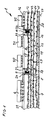
- FIG. 1 shows a schematic cross section through an electro-optical control and / or regulating device 1.
- the control and / or regulating device 1 at least one control unit 6, which is connected via a metallic circuit structure 29 on the upper side 16 of a circuit board 7 with a radiation source 9 , wherein this optical radiation source 9 is arranged in a recess 21 of the circuit board 7.
- the circuit board 7 has a plurality of glass fiber reinforcing layers 12 to 15, which are formed as a glass fiber fabric 18, so that glass fibers in the horizontal direction extend both along the cross section shown here and orthogonal to the plane of the drawing.
- optical coupling nodes 19 result in the tissue.
- the recess 21 is incorporated so deeply into the circuit board 7 that the radiation source 9 via the glass fiber reinforcement layer 12 forms an optical connection with a detector 11 which is arranged in a further recess 22.
- Another advantage is that without additional effort now the glass fiber reinforcement layers 12 to 15 are used for signal transmission, while above the glass fiber reinforcement layers 12 to 15 on top 16 of the circuit board 7 more semiconductor devices 30 and 31 via the circuit structure 29 with the control unit 6 cooperate can.
- the detector 11 in the recess 22 can also interact with a further semiconductor component 32 via the circuit structure 29 via a metallic coating 24 in the recess 22, which is connected to the circuit structure 29.
- the inventive use of the glass fiber fabric 18 opens up an improvement in the complexity of electro-optical control or regulating devices.
- FIG. 2 shows a schematic cross section through an optical transmission path 40 according to FIG. 1 , From the in FIG. 1 shown fiberglass reinforcing layers 12 to 15 is shown in FIG 2, only the gain layer 12 between the optical radiation source 9 and the optical detector 11 is shown. In this case, the optical radiation source 9 and the optical detector 11 are aligned with their optical axes 20 to each other, wherein the common optical axis 20 is arranged in the region of the horizontal glass fiber layer 12.
- the recesses 21 and 22 can be realized by simple Einfräsungen in the circuit board. Both the optical radiation source 9 and the optical detector 11 may be provided with a lens system 33 and a solder connection 36 to the circuit structure 29 on its front side 34, while their backs 17 with a metallic back electrode 37 on a metallic coating 24 of the recess 21 and 22 are fixed. The metallic coatings 24 of the recesses 21 and 22 are in electrical contact with the circuit structure 29 on the upper surface 16 of the electro-optical control apparatus.
- FIG. 3 shows a schematic cross section through an optical transmission path 40 in a circuit board 7 according to the invention an electro-optical control or regulating device 2.
- a radiation reflector is provided in a recess 23 which of the metallic coating 24th is formed.
- the transmitted via an upper glass fiber reinforcing layer 12 light signals are reflected at the metallic coating 24 in the recess 23, wherein the reflected beam 25 is fed into a deeper glass fiber reinforcing layer 14 of the circuit board 7 and arranged in a arranged on the bottom 17 of the circuit board 7 recess 22 of a optical detector 11 is received and the metal layer 28 on the underside of the circuit board 17 is supplied.
- this optical transmission path 40 it is possible to connect semiconductor components on the upper side 16 with semiconductor components on the underside 17 via the optical transmission path 40.
Landscapes
- Physics & Mathematics (AREA)
- General Physics & Mathematics (AREA)
- Optics & Photonics (AREA)
- Engineering & Computer Science (AREA)
- Microelectronics & Electronic Packaging (AREA)
- Optical Couplings Of Light Guides (AREA)
Description
- Die Erfindung betrifft ein elektrooptisches Steuer- oder Regelgerät. Dazu weist das Steuer- oder Regelgerät eine zentrale Steuereinheit auf, die auf mindestens einer Schaltungsplatine mit einer Glasfaserverstärkung angeordnet ist.
- Eine gedruckte Schalterkarte und eine Herstellung derselben ist aus der Druckschrift
DE 10 2004 014 221 A1 bekannt, wobei die Schalterkarte oder Schaltungsplatine Kupferplattierungen auf beiden Seiten eines halbgehärteten Prepregs aufweist. Dabei sind in der gedruckten Schaltungsplatine optische Fasern enthalten, die mit regelmäßigen Zwischenräumen durch Fixierwerkzeuge in der gedruckten Schalterkarte angeordnet und in einem Epoxidharz eingebettet sind. Die mit regelmäßigen Zwischenräumen eingebetteten optischen Fasern dienen der Übertragung eines optischen Signals, wobei die Kupferplattierungen strukturiert sein können. - Eine derartige Schaltkarte hat den Nachteil, dass ein erheblicher Aufwand erforderlich ist, um in die Schaltungsplatine optische Übertragungsmittel in festgelegten Abständen und Längen einzubauen. Dieses ist kostenintensiv und schränkt die Möglichkeiten der optischen Übertragung auf die in die Schaltungsplatinen eingebrachten Lichtleitfasern ein.
- Die
US 2007/0154132 A1 lehrt den Fachmann ein elektrooptisches Steuer- oder Regelgerät und ein Verfahren zum Austausch von Steuer- oder Regelsignalen. Das Steuer- oder Regelgerät weist eine zentrale Steuereinheit auf, die auf mindestens einer Schaltungsplatine mit einer Glasfaserverstärkung angeordnet ist. Daten der Steuereinheit werden optisch an eine Strahlungsquelle und über ein optisches Übertragungsmittel zu einem Detektor übertragen, wobei als optisches Übertragungsmittel die Glasfaserverstärkung vorgesehen ist. - Durch dieses elektrooptische Steuer- oder Regelgerät können neue zusätzliche Übertragungswege in einer Leiterplatte, die unterhalb der Bestückungsseite einer Leiterplatine durch die Glasfaserverstärkung in faserverstärkten Schaltungsplatinen vorhanden sind, zusätzlich zu den metallischen Strukturen genutzt werden. Diese Übermittlungswege können ohne zusätzlichen Kostenaufwand betrieben werden, während oberhalb dieser Übermittlungswege eine Mehrzahlzahl von Bauelementen zusätzlich zu der Steuereinheit des elektrooptischen Steuer- oder Regelgerätes positioniert sein können.
- Dieses Übertragungsprinzip ist auch für mehrschichtige Leiterplatten mit einer Mehrzahl von strukturierten Metallschichten innerhalb der Leiterplatte anwendbar, solange Glasfasergewebestrukturen zur Verstärkung in der mehrschichtigen Leiterplatte vorgesehen sind. Diese Glasfasern werden dann nicht nur zur Verstärkung, sondern auch zur optischen Übertragung von Signalen genutzt. Diese optischen Übertragungswege durch die Schaltungsplatine haben den Vorteil, dass störungssichere Übertragungskanäle für hohe Übertragungsraten im Vergleich zu Leiterbahnstrukturen einer strukturierten Kupferkaschierung geschaffen werden können, und somit eine störungssichere Übertragungslösung für sensible Datenmengen zur Verfügung steht.
- Bei einer Leiterplatte mit optischer Lage gemäß der
US 2005/0063637 A1 , derWO 2005/078497 A1 oder derWO 2007/114384 A1 ist mindestens eine Glasfaserverstärkungslage in einer horizontalen Ebene parallel zu der Oberseite oder zu der Rückseite der Schaltungsplatine angeordnet und überträgt Signale zwischen der Strahlungsquelle und dem Detektor. - Die
GB 1 385 526 - Die
US 2006/0093259 A1 und dieEP 0 986 197 A2 offenbaren optische Übertragungen in einer Leiterplatte bei denen eine optische Strahlungsquelle und ein optischer Detektors in entsprechenden Aussparungen der Platine derart angeordnet, dass ihre optischen Achsen in einer Ebene einer Glasfaserverstärkungslage angeordnet und aufeinander ausgerichtet sind sind. - Aufgabe der Erfindung ist es, in einer Schaltungsplatine zusätzliche Übertragungswege zu schaffen, welche die metallischen Schaltungsstrukturen einer gedruckten Leiterplatte ergänzen, ohne kostenintensive Einbauten in die Schaltungsplatine vornehmen zu müssen.
- Diese Aufgabe wird mit dem Gegenstand des unabhängigen Anspruchs gelöst. Vorteilhafte Weiterbildungen der Erfindung ergeben sich aus dem abhängigen Anspruch.
- In erfindungsgemäßer Weise weist ein elektrooptisches Steuer- oder Regelgerät eine Steuereinheit auf, die auf mindestens einer Schaltungsplatine, die eine obere Glasfaserverstärkungslage und eine tiefere Glasfaserverstärkungslage aufweist, angeordnet ist. Daten der Steuereinheit werden optisch von einer Strahlungsquelle über die obere Glasfaserverstärkungslage und die tiefere Glasfaserverstärkungslage als optischem Übertragungsmittel zu einem Detektor übertragen, wobei eine Aussparung in der Schaltungsplatine eine einseitige metallische Beschichtung aufweist, welche die über die obere Glasfaserverstärkungslage übertragene Strahlung der Strahlungsquelle reflektiert, und eine auf der Unterseite der Schaltungsplatine angeordnete Aussparung einen optischen Detektor aufweist, wobei der reflektierte Strahl in die tiefere Glasfaserverstärkungslage der Schaltungsplatine eingespeist wird und von dem Detektor empfangen wird.
- Die Erfindung wird nun anhand der beigefügten Figuren näher erläutert.
- Figur 1
- zeigt einen schematischen Querschnitt durch ein elektrooptisches Steuer- und/oder Regelgerät einer ersten Ausführungsform gemäß dem Stand der Technik;
- Figur 2
- zeigt einen schematischen Querschnitt durch eine optische Übertragungsstrecke gemäß
Figur 1 ; - Figur 3
- zeigt einen schematischen Querschnitt durch eine optische Übertragungsstrecke in einer Schaltungsplatine gemäß der Erfindung;
-
Figur 1 zeigt einen schematischen Querschnitt durch ein elektrooptisches Steuer- und/oder Regelungsgerät 1. Dazu weist das Steuer- und/oder Regelungsgerät 1 mindestens eine Steuereinheit 6 auf, die über eine metallische Schaltungsstruktur 29 auf der Oberseite 16 einer Schaltungsplatine 7 mit einer Strahlungsquelle 9 verbunden ist, wobei diese optischen Strahlungsquelle 9 in einer Aussparung 21 der Schaltungsplatine 7 angeordnet ist. - Die Schaltungsplatine 7 weist eine Mehrzahl von Glasfaserverstärkungslagen 12 bis 15 auf, die als Glasfasergewebe 18 ausgebildet sind, so dass sich Glasfasern in horizontaler Richtung sowohl entlang des hier gezeigten Querschnitts als auch orthogonal zu der Zeichenebene erstrecken. Dabei ergeben sich zusätzlich optische Koppelknoten 19 in dem Gewebe.
- Die Aussparung 21 ist derart tief in die Leiterplatte 7 eingearbeitet, dass die Strahlungsquelle 9 über die Glasfaserverstärkungslage 12 eine optische Verbindung mit einem Detektor 11, der in einer weiteren Aussparung 22 angeordnet ist, bildet. Mit einer derartigen optischen Übertragungsstrecke 40 über das Übertragungsmittel 10 in Form einer Glasfaserverstärkung 8 der Schaltungsplatine 7 wird ein weiterer zusätzlicher Verbindungsweg zu den vorhandenen metallischen Verbindungen auf der Oberseite 16 der Schaltungsplatine 7 oder auf Zwischenmetalllagen einer mehrschichtigen Schaltungsplatine 7 geschaffen.
- Ein weiterer Vorteil besteht darin, dass ohne zusätzlichen großen Aufwand nun die Glasfaserverstärkungslagen 12 bis 15 zur Signalübermittlung genutzt werden, während oberhalb der Glasfaserverstärkungslagen 12 bis 15 auf der Oberseite 16 der Schaltungsplatine 7 weitere Halbleiterbauelemente 30 und 31 über die Schaltungsstruktur 29 mit der Steuereinheit 6 zusammenwirken können. Auch der Detektor 11 in der Aussparung 22 kann über eine metallische Beschichtung 24 in der Aussparung 22, die mit der Schaltungsstruktur 29 in Verbindung steht, mit einem weiteren Halbleiterbauelement 32 über die Schaltungsstruktur 29 zusammenwirken. Somit eröffnet die erfindungsgemäße Nutzung des Glasfasergewebes 18 eine Verbesserung der Komplexität von elektrooptischen Steuer- oder Regelgeräten.
-
Figur 2 zeigt einen schematischen Querschnitt durch eine optische Übertragungsstrecke 40 gemäßFigur 1 . Von den inFigur 1 gezeigten Glasfaserverstärkungslagen 12 bis 15 wird in Figur 2 lediglich die Verstärkungslage 12 zwischen der optischen Strahlungsquelle 9 und dem optischen Detektor 11 gezeigt. Dabei sind die optische Strahlungsquelle 9 und der optische Detektor 11 mit ihren optischen Achsen 20 aufeinander ausgerichtet, wobei die gemeinsame optische Achse 20 im Bereich der horizontalen Glasfaserlage 12 angeordnet ist. - Die Aussparungen 21 und 22 können durch einfache Einfräsungen in die Leiterplatte realisiert werden. Sowohl die optische Strahlungsquelle 9 als auch der optische Detektor 11 können mit einem Linsensystem 33 und einer Lötverbindung 36 zu der Schaltungsstruktur 29 auf ihrer Frontseite 34 ausgestattet sein, während ihre Rückseiten 17 mit einer metallischen Rückseitenelektrode 37 auf einer metallischen Beschichtung 24 der Aussparung 21 bzw. 22 fixiert sind. Die metallischen Beschichtungen 24 der Aussparungen 21 und 22 stehen mit der Schaltungsstruktur 29 auf der Oberseite 16 des elektrooptischen Steuer- oder Regelgeräts elektrisch in Kontakt.
-
Figur 3 zeigt einen schematischen Querschnitt durch eine optische Übertragungsstrecke 40 in einer Schaltungsplatine 7 gemäß eines erfindungsgemäßen elektrooptischen Steuer- oder Regelgeräts 2. In dieser Übertragungsstrecke 40 ist zwischen der Strahlungsquelle 9 und dem Detektor 11 ein Strahlungsreflektor in einer Aussparung 23 vorgesehen, der von der metallischen Beschichtung 24 gebildet wird. Die über eine obere Glasfaserverstärkungslage 12 übertragenen Lichtsignale werden an der metallischen Beschichtung 24 in der Aussparung 23 reflektiert, wobei der reflektierte Strahl 25 in eine tiefere Glasfaserverstärkungslage 14 der Schaltungsplatine 7 eingespeist wird und in einer auf der Unterseite 17 der Schaltungsplatine 7 angeordneten Aussparung 22 von einem optischen Detektor 11 empfangen und der Metallschicht 28 auf der Unterseite der Schaltungsplatine 17 zugeführt wird. Somit ist es mit dieser optischen Übertragungsstrecke 40 möglich, Halbleiterbauelemente auf der Oberseite 16 mit Halbleiterbauelementen auf der Unterseite 17 über die optische Übertragungsstrecke 40 miteinander zu verbinden.
Claims (2)
- Elektrooptisches Steuer- oder Regelgerät (1) mit einer Steuereinheit (6) wobei:- die Steuereinheit (6) auf mindestens einer Schaltungsplatine (7), die eine obere Glasfaserverstärkungslage (12) und eine tiefere Glasfaserverstärkungslage (14) aufweist, angeordnet ist, und- Daten der Steuereinheit (6) optisch von einer Strahlungsquelle (9) über die obere Glasfaserverstärkungslage (12) und die tiefere Glasfaserverstärkungslage (14) als optischem Übertragungsmittel (10) zu einem Detektor (11) übertragen werden,dadurch gekennzeichnet, dass
eine Aussparung (23) in der Schaltungsplatine (7) eine einseitige metallische Beschichtung (24) aufweist, welche die über die obere Glasfaserverstärkungslage (12) übertragene Strahlung der Strahlungsquelle (9) reflektiert, und
eine auf der Unterseite (17) der Schaltungsplatine (7) angeordnete Aussparung (22) einen optischen Detektor (11) aufweist,
wobei der reflektierte Strahl (25) in die tiefere Glasfaserverstärkungslage (14) der Schaltungsplatine (7) eingespeist wird und von dem Detektor (11) empfangen wird. - Steuer- oder Regelgerät nach Anspruch 1,
dadurch gekennzeichnet, dass die mindestens eine Glasfaserverstärkungslage (12 bis 15) ein Glasfasergewebe (18) aufweist, in dem optische Signaldaten in alle horizontalen Richtungen übertragbar sind und die Gewebekreuzungen optisch Koppelknoten bilden.
Applications Claiming Priority (2)
| Application Number | Priority Date | Filing Date | Title |
|---|---|---|---|
| DE200910008087 DE102009008087A1 (de) | 2009-02-09 | 2009-02-09 | Elektrooptisches Steuer-oder Regelgerät und Verfahren zum Austausch von Steuer-und Regelsignalen |
| PCT/EP2010/051068 WO2010089254A1 (de) | 2009-02-09 | 2010-01-29 | Elektrooptisches steuer- oder regelgerät und verfahren zum austausch von steuer- oder regelsignalen |
Publications (2)
| Publication Number | Publication Date |
|---|---|
| EP2394499A1 EP2394499A1 (de) | 2011-12-14 |
| EP2394499B1 true EP2394499B1 (de) | 2013-05-29 |
Family
ID=41698033
Family Applications (1)
| Application Number | Title | Priority Date | Filing Date |
|---|---|---|---|
| EP10701682.6A Not-in-force EP2394499B1 (de) | 2009-02-09 | 2010-01-29 | Elektrooptisches steuer- oder regelgerät zum austausch von steuer- oder regelsignalen |
Country Status (3)
| Country | Link |
|---|---|
| EP (1) | EP2394499B1 (de) |
| DE (1) | DE102009008087A1 (de) |
| WO (1) | WO2010089254A1 (de) |
Families Citing this family (4)
| Publication number | Priority date | Publication date | Assignee | Title |
|---|---|---|---|---|
| DE102012218570A1 (de) * | 2012-10-11 | 2014-04-17 | Osram Gmbh | Elektronisches vorschaltgerät für eine strahlungseinheit |
| US9175993B2 (en) | 2013-09-26 | 2015-11-03 | Rosemount Inc. | Industrial process field device with low power optical isolator |
| US9228869B2 (en) | 2013-09-26 | 2016-01-05 | Rosemount Inc. | Industrial process variable transmitter with isolated power scavenging intrinsically safe pulse output circuitry |
| US10075246B2 (en) | 2013-09-26 | 2018-09-11 | Micro Motion, Inc. | Optical isolator mounted in printed circuit board recess |
Family Cites Families (12)
| Publication number | Priority date | Publication date | Assignee | Title |
|---|---|---|---|---|
| DE2120768A1 (de) | 1971-04-28 | 1972-11-16 | Siemens AG, 1000 Berlin u. 8000 München | Glasfaserverstärkte Konstruktionselemente, Leiterplatten oder dergleichen |
| DE2343235B2 (de) * | 1973-08-28 | 1978-09-28 | Philips Patentverwaltung Gmbh, 2000 Hamburg | Verfahren zur Befestigung und Kontaktierung von elektrischen Subminiatur-Bauelementen auf gedruckten Schaltungen |
| DE19643911A1 (de) * | 1996-10-30 | 1998-05-07 | Sick Ag | Schaltungsanordnung mit auf einem mit Leiterbahnen versehenen Substrat angebrachten optoelektronischen Bauelementen |
| JP2000081524A (ja) | 1998-09-07 | 2000-03-21 | Sony Corp | 光送受信システム |
| KR101309567B1 (ko) * | 2003-07-31 | 2013-09-25 | 미쓰비시 가가꾸 가부시키가이샤 | 섬유 강화 복합 재료, 그 제조 방법 및 그 이용 |
| US20050063637A1 (en) | 2003-09-22 | 2005-03-24 | Mershon Jayne L. | Connecting a component with an embedded optical fiber |
| KR20050046356A (ko) | 2003-11-14 | 2005-05-18 | 삼성전기주식회사 | 인쇄회로기판 및 그 제조 방법 |
| US7389012B2 (en) | 2003-12-30 | 2008-06-17 | International Business Machines Corporation | Electro-optical module comprising flexible connection cable and method of making the same |
| FI20040253L (fi) | 2004-02-17 | 2005-08-18 | Asperation Oy | Piirilevy ja menetelmä optisen komponentin upottamiseksi piirilevyyn |
| US7496249B2 (en) | 2005-12-29 | 2009-02-24 | Intel Corporation | Optical and/or electrical communications fabrics in circuit boards and/or other composite structures |
| US8014638B2 (en) | 2006-04-03 | 2011-09-06 | The University Of Tokyo | Signal transmission device |
| JP2008015336A (ja) * | 2006-07-07 | 2008-01-24 | Fujitsu Ltd | 回路基板及び半導体デバイスの光結合方法 |
-
2009
- 2009-02-09 DE DE200910008087 patent/DE102009008087A1/de not_active Withdrawn
-
2010
- 2010-01-29 WO PCT/EP2010/051068 patent/WO2010089254A1/de not_active Ceased
- 2010-01-29 EP EP10701682.6A patent/EP2394499B1/de not_active Not-in-force
Also Published As
| Publication number | Publication date |
|---|---|
| DE102009008087A1 (de) | 2010-08-19 |
| WO2010089254A1 (de) | 2010-08-12 |
| EP2394499A1 (de) | 2011-12-14 |
Similar Documents
| Publication | Publication Date | Title |
|---|---|---|
| EP2250021B1 (de) | Tintenpatrone mit leiterplattenelement | |
| DE19711121B4 (de) | Verzweigende Lichtwellenleiteranordnung und verzweigendes Lichtwellenleiterarray | |
| EP3030927A1 (de) | Optischer koppler für eine mehrkernfaser | |
| DE19826658A1 (de) | Schaltungsträger mit integrierten, aktiven, optischen Funktionen | |
| EP2508925B1 (de) | Optisches Kopplungssystem für zwei Lichtwellenleiter | |
| DE102004025659B4 (de) | Optoelektrisches Übertragungsmodul und Verfahren zu dessen Herstellung | |
| EP0146196A2 (de) | Integriert-optisches Bauelement | |
| WO2010089254A1 (de) | Elektrooptisches steuer- oder regelgerät und verfahren zum austausch von steuer- oder regelsignalen | |
| EP0983617B1 (de) | Vorrichtung zum übertragen von hochfrequenten signalen | |
| AT12314U1 (de) | Leiterplattenelement und verfahren zur herstellung eines solchen leiterplattenelements | |
| DE102014212083A1 (de) | Datennetz in Faserverbundkarosseriebauteil | |
| WO2008022609A1 (de) | Optisches koppelelement | |
| DE10217627A1 (de) | Umwandelnde Lichtleiterfaserverbindungsanordnung | |
| DE4434727C1 (de) | Träger für einschiebbare elektrische Baugruppen | |
| DE2120768A1 (de) | Glasfaserverstärkte Konstruktionselemente, Leiterplatten oder dergleichen | |
| DE112019002231T5 (de) | Lichtwellen-brückenadapter | |
| DE2715846A1 (de) | Lichtkoppelndes bauteil fuer gedruckte schaltungen | |
| DE112017001232T5 (de) | Optische Verzweigungs-/Kopplungsvorrichtung und optisches Übertragungs-/Empfangsmodul | |
| DE102016216811A1 (de) | Optokoppler mit einer optischen Übertragungsstrecke und elektrischen Anschlüssen und elektronische Baugruppe, in der ein solcher Optokoppler eingebaut ist | |
| AT505166B1 (de) | Verfahren und vorrichtung zum erzeugen eines licht-wellenleiters in einem leiterplattenelement | |
| DE19931944B4 (de) | Umlenkende Auskopplung in einer Leiterplatte eingebetteter Lichtleiter | |
| DE10053670A1 (de) | Optisches Signalübertragungssystem | |
| DE102012102618A1 (de) | Bussystem, vorzugsweise für Steuer- und/oder Schaltanlagen | |
| WO2009112362A1 (de) | Steuergerät mit einer einrichtung zur optischen datenübertragung | |
| DE102004056247A1 (de) | Anzeigeeinrichtung für ein Elektronikgerät |
Legal Events
| Date | Code | Title | Description |
|---|---|---|---|
| PUAI | Public reference made under article 153(3) epc to a published international application that has entered the european phase |
Free format text: ORIGINAL CODE: 0009012 |
|
| 17P | Request for examination filed |
Effective date: 20110909 |
|
| AK | Designated contracting states |
Kind code of ref document: A1 Designated state(s): AT BE BG CH CY CZ DE DK EE ES FI FR GB GR HR HU IE IS IT LI LT LU LV MC MK MT NL NO PL PT RO SE SI SK SM TR |
|
| DAX | Request for extension of the european patent (deleted) | ||
| 17Q | First examination report despatched |
Effective date: 20120615 |
|
| RIC1 | Information provided on ipc code assigned before grant |
Ipc: G02B 6/42 20060101ALI20121023BHEP Ipc: H05K 1/02 20060101AFI20121023BHEP Ipc: H05K 1/03 20060101ALI20121023BHEP |
|
| GRAP | Despatch of communication of intention to grant a patent |
Free format text: ORIGINAL CODE: EPIDOSNIGR1 |
|
| GRAS | Grant fee paid |
Free format text: ORIGINAL CODE: EPIDOSNIGR3 |
|
| GRAA | (expected) grant |
Free format text: ORIGINAL CODE: 0009210 |
|
| AK | Designated contracting states |
Kind code of ref document: B1 Designated state(s): AT BE BG CH CY CZ DE DK EE ES FI FR GB GR HR HU IE IS IT LI LT LU LV MC MK MT NL NO PL PT RO SE SI SK SM TR |
|
| REG | Reference to a national code |
Ref country code: GB Ref legal event code: FG4D Free format text: NOT ENGLISH |
|
| REG | Reference to a national code |
Ref country code: CH Ref legal event code: EP |
|
| REG | Reference to a national code |
Ref country code: AT Ref legal event code: REF Ref document number: 615065 Country of ref document: AT Kind code of ref document: T Effective date: 20130615 |
|
| REG | Reference to a national code |
Ref country code: IE Ref legal event code: FG4D Free format text: LANGUAGE OF EP DOCUMENT: GERMAN |
|
| REG | Reference to a national code |
Ref country code: DE Ref legal event code: R096 Ref document number: 502010003442 Country of ref document: DE Effective date: 20130725 |
|
| REG | Reference to a national code |
Ref country code: LT Ref legal event code: MG4D |
|
| PG25 | Lapsed in a contracting state [announced via postgrant information from national office to epo] |
Ref country code: LT Free format text: LAPSE BECAUSE OF FAILURE TO SUBMIT A TRANSLATION OF THE DESCRIPTION OR TO PAY THE FEE WITHIN THE PRESCRIBED TIME-LIMIT Effective date: 20130529 Ref country code: GR Free format text: LAPSE BECAUSE OF FAILURE TO SUBMIT A TRANSLATION OF THE DESCRIPTION OR TO PAY THE FEE WITHIN THE PRESCRIBED TIME-LIMIT Effective date: 20130830 Ref country code: NO Free format text: LAPSE BECAUSE OF FAILURE TO SUBMIT A TRANSLATION OF THE DESCRIPTION OR TO PAY THE FEE WITHIN THE PRESCRIBED TIME-LIMIT Effective date: 20130829 Ref country code: SI Free format text: LAPSE BECAUSE OF FAILURE TO SUBMIT A TRANSLATION OF THE DESCRIPTION OR TO PAY THE FEE WITHIN THE PRESCRIBED TIME-LIMIT Effective date: 20130529 Ref country code: SE Free format text: LAPSE BECAUSE OF FAILURE TO SUBMIT A TRANSLATION OF THE DESCRIPTION OR TO PAY THE FEE WITHIN THE PRESCRIBED TIME-LIMIT Effective date: 20130529 Ref country code: ES Free format text: LAPSE BECAUSE OF FAILURE TO SUBMIT A TRANSLATION OF THE DESCRIPTION OR TO PAY THE FEE WITHIN THE PRESCRIBED TIME-LIMIT Effective date: 20130909 Ref country code: IS Free format text: LAPSE BECAUSE OF FAILURE TO SUBMIT A TRANSLATION OF THE DESCRIPTION OR TO PAY THE FEE WITHIN THE PRESCRIBED TIME-LIMIT Effective date: 20130929 Ref country code: PT Free format text: LAPSE BECAUSE OF FAILURE TO SUBMIT A TRANSLATION OF THE DESCRIPTION OR TO PAY THE FEE WITHIN THE PRESCRIBED TIME-LIMIT Effective date: 20130930 Ref country code: FI Free format text: LAPSE BECAUSE OF FAILURE TO SUBMIT A TRANSLATION OF THE DESCRIPTION OR TO PAY THE FEE WITHIN THE PRESCRIBED TIME-LIMIT Effective date: 20130529 |
|
| REG | Reference to a national code |
Ref country code: NL Ref legal event code: VDEP Effective date: 20130529 |
|
| PG25 | Lapsed in a contracting state [announced via postgrant information from national office to epo] |
Ref country code: HR Free format text: LAPSE BECAUSE OF FAILURE TO SUBMIT A TRANSLATION OF THE DESCRIPTION OR TO PAY THE FEE WITHIN THE PRESCRIBED TIME-LIMIT Effective date: 20130529 Ref country code: PL Free format text: LAPSE BECAUSE OF FAILURE TO SUBMIT A TRANSLATION OF THE DESCRIPTION OR TO PAY THE FEE WITHIN THE PRESCRIBED TIME-LIMIT Effective date: 20130529 Ref country code: BG Free format text: LAPSE BECAUSE OF FAILURE TO SUBMIT A TRANSLATION OF THE DESCRIPTION OR TO PAY THE FEE WITHIN THE PRESCRIBED TIME-LIMIT Effective date: 20130829 |
|
| PG25 | Lapsed in a contracting state [announced via postgrant information from national office to epo] |
Ref country code: LV Free format text: LAPSE BECAUSE OF FAILURE TO SUBMIT A TRANSLATION OF THE DESCRIPTION OR TO PAY THE FEE WITHIN THE PRESCRIBED TIME-LIMIT Effective date: 20130529 |
|
| PG25 | Lapsed in a contracting state [announced via postgrant information from national office to epo] |
Ref country code: EE Free format text: LAPSE BECAUSE OF FAILURE TO SUBMIT A TRANSLATION OF THE DESCRIPTION OR TO PAY THE FEE WITHIN THE PRESCRIBED TIME-LIMIT Effective date: 20130529 Ref country code: SK Free format text: LAPSE BECAUSE OF FAILURE TO SUBMIT A TRANSLATION OF THE DESCRIPTION OR TO PAY THE FEE WITHIN THE PRESCRIBED TIME-LIMIT Effective date: 20130529 Ref country code: CZ Free format text: LAPSE BECAUSE OF FAILURE TO SUBMIT A TRANSLATION OF THE DESCRIPTION OR TO PAY THE FEE WITHIN THE PRESCRIBED TIME-LIMIT Effective date: 20130529 Ref country code: DK Free format text: LAPSE BECAUSE OF FAILURE TO SUBMIT A TRANSLATION OF THE DESCRIPTION OR TO PAY THE FEE WITHIN THE PRESCRIBED TIME-LIMIT Effective date: 20130529 |
|
| PG25 | Lapsed in a contracting state [announced via postgrant information from national office to epo] |
Ref country code: RO Free format text: LAPSE BECAUSE OF FAILURE TO SUBMIT A TRANSLATION OF THE DESCRIPTION OR TO PAY THE FEE WITHIN THE PRESCRIBED TIME-LIMIT Effective date: 20130529 Ref country code: IT Free format text: LAPSE BECAUSE OF FAILURE TO SUBMIT A TRANSLATION OF THE DESCRIPTION OR TO PAY THE FEE WITHIN THE PRESCRIBED TIME-LIMIT Effective date: 20130529 Ref country code: NL Free format text: LAPSE BECAUSE OF FAILURE TO SUBMIT A TRANSLATION OF THE DESCRIPTION OR TO PAY THE FEE WITHIN THE PRESCRIBED TIME-LIMIT Effective date: 20130529 |
|
| PLBE | No opposition filed within time limit |
Free format text: ORIGINAL CODE: 0009261 |
|
| STAA | Information on the status of an ep patent application or granted ep patent |
Free format text: STATUS: NO OPPOSITION FILED WITHIN TIME LIMIT |
|
| 26N | No opposition filed |
Effective date: 20140303 |
|
| REG | Reference to a national code |
Ref country code: DE Ref legal event code: R097 Ref document number: 502010003442 Country of ref document: DE Effective date: 20140303 |
|
| BERE | Be: lapsed |
Owner name: CONTINENTAL AUTOMOTIVE G.M.B.H. Effective date: 20140131 |
|
| PG25 | Lapsed in a contracting state [announced via postgrant information from national office to epo] |
Ref country code: LU Free format text: LAPSE BECAUSE OF FAILURE TO SUBMIT A TRANSLATION OF THE DESCRIPTION OR TO PAY THE FEE WITHIN THE PRESCRIBED TIME-LIMIT Effective date: 20140129 |
|
| REG | Reference to a national code |
Ref country code: CH Ref legal event code: PL |
|
| GBPC | Gb: european patent ceased through non-payment of renewal fee |
Effective date: 20140129 |
|
| PG25 | Lapsed in a contracting state [announced via postgrant information from national office to epo] |
Ref country code: CH Free format text: LAPSE BECAUSE OF NON-PAYMENT OF DUE FEES Effective date: 20140131 Ref country code: LI Free format text: LAPSE BECAUSE OF NON-PAYMENT OF DUE FEES Effective date: 20140131 |
|
| REG | Reference to a national code |
Ref country code: IE Ref legal event code: MM4A |
|
| PG25 | Lapsed in a contracting state [announced via postgrant information from national office to epo] |
Ref country code: GB Free format text: LAPSE BECAUSE OF NON-PAYMENT OF DUE FEES Effective date: 20140129 |
|
| PG25 | Lapsed in a contracting state [announced via postgrant information from national office to epo] |
Ref country code: IE Free format text: LAPSE BECAUSE OF NON-PAYMENT OF DUE FEES Effective date: 20140129 Ref country code: BE Free format text: LAPSE BECAUSE OF NON-PAYMENT OF DUE FEES Effective date: 20140131 |
|
| PG25 | Lapsed in a contracting state [announced via postgrant information from national office to epo] |
Ref country code: MC Free format text: LAPSE BECAUSE OF FAILURE TO SUBMIT A TRANSLATION OF THE DESCRIPTION OR TO PAY THE FEE WITHIN THE PRESCRIBED TIME-LIMIT Effective date: 20130529 |
|
| REG | Reference to a national code |
Ref country code: FR Ref legal event code: PLFP Year of fee payment: 7 |
|
| PG25 | Lapsed in a contracting state [announced via postgrant information from national office to epo] |
Ref country code: MT Free format text: LAPSE BECAUSE OF FAILURE TO SUBMIT A TRANSLATION OF THE DESCRIPTION OR TO PAY THE FEE WITHIN THE PRESCRIBED TIME-LIMIT Effective date: 20130529 |
|
| REG | Reference to a national code |
Ref country code: AT Ref legal event code: MM01 Ref document number: 615065 Country of ref document: AT Kind code of ref document: T Effective date: 20150129 |
|
| PG25 | Lapsed in a contracting state [announced via postgrant information from national office to epo] |
Ref country code: SM Free format text: LAPSE BECAUSE OF FAILURE TO SUBMIT A TRANSLATION OF THE DESCRIPTION OR TO PAY THE FEE WITHIN THE PRESCRIBED TIME-LIMIT Effective date: 20130529 |
|
| PG25 | Lapsed in a contracting state [announced via postgrant information from national office to epo] |
Ref country code: AT Free format text: LAPSE BECAUSE OF NON-PAYMENT OF DUE FEES Effective date: 20150129 |
|
| PG25 | Lapsed in a contracting state [announced via postgrant information from national office to epo] |
Ref country code: CY Free format text: LAPSE BECAUSE OF FAILURE TO SUBMIT A TRANSLATION OF THE DESCRIPTION OR TO PAY THE FEE WITHIN THE PRESCRIBED TIME-LIMIT Effective date: 20130529 |
|
| PG25 | Lapsed in a contracting state [announced via postgrant information from national office to epo] |
Ref country code: HU Free format text: LAPSE BECAUSE OF FAILURE TO SUBMIT A TRANSLATION OF THE DESCRIPTION OR TO PAY THE FEE WITHIN THE PRESCRIBED TIME-LIMIT; INVALID AB INITIO Effective date: 20100129 Ref country code: TR Free format text: LAPSE BECAUSE OF FAILURE TO SUBMIT A TRANSLATION OF THE DESCRIPTION OR TO PAY THE FEE WITHIN THE PRESCRIBED TIME-LIMIT Effective date: 20130529 |
|
| REG | Reference to a national code |
Ref country code: FR Ref legal event code: PLFP Year of fee payment: 8 |
|
| REG | Reference to a national code |
Ref country code: FR Ref legal event code: PLFP Year of fee payment: 9 |
|
| PGFP | Annual fee paid to national office [announced via postgrant information from national office to epo] |
Ref country code: DE Payment date: 20180131 Year of fee payment: 9 |
|
| PG25 | Lapsed in a contracting state [announced via postgrant information from national office to epo] |
Ref country code: MK Free format text: LAPSE BECAUSE OF FAILURE TO SUBMIT A TRANSLATION OF THE DESCRIPTION OR TO PAY THE FEE WITHIN THE PRESCRIBED TIME-LIMIT Effective date: 20130529 |
|
| PGFP | Annual fee paid to national office [announced via postgrant information from national office to epo] |
Ref country code: FR Payment date: 20190124 Year of fee payment: 10 |
|
| REG | Reference to a national code |
Ref country code: DE Ref legal event code: R119 Ref document number: 502010003442 Country of ref document: DE |
|
| PG25 | Lapsed in a contracting state [announced via postgrant information from national office to epo] |
Ref country code: DE Free format text: LAPSE BECAUSE OF NON-PAYMENT OF DUE FEES Effective date: 20190801 |
|
| PG25 | Lapsed in a contracting state [announced via postgrant information from national office to epo] |
Ref country code: FR Free format text: LAPSE BECAUSE OF NON-PAYMENT OF DUE FEES Effective date: 20200131 |