EP2385697A1 - Festkörperabbildungsvorrichtung - Google Patents
Festkörperabbildungsvorrichtung Download PDFInfo
- Publication number
- EP2385697A1 EP2385697A1 EP10735758A EP10735758A EP2385697A1 EP 2385697 A1 EP2385697 A1 EP 2385697A1 EP 10735758 A EP10735758 A EP 10735758A EP 10735758 A EP10735758 A EP 10735758A EP 2385697 A1 EP2385697 A1 EP 2385697A1
- Authority
- EP
- European Patent Office
- Prior art keywords
- charge
- register unit
- solid
- state imaging
- imaging device
- Prior art date
- Legal status (The legal status is an assumption and is not a legal conclusion. Google has not performed a legal analysis and makes no representation as to the accuracy of the status listed.)
- Granted
Links
Images







Classifications
-
- H—ELECTRICITY
- H04—ELECTRIC COMMUNICATION TECHNIQUE
- H04N—PICTORIAL COMMUNICATION, e.g. TELEVISION
- H04N25/00—Circuitry of solid-state image sensors [SSIS]; Control thereof
- H04N25/70—SSIS architectures; Circuits associated therewith
- H04N25/71—Charge-coupled device [CCD] sensors; Charge-transfer registers specially adapted for CCD sensors
-
- H—ELECTRICITY
- H04—ELECTRIC COMMUNICATION TECHNIQUE
- H04N—PICTORIAL COMMUNICATION, e.g. TELEVISION
- H04N25/00—Circuitry of solid-state image sensors [SSIS]; Control thereof
- H04N25/70—SSIS architectures; Circuits associated therewith
- H04N25/71—Charge-coupled device [CCD] sensors; Charge-transfer registers specially adapted for CCD sensors
- H04N25/75—Circuitry for providing, modifying or processing image signals from the pixel array
-
- H—ELECTRICITY
- H10—SEMICONDUCTOR DEVICES; ELECTRIC SOLID-STATE DEVICES NOT OTHERWISE PROVIDED FOR
- H10F—INORGANIC SEMICONDUCTOR DEVICES SENSITIVE TO INFRARED RADIATION, LIGHT, ELECTROMAGNETIC RADIATION OF SHORTER WAVELENGTH OR CORPUSCULAR RADIATION
- H10F39/00—Integrated devices, or assemblies of multiple devices, comprising at least one element covered by group H10F30/00, e.g. radiation detectors comprising photodiode arrays
- H10F39/10—Integrated devices
- H10F39/12—Image sensors
- H10F39/15—Charge-coupled device [CCD] image sensors
Definitions
- the present invention relates to a charge multiplying type of solid-state imaging device such as an EM-CCD.
- Charge-Coupled Devices have been widely known as solid-state imaging devices for taking images of incident light, and among the CCDs, an EM-CCD (Electron Multiplying-CCD) that enables taking an image of weak light has been known.
- This type of solid-state imaging device includes, in addition to an imaging area that includes a plurality of photodiodes or the like and generates charges according to the amount of incident light and an output register unit that reads out the charges of the imaging area, a multiplication register unit that multiplies the read-out charges, and enables taking an image of weak light by using a charge multiplication effect of the multiplication register unit.
- Patent Literature 1 This type of solid-state imaging device has been disclosed in Patent Literature 1.
- Patent Literature 1 Japanese Patent No. 3862850
- charge has the property of moving the minimum distance of a transfer channel. Therefore, even if the multiplication register unit is formed wide, the charge is concentrated to a part in the width direction of the multiplication register unit, so that charge multiplication is locally performed in the charge register unit. As a result, there may be a case that the charge multiplication efficiency drops, the charge capacity is limited, and a local degradation in multiplication gain occurs.
- a solid-state imaging device of the present invention is a charge multiplying solid-state imaging device, and includes an imaging area that generates a charge according to the amount of incident light, an output register unit that receives the charge from the imaging area, a multiplication register unit that multiplies the charge from the output register, and at least one charge dispersion means that disperses the charge input to the multiplication register unit in a width direction perpendicular to a transfer direction.
- this solid-state imaging device since a charge input to the multiplication register unit can be dispersed, by the charge dispersion means, in the width direction perpendicular to the transfer direction, local concentration of a transfer charge in the multiplication register unit can be suppressed. Therefore, a drop in the charge multiplication efficiency, a limit in charge capacity, and a local degradation in multiplication gain can be suppressed in the multiplication register unit.
- the charge dispersion means described above is formed of a semiconductor region or an insulating region that is disposed at least at an input side in the multiplication register unit, and disposed in a plural number separated from each other in the width direction to hinder charge transfer.
- the region that hinders charge transfer is disposed in a plural number separated from each other in the width direction of the input side of the multiplication register unit, a charge is led to a plurality of charge transfer channels formed between these regions, that is, to a plurality of charge transfer channels formed dispersed in the width direction. As a result, local concentration of a transfer charge in the multiplication register unit can be suppressed.
- the solid-state imaging device described above further includes an intermediate register unit disposed between the output register unit and the multiplication register unit, and the charge dispersion means described above is formed of a semiconductor region or an insulating region that is disposed at least at an output side in the intermediate register unit, and disposed in a plural number separated from each other in the width direction to hinder charge transfer.
- the region that hinders charge transfer is disposed in a plural number separated from each other in the width direction of the output side of the multiplication register unit, a charge is led to a plurality of charge transfer channels formed between these regions, that is, to a plurality of charge transfer channels formed dispersed in the width direction.
- a charge dispersed in the width direction is input to the multiplication register unit, and local concentration of a transfer charge in the multiplication register unit can be suppressed.
- the solid-state imaging device described above further includes an intermediate register unit disposed between the output register unit and the multiplication register unit, and the charge dispersion means described above includes an electrode that is disposed at least at an output side in the intermediate register unit, and disposed at a position with a low charge density in the width direction, and is for increasing a charge induction effect.
- the electrode to increase a charge induction effect is disposed at the position with a low charge density in the width direction of the output side of the intermediate register unit, when a voltage is applied to this electrode, a charge at a position with a high charge density in the width direction of the output side of the intermediate register unit is led to the position with a low charge density, so that the charge is dispersed in the width direction.
- a charge dispersed in the width direction is input to the multiplication register unit, and local concentration of a transfer charge in the multiplication register unit can be suppressed.
- the charge dispersion means described above includes an electrode that is disposed at least at an input side in the multiplication register unit, and disposed at a position with a low charge density in the width direction, and is for increasing a charge induction effect.
- the electrode to increase a charge induction effect is disposed at the position with a low charge density in the width direction of the input side of the multiplication register unit, when a voltage is applied to this electrode, a charge at a position with a high charge density in the width direction of the input side of the multiplication register unit is led to the position with a low charge density, so that the charge is dispersed in the width direction. As a result, local concentration of a transfer charge in the multiplication register unit can be suppressed.
- a charge multiplying solid-state imaging device in a charge multiplying solid-state imaging device, local concentration of a transfer charge in the multiplication register unit can be suppressed. As a result, a drop in the charge multiplication efficiency, a limit in charge capacity, and a local degradation in multiplication gain can be suppressed in the multiplication register unit.
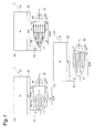
- Fig. 1 includes diagrams showing configurations of solid-state imaging devices according to a first embodiment of the present invention.
- the solid-state imaging device 1 shown in Fig. 1(a) includes an imaging area (IA) 10, a horizontal register unit (HR) 20, a corner register unit (CR) 30, a multiplication register unit (EMR) 40, an amplifier (AMP) 50, and an output port 60.
- IA imaging area
- HR horizontal register unit
- CR corner register unit
- EMR multiplication register unit
- AMP amplifier
- the horizontal register unit 20 corresponds to an output register described in the scope of claims
- the corner register unit 30 corresponds to an intermediate register described in the scope of claims.
- the imaging area 10 is for taking an image of incident light, and contains a plurality of pixel units.
- Each pixel unit has a photodiode that generates charge of an amount according to the amount of incident light, and a charge accumulating unit that accumulates the charge.
- Each pixel unit performs, in response to a clock having a periodic pulsed voltage, in-pixel charge transfer from the photodiode to the charge accumulating unit, charge transfer from the charge accumulating unit to the horizontal register unit 20, and the like.
- the horizontal register unit 20 includes a plurality of horizontal registers horizontally arrayed corresponding to every vertical line of the imaging area 10, and in response to a clock having a periodic pulsed voltage, sequentially transfers charges of each horizontal register to the corner register unit 30.
- the corner register unit 30 includes a plurality of registers that are connected in series, and in response to a clock having a periodic pulsed voltage, sequentially transfers charges sequentially transferred from the horizontal register unit 20 to the multiplication register unit 40.
- the multiplication register unit 40 includes a plurality of multiplication registers, multiplies the charges sequentially transferred from the corner register unit 30, and outputs the charges to the amplifier 50.
- Each multiplication register causes an energy potential deeper than that for normal transfer to be generated by being applied with a high voltage to its charge transfer channel layer, and uses a charge multiplication effect by an impact ionization effect. Since the charge multiplication effect by an impact ionization effect per one stage of multiplication register is small, the multiplication register unit 40 has approximately several hundred stages of multiplication registers, for example.
- the amplifier 50 amplifies as well as converts a charge transferred from the multiplication register unit 40 to a voltage signal, and outputs the signal to the output port 60.
- the multiplication register unit 40 exhibits a tapered shape that has a narrow width at an input terminal portion 41, and is gradually increased in width to both side portions 43 and 44 toward an output terminal portion 42.
- a part from the input terminal portion 41 to a middle portion 45 is tapered.
- a plurality of charge dispersion units 71 are disposed in this tapered part from the input terminal portion 41 to the middle portion 45.
- Each of the charge dispersion units 71 extends from the input terminal portion 41 or a tapered surface 46, 47 of the tapered shape to the middle portion 45, and the charge dispersion units 71 are arrayed separated from each other in the width direction perpendicular to a charge transfer direction.
- One end portion 71a of each charge dispersion unit 71 exhibits a shape along the tapered surface 46, 47, and is separated from the tapered surface 46, 47.
- the charge dispersion units 71 are made of a semiconductor material having a high resistance or an insulating material having insulating properties, as to be described later. Thus, the charge dispersion units 71 serve as regions that hinder charge transfer.
- a charge input from the input terminal portion 41 can be dispersed along the tapered surfaces 46 and 47 toward both side portions 43 and 44, and can be dispersed to a plurality of transfer channels formed dispersed in the width direction, which are transfer channels formed between the charge dispersion units 71. That is, the charge input from the input terminal portion 41 can be uniformly dispersed in the width direction.
- the charge dispersion units 71 may extend to the vicinity of the output terminal portion 42. That is, a multiplication register unit 140 may have, in place of the charge dispersion units 71, charge dispersion units 72 for which the charge dispersion units 71 extend to the vicinity of the output terminal portion 42 in the multiplication register unit 40, and a solid-state imaging device 101 may include the multiplication register unit 140 in place of the multiplication register unit 40 in the solid-state imaging device 1.
- Fig. 2 is a view showing a sectional view taken along a line II-II of Fig. 1(a)
- the multiplication register unit 40 is formed by a polysilicon (Poly-Si) electrode 205 formed on a layered structure for which a p-type epitaxial layer 202, an n-type channel layer 103, and an oxidation film 204 are sequentially stacked on a p-type substrate 201.
- a high-concentration p-type layer 206 is formed at both side portions 43 and 44 of the multiplication register unit 40, which are both side portions of the n-type channel layer 203.
- the n-type channel layer 203 is a charge transfer channel, where charge multiplication is to be performed.
- a plurality of charge dispersion units 71 are formed.
- the charge dispersion units 71 are formed of high-concentration n-type channel stop regions by dispersion of impurities. That is, the charge dispersion units 71 are formed of regions that have a high resistance and hinder charge transfer.
- p-type channel stop regions may be applied, or isolation regions having insulating properties may be applied.
- Fig. 3(a) is a view showing a configuration of a solid-state imaging device of a conventional example
- Fig. 3(b) is a sectional view taken along a line III-III shown in Fig. 3 (a) .
- the solid-state imaging device IX shown in Fig. 3 is different from the first embodiment in including a multiplication register unit 40X in place of the multiplication register unit 40 in the solid-state imaging device 1.
- the multiplication register unit 40X is different from the multiplication register unit 40 in the configuration exhibiting a substantially rectangular shape and having no charge dispersion units 71.
- charge has the property of moving the minimum distance of a transfer channel. Particularly, this property is remarkable in such a case of high-speed transfer before being spread by mutual charge repulsion as in the present embodiment. Moreover, since there is a corner, the potential is high inside the corner to produce a curve along the inside of the corner. Therefore, even if the multiplication register unit 40X is formed wide, the charge is concentrated to a part in the width direction of the multiplication register unit 40X, so that charge multiplication is locally performed in the charge register unit 40X (the arrow part in Fig. 3(a) ). As a result, there may be a case that the charge multiplication efficiency drops, the charge capacity is limited, and a local degradation in multiplication gain occurs.
- the solid-state imaging device 1 of the first embodiment since a charge input to the multiplication register unit 40 can be dispersed, by the charge dispersion units 71, in the width direction perpendicular to the transfer direction, local concentration of a transfer charge in the multiplication register unit 40 can be suppressed. Therefore, a drop in the charge multiplication efficiency, a limit in charge capacity, and a local degradation in multiplication gain can be suppressed in the multiplication register unit 40.
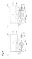
- Fig. 4 includes diagrams showing configurations of solid-state imaging devices according to a second embodiment of the present invention.
- the solid-state imaging device 1A shown in Fig. 4(a) is different from the first embodiment in an aspect of the configuration including a multiplication register unit 40A in place of the multiplication register unit 40 in the solid-state imaging device 1.
- Other aspects of the configuration of the solid-state imaging device 1A are the same as those of the solid-state imaging device 1.
- the multiplication register unit 40A is different from the multiplication register unit 40 in exhibiting a substantially rectangular shape in the multiplication register unit 40. Moreover, the multiplication register unit 40A is also different from the multiplication register unit 40 in having a wall 48. Other aspects of the configuration of the multiplication register unit 40A are the same as those of the multiplication register unit 40.
- the wall 48 is formed at an approximately half part of a side closer to the horizontal register 20 in the input terminal portion 41 of the multiplication register unit 40A.
- the same material as that of the charge dispersion units 71 can be applied to the material of the wall 48. Accordingly, charge can be led to a substantially central part of the input terminal portion 41, so that similar advantageous effects to those of the multiplication register unit 40 can be obtained.
- the charge dispersion units 71 may extend to the vicinity of the output terminal portion 42. That is, a multiplication register unit 140A may have, in place of the charge dispersion units 71, charge dispersion units 72 for which the charge dispersion units 71 extend to the vicinity of the output terminal portion 42 in the multiplication register unit 40A, and a solid-state imaging device 101A may include the multiplication register unit 140A in place of the multiplication register unit 40A in the solid-state imaging device 1A.
- the same advantages as those of the solid-state imaging device 1 of the first embodiment can be obtained.
- Fig. 5 includes diagrams showing configurations of solid-state imaging devices according to a third embodiment of the present invention.
- the solid-state imaging device 1B shown in Fig. 5(a) is different from the second embodiment in an aspect of the configuration including a multiplication register unit 40B in place of the multiplication register unit 40A in the solid-state imaging device 1A.
- Other aspects of the configuration of the solid-state imaging device 1B are the same as those of the solid-state imaging device 1A.
- the multiplication register unit 40B is different from the multiplication register unit 40A in that the charge dispersion units 71 do not extend to the middle portion 45 in the multiplication register unit 40A, that is, in having a plurality of charge dispersion units 73 shorter in length than the charge dispersion units 71.
- Other aspects of the configuration of the multiplication register unit 40B are the same as those of the multiplication register unit 40A.
- the charge dispersion unit 73 may be arrayed in a plural number separated from each other from the input terminal portion 41 toward the output terminal portion 42. That is, a multiplication register unit 140B may, in the multiplication register unit 40B, have a plurality of charge dispersion units 73 arrayed in the charge transfer direction as well as the width direction, and a solid-state imaging device 101B may include the multiplication register unit 140B in place of the multiplication register unit 40B in the solid-state imaging device 1B.
- the charge dispersion units 73 neighboring in the charge transfer direction are disposed so as not to overlap with each other in the charge transfer direction. Accordingly, a charge that has arrived transferred between the charge dispersion units 73 of a former stage can be dispersed by the charge dispersion units 73 of a latter stage.
- a charge input from the input terminal unit 41 is, by being dispersed into two parts at every charge dispersion unit 73, gradually uniformly dispersed in the width direction.
- the same advantages as those of the solid-state imaging device 1A of the second embodiment can be obtained.
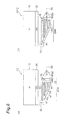
- Fig. 6 includes diagrams showing configurations of solid-state imaging devices according to a fourth embodiment of the present invention.
- the solid-state imaging device 1C shown in Fig. 6(a) is different from the first embodiment in an aspect of the configuration including a multiplication register unit 40C in place of the multiplication register unit 40 in the solid-state imaging device 1.
- Other aspects of the configuration of the solid-state imaging device 1C are the same as those of the solid-state imaging device 1.
- the multiplication register unit 40C exhibits a tapered shape that has a narrow width at the input terminal portion 41, and is gradually increased in width to one side portion 44 toward the output terminal portion 42.
- a part from the input terminal portion 41 to the middle portion 45 is tapered.
- a plurality of charge dispersion units 75 are disposed in this tapered part from the input terminal portion 41 to the middle portion 45.
- Each of the charge dispersion units 75 extends from the input terminal portion 41 or a tapered surface 47 of the tapered shape to the middle portion 45, and the charge dispersion units 75 are arrayed separated from each other in the width direction.
- One end portion 75a of each charge dispersion unit 75 exhibits a shape along the tapered surface 47, and is separated from the tapered surface 47.
- the same material as that of the charge dispersion units 71 is applied to the charge dispersion units 75.
- a charge input from the input terminal portion 41 can be dispersed along the tapered surface 47 toward one side portion 44, and can be dispersed to a plurality of transfer channels formed dispersed in the width direction, which are transfer channels formed between the charge dispersion units 75. That is, the charge input from the input terminal portion 41 can be uniformly dispersed in the width direction.
- the charge dispersion units 75 may extend to the vicinity of the output terminal portion 42. That is, a multiplication register unit 140C may have, in place of the charge dispersion units 75, charge dispersion units 76 for which the charge dispersion units 75 extend to the vicinity of the output terminal portion 42 in the multiplication register unit 40C, and a solid-state imaging device 101C may include the multiplication register unit 140C in place of the multiplication register unit 40C in the solid-state imaging device 1C.
- solid-state imaging device 1C of the fourth embodiment and the solid-state imaging device 101C of a modification of the fourth embodiment, the same advantages as those of the solid-state imaging device 1 of the first embodiment can be obtained.
- Fig. 7 includes diagrams showing configurations of solid-state imaging devices according to a fifth embodiment or the present invention.
- the solid-state imaging device 1D shown in Fig. 7(a) is different from the fourth embodiment in an aspect of the configuration including a multiplication register unit 40D in place of the multiplication register unit 40C in the solid-state imaging device 1C.
- Other aspects of the configuration of the solid-state imaging device 1D are the same as those of the solid-state imaging device 1C.
- the multiplication register unit 40D is different from the multiplication register unit 40C in exhibiting a substantially rectangular shape in the multiplication register unit 40C. Other aspects of the configuration of the multiplication register unit 40D are the same as those of the multiplication register unit 40C.
- the charge dispersion units 75 may extend to the vicinity of the output terminal portion 42. That is, a multiplication register unit 140D may have, in place of the charge dispersion units 75, charge dispersion units 76 for which the charge dispersion units 75 extend to the vicinity of the output terminal portion 42 in the multiplication register unit 40D, and a solid-state imaging device 101D may include the multiplication register unit 140D in place of the multiplication register unit 40D in the solid-state imaging device 1D.
- the same advantages as those of the solid-state imaging device 1C of the fourth embodiment can be obtained.
- Fig. 8 includes diagrams showing configurations of solid-state imaging devices according to a sixth embodiment of the present invention.
- the solid-state imaging device 1E shown in Fig. 8(a) is different from the fifth embodiment in an aspect of the configuration including a multiplication register unit 40E in place of the multiplication register unit 40D in the solid-state imaging device 1D.
- Other aspects of the configuration of the solid-state imaging device 1E are the same as those of the solid-state imaging device 1D.
- the multiplication register unit 40E is different from the multiplication register unit 40D in that the charge dispersion units 75 do not extend to the middle portion 45 in the multiplication register unit 40D, that is, in having a plurality of charge dispersion units 77 shorter in length than the charge dispersion units 75.
- Other aspects of the configuration of the multiplication register unit 40E are the same as those of the multiplication register unit 40D.
- the charge dispersion unit 77 may be arrayed in a plural number separated from each other from the input terminal portion 41 toward the output terminal portion 42. That is, a multiplication register unit 140E may, in the multiplication register unit 40E, have a plurality of charge dispersion units 77 arrayed in the charge transfer direction as well as the width direction, and a solid-state imaging device 101E may include the multiplication register unit 140E in place of the multiplication register unit 40E in the solid-state imaging device 1E.
- the same advantages as those of the solid-state imaging device 1D of the fifth embodiment can be obtained.
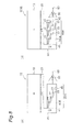
- Fig. 9 includes diagrams showing configurations of solid-state imaging devices according to a seventh embodiment of the present invention.
- the solid-state imaging device 1F shown in Fig. 9(a) is different from the fifth embodiment in an aspect of the configuration including a multiplication register unit 40F in place of the multiplication register unit 40D in the solid-state imaging device 1D.
- Other aspects of the configuration of the solid-state imaging device 1F are the same as those of the solid-state imaging device 1D.
- the multiplication register unit 40F is different from the multiplication register unit 40D in including a plurality of charge dispersion units 79 in place of the charge dispersion units 75 in the multiplication register unit 40D.
- Each charge dispersion unit 79 exhibits a substantially rectangular shape, and the charge dispersion units 79 are arrayed separated from each other in the width direction of the multiplication register unit 40F.
- each charge dispersion unit 79 may be in a substantially polygonal shape without being limited to a substantially triangular shape.
- the charge dispersion units 79 are arrayed separated from each other from the input terminal portion 41 toward the middle portion 45.
- the charge dispersion units 79 are disposed, in the multiplication register unit 40F, at approximately half of the side closer to the input terminal portion 41.
- the same material as that of the charge dispersion units 71 can be applied to the charge dispersion units 79.
- the charge dispersion units 79 neighboring in the charge transfer direction are disposed so as not to overlap with each other in the charge transfer direction. Accordingly, a charge that has arrived transferred between the charge dispersion units 79 of a former stage can be dispersed by the charge dispersion units 79 of a latter stage.
- a charge input from the input terminal unit 41 is, by being dispersed into two parts at every charge dispersion unit 79, gradually uniformly dispersed in the width direction.
- the charge dispersion unit 79 may be arrayed in a plural number separated from each other from the input terminal portion 41 toward the output terminal portion 42. That is, a multiplication register unit 140F may, in the multiplication register unit 40F, have a plurality of charge dispersion units 79 arrayed separated as a whole from each other, and a solid-state imaging device 101F may include the multiplication register unit 140F in place of the multiplication register unit 40F in the solid-state imaging device 1F. Moreover, as described above, it is preferable that the charge dispersion units 79 neighboring in the charge transfer direction are disposed so as not to overlap with each other in the charge transfer direction.
- solid-state imaging device 1F of the seventh embodiment and the solid-state imaging device 10 1F of a modification of the seventh embodiment, the same advantages as those of the solid-state imaging device 1D of the fifth embodiment can be obtained.
- Fig. 10 includes diagrams showing configurations of solid-state imaging devices according to an eighth embodiment of the present invention.
- the solid-state imaging device 1G shown in Fig. 10 is different from the seventh embodiment in an aspect of the configuration including a multiplication register unit 40G in place of the multiplication register unit 40F in the solid-state imaging device 1F.
- Other aspects of the configuration of the solid-state imaging device 1G are the same as those of the solid-state imaging device 1F.
- the multiplication register unit 40G is different from the multiplication register unit 40F in including a plurality of charge dispersion units 81 each exhibiting a substantially circular shape in place of the charge dispersion units 79 in the multiplication register unit 40F. Other aspects of the configuration of the multiplication register unit 40G are the same as those of the multiplication register unit 40F.
- solid-state imaging device 1G of the eighth embodiment and the solid-state imaging device 101G of a modification of the eighth embodiment, the same advantages as those of the solid-state imaging device 1F of the seventh embodiment can be obtained.
- charge dispersion means may be provided at a previous stage of the multiplication register unit.
- Fig. 11 includes diagrams showing configurations of solid-state imaging devices according to a ninth embodiment of the present invention.
- the solid-state imaging device 1H shown in Fig. 11(a) is different from the first embodiment in an aspect of the configuration including a corner register unit 30H and a multiplication register unit 40H in place of the corner register unit 30 and the multiplication register unit 40 in the solid-state imaging device 1.
- Other aspects of the configuration of the solid-state imaging device 1H are the same as those of the solid-state imaging device 1.
- the corner register unit 30H is different from the corner register unit 30 in having a plurality of charge dispersion units 31 in the corner register unit 30.
- the charge dispersion units 31 extend in the charge transfer direction at the side of an output portion 32 in the corner register unit 30H, and are arrayed separated from each other in the width direction.
- the same material as that of the charge dispersion units 71 can be applied to the charge dispersion units 31.
- the multiplication register unit 40H is a normal multiplication register unit not having the above-described charge dispersion units.
- a plurality of charge dispersion units 83 may be formed so as to extend the charge dispersion units 31 in the multiplication register unit 40H. That is, a multiplication register unit 140H may, in the multiplication register unit 40H, have the charge dispersion units 83 extended from the input terminal portion 41 to the vicinity of the output terminal unit 42 and disposed separated from each other in the width direction, and a solid-state imaging device 101H may include the multiplication register unit 140H in place of the multiplication register unit 40H in the solid-state imaging device 1H.
- a charge to be input to the multiplication register unit 40H is dispersed in the width direction by the charge dispersion units 31 at the side of the output unit 32 of the corner register unit 30H located at a previous stage of the multiplication register unit 40H. Therefore, also in the solid-state imaging device 1H of the ninth embodiment, similar advantages to those of the solid-state imaging device 1 of the first embodiment can be obtained.
- a charge dispersion effect of the charge dispersion units 31 of the corner register unit 30H described above can be retained by the charge dispersion units 83 of the multiplication register unit 40H.
- Fig. 12 is a diagram showing a configuration of a solid-state imaging device according to a tenth embodiment of the present invention.
- the solid-state imaging device 1I shown in Fig. 12 is different from the ninth embodiment in an aspect of the configuration including a corner register unit 301 in place of the corner register unit 30H in the solid-state imaging device 1H.
- Other aspects of the configuration of the solid-state imaging device 1I are the same as those of the solid-state imaging device 1H.
- the corner register unit 30I is different from the corner register unit 30H in having charge dispersion units 35 and 36 in place of the charge dispersion units 31 in the corner register unit 30H.
- the charge dispersion unit 35 is a drive electrode at the side of a side portion 37 where a transfer charge is concentrated
- the charge dispersion unit 36 is a drive electrode at the side of the other side portion 38, that is, the side portion 38 where the density of transfer charge is low.
- a drive clock voltage greater than that to the charge dispersion unit 35 being input to the charge dispersion unit 36
- a charge induction effect at the side of the side portion 38 where the density of transfer charge is low can be increased.
- the transfer charge concentrated to the side of the side portion 37 can be dispersed to the side of the side portion 38, that is, in the width direction.
- the charge dispersion units 35 and 36 may serve also as electrodes for normal charge transfer in the corner register unit 301.
- a transfer charge concentrated to the side of the side portion 37 of the corner register unit 30I can be dispersed by the charge dispersion units 35 and 36 to the side portion 38 where the charge density low, that is, in the width direction, so that the charge can be dispersed in the width direction before being input to the charge register unit 40H. Therefore, also in the solid-state imaging device 1H of the ninth embodiment, similar advantages to those of the solid-state imaging device 1 of the first embodiment can be obtained.
- charge dispersion units (drive electrodes) similar to the charge dispersion units 35 and 36 may be formed in the multiplication register unit 40H. That is, the charge dispersion units (drive electrodes) may be formed at both side portions 43 and 44 of the multiplication register unit 40H, and a drive clock voltage greater than that to the charge dispersion unit (drive electrode) at the side of the side portion 43 where a transfer charge is concentrated may be input to the charge dispersion unit (drive electrode) at the side of the side portion 43 where the density of transfer charge is low.
- charge induction effect at the side of the side portion 44 where the density of transfer charge is low can be increased, so that the charge transfer concentrated to the side of the side portion 43 can be dispersed to the side portion 44, that is, in the width direction.
- these charge dispersion units may serve also as electrodes for normal charge transfer and charge multiplication in the corner register unit 40H.
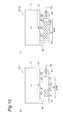
- channel stop regions 91 by a LOGOS (Local Oxidation of Silicon) method shown in Fig. 13(a) , channel regions with a shallow energy potential due to a change in film thickness of a gate SiO 2 film shown in Fig. 13(b) , that is, channel regions 92 that hinder charge transfer, and the like can be applied.
- LOGOS Local Oxidation of Silicon
- Fig. 14 shows a configuration of a solid-state imaging device of a conventional example where charge transfer is not folded back.
- the present invention can be applied to a use for suppressing local concentration of a transfer charge in the multiplication register unit.
Landscapes
- Engineering & Computer Science (AREA)
- Multimedia (AREA)
- Signal Processing (AREA)
- Solid State Image Pick-Up Elements (AREA)
- Transforming Light Signals Into Electric Signals (AREA)
Applications Claiming Priority (2)
| Application Number | Priority Date | Filing Date | Title |
|---|---|---|---|
| JP2009020200A JP5330001B2 (ja) | 2009-01-30 | 2009-01-30 | 固体撮像装置 |
| PCT/JP2010/050819 WO2010087289A1 (ja) | 2009-01-30 | 2010-01-22 | 固体撮像装置 |
Publications (3)
| Publication Number | Publication Date |
|---|---|
| EP2385697A1 true EP2385697A1 (de) | 2011-11-09 |
| EP2385697A4 EP2385697A4 (de) | 2013-02-20 |
| EP2385697B1 EP2385697B1 (de) | 2017-03-01 |
Family
ID=42395551
Family Applications (1)
| Application Number | Title | Priority Date | Filing Date |
|---|---|---|---|
| EP10735758.4A Not-in-force EP2385697B1 (de) | 2009-01-30 | 2010-01-22 | Festkörperabbildungsvorrichtung |
Country Status (7)
| Country | Link |
|---|---|
| US (1) | US8599296B2 (de) |
| EP (1) | EP2385697B1 (de) |
| JP (1) | JP5330001B2 (de) |
| KR (1) | KR101614567B1 (de) |
| CN (1) | CN102301695B (de) |
| TW (1) | TWI519159B (de) |
| WO (1) | WO2010087289A1 (de) |
Families Citing this family (1)
| Publication number | Priority date | Publication date | Assignee | Title |
|---|---|---|---|---|
| CN103698018B (zh) * | 2013-12-20 | 2016-06-29 | 北京理工大学 | 一种带电子倍增的铂硅红外焦平面探测器 |
Family Cites Families (16)
| Publication number | Priority date | Publication date | Assignee | Title |
|---|---|---|---|---|
| FR2441961A1 (fr) * | 1978-11-17 | 1980-06-13 | Thomson Csf | Filtre a transfert de charges electriques, programmable numeriquement |
| GB2323471B (en) | 1997-03-22 | 2002-04-17 | Eev Ltd | CCd imagers |
| US6278142B1 (en) * | 1999-08-30 | 2001-08-21 | Isetex, Inc | Semiconductor image intensifier |
| JP5026641B2 (ja) * | 2000-04-28 | 2012-09-12 | テキサス インスツルメンツ インコーポレイテッド | 固体撮像センサ |
| US7420605B2 (en) * | 2001-01-18 | 2008-09-02 | E2V Technologies (Uk) Limited | Solid state imager arrangements |
| GB2371403B (en) * | 2001-01-18 | 2005-07-27 | Marconi Applied Techn Ltd | Solid state imager arrangements |
| JP2003009000A (ja) | 2001-06-21 | 2003-01-10 | Fuji Photo Film Co Ltd | 撮像装置 |
| US20050029553A1 (en) * | 2003-08-04 | 2005-02-10 | Jaroslav Hynecek | Clocked barrier virtual phase charge coupled device image sensor |
| GB2413007A (en) * | 2004-04-07 | 2005-10-12 | E2V Tech Uk Ltd | Multiplication register for amplifying signal charge |
| GB0503827D0 (en) * | 2005-02-24 | 2005-04-06 | E2V Tech Uk Ltd | Enhanced spectral range imaging sensor |
| JP4958602B2 (ja) * | 2007-03-30 | 2012-06-20 | 富士フイルム株式会社 | 撮像装置及びその画像合成方法 |
| GB0717484D0 (en) * | 2007-09-07 | 2007-10-17 | E2V Tech Uk Ltd | Gain measurement method |
| JP5237843B2 (ja) * | 2009-01-30 | 2013-07-17 | 浜松ホトニクス株式会社 | 固体撮像装置 |
| JP5270392B2 (ja) * | 2009-01-30 | 2013-08-21 | 浜松ホトニクス株式会社 | 固体撮像装置 |
| JP5243984B2 (ja) * | 2009-01-30 | 2013-07-24 | 浜松ホトニクス株式会社 | 電子増倍機能内蔵型の固体撮像素子 |
| JP5243983B2 (ja) * | 2009-01-30 | 2013-07-24 | 浜松ホトニクス株式会社 | 電子増倍機能内蔵型の固体撮像素子 |
-
2009
- 2009-01-30 JP JP2009020200A patent/JP5330001B2/ja not_active Expired - Fee Related
-
2010
- 2010-01-22 CN CN201080006073.1A patent/CN102301695B/zh not_active Expired - Fee Related
- 2010-01-22 KR KR1020117007771A patent/KR101614567B1/ko not_active Expired - Fee Related
- 2010-01-22 EP EP10735758.4A patent/EP2385697B1/de not_active Not-in-force
- 2010-01-22 US US13/139,855 patent/US8599296B2/en not_active Expired - Fee Related
- 2010-01-22 WO PCT/JP2010/050819 patent/WO2010087289A1/ja not_active Ceased
- 2010-01-27 TW TW099102303A patent/TWI519159B/zh not_active IP Right Cessation
Also Published As
| Publication number | Publication date |
|---|---|
| US8599296B2 (en) | 2013-12-03 |
| JP2010178179A (ja) | 2010-08-12 |
| CN102301695B (zh) | 2015-02-11 |
| US20110254989A1 (en) | 2011-10-20 |
| WO2010087289A1 (ja) | 2010-08-05 |
| KR101614567B1 (ko) | 2016-04-21 |
| JP5330001B2 (ja) | 2013-10-30 |
| KR20110105763A (ko) | 2011-09-27 |
| EP2385697A4 (de) | 2013-02-20 |
| CN102301695A (zh) | 2011-12-28 |
| EP2385697B1 (de) | 2017-03-01 |
| TWI519159B (zh) | 2016-01-21 |
| TW201034455A (en) | 2010-09-16 |
Similar Documents
| Publication | Publication Date | Title |
|---|---|---|
| EP2279614B1 (de) | Festkörper-bildsensor mit reduzierter überstrahlung und farbverwischung | |
| EP2752877B1 (de) | Einheitspixel und lichtempfangselement für einen bildsensor | |
| JP6595750B2 (ja) | 固体撮像装置及び撮像システム | |
| CN101997016B (zh) | 具有含多个沟道子区域的传输栅极的图像传感器 | |
| CN102655158B (zh) | 固态成像器件 | |
| US8154055B2 (en) | CMOS image sensor and method for fabricating the same | |
| US20060081957A1 (en) | Solid-state imaging device | |
| US9190439B2 (en) | Solid-state image pickup device | |
| CN102956658A (zh) | 固态成像设备、固态成像设备的制造方法及电子设备 | |
| US12349441B2 (en) | Semiconductor device and semiconductor device manufacturing method, and image capturing device | |
| CN120092509A (zh) | 成像装置 | |
| EP2385697A1 (de) | Festkörperabbildungsvorrichtung | |
| JP2008177357A (ja) | 固体撮像素子 | |
| JP2011054596A (ja) | Ccdイメージセンサ | |
| JP4900404B2 (ja) | 固体撮像素子及びその駆動方法 | |
| US9437648B2 (en) | Solid-state image pickup device | |
| KR20070050576A (ko) | 이미지 센서 | |
| KR100937673B1 (ko) | Cmos 이미지 센서 | |
| KR20100079172A (ko) | 씨모스 이미지 센서와 그 제조 방법 | |
| JP2010225769A (ja) | 固体撮像素子及び撮像装置 | |
| KR20070071019A (ko) | 시모스 이미지 센서 | |
| JP2010287799A (ja) | 固体撮像装置 | |
| JP2004281443A (ja) | 固体撮像装置 | |
| JP2006344800A (ja) | 固体撮像素子 | |
| JP2010050710A (ja) | 固体撮像素子 |
Legal Events
| Date | Code | Title | Description |
|---|---|---|---|
| PUAI | Public reference made under article 153(3) epc to a published international application that has entered the european phase |
Free format text: ORIGINAL CODE: 0009012 |
|
| 17P | Request for examination filed |
Effective date: 20110608 |
|
| AK | Designated contracting states |
Kind code of ref document: A1 Designated state(s): AT BE BG CH CY CZ DE DK EE ES FI FR GB GR HR HU IE IS IT LI LT LU LV MC MK MT NL NO PL PT RO SE SI SK SM TR |
|
| DAX | Request for extension of the european patent (deleted) | ||
| A4 | Supplementary search report drawn up and despatched |
Effective date: 20130118 |
|
| RIC1 | Information provided on ipc code assigned before grant |
Ipc: H01L 27/148 20060101ALI20130114BHEP Ipc: H04N 5/335 20110101AFI20130114BHEP |
|
| 17Q | First examination report despatched |
Effective date: 20160121 |
|
| GRAP | Despatch of communication of intention to grant a patent |
Free format text: ORIGINAL CODE: EPIDOSNIGR1 |
|
| INTG | Intention to grant announced |
Effective date: 20160926 |
|
| GRAS | Grant fee paid |
Free format text: ORIGINAL CODE: EPIDOSNIGR3 |
|
| GRAA | (expected) grant |
Free format text: ORIGINAL CODE: 0009210 |
|
| AK | Designated contracting states |
Kind code of ref document: B1 Designated state(s): AT BE BG CH CY CZ DE DK EE ES FI FR GB GR HR HU IE IS IT LI LT LU LV MC MK MT NL NO PL PT RO SE SI SK SM TR |
|
| REG | Reference to a national code |
Ref country code: GB Ref legal event code: FG4D |
|
| REG | Reference to a national code |
Ref country code: AT Ref legal event code: REF Ref document number: 872533 Country of ref document: AT Kind code of ref document: T Effective date: 20170315 Ref country code: CH Ref legal event code: EP |
|
| REG | Reference to a national code |
Ref country code: IE Ref legal event code: FG4D |
|
| REG | Reference to a national code |
Ref country code: DE Ref legal event code: R096 Ref document number: 602010040383 Country of ref document: DE |
|
| REG | Reference to a national code |
Ref country code: NL Ref legal event code: MP Effective date: 20170301 |
|
| REG | Reference to a national code |
Ref country code: LT Ref legal event code: MG4D |
|
| REG | Reference to a national code |
Ref country code: AT Ref legal event code: MK05 Ref document number: 872533 Country of ref document: AT Kind code of ref document: T Effective date: 20170301 |
|
| PG25 | Lapsed in a contracting state [announced via postgrant information from national office to epo] |
Ref country code: LT Free format text: LAPSE BECAUSE OF FAILURE TO SUBMIT A TRANSLATION OF THE DESCRIPTION OR TO PAY THE FEE WITHIN THE PRESCRIBED TIME-LIMIT Effective date: 20170301 Ref country code: FI Free format text: LAPSE BECAUSE OF FAILURE TO SUBMIT A TRANSLATION OF THE DESCRIPTION OR TO PAY THE FEE WITHIN THE PRESCRIBED TIME-LIMIT Effective date: 20170301 Ref country code: HR Free format text: LAPSE BECAUSE OF FAILURE TO SUBMIT A TRANSLATION OF THE DESCRIPTION OR TO PAY THE FEE WITHIN THE PRESCRIBED TIME-LIMIT Effective date: 20170301 Ref country code: NO Free format text: LAPSE BECAUSE OF FAILURE TO SUBMIT A TRANSLATION OF THE DESCRIPTION OR TO PAY THE FEE WITHIN THE PRESCRIBED TIME-LIMIT Effective date: 20170601 Ref country code: GR Free format text: LAPSE BECAUSE OF FAILURE TO SUBMIT A TRANSLATION OF THE DESCRIPTION OR TO PAY THE FEE WITHIN THE PRESCRIBED TIME-LIMIT Effective date: 20170602 |
|
| PG25 | Lapsed in a contracting state [announced via postgrant information from national office to epo] |
Ref country code: AT Free format text: LAPSE BECAUSE OF FAILURE TO SUBMIT A TRANSLATION OF THE DESCRIPTION OR TO PAY THE FEE WITHIN THE PRESCRIBED TIME-LIMIT Effective date: 20170301 Ref country code: LV Free format text: LAPSE BECAUSE OF FAILURE TO SUBMIT A TRANSLATION OF THE DESCRIPTION OR TO PAY THE FEE WITHIN THE PRESCRIBED TIME-LIMIT Effective date: 20170301 Ref country code: ES Free format text: LAPSE BECAUSE OF FAILURE TO SUBMIT A TRANSLATION OF THE DESCRIPTION OR TO PAY THE FEE WITHIN THE PRESCRIBED TIME-LIMIT Effective date: 20170301 Ref country code: BG Free format text: LAPSE BECAUSE OF FAILURE TO SUBMIT A TRANSLATION OF THE DESCRIPTION OR TO PAY THE FEE WITHIN THE PRESCRIBED TIME-LIMIT Effective date: 20170601 Ref country code: SE Free format text: LAPSE BECAUSE OF FAILURE TO SUBMIT A TRANSLATION OF THE DESCRIPTION OR TO PAY THE FEE WITHIN THE PRESCRIBED TIME-LIMIT Effective date: 20170301 |
|
| PG25 | Lapsed in a contracting state [announced via postgrant information from national office to epo] |
Ref country code: NL Free format text: LAPSE BECAUSE OF FAILURE TO SUBMIT A TRANSLATION OF THE DESCRIPTION OR TO PAY THE FEE WITHIN THE PRESCRIBED TIME-LIMIT Effective date: 20170301 |
|
| PG25 | Lapsed in a contracting state [announced via postgrant information from national office to epo] |
Ref country code: SK Free format text: LAPSE BECAUSE OF FAILURE TO SUBMIT A TRANSLATION OF THE DESCRIPTION OR TO PAY THE FEE WITHIN THE PRESCRIBED TIME-LIMIT Effective date: 20170301 Ref country code: EE Free format text: LAPSE BECAUSE OF FAILURE TO SUBMIT A TRANSLATION OF THE DESCRIPTION OR TO PAY THE FEE WITHIN THE PRESCRIBED TIME-LIMIT Effective date: 20170301 Ref country code: RO Free format text: LAPSE BECAUSE OF FAILURE TO SUBMIT A TRANSLATION OF THE DESCRIPTION OR TO PAY THE FEE WITHIN THE PRESCRIBED TIME-LIMIT Effective date: 20170301 Ref country code: CZ Free format text: LAPSE BECAUSE OF FAILURE TO SUBMIT A TRANSLATION OF THE DESCRIPTION OR TO PAY THE FEE WITHIN THE PRESCRIBED TIME-LIMIT Effective date: 20170301 |
|
| PG25 | Lapsed in a contracting state [announced via postgrant information from national office to epo] |
Ref country code: IS Free format text: LAPSE BECAUSE OF FAILURE TO SUBMIT A TRANSLATION OF THE DESCRIPTION OR TO PAY THE FEE WITHIN THE PRESCRIBED TIME-LIMIT Effective date: 20170701 Ref country code: SM Free format text: LAPSE BECAUSE OF FAILURE TO SUBMIT A TRANSLATION OF THE DESCRIPTION OR TO PAY THE FEE WITHIN THE PRESCRIBED TIME-LIMIT Effective date: 20170301 Ref country code: PL Free format text: LAPSE BECAUSE OF FAILURE TO SUBMIT A TRANSLATION OF THE DESCRIPTION OR TO PAY THE FEE WITHIN THE PRESCRIBED TIME-LIMIT Effective date: 20170301 Ref country code: PT Free format text: LAPSE BECAUSE OF FAILURE TO SUBMIT A TRANSLATION OF THE DESCRIPTION OR TO PAY THE FEE WITHIN THE PRESCRIBED TIME-LIMIT Effective date: 20170703 |
|
| REG | Reference to a national code |
Ref country code: DE Ref legal event code: R097 Ref document number: 602010040383 Country of ref document: DE |
|
| REG | Reference to a national code |
Ref country code: FR Ref legal event code: PLFP Year of fee payment: 9 |
|
| PLBE | No opposition filed within time limit |
Free format text: ORIGINAL CODE: 0009261 |
|
| STAA | Information on the status of an ep patent application or granted ep patent |
Free format text: STATUS: NO OPPOSITION FILED WITHIN TIME LIMIT |
|
| PG25 | Lapsed in a contracting state [announced via postgrant information from national office to epo] |
Ref country code: DK Free format text: LAPSE BECAUSE OF FAILURE TO SUBMIT A TRANSLATION OF THE DESCRIPTION OR TO PAY THE FEE WITHIN THE PRESCRIBED TIME-LIMIT Effective date: 20170301 |
|
| 26N | No opposition filed |
Effective date: 20171204 |
|
| PG25 | Lapsed in a contracting state [announced via postgrant information from national office to epo] |
Ref country code: IT Free format text: LAPSE BECAUSE OF FAILURE TO SUBMIT A TRANSLATION OF THE DESCRIPTION OR TO PAY THE FEE WITHIN THE PRESCRIBED TIME-LIMIT Effective date: 20170301 Ref country code: SI Free format text: LAPSE BECAUSE OF FAILURE TO SUBMIT A TRANSLATION OF THE DESCRIPTION OR TO PAY THE FEE WITHIN THE PRESCRIBED TIME-LIMIT Effective date: 20170301 |
|
| REG | Reference to a national code |
Ref country code: CH Ref legal event code: PL |
|
| PG25 | Lapsed in a contracting state [announced via postgrant information from national office to epo] |
Ref country code: LU Free format text: LAPSE BECAUSE OF NON-PAYMENT OF DUE FEES Effective date: 20180122 |
|
| REG | Reference to a national code |
Ref country code: IE Ref legal event code: MM4A |
|
| REG | Reference to a national code |
Ref country code: BE Ref legal event code: MM Effective date: 20180131 |
|
| PG25 | Lapsed in a contracting state [announced via postgrant information from national office to epo] |
Ref country code: BE Free format text: LAPSE BECAUSE OF NON-PAYMENT OF DUE FEES Effective date: 20180131 Ref country code: CH Free format text: LAPSE BECAUSE OF NON-PAYMENT OF DUE FEES Effective date: 20180131 Ref country code: LI Free format text: LAPSE BECAUSE OF NON-PAYMENT OF DUE FEES Effective date: 20180131 |
|
| PG25 | Lapsed in a contracting state [announced via postgrant information from national office to epo] |
Ref country code: IE Free format text: LAPSE BECAUSE OF NON-PAYMENT OF DUE FEES Effective date: 20180122 |
|
| PG25 | Lapsed in a contracting state [announced via postgrant information from national office to epo] |
Ref country code: MC Free format text: LAPSE BECAUSE OF FAILURE TO SUBMIT A TRANSLATION OF THE DESCRIPTION OR TO PAY THE FEE WITHIN THE PRESCRIBED TIME-LIMIT Effective date: 20170301 |
|
| PG25 | Lapsed in a contracting state [announced via postgrant information from national office to epo] |
Ref country code: MT Free format text: LAPSE BECAUSE OF NON-PAYMENT OF DUE FEES Effective date: 20180122 |
|
| PGFP | Annual fee paid to national office [announced via postgrant information from national office to epo] |
Ref country code: FR Payment date: 20191216 Year of fee payment: 11 |
|
| PG25 | Lapsed in a contracting state [announced via postgrant information from national office to epo] |
Ref country code: TR Free format text: LAPSE BECAUSE OF FAILURE TO SUBMIT A TRANSLATION OF THE DESCRIPTION OR TO PAY THE FEE WITHIN THE PRESCRIBED TIME-LIMIT Effective date: 20170301 |
|
| PGFP | Annual fee paid to national office [announced via postgrant information from national office to epo] |
Ref country code: GB Payment date: 20200115 Year of fee payment: 11 Ref country code: DE Payment date: 20200107 Year of fee payment: 11 |
|
| PG25 | Lapsed in a contracting state [announced via postgrant information from national office to epo] |
Ref country code: HU Free format text: LAPSE BECAUSE OF FAILURE TO SUBMIT A TRANSLATION OF THE DESCRIPTION OR TO PAY THE FEE WITHIN THE PRESCRIBED TIME-LIMIT; INVALID AB INITIO Effective date: 20100122 |
|
| PG25 | Lapsed in a contracting state [announced via postgrant information from national office to epo] |
Ref country code: MK Free format text: LAPSE BECAUSE OF NON-PAYMENT OF DUE FEES Effective date: 20170301 Ref country code: CY Free format text: LAPSE BECAUSE OF FAILURE TO SUBMIT A TRANSLATION OF THE DESCRIPTION OR TO PAY THE FEE WITHIN THE PRESCRIBED TIME-LIMIT Effective date: 20170301 |
|
| REG | Reference to a national code |
Ref country code: DE Ref legal event code: R119 Ref document number: 602010040383 Country of ref document: DE |
|
| GBPC | Gb: european patent ceased through non-payment of renewal fee |
Effective date: 20210122 |
|
| PG25 | Lapsed in a contracting state [announced via postgrant information from national office to epo] |
Ref country code: FR Free format text: LAPSE BECAUSE OF NON-PAYMENT OF DUE FEES Effective date: 20210131 |
|
| PG25 | Lapsed in a contracting state [announced via postgrant information from national office to epo] |
Ref country code: DE Free format text: LAPSE BECAUSE OF NON-PAYMENT OF DUE FEES Effective date: 20210803 Ref country code: GB Free format text: LAPSE BECAUSE OF NON-PAYMENT OF DUE FEES Effective date: 20210122 |