EP2383784A1 - Method for manufacturing silicon carbide semiconductor element - Google Patents
Method for manufacturing silicon carbide semiconductor element Download PDFInfo
- Publication number
- EP2383784A1 EP2383784A1 EP09834272A EP09834272A EP2383784A1 EP 2383784 A1 EP2383784 A1 EP 2383784A1 EP 09834272 A EP09834272 A EP 09834272A EP 09834272 A EP09834272 A EP 09834272A EP 2383784 A1 EP2383784 A1 EP 2383784A1
- Authority
- EP
- European Patent Office
- Prior art keywords
- electrode
- silicon carbide
- type
- schottky
- sic semiconductor
- Prior art date
- Legal status (The legal status is an assumption and is not a legal conclusion. Google has not performed a legal analysis and makes no representation as to the accuracy of the status listed.)
- Withdrawn
Links
Images



Classifications
-
- H—ELECTRICITY
- H10—SEMICONDUCTOR DEVICES; ELECTRIC SOLID-STATE DEVICES NOT OTHERWISE PROVIDED FOR
- H10D—INORGANIC ELECTRIC SEMICONDUCTOR DEVICES
- H10D8/00—Diodes
- H10D8/60—Schottky-barrier diodes
-
- H—ELECTRICITY
- H10—SEMICONDUCTOR DEVICES; ELECTRIC SOLID-STATE DEVICES NOT OTHERWISE PROVIDED FOR
- H10D—INORGANIC ELECTRIC SEMICONDUCTOR DEVICES
- H10D62/00—Semiconductor bodies, or regions thereof, of devices having potential barriers
- H10D62/80—Semiconductor bodies, or regions thereof, of devices having potential barriers characterised by the materials
- H10D62/83—Semiconductor bodies, or regions thereof, of devices having potential barriers characterised by the materials being Group IV materials, e.g. B-doped Si or undoped Ge
- H10D62/832—Semiconductor bodies, or regions thereof, of devices having potential barriers characterised by the materials being Group IV materials, e.g. B-doped Si or undoped Ge being Group IV materials comprising two or more elements, e.g. SiGe
- H10D62/8325—Silicon carbide
-
- H—ELECTRICITY
- H10—SEMICONDUCTOR DEVICES; ELECTRIC SOLID-STATE DEVICES NOT OTHERWISE PROVIDED FOR
- H10D—INORGANIC ELECTRIC SEMICONDUCTOR DEVICES
- H10D64/00—Electrodes of devices having potential barriers
- H10D64/01—Manufacture or treatment
- H10D64/011—Manufacture or treatment of electrodes ohmically coupled to a semiconductor
- H10D64/0111—Manufacture or treatment of electrodes ohmically coupled to a semiconductor to Group IV semiconductors
- H10D64/0115—Manufacture or treatment of electrodes ohmically coupled to a semiconductor to Group IV semiconductors to silicon carbide
-
- H—ELECTRICITY
- H10—SEMICONDUCTOR DEVICES; ELECTRIC SOLID-STATE DEVICES NOT OTHERWISE PROVIDED FOR
- H10D—INORGANIC ELECTRIC SEMICONDUCTOR DEVICES
- H10D64/00—Electrodes of devices having potential barriers
- H10D64/01—Manufacture or treatment
- H10D64/012—Manufacture or treatment of electrodes comprising a Schottky barrier to a semiconductor
- H10D64/0121—Manufacture or treatment of electrodes comprising a Schottky barrier to a semiconductor to Group IV semiconductors
- H10D64/0123—Manufacture or treatment of electrodes comprising a Schottky barrier to a semiconductor to Group IV semiconductors to silicon carbide
-
- H—ELECTRICITY
- H10—SEMICONDUCTOR DEVICES; ELECTRIC SOLID-STATE DEVICES NOT OTHERWISE PROVIDED FOR
- H10D—INORGANIC ELECTRIC SEMICONDUCTOR DEVICES
- H10D8/00—Diodes
- H10D8/01—Manufacture or treatment
- H10D8/051—Manufacture or treatment of Schottky diodes
-
- H—ELECTRICITY
- H10—SEMICONDUCTOR DEVICES; ELECTRIC SOLID-STATE DEVICES NOT OTHERWISE PROVIDED FOR
- H10D—INORGANIC ELECTRIC SEMICONDUCTOR DEVICES
- H10D62/00—Semiconductor bodies, or regions thereof, of devices having potential barriers
- H10D62/10—Shapes, relative sizes or dispositions of the regions of the semiconductor bodies; Shapes of the semiconductor bodies
- H10D62/102—Constructional design considerations for preventing surface leakage or controlling electric field concentration
- H10D62/103—Constructional design considerations for preventing surface leakage or controlling electric field concentration for increasing or controlling the breakdown voltage of reverse-biased devices
- H10D62/105—Constructional design considerations for preventing surface leakage or controlling electric field concentration for increasing or controlling the breakdown voltage of reverse-biased devices by having particular doping profiles, shapes or arrangements of PN junctions; by having supplementary regions, e.g. junction termination extension [JTE]
- H10D62/106—Constructional design considerations for preventing surface leakage or controlling electric field concentration for increasing or controlling the breakdown voltage of reverse-biased devices by having particular doping profiles, shapes or arrangements of PN junctions; by having supplementary regions, e.g. junction termination extension [JTE] having supplementary regions doped oppositely to or in rectifying contact with regions of the semiconductor bodies, e.g. guard rings with PN or Schottky junctions
-
- H—ELECTRICITY
- H10—SEMICONDUCTOR DEVICES; ELECTRIC SOLID-STATE DEVICES NOT OTHERWISE PROVIDED FOR
- H10D—INORGANIC ELECTRIC SEMICONDUCTOR DEVICES
- H10D64/00—Electrodes of devices having potential barriers
- H10D64/60—Electrodes characterised by their materials
- H10D64/64—Electrodes comprising a Schottky barrier to a semiconductor
Definitions
- the present invention relates to a method for manufacturing a silicon carbide semiconductor device.
- Priority is claimed on Japanese Patent Application No. 2008-333659, filed December 26, 2008 , the content of which is incorporated herein by reference.
- Silicon carbide semiconductors have excellent characteristics with a larger dielectric breakdown voltage, a wider energy bandgap and a higher thermal conductivity than silicon semiconductors. Therefore, silicon carbide semiconductors are expected to be applied to light-emitting devices, high-power devices, high-temperature-tolerant devices, radiation-proof devices, high-frequency devices and the like.
- Schottky barrier diodes are known as devices (SiC semiconductor devices) in which the above-mentioned silicon carbide semiconductor is used.
- the Schottky barrier diode is a diode in which rectification (Schottky effect) generated in the junction surface between a metal and a semiconductor is used, and has characteristics such that the forward drop voltage is lower than that of a PN diode, and the reverse recovery time is shorter than this. Therefore, the Schottky barrier diode is often used in a power supply circuit such as a switching regulator that performs high-frequency switching.
- the Schottky barrier diode has a drawback in that the reverse leakage current is larger than that of the PN diode, and the reverse withstand voltage is lower than this. Therefore, in the Schottky barrier diode in which a SiC semiconductor device is used, there has been a problem in that an ohmic electrode which has a low contact resistance is formed in order to increase the forward current, and the reverse leakage current is reduced.
- Ni nickel
- PTLs 1 or 2 nickel
- heat treatment thereof at high temperature is effective in obtaining an ohmic electrode which has a low contact resistance.
- the invention is contrived in view of such circumstances, and an object thereof is to provide a method for manufacturing a silicon carbide semiconductor device which is capable of obtaining a silicon carbide semiconductor device having a low forward voltage and a low reverse leakage current by a simple method.
- the inventor has examined a method for suppressing the leakage current of the SiC semiconductor device (Schottky barrier diode), and has elucidated that the reverse leakage current increases when the heat treatment temperature of an ohmic electrode (Ni) is increased in order to obtain an ohmic electrode of a low contact resistance.
- the inventor has found that a SiC semiconductor device is obtained which has characteristics such that the resistance value at the time of causing the forward current to flow is small and the leakage current at the time of applying a reverse voltage is low, by setting the heat treatment temperature at the time of forming the ohmic electrode to an optimum range, and has completed the invention.
- the invention relates to the following:
- the configuration is made such that the temperature range of the heat treatment at the time of forming the ohmic electrode on one surface of the silicon carbide substrate is limited to 930 to 950°C.
- the silicon carbide semiconductor device having a high forward current and a low reverse leakage current is obtained by forming the Schottky electrode on the other surface of the above-mentioned silicon carbide substrate. That is, when the ohmic electrode is formed on the surface of the silicon carbide substrate on the opposite side to which the Schottky electrode is formed, it is possible to manufacture the silicon carbide semiconductor device having a high forward current and a low reverse leakage current by a simple method in which the heat treatment temperature is set to the optimum temperature range.
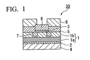
- FIG. 1 is a schematic cross-sectional view illustrating a Schottky barrier diode as one embodiment and to which the invention is applied.
- a Schottky barrier diode 30 is schematically composed of a silicon carbide (SiC) substrate 1, an ohmic electrode (electrode having an ohmic property) 2 provided on one surface of the SiC substrate 1, and a Schottky electrode (electrode having a Schottky property) 3 provided on the other surface of the SiC substrate 1.
- the SiC substrate 1 is composed of an n + -type SiC semiconductor substrate 1a, and an n - -type SiC semiconductor layer 1b epitaxially grown on the n + -type SiC semiconductor substrate 1a.
- the n + -type SiC semiconductor substrate 1a is an n-type 4H-SiC substrate, and is for example a substrate having a thickness of 200 to 400 ⁇ m in which nitrogen of 1.0 ⁇ 10 18 to 1.0 ⁇ 10 19 cm -3 is doped.
- the n - -type SiC semiconductor layer 1b is, for example, an epitaxial growth layer having a thickness of 4 to 10 ⁇ m, and is a layer in which nitrogen of 0.5 to 2.0 ⁇ 10 16 cm -3 is doped.
- the ohmic electrode 2 is provided on the bottom of the SiC substrate 1, that is, the surface of the n + -type SiC semiconductor substrate 1a on the side opposite to the n - -type SiC semiconductor layer 1b.
- An electrode pad 4 serving as a cathode electrode is provided on the bottom of the ohmic electrode 2 (that is, the surface on the side opposite to the n + -type SiC semiconductor substrate 1a).
- a material of the ohmic electrode 2 is not particularly limited insofar as an ohmic junction to the n + -type SiC semiconductor substrate 1a is formed, the material preferably contains, for example, nickel (Ni) or nickel/titanium (Ni/Ti) and the like.
- the thickness of the ohmic electrode 2 is preferably in the range of 20 to 1,000 nm, more preferably in the range of 50 to 200 nm, and particularly preferably in the range of 90 to 110 nm. When the thickness thereof is less than 20 nm, it is not preferable because the electrode becomes non-ohmic. In addition, when the thickness thereof exceeds 1,000 nm, it is not preferable because characteristic deterioration occurs due to an increase in carbon precipitation.
- a material of the electrode pad 4 is not particularly limited, it is possible to use, for example, titanium/nickel/silver (Ti/Ni/Ag) and the like.
- the thickness of the electrode pad 4 is preferably in the range of 200 to 700 nm.
- the upper surface of the SiC substrate 1, that is, the surface of the n - -type SiC semiconductor layer 1b on the side opposite to the n + -type SiC semiconductor substrate 1a is coated by a silicon oxide film 5 having a thickness of a few ⁇ m or so.
- An opening is provided in a portion of the silicon oxide film 5, and the Schottky electrode 3 is provided on the surface of the n - -type SiC semiconductor layer 1b exposed from this opening.
- An electrode pad 6 serving as an anode electrode is provided on the upper surface of the Schottky electrode 3.
- a material of the Schottky electrode 3 is not particularly limited insofar as it is a metal having a large barrier to the n - -type SiC semiconductor layer 1b, it is possible to use, for example, molybdenum (Mo), titanium (Ti), nickel (Ni) and the like. In the embodiment, it is particularly preferable to use molybdenum (Mo) because of stability even at high temperature.
- the thickness of the Schottky electrode 3 is preferably in the range of 10 to 1,000 nm, more preferably in the range of 50 to 500 nm, and particularly preferably in the range of 90 to 110 nm. When the thickness thereof is less than 10 nm, it is not preferable because of the unstable characteristics thereof. In addition, when the thickness thereof exceed 1,000 nm, it is not preferable because of peel-off due to stress.
- a material of the electrode pad 6 is not particularly limited, it is possible to use, for example, nickel/titanium/aluminum (Ni/Ti/Al) and the like.
- the thickness of the electrode pad 6 is preferably in the range of 2,000 to 7,000 nm.
- a p-type region 7 of a low-impurity concentration as a JTE (Junction Termination Extension) structure is provided in the surface of the n - -type semiconductor layer 1b on the side opposite to the n + -type SiC semiconductor substrate 1a.
- the p-type region 7 is provided in the periphery of the Schottky electrode 3 so as to partially overlap the Schottky electrode 3.
- the p-type region 7 for example, aluminum (Al) is implanted.
- the Al concentration is preferably, for example, 1.0 ⁇ 10 17 to 1.0 ⁇ 10 19 cm -3 .
- the thickness of the p-type region 7 is preferably 0.1 to 1.0 ⁇ m.
- the upper surface of the silicon oxide film 5 is coated by a protective layer 8 made of polyimide and the like.
- An opening is provided in a portion of the protective layer 8, and the upper surface of electrode pad 6 is exposed from this opening.
- the central region surrounded by the p-type region 7 is an active region as a Schottky diode.
- the Schottky barrier diode 30 according to the embodiment can be manufactured by, for example, the following method.
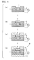
- (a) to (d) of FIG. 2, (a) to (d) of FIG. 3 and (a) to (d) of FIG. 4 are process cross-sectional views illustrating methods of manufacturing the Schottky barrier diode 30 according to the embodiment.
- the SiC substrate 1 is obtained by epitaxially growing the n - -type semiconductor layer 1b on the surface (here, Si surface) of the n + -type SiC semiconductor substrate 1a.
- a CVD method can be used in the formation of the n - -type semiconductor layer 1b.
- process conditions for example, silane and propane which are raw material gases and nitrogen which is a dopant gas are supplied to a chamber under a reduced-pressure atmosphere of 10 -6 Pa or less at a growth temperature of 1600°C. In this way, the n - -type semiconductor layer 1b having a thickness of 8 ⁇ m and an impurity concentration of 1 ⁇ 10 16 cm -3 is formed.
- the n - -type semiconductor layer 1b becomes an active layer forming an active region of the Schottky diode 30, and has a function of securing an off withstanding voltage of the Schottky diode 30.
- the thickness of the n - -type semiconductor layer 1b is set to 4 to 10 ⁇ m, and the impurity concentration thereof is set to 0.5 ⁇ 10 16 to 2.0 ⁇ 10 16 cm -3 .
- a mask layer 11 made of an oxide film is formed on the surface of the n - -type semiconductor layer 1b.
- an oxide film is formed on the surface of the n - -type semiconductor layer 1b by a CVD method and the like.
- the mask layer 11 made of an oxide film having a thickness of 2.0 ⁇ m is formed on the surface of the n - -type semiconductor layer 1b.
- an opening 11a is formed by patterning the mask layer 11.
- the opening 11a is formed so that the surface of the n - -type semiconductor layer 1b for forming the p-type region 7 is exposed.
- an impurity for forming the p-type region 7 on the surface of the n - -type semiconductor layer 1b exposed from the opening 11a of the mask layer 11, for example, aluminum (Al) is implanted at an acceleration voltage of 10 to 300 kV.
- the concentration of implanted A1 is set to, for example, 2.0 ⁇ 10 18 cm -3 . In this way, an impurity implantation layer 12 is formed.
- a method for forming the carbon film 13 is not particularly limited insofar as a carbon film capable of being used as a protective film in which activation heat treatment is performed can be formed.
- a resist is applied on the n - -type semiconductor layer 1b, and then may be heated to form a carbonized film.
- the carbon film 13 may be formed by sputtering or CVD.
- activation heat treatment is performed using the carbon film 13 as a protective film.
- the activation heat treatment is performed, for example, in an argon (Ar) atmosphere or an atmosphere in which the pressure is reduced to 1 ⁇ 10 -2 Pa or less, at a heating temperature of 1,600 to 2,000°C, and during a heating time of 1 to 5 minutes. Thereby, the p-type region 7 is formed.
- the carbon film 13 used as a protective film is removed.
- the carbon film 13 is removed by carbonizing the carbon film by thermal oxidation in an oxygen atmosphere.
- thermal oxidation processing is performed on the surface and the back of the SiC substrate 1, and oxide films 14 and 15 are respectively formed on the surfaces of the n + -type SiC semiconductor substrate 1a and the n - -type semiconductor layer 1b as surface protective films.
- This thermal oxidation processing is performed in a dry oxygen atmosphere at a temperature of 1,200°C for 0.5 hours using a thermal oxidation furnace.
- the oxide film 14 having a thickness of 90 nm or so is formed on the surface of the n + -type SiC semiconductor substrate 1a
- the oxide film 15 having a thickness of 20 nm or so is formed on the surface of the n - -type semiconductor layer 1b.
- the ohmic electrode 2 is formed on one surface of the SiC substrate 1, that is, the surface of the n + -type SiC semiconductor substrate 1a.
- the ohmic electrode 2 can be formed by, for example, the following method. First, the oxide film 14 formed on the surface of the n + -type SiC semiconductor substrate 1a is removed, and the n + -type SiC semiconductor substrate 1a is exposed. The oxide film 14 can be removed by performing etching using hydrofluoric acid. Next, a film (having a thickness of 200 nm or so) made of, for example, nickel is formed on the exposed n + -type SiC semiconductor substrate 1a as an electrode material (first electrode material) by a vacuum vapor deposition method or a sputtering method.
- annealing is performed in an inert atmosphere of argon or the like, at a temperature range of 930 to 950°C for 1 to 10 minutes.
- nickel reacts with Si in the n + -type SiC semiconductor substrate 1a to form nickel silicide.
- the ohmic electrode 2 is formed. Since the nickel silicide is formed in the interface between the ohmic electrode 2 and the n + -type SiC semiconductor substrate 1a, good ohmic characteristics can be realized.
- an oxide film is further deposited on the surface of the oxide film 15 formed on the surface of the n - -type semiconductor layer 1b using a CVD method and the like to thereby form the silicon oxide film 5.
- a portion of the silicon oxide film 5 is removed, and a Schottky electrode 3 contacting the other surface of the SiC substrate 1, that is, the surface of the n - -type semiconductor layer 1b is formed.
- the Schottky electrode 3 is provided in a region surrounded by the p-type region 7 in the surface of the n - -type semiconductor layer 1b so as to contact the inner edge in the surface of the p-type region 7.
- the Schottky electrode 3 can be formed by, for example, the following method. First, a resist layer which is not shown in the drawing is formed on a predetermined region in the silicon oxide film 5 by well-known photolithography. Thereafter, wet etching is performed using hydrofluoric acid as an etching solution, and the portion which is not covered by a resist layer in the silicon oxide film 5 is removed. Thereby, the surface of the n - -type semiconductor layer 1b is exposed.
- an electrode material film (having a thickness of 100 nm or so) made of, for example, molybdenum (Mo) as a second electrode material is formed on the exposed surface of the n - -type semiconductor layer 1b and the resist layer by a vacuum vapor deposition method or a sputtering method. Thereafter, a molybdenum film is patterned (lift-off method) by removing the resist layer, and the Schottky electrode 3 is formed.
- Mo molybdenum
- the resist layer is removed, and then annealing is performed in an inert atmosphere of argon and the like, at a temperature of 600 to 700°C for approximately 30 minutes.
- the above-mentioned heat treatment for stabilization of the Schottky junction is performed at a temperature lower than the annealing temperature of the ohmic electrode 2.
- this process is performed after attainment of the annealing temperature of the ohmic electrode 2.
- the electrode pad 6 is formed on the surface of the Schottky electrode 3.
- an insulating material such as a silicon oxide is deposited using a CVD method so as to cover the Schottky electrode 3.
- the electrode pad 6 is provided inside the contact hole.
- the electrode pad 6 can be formed by depositing a conductive material such as, for example, nickel/titanium/aluminum (Ni/Ti/Al) inside the contact hole to form a conductive film (having a thickness of, for example, 3 ⁇ m), and patterning this conductive film using a well-known photolithography technique and an etching technique.
- a conductive material such as, for example, nickel/titanium/aluminum (Ni/Ti/Al) inside the contact hole to form a conductive film (having a thickness of, for example, 3 ⁇ m), and patterning this conductive film using a well-known photolithography technique and an etching technique.
- the protective layer 8 is formed on the surfaces of the silicon oxide film 5 and the electrode pad 6.
- a layer made of an insulating material such as polyimide is formed so as to cover the surfaces of the silicon oxide film 5 and the electrode pad 6.
- an opening is formed in a portion of the protective layer 8 by patterning the layer using a well-known photolithography technique and an etching technique, and the upper surface of the electrode pad 6 is exposed from this opening.
- the electrode pad 4 is formed on the surface of the ohmic electrode 2.
- the electrode pad 4 is formed by depositing a conductive material such as titanium/nickel/silver (Ti/Ni/Ag) on the surface of the ohmic electrode 2. In this way, the Schottky barrier diode 30 is obtained.
- the configuration is made such that the temperature range of the heat treatment at the time of forming the ohmic electrode 2 on one surface of the SiC substrate 1, that is, the surface of the n + -type SiC semiconductor substrate 1a is limited to 930 to 950°C.
- the Schottky barrier diode 30 having a high forward current and a low reverse leakage current is obtained by forming the Schottky electrode 3 on the other surface of the SiC substrate 1, that is, the surface of the n - -type semiconductor layer 1b.
- the Schottky barrier diode 30 having a high forward current and a low reverse leakage current by a simple method in which the heat treatment temperature is set to the optimum temperature range.
- the technical scope of the invention is not limited to the above-mentioned embodiment, but various modifications can be added without departing from the gist of the invention.
- the n - -type semiconductor layer 1b is epitaxially grown on the Si surface in the n + -type SiC semiconductor substrate 1a
- the Schottky diode may be formed by epitaxially growing the n - -type semiconductor layer 1b on the C surface.
- the silicon oxide film 5 thermal oxide film, CVD oxide film
- polyimide may be formed directly on the semiconductor surface without using this.
- this method can be similarly applied to FETs or integrated devices including a Schottky barrier in the components without being limited to the single Schottky barrier diode.
- a Schottky barrier diode of the example was manufactured by the following procedure. First, as a SiC semiconductor, an n-type 4H-SiC semiconductor layer was prepared which was epitaxially grown to a thickness of 8 ⁇ m and at a carrier concentration of 1 ⁇ 10 16 cm -3 , on an n-type 4H-SiC semiconductor substrate (its thickness was 350 ⁇ m and its resistivity was 0.02 ⁇ cm) having a diameter of 3 inches.
- the surface of the above-mentioned SiC semiconductor was cleaned, and then was heated in an oxygen atmosphere at 1,200°C for 2 hours, to form a thermal oxide film.
- a resist film was applied to the n-type 4H-SiC semiconductor epitaxial layer side, and the thermal oxide film on the 4H-SiC semiconductor substrate side was removed by immersion in HF for 10 minutes.
- the resist film was removed by immersion in an organic solvent. In this way, the thermal oxide film was formed only on the n-type 4H-SiC semiconductor epitaxial layer side.
- the above-mentioned SiC semiconductor was put into a vapor deposition apparatus, and nickel (Ni) was evaporated on the 4H-SiC semiconductor substrate side so as to have a thickness of 100 nm. Then, the semiconductor was put into a chamber and was heated in an argon (Ar) atmosphere at 950°C for 3 minutes, to perform heat treatment. In this way, the nickel was silicified, and an ohmic electrode having good contact resistance was formed.
- the SiC semiconductor was immersed in HF to remove the thermal oxide film on the n-type 4H-SiC semiconductor epitaxial layer side, and a resist pattern was formed on the surface at the n-type 4H-SiC semiconductor epitaxial layer side so that a Schottky electrode was formed to 2 square mm using a photolithography technique.
- the SiC semiconductor was put into the vapor deposition apparatus, and molybdenum (Mo) was formed on the surface at the epitaxial layer side of the n-type 4H-SiC semiconductor layer, to create a pattern of the Schottky electrode by performing lift-off in an organic solvent.
- the semiconductor was put into the chamber, to perform heat treatment in an argon (Ar) atmosphere at 650°C for 10 minutes. In this way, a molybdenum (Mo) electrode having Schottky characteristics was formed.
- the leakage current at the time of applying a reverse voltage of 300 V was 1 ⁇ 10 -6 A or less.
- the forward current at the time of applying a forward voltage of 1.65 V was 500 A/cm 2 . From the above, it was confirmed that the silicon carbide semiconductor device of the invention had both of the low leakage current and the high forward current (low forward voltage) to a high degree.
- a Schottky barrier diode of the example was manufactured by the following procedure. First, as a SiC semiconductor, an n-type 4H-SiC semiconductor layer was prepared which was epitaxially grown to a thickness of 8 ⁇ m and at a carrier concentration of 1 ⁇ 10 16 cm -3 , on an n-type 4H-SiC semiconductor substrate (its thickness was 350 ⁇ m and its resistivity was 0.02 ⁇ cm) having a diameter of 3 inches.
- the surface of the above-mentioned SiC semiconductor was cleaned, and then was heated in an oxygen atmosphere at 1,200°C for 2 hours, to form a thermal oxide film.
- a resist film was applied to the n-type 4H-SiC semiconductor epitaxial layer side, and the thermal oxide film on the 4H-SiC semiconductor substrate side was removed by immersion in HF for 10 minutes.
- the resist film was removed by immersion in an organic solvent. In this way, the thermal oxide film was formed only on the n-type 4H-SiC semiconductor epitaxial layer side.
- the above-mentioned SiC semiconductor was put into a vapor deposition apparatus, and nickel (Ni) was evaporated on the 4H-SiC semiconductor substrate side so as to have a thickness of 100 nm. Then, the semiconductor was put into a chamber and was heated in an argon (Ar) atmosphere at 930°C for 3 minutes, to perform heat treatment. In this way, the nickel was silicified, and an ohmic electrode having good contact resistance was formed.
- the SiC semiconductor was immersed in HF to remove the thermal oxide film on the n-type 4H-SiC semiconductor epitaxial layer side, and a resist pattern was formed on the surface at the n-type 4H-SiC semiconductor epitaxial layer side so that a Schottky electrode was formed to 2 square mm using a photolithography technique.
- the SiC semiconductor was put into the vapor deposition apparatus, and molybdenum (Mo) was formed on the surface at the epitaxial layer side of the n-type 4H-SiC semiconductor layer, to create a pattern of the Schottky electrode by performing lift-off in an organic solvent.
- the semiconductor was put into the chamber, to perform heat treatment in an argon (Ar) atmosphere at 650°C for 10 minutes. In this way, a molybdenum (Mo) electrode having Schottky characteristics was formed.
- the leakage current at the time of applying a reverse voltage of 300 V was 1 ⁇ 10 -6 A or less.
- the forward current at the time of applying a forward voltage of 1.65 V was 500 A/cm 2 . From the above, it was confirmed that the silicon carbide semiconductor device of the invention had both of the low leakage current and the high forward current to a high degree.
- a Schottky barrier diode of the example was manufactured by the following procedure. First, as a SiC semiconductor, an n-type 4H-SiC semiconductor layer was prepared which was epitaxially grown to a thickness of 8 ⁇ m and at a carrier concentration of 1 ⁇ 10 16 cm -3 , on an n-type 4H-SiC semiconductor substrate (its thickness was 350 ⁇ m and its resistivity was 0.02 ⁇ cm) having a diameter of 3 inches.
- the surface of the above-mentioned SiC semiconductor was cleaned, and then was heated in an oxygen atmosphere at 1,200°C for 2 hours, to form a thermal oxide film.
- a resist film was applied to the n-type 4H-SiC semiconductor epitaxial layer side, and the thermal oxide film on the 4H-SiC semiconductor substrate side was removed by immersion in HF for 10 minutes.
- the resist film was removed by immersion in an organic solvent. In this way, the thermal oxide film was formed only on the n-type 4H-SiC semiconductor epitaxial layer side.
- the above-mentioned SiC semiconductor was put into a vapor deposition apparatus, and nickel (Ni) was evaporated on the 4H-SiC semiconductor substrate side so as to have a thickness of 100 nm. Then, the semiconductor was put into a chamber and was heated in an argon (Ar) atmosphere at 970°C for 3 minutes, to perform heat treatment. In this way, the nickel was silicified, and an ohmic electrode having good contact resistance was formed.
- the SiC semiconductor was immersed in HF to remove the thermal oxide film on the n-type 4H-SiC semiconductor epitaxial layer side, and a resist pattern was formed on the surface at the n-type 4H-SiC semiconductor epitaxial layer side so that a Schottky electrode was formed to 2 square mm using a photolithography technique.
- the SiC semiconductor was put into the vapor deposition apparatus, and molybdenum (Mo) was formed on the surface at the epitaxial layer side of the n-type 4H-SiC semiconductor layer, to create a pattern of the Schottky electrode by performing lift-off in an organic solvent.
- the semiconductor was put into the chamber, to perform heat treatment in an argon (Ar) atmosphere at 650°C for 10 minutes. In this way, a molybdenum (Mo) electrode having Schottky characteristics was formed.
- the leakage current at the time of applying a reverse voltage of 300 V was 1 ⁇ 10 -7 A or more, and it was confirmed that the leakage current became high with respect to the heat treatment temperature of the ohmic electrode of 950°C or lower.
- a Schottky barrier diode of the example was manufactured by the following procedure. First, as a SiC semiconductor, an n-type 4H-SiC semiconductor layer was prepared which was epitaxially grown to a thickness of 8 ⁇ m and at a carrier concentration of 1 ⁇ 10 16 cm -3 , on an n-type 4H-SiC semiconductor substrate (its thickness was 350 ⁇ m and its resistivity was 0.02 ⁇ cm) having a diameter of 3 inches.
- the surface of the above-mentioned SiC semiconductor was cleaned, and then was heated in an oxygen atmosphere at 1,200°C for 2 hours, to form a thermal oxide film.
- a resist film was applied to the n-type 4H-SiC semiconductor epitaxial layer side, and the thermal oxide film on the 4H-SiC semiconductor substrate side was removed by immersion in HF for 10 minutes.
- the resist film was removed by immersion in an organic solvent. In this way, the thermal oxide film was formed only on the n-type 4H-SiC semiconductor epitaxial layer side.
- the above-mentioned SiC semiconductor was put into a vapor deposition apparatus, and nickel (Ni) was evaporated on the 4H-SiC semiconductor substrate side so as to have a thickness of 100 nm. Then, the semiconductor was put into a chamber and was heated in an argon (Ar) atmosphere at 900°C for 3 minutes, to perform heat treatment. In this way, the nickel was silicified, and an ohmic electrode having good contact resistance was formed.
- the SiC semiconductor was immersed in HF to remove the thermal oxide film on the n-type 4H-SiC semiconductor epitaxial layer side, and a resist pattern was formed on the surface at the n-type 4H-SiC semiconductor epitaxial layer side so that a Schottky electrode was formed to 2 square mm using a photolithography technique.
- the SiC semiconductor was put into the vapor deposition apparatus, and molybdenum (Mo) was formed on the surface at the epitaxial layer side of the n-type 4H-SiC semiconductor layer, to create a pattern of the Schottky electrode by performing lift-off in an organic solvent.
- the semiconductor was put into the chamber, to perform heat treatment in an argon (Ar) atmosphere at 650°C for 10 minutes. In this way, a molybdenum (Mo) electrode having Schottky characteristics was formed.
- the forward voltage in the forward current of 500 A/cm 2 was 1.75 V or more, and it was confirmed that the forward voltage became high with respect to the heat treatment temperature of the ohmic electrode of 930°C or higher.
- the influence of the annealing temperature at the time of forming the ohmic electrode was confirmed using the Schottky barrier diode obtained in the above-mentioned examples and comparative examples.
- the size of the Schottky electrode was 2 square mm.
- FIG. 5 is a diagram illustrating the relationship between the heat treatment temperature at the time of forming the ohmic electrode and the reverse leakage current.
- the reverse leakage current in the reverse applied voltage of 300 V increased when the annealing temperature at the time of forming the ohmic electrode was higher than the specific temperature. That is, when the reverse leakage current value of 1 ⁇ 10 6 A in the reverse applied voltage of 300 V, which is generally required, was used as a reference, it was known that the annealing temperature at the time of forming the ohmic electrode 2 was achieved at 950°C or lower.
- FIG. 6 is a diagram illustrating the relationship between the heat treatment temperature at the time of forming the ohmic electrode and the forward voltage.
- the forward voltage at the time of causing the amount of 500 A/cm 2 to flow decreases due to a decrease in the contact resistance of the ohmic electrode. Therefore, it was known that the case where the forward voltage is stabilized and becomes a voltage of 1.65 V which is a target value was achieved at the annealing temperature of 930°C or higher.
- the heat treatment temperature at the time of forming the ohmic electrode showed an optimum range at a temperature of 930°C to 950°C. It was confirmed that the Schottky barrier diode was obtained which has characteristics that the resistance value at the time of causing the forward current to flow is small and the leakage current at the time of applying the reverse voltage is low, by setting the heat treatment temperature to the optimum range.
- the annealing temperature at the time of forming the ohmic electrode influenced the reverse leakage current from the comparative experiment in which the formation of the ohmic electrode was performed after the formation of the Schottky electrode and annealing was not performed.
- the reverse leakage current is stabilized in a low level.
- the contact resistance of the ohmic electrode was large, and thus it was known that the conditions could not be adopted as preparation conditions of the practical Schottky barrier diode.
- the invention can be applied to a method for manufacturing a silicon carbide semiconductor device.
Landscapes
- Electrodes Of Semiconductors (AREA)
Abstract
Provided is a method for manufacturing a silicon carbide semiconductor device which is capable of obtaining the silicon carbide semiconductor device having a high forward current and a low reverse leakage current by a simple method. The method for manufacturing a silicon carbide semiconductor device includes the steps of: forming a film made of a first electrode material on one surface of a silicon carbide substrate, and forming an ohmic electrode by performing heat treatment at a temperature range of 930 to 950°C; and forming a film made of a second electrode material on the other surface of the silicon carbide substrate, and forming a Schottky electrode by performing heat treatment.
Description
- The present invention relates to a method for manufacturing a silicon carbide semiconductor device.
Priority is claimed on Japanese Patent Application No.2008-333659, filed December 26, 2008 - Silicon carbide semiconductors have excellent characteristics with a larger dielectric breakdown voltage, a wider energy bandgap and a higher thermal conductivity than silicon semiconductors. Therefore, silicon carbide semiconductors are expected to be applied to light-emitting devices, high-power devices, high-temperature-tolerant devices, radiation-proof devices, high-frequency devices and the like.
- Incidentally, as devices (SiC semiconductor devices) in which the above-mentioned silicon carbide semiconductor is used, Schottky barrier diodes are known. The Schottky barrier diode is a diode in which rectification (Schottky effect) generated in the junction surface between a metal and a semiconductor is used, and has characteristics such that the forward drop voltage is lower than that of a PN diode, and the reverse recovery time is shorter than this. Therefore, the Schottky barrier diode is often used in a power supply circuit such as a switching regulator that performs high-frequency switching.
- However, the Schottky barrier diode has a drawback in that the reverse leakage current is larger than that of the PN diode, and the reverse withstand voltage is lower than this. Therefore, in the Schottky barrier diode in which a SiC semiconductor device is used, there has been a problem in that an ohmic electrode which has a low contact resistance is formed in order to increase the forward current, and the reverse leakage current is reduced.
- Generally, in order to obtain an ohmic electrode which has a low contact resistance, it is known that nickel (Ni) may be used as an electrode (see, for example,
PTLs 1 or 2). In addition, it is known that after Ni is formed on the surface of a SiC substrate, heat treatment thereof at high temperature is effective in obtaining an ohmic electrode which has a low contact resistance. - On the other hand, various investigations have been made in order to reduce the reverse leakage current. For example, reduction in crystal defects of a micropipe or the like existing in a substrate or an epitaxial layer, a guard ring structure for preventing field effect concentration of the Schottky electrode end, and the like are proposed. Further, the impurity concentration of a SiC layer at the Schottky electrode side, or the height of the Schottky electrode, and the like have been investigated (see
PTLs 3 to 5). -
- [PTL 1] Japanese Unexamined Patent Application Publication No.
2003-243323 - [PTL 2] Japanese Unexamined Patent Application Publication No.
2007-184571 - [PTL 3] Japanese Unexamined Patent Application Publication No.
2000-133819 - [PTL 4] Japanese Unexamined Patent Application Publication No.
2004-266115 - [PTL 5] Japanese Unexamined Patent Application Publication No.
2007-149839 - However, the investigations for reducing the conventional leakage current disclosed in
PTLs 3 to 5 seek a solution to the cause of the leakage current in a substrate, crystallization of an epitaxial layer, a structure and preparation conditions of the surface side at which the Schottky electrode exists, and the like. Since processes become complicated using any of the above methods, there has been a problem in that it is difficult to stably produce the Schottky barrier diode in which the leakage current is reduced. - The invention is contrived in view of such circumstances, and an object thereof is to provide a method for manufacturing a silicon carbide semiconductor device which is capable of obtaining a silicon carbide semiconductor device having a low forward voltage and a low reverse leakage current by a simple method.
- The inventor has examined a method for suppressing the leakage current of the SiC semiconductor device (Schottky barrier diode), and has elucidated that the reverse leakage current increases when the heat treatment temperature of an ohmic electrode (Ni) is increased in order to obtain an ohmic electrode of a low contact resistance.
The inventor has found that a SiC semiconductor device is obtained which has characteristics such that the resistance value at the time of causing the forward current to flow is small and the leakage current at the time of applying a reverse voltage is low, by setting the heat treatment temperature at the time of forming the ohmic electrode to an optimum range, and has completed the invention. - That is, the invention relates to the following:
- (1) A method for manufacturing a silicon carbide semiconductor device, including the steps of: forming a film made of a first electrode material on one surface of ba silicon carbide substrate, and forming an ohmic electrode by performing heat treatment at a temperature range of 930 to 950°C; and forming a film made of a second electrode material on the other surface of the silicon carbide substrate, and forming a Schottky electrode by performing heat treatment.
- (2) The method for manufacturing a silicon carbide semiconductor device according to the above (1), wherein the first electrode material includes at least nickel.
- (3) The method for manufacturing a silicon carbide semiconductor device according to the above (1) or (2), wherein the second electrode material is molybdenum.
- (4) The method for manufacturing a silicon carbide semiconductor device according to any one of the above (1) to (3), wherein the heat treatment temperature in the step of forming the Schottky electrode is in the range of 600 to 700°C.
- (5) The method for manufacturing a silicon carbide semiconductor device according to any one of the above (1) to (4), wherein the silicon carbide semiconductor device is a Schottky barrier diode.
- According to the method for manufacturing a silicon carbide semiconductor device of the invention, the configuration is made such that the temperature range of the heat treatment at the time of forming the ohmic electrode on one surface of the silicon carbide substrate is limited to 930 to 950°C. The silicon carbide semiconductor device having a high forward current and a low reverse leakage current is obtained by forming the Schottky electrode on the other surface of the above-mentioned silicon carbide substrate. That is, when the ohmic electrode is formed on the surface of the silicon carbide substrate on the opposite side to which the Schottky electrode is formed, it is possible to manufacture the silicon carbide semiconductor device having a high forward current and a low reverse leakage current by a simple method in which the heat treatment temperature is set to the optimum temperature range.
-
-
FIG. 1 is a schematic cross-sectional view illustrating a Schottky barrier diode as one embodiment and to which the invention is applied. -
FIG. 2 is a process cross-sectional view illustrating a method for manufacturing the Schottky barrier diode according to the embodiment. -
FIG. 3 is a process cross-sectional view illustrating the method for manufacturing the Schottky barrier diode according to the embodiment. -
FIG. 4 is a process cross-sectional view illustrating the method for manufacturing the Schottky barrier diode according to the embodiment. -
FIG. 5 is a diagram explaining examples, and a diagram illustrating the relationship between the heat treatment temperature at the time of forming an ohmic electrode and the reverse leakage current. -
FIG. 6 is a diagram explaining the examples, and a diagram illustrating the relationship between the heat treatment temperature at the time of forming the ohmic electrode and the forward voltage. - Hereinafter, reference will be made to the drawings to give a detailed description of a method for manufacturing a silicon carbide semiconductor device as one embodiment and to which the invention is applied. Here, as one of the silicon carbide semiconductor devices, description will be made using a Schottky barrier diode. In the drawings used in the following description, the featured portions of the invention may be enlarged, for convenience, in order to make the features thereof easier to understand, and the dimension ratios and the like for each of the components are not limited to the same dimensions as in reality.
-
FIG. 1 is a schematic cross-sectional view illustrating a Schottky barrier diode as one embodiment and to which the invention is applied. As shown inFIG. 1 , aSchottky barrier diode 30 is schematically composed of a silicon carbide (SiC)substrate 1, an ohmic electrode (electrode having an ohmic property) 2 provided on one surface of theSiC substrate 1, and a Schottky electrode (electrode having a Schottky property) 3 provided on the other surface of theSiC substrate 1. In particular, theSiC substrate 1 is composed of an n+-typeSiC semiconductor substrate 1a, and an n--typeSiC semiconductor layer 1b epitaxially grown on the n+-typeSiC semiconductor substrate 1a. - The n+-type
SiC semiconductor substrate 1a is an n-type 4H-SiC substrate, and is for example a substrate having a thickness of 200 to 400 µm in which nitrogen of 1.0×10¹⁸ to 1.0×1019 cm-3 is doped. In addition, the n--typeSiC semiconductor layer 1b is, for example, an epitaxial growth layer having a thickness of 4 to 10 µm, and is a layer in which nitrogen of 0.5 to 2.0×1016 cm-3 is doped. - The
ohmic electrode 2 is provided on the bottom of theSiC substrate 1, that is, the surface of the n+-typeSiC semiconductor substrate 1a on the side opposite to the n--typeSiC semiconductor layer 1b. Anelectrode pad 4 serving as a cathode electrode is provided on the bottom of the ohmic electrode 2 (that is, the surface on the side opposite to the n+-typeSiC semiconductor substrate 1a). - Although a material of the ohmic electrode 2 (first electrode material) is not particularly limited insofar as an ohmic junction to the n+-type
SiC semiconductor substrate 1a is formed, the material preferably contains, for example, nickel (Ni) or nickel/titanium (Ni/Ti) and the like. In addition, the thickness of theohmic electrode 2 is preferably in the range of 20 to 1,000 nm, more preferably in the range of 50 to 200 nm, and particularly preferably in the range of 90 to 110 nm. When the thickness thereof is less than 20 nm, it is not preferable because the electrode becomes non-ohmic. In addition, when the thickness thereof exceeds 1,000 nm, it is not preferable because characteristic deterioration occurs due to an increase in carbon precipitation. - Although a material of the
electrode pad 4 is not particularly limited, it is possible to use, for example, titanium/nickel/silver (Ti/Ni/Ag) and the like. In addition, the thickness of theelectrode pad 4 is preferably in the range of 200 to 700 nm. - The upper surface of the
SiC substrate 1, that is, the surface of the n--typeSiC semiconductor layer 1b on the side opposite to the n+-typeSiC semiconductor substrate 1a is coated by asilicon oxide film 5 having a thickness of a few µm or so. An opening is provided in a portion of thesilicon oxide film 5, and the Schottkyelectrode 3 is provided on the surface of the n--typeSiC semiconductor layer 1b exposed from this opening. Anelectrode pad 6 serving as an anode electrode is provided on the upper surface of the Schottkyelectrode 3. - Although a material of the Schottky electrode 3 (second electrode material) is not particularly limited insofar as it is a metal having a large barrier to the n--type
SiC semiconductor layer 1b, it is possible to use, for example, molybdenum (Mo), titanium (Ti), nickel (Ni) and the like. In the embodiment, it is particularly preferable to use molybdenum (Mo) because of stability even at high temperature. In addition, the thickness of theSchottky electrode 3 is preferably in the range of 10 to 1,000 nm, more preferably in the range of 50 to 500 nm, and particularly preferably in the range of 90 to 110 nm. When the thickness thereof is less than 10 nm, it is not preferable because of the unstable characteristics thereof. In addition, when the thickness thereof exceed 1,000 nm, it is not preferable because of peel-off due to stress. - Although a material of the
electrode pad 6 is not particularly limited, it is possible to use, for example, nickel/titanium/aluminum (Ni/Ti/Al) and the like. In addition, the thickness of theelectrode pad 6 is preferably in the range of 2,000 to 7,000 nm. - In addition, a p-
type region 7 of a low-impurity concentration as a JTE (Junction Termination Extension) structure is provided in the surface of the n--type semiconductor layer 1b on the side opposite to the n+-typeSiC semiconductor substrate 1a. The p-type region 7 is provided in the periphery of theSchottky electrode 3 so as to partially overlap theSchottky electrode 3. - In the p-
type region 7, for example, aluminum (Al) is implanted. The Al concentration is preferably, for example, 1.0×10¹⁷ to 1.0×1019 cm-3. In addition, the thickness of the p-type region 7 is preferably 0.1 to 1.0 µm. - The upper surface of the
silicon oxide film 5 is coated by aprotective layer 8 made of polyimide and the like. An opening is provided in a portion of theprotective layer 8, and the upper surface ofelectrode pad 6 is exposed from this opening.
The central region surrounded by the p-type region 7 is an active region as a Schottky diode. - Next, a description will be made of a method for manufacturing the
Schottky barrier diode 30 according to the embodiment.
TheSchottky barrier diode 30 according to the embodiment can be manufactured by, for example, the following method. (a) to (d) ofFIG. 2, (a) to (d) ofFIG. 3 and(a) to (d) of FIG. 4 are process cross-sectional views illustrating methods of manufacturing theSchottky barrier diode 30 according to the embodiment. - First, as shown in (a) of
FIG. 2 , theSiC substrate 1 is obtained by epitaxially growing the n--type semiconductor layer 1b on the surface (here, Si surface) of the n+-typeSiC semiconductor substrate 1a.
A CVD method can be used in the formation of the n--type semiconductor layer 1b. As process conditions, for example, silane and propane which are raw material gases and nitrogen which is a dopant gas are supplied to a chamber under a reduced-pressure atmosphere of 10-6 Pa or less at a growth temperature of 1600°C. In this way, the n--type semiconductor layer 1b having a thickness of 8 µm and an impurity concentration of 1 ×1016 cm-3 is formed. - The n--
type semiconductor layer 1b becomes an active layer forming an active region of theSchottky diode 30, and has a function of securing an off withstanding voltage of theSchottky diode 30. For example, when a Schottky diode having a withstanding voltage of 1.65 V is created, the thickness of the n--type semiconductor layer 1b is set to 4 to 10 µm, and the impurity concentration thereof is set to 0.5×10¹⁶ to 2.0 × 1016 cm-3. - Next, as shown in (a) of
FIG. 2 , amask layer 11 made of an oxide film is formed on the surface of the n--type semiconductor layer 1b. In particular, an oxide film is formed on the surface of the n--type semiconductor layer 1b by a CVD method and the like. In the embodiment, themask layer 11 made of an oxide film having a thickness of 2.0 µm is formed on the surface of the n--type semiconductor layer 1b. - Next, as shown in (b) of
FIG. 2 , anopening 11a is formed by patterning themask layer 11. Theopening 11a is formed so that the surface of the n--type semiconductor layer 1b for forming the p-type region 7 is exposed. - Next, as shown in (c) of
FIG. 2 , an impurity for forming the p-type region 7 on the surface of the n--type semiconductor layer 1b exposed from theopening 11a of themask layer 11, for example, aluminum (Al) is implanted at an acceleration voltage of 10 to 300 kV. In addition, the concentration of implanted A1 is set to, for example, 2.0×1018 cm-3. In this way, animpurity implantation layer 12 is formed. - Next, as shown in (d) of
FIG. 2 , themask 11 used in the impurity implantation is removed. Subsequently, acarbon film 13 serving as a protective film in which activation heat treatment is performed is formed on the n--type semiconductor layer 1b and theimpurity implantation layer 12. - A method for forming the
carbon film 13 is not particularly limited insofar as a carbon film capable of being used as a protective film in which activation heat treatment is performed can be formed. In particular, for example, a resist is applied on the n--type semiconductor layer 1b, and then may be heated to form a carbonized film. In addition, thecarbon film 13 may be formed by sputtering or CVD. - Next, activation heat treatment is performed using the
carbon film 13 as a protective film. The activation heat treatment is performed, for example, in an argon (Ar) atmosphere or an atmosphere in which the pressure is reduced to 1×10⁻² Pa or less, at a heating temperature of 1,600 to 2,000°C, and during a heating time of 1 to 5 minutes. Thereby, the p-type region 7 is formed. - Next, as shown in (a) of
FIG. 3 , thecarbon film 13 used as a protective film is removed. Thecarbon film 13 is removed by carbonizing the carbon film by thermal oxidation in an oxygen atmosphere. - Next, as shown in (b) of
FIG. 3 , thermal oxidation processing is performed on the surface and the back of theSiC substrate 1, andoxide films SiC semiconductor substrate 1a and the n--type semiconductor layer 1b as surface protective films. This thermal oxidation processing is performed in a dry oxygen atmosphere at a temperature of 1,200°C for 0.5 hours using a thermal oxidation furnace. Thereby, theoxide film 14 having a thickness of 90 nm or so is formed on the surface of the n+-typeSiC semiconductor substrate 1a, and theoxide film 15 having a thickness of 20 nm or so is formed on the surface of the n--type semiconductor layer 1b. - Next, as shown in (c) of
FIG. 3 , theohmic electrode 2 is formed on one surface of theSiC substrate 1, that is, the surface of the n+-typeSiC semiconductor substrate 1a. - The
ohmic electrode 2 can be formed by, for example, the following method. First, theoxide film 14 formed on the surface of the n+-typeSiC semiconductor substrate 1a is removed, and the n+-typeSiC semiconductor substrate 1a is exposed. Theoxide film 14 can be removed by performing etching using hydrofluoric acid. Next, a film (having a thickness of 200 nm or so) made of, for example, nickel is formed on the exposed n+-typeSiC semiconductor substrate 1a as an electrode material (first electrode material) by a vacuum vapor deposition method or a sputtering method. - Subsequently, annealing is performed in an inert atmosphere of argon or the like, at a temperature range of 930 to 950°C for 1 to 10 minutes. Thereby, nickel reacts with Si in the n+-type
SiC semiconductor substrate 1a to form nickel silicide. In this way, theohmic electrode 2 is formed. Since the nickel silicide is formed in the interface between theohmic electrode 2 and the n+-typeSiC semiconductor substrate 1a, good ohmic characteristics can be realized. - Thereafter, as shown in (d) of
FIG. 3 , an oxide film is further deposited on the surface of theoxide film 15 formed on the surface of the n--type semiconductor layer 1b using a CVD method and the like to thereby form thesilicon oxide film 5. - Next, as shown in (a) of
FIG. 4 , a portion of thesilicon oxide film 5 is removed, and aSchottky electrode 3 contacting the other surface of theSiC substrate 1, that is, the surface of the n--type semiconductor layer 1b is formed. TheSchottky electrode 3 is provided in a region surrounded by the p-type region 7 in the surface of the n--type semiconductor layer 1b so as to contact the inner edge in the surface of the p-type region 7. - The
Schottky electrode 3 can be formed by, for example, the following method. First, a resist layer which is not shown in the drawing is formed on a predetermined region in thesilicon oxide film 5 by well-known photolithography. Thereafter, wet etching is performed using hydrofluoric acid as an etching solution, and the portion which is not covered by a resist layer in thesilicon oxide film 5 is removed. Thereby, the surface of the n--type semiconductor layer 1b is exposed. - Subsequently, an electrode material film (having a thickness of 100 nm or so) made of, for example, molybdenum (Mo) as a second electrode material is formed on the exposed surface of the n--
type semiconductor layer 1b and the resist layer by a vacuum vapor deposition method or a sputtering method. Thereafter, a molybdenum film is patterned (lift-off method) by removing the resist layer, and theSchottky electrode 3 is formed. - In the embodiment, in order to strengthen the adhesion between the
Schottky electrode 3 and the n--type semiconductor layer 1b, the resist layer is removed, and then annealing is performed in an inert atmosphere of argon and the like, at a temperature of 600 to 700°C for approximately 30 minutes. The above-mentioned heat treatment for stabilization of the Schottky junction is performed at a temperature lower than the annealing temperature of theohmic electrode 2. In addition, since the temperature of the heat treatment for stabilization of the Schottky junction is lower than the annealing temperature of theohmic electrode 2, this process is performed after attainment of the annealing temperature of theohmic electrode 2. - Next, as shown in (b) of
FIG. 4 , theelectrode pad 6 is formed on the surface of theSchottky electrode 3. First, an insulating material (not shown) such as a silicon oxide is deposited using a CVD method so as to cover theSchottky electrode 3. Next, after a contact hole reaching theSchottky electrode 3 is formed in the insulating material by a well-known dry etching technique, theelectrode pad 6 is provided inside the contact hole. Theelectrode pad 6 can be formed by depositing a conductive material such as, for example, nickel/titanium/aluminum (Ni/Ti/Al) inside the contact hole to form a conductive film (having a thickness of, for example, 3 µm), and patterning this conductive film using a well-known photolithography technique and an etching technique. - Next, as shown in (c) of
FIG. 4 , theprotective layer 8 is formed on the surfaces of thesilicon oxide film 5 and theelectrode pad 6. First, in theprotective layer 8, a layer made of an insulating material such as polyimide is formed so as to cover the surfaces of thesilicon oxide film 5 and theelectrode pad 6. Next, an opening is formed in a portion of theprotective layer 8 by patterning the layer using a well-known photolithography technique and an etching technique, and the upper surface of theelectrode pad 6 is exposed from this opening. - Next, as shown in (d) of
FIG. 4 , theelectrode pad 4 is formed on the surface of theohmic electrode 2.
Theelectrode pad 4 is formed by depositing a conductive material such as titanium/nickel/silver (Ti/Ni/Ag) on the surface of theohmic electrode 2. In this way, theSchottky barrier diode 30 is obtained. - As described above, according to the method for manufacturing the
Schottky barrier diode 30 of the embodiment, the configuration is made such that the temperature range of the heat treatment at the time of forming theohmic electrode 2 on one surface of theSiC substrate 1, that is, the surface of the n+-typeSiC semiconductor substrate 1a is limited to 930 to 950°C. TheSchottky barrier diode 30 having a high forward current and a low reverse leakage current is obtained by forming theSchottky electrode 3 on the other surface of theSiC substrate 1, that is, the surface of the n--type semiconductor layer 1b. As can be seen from the above, when theohmic electrode 2 is formed, it is possible to manufacture theSchottky barrier diode 30 having a high forward current and a low reverse leakage current by a simple method in which the heat treatment temperature is set to the optimum temperature range. - The technical scope of the invention is not limited to the above-mentioned embodiment, but various modifications can be added without departing from the gist of the invention. For example, in the embodiment, although the n--
type semiconductor layer 1b is epitaxially grown on the Si surface in the n+-typeSiC semiconductor substrate 1a, the Schottky diode may be formed by epitaxially growing the n--type semiconductor layer 1b on the C surface. Moreover, in the embodiment, although the silicon oxide film 5 (thermal oxide film, CVD oxide film) is used as a protective film, polyimide may be formed directly on the semiconductor surface without using this. In addition, this method can be similarly applied to FETs or integrated devices including a Schottky barrier in the components without being limited to the single Schottky barrier diode. - Hereinafter, effects of the invention will be specifically described with reference to examples. However, the invention is not limited to these examples.
- A Schottky barrier diode of the example was manufactured by the following procedure.
First, as a SiC semiconductor, an n-type 4H-SiC semiconductor layer was prepared which was epitaxially grown to a thickness of 8 µm and at a carrier concentration of 1 × 1016 cm-3, on an n-type 4H-SiC semiconductor substrate (its thickness was 350 µm and its resistivity was 0.02 Ωcm) having a diameter of 3 inches. - Next, the surface of the above-mentioned SiC semiconductor was cleaned, and then was heated in an oxygen atmosphere at 1,200°C for 2 hours, to form a thermal oxide film. Thereafter, a resist film was applied to the n-type 4H-SiC semiconductor epitaxial layer side, and the thermal oxide film on the 4H-SiC semiconductor substrate side was removed by immersion in HF for 10 minutes. The resist film was removed by immersion in an organic solvent. In this way, the thermal oxide film was formed only on the n-type 4H-SiC semiconductor epitaxial layer side.
- Next, the above-mentioned SiC semiconductor was put into a vapor deposition apparatus, and nickel (Ni) was evaporated on the 4H-SiC semiconductor substrate side so as to have a thickness of 100 nm. Then, the semiconductor was put into a chamber and was heated in an argon (Ar) atmosphere at 950°C for 3 minutes, to perform heat treatment. In this way, the nickel was silicified, and an ohmic electrode having good contact resistance was formed.
- Next, the SiC semiconductor was immersed in HF to remove the thermal oxide film on the n-type 4H-SiC semiconductor epitaxial layer side, and a resist pattern was formed on the surface at the n-type 4H-SiC semiconductor epitaxial layer side so that a Schottky electrode was formed to 2 square mm using a photolithography technique. Then, the SiC semiconductor was put into the vapor deposition apparatus, and molybdenum (Mo) was formed on the surface at the epitaxial layer side of the n-type 4H-SiC semiconductor layer, to create a pattern of the Schottky electrode by performing lift-off in an organic solvent.
- The semiconductor was put into the chamber, to perform heat treatment in an argon (Ar) atmosphere at 650°C for 10 minutes. In this way, a molybdenum (Mo) electrode having Schottky characteristics was formed.
- In the Schottky barrier diode of the example manufactured in this way, the leakage current at the time of applying a reverse voltage of 300 V was 1 × 10⁻⁶ A or less. In addition, the forward current at the time of applying a forward voltage of 1.65 V was 500 A/cm2. From the above, it was confirmed that the silicon carbide semiconductor device of the invention had both of the low leakage current and the high forward current (low forward voltage) to a high degree.
- A Schottky barrier diode of the example was manufactured by the following procedure.
First, as a SiC semiconductor, an n-type 4H-SiC semiconductor layer was prepared which was epitaxially grown to a thickness of 8 µm and at a carrier concentration of 1 × 1016 cm-3, on an n-type 4H-SiC semiconductor substrate (its thickness was 350 µm and its resistivity was 0.02 Ωcm) having a diameter of 3 inches. - Next, the surface of the above-mentioned SiC semiconductor was cleaned, and then was heated in an oxygen atmosphere at 1,200°C for 2 hours, to form a thermal oxide film. Thereafter, a resist film was applied to the n-type 4H-SiC semiconductor epitaxial layer side, and the thermal oxide film on the 4H-SiC semiconductor substrate side was removed by immersion in HF for 10 minutes. The resist film was removed by immersion in an organic solvent. In this way, the thermal oxide film was formed only on the n-type 4H-SiC semiconductor epitaxial layer side.
- Next, the above-mentioned SiC semiconductor was put into a vapor deposition apparatus, and nickel (Ni) was evaporated on the 4H-SiC semiconductor substrate side so as to have a thickness of 100 nm. Then, the semiconductor was put into a chamber and was heated in an argon (Ar) atmosphere at 930°C for 3 minutes, to perform heat treatment. In this way, the nickel was silicified, and an ohmic electrode having good contact resistance was formed.
- Next, the SiC semiconductor was immersed in HF to remove the thermal oxide film on the n-type 4H-SiC semiconductor epitaxial layer side, and a resist pattern was formed on the surface at the n-type 4H-SiC semiconductor epitaxial layer side so that a Schottky electrode was formed to 2 square mm using a photolithography technique. Then, the SiC semiconductor was put into the vapor deposition apparatus, and molybdenum (Mo) was formed on the surface at the epitaxial layer side of the n-type 4H-SiC semiconductor layer, to create a pattern of the Schottky electrode by performing lift-off in an organic solvent.
- The semiconductor was put into the chamber, to perform heat treatment in an argon (Ar) atmosphere at 650°C for 10 minutes. In this way, a molybdenum (Mo) electrode having Schottky characteristics was formed.
- In the Schottky barrier diode of the example manufactured in this way, the leakage current at the time of applying a reverse voltage of 300 V was 1 × 10⁻⁶ A or less. In addition, the forward current at the time of applying a forward voltage of 1.65 V was 500 A/cm2. From the above, it was confirmed that the silicon carbide semiconductor device of the invention had both of the low leakage current and the high forward current to a high degree.
- A Schottky barrier diode of the example was manufactured by the following procedure.
First, as a SiC semiconductor, an n-type 4H-SiC semiconductor layer was prepared which was epitaxially grown to a thickness of 8 µm and at a carrier concentration of 1 × 1016 cm-3, on an n-type 4H-SiC semiconductor substrate (its thickness was 350 µm and its resistivity was 0.02 Ωcm) having a diameter of 3 inches. - Next, the surface of the above-mentioned SiC semiconductor was cleaned, and then was heated in an oxygen atmosphere at 1,200°C for 2 hours, to form a thermal oxide film. Thereafter, a resist film was applied to the n-type 4H-SiC semiconductor epitaxial layer side, and the thermal oxide film on the 4H-SiC semiconductor substrate side was removed by immersion in HF for 10 minutes. The resist film was removed by immersion in an organic solvent. In this way, the thermal oxide film was formed only on the n-type 4H-SiC semiconductor epitaxial layer side.
- Next, the above-mentioned SiC semiconductor was put into a vapor deposition apparatus, and nickel (Ni) was evaporated on the 4H-SiC semiconductor substrate side so as to have a thickness of 100 nm. Then, the semiconductor was put into a chamber and was heated in an argon (Ar) atmosphere at 970°C for 3 minutes, to perform heat treatment. In this way, the nickel was silicified, and an ohmic electrode having good contact resistance was formed.
- Next, the SiC semiconductor was immersed in HF to remove the thermal oxide film on the n-type 4H-SiC semiconductor epitaxial layer side, and a resist pattern was formed on the surface at the n-type 4H-SiC semiconductor epitaxial layer side so that a Schottky electrode was formed to 2 square mm using a photolithography technique. Then, the SiC semiconductor was put into the vapor deposition apparatus, and molybdenum (Mo) was formed on the surface at the epitaxial layer side of the n-type 4H-SiC semiconductor layer, to create a pattern of the Schottky electrode by performing lift-off in an organic solvent.
- The semiconductor was put into the chamber, to perform heat treatment in an argon (Ar) atmosphere at 650°C for 10 minutes. In this way, a molybdenum (Mo) electrode having Schottky characteristics was formed.
- In the Schottky barrier diode of the example manufactured in this way, the leakage current at the time of applying a reverse voltage of 300 V was 1 × 10⁻⁷ A or more, and it was confirmed that the leakage current became high with respect to the heat treatment temperature of the ohmic electrode of 950°C or lower.
- A Schottky barrier diode of the example was manufactured by the following procedure.
First, as a SiC semiconductor, an n-type 4H-SiC semiconductor layer was prepared which was epitaxially grown to a thickness of 8 µm and at a carrier concentration of 1 × 1016 cm-3, on an n-type 4H-SiC semiconductor substrate (its thickness was 350 µm and its resistivity was 0.02 Ωcm) having a diameter of 3 inches. - Next, the surface of the above-mentioned SiC semiconductor was cleaned, and then was heated in an oxygen atmosphere at 1,200°C for 2 hours, to form a thermal oxide film. Thereafter, a resist film was applied to the n-type 4H-SiC semiconductor epitaxial layer side, and the thermal oxide film on the 4H-SiC semiconductor substrate side was removed by immersion in HF for 10 minutes. The resist film was removed by immersion in an organic solvent. In this way, the thermal oxide film was formed only on the n-type 4H-SiC semiconductor epitaxial layer side.
- Next, the above-mentioned SiC semiconductor was put into a vapor deposition apparatus, and nickel (Ni) was evaporated on the 4H-SiC semiconductor substrate side so as to have a thickness of 100 nm. Then, the semiconductor was put into a chamber and was heated in an argon (Ar) atmosphere at 900°C for 3 minutes, to perform heat treatment. In this way, the nickel was silicified, and an ohmic electrode having good contact resistance was formed.
- Next, the SiC semiconductor was immersed in HF to remove the thermal oxide film on the n-type 4H-SiC semiconductor epitaxial layer side, and a resist pattern was formed on the surface at the n-type 4H-SiC semiconductor epitaxial layer side so that a Schottky electrode was formed to 2 square mm using a photolithography technique. Then, the SiC semiconductor was put into the vapor deposition apparatus, and molybdenum (Mo) was formed on the surface at the epitaxial layer side of the n-type 4H-SiC semiconductor layer, to create a pattern of the Schottky electrode by performing lift-off in an organic solvent.
- The semiconductor was put into the chamber, to perform heat treatment in an argon (Ar) atmosphere at 650°C for 10 minutes. In this way, a molybdenum (Mo) electrode having Schottky characteristics was formed.
- In the Schottky barrier diode of the example manufactured in this way, the forward voltage in the forward current of 500 A/cm2 was 1.75 V or more, and it was confirmed that the forward voltage became high with respect to the heat treatment temperature of the ohmic electrode of 930°C or higher.
- The influence of the annealing temperature at the time of forming the ohmic electrode was confirmed using the Schottky barrier diode obtained in the above-mentioned examples and comparative examples. The size of the Schottky electrode was 2 square mm.
-
FIG. 5 is a diagram illustrating the relationship between the heat treatment temperature at the time of forming the ohmic electrode and the reverse leakage current. As shown inFIG. 5 , it was known that the reverse leakage current in the reverse applied voltage of 300 V increased when the annealing temperature at the time of forming the ohmic electrode was higher than the specific temperature. That is, when the reverse leakage current value of 1 × 10⁶ A in the reverse applied voltage of 300 V, which is generally required, was used as a reference, it was known that the annealing temperature at the time of forming theohmic electrode 2 was achieved at 950°C or lower. -
FIG. 6 is a diagram illustrating the relationship between the heat treatment temperature at the time of forming the ohmic electrode and the forward voltage. As shown inFIG. 6 , when the annealing temperature at the time of forming the ohmic electrode is higher than the specific temperature, the forward voltage at the time of causing the amount of 500 A/cm2 to flow decreases due to a decrease in the contact resistance of the ohmic electrode. Therefore, it was known that the case where the forward voltage is stabilized and becomes a voltage of 1.65 V which is a target value was achieved at the annealing temperature of 930°C or higher. - From the result of investigation of the temperature dependence of the reverse leakage current and the forward voltage, the heat treatment temperature at the time of forming the ohmic electrode showed an optimum range at a temperature of 930°C to 950°C. It was confirmed that the Schottky barrier diode was obtained which has characteristics that the resistance value at the time of causing the forward current to flow is small and the leakage current at the time of applying the reverse voltage is low, by setting the heat treatment temperature to the optimum range.
- Here, it was confirmed that the annealing temperature at the time of forming the ohmic electrode influenced the reverse leakage current from the comparative experiment in which the formation of the ohmic electrode was performed after the formation of the Schottky electrode and annealing was not performed. In this case, the reverse leakage current is stabilized in a low level. However, in such conditions, the contact resistance of the ohmic electrode was large, and thus it was known that the conditions could not be adopted as preparation conditions of the practical Schottky barrier diode.
- In addition, even when a similar experiment was performed before the Schottky electrode was attached and after only heat history was applied without attaching the ohmic electrode, it was also confirmed that the reverse leakage current was stable in a low level.
- As seen from the above, although the reason that the annealing temperature of the ohmic electrode formed on one surface of the SiC substrate influences the leakage current of the Schottky electrode formed on the other surface thereof is not obvious at this time, defects of easy movement through voids or the defective crystal from one surface of the SiC substrate are considered to be the cause.
- When annealing was performed at a constant temperature or higher in the state where the electrode material (Ni or Ni-Ti) of the ohmic electrode was attached, the surface condition at the Schottky electrode side changed. That is, it is estimated that only the electrical state changes from the electron concentration through scanning capacitance measurement. However, in this case, it is estimated that defects of EPD and the like through KOH etching, surface morphology of the level measured by AFM, impurities measured by SIMS, and the like do not change at all, and that only the electrical state changes.
- The invention can be applied to a method for manufacturing a silicon carbide semiconductor device.
-
- 1: SILICON CARBIDE (SiC) SUBSTRATE
- 1a: n+-TYPE SiC SEMICONDUCTOR SUBSTRATE
- 1b: n--TYPE SiC SEMICONDUCTOR LAYER
- 2: OHMIC ELECTRODE (ELECTRODE HAVING AN OHMIC PROPERTY)
- 3: SCHOTTKY ELECTRODE (ELECTRODE HAVING A SCHOTTKY PROPERTY)
- 4, 6: ELECTRODE PAD
- 5: SILICON OXIDE FILM
- 7: p-TYPE REGION
- 8: PROTECTIVE LAYER
- 30: SCHOTTKY BARRIER DIODE (SILICON CARBIDE SEMICONDUCTOR DEVICE)
Claims (5)
- A method for manufacturing a silicon carbide semiconductor device, comprising the steps of:forming a film made of a first electrode material on one surface of a silicon carbide substrate, and forming an ohmic electrode by performing heat treatment at a temperature range of 930 to 950°C; andforming a film made of a second electrode material on the other surface of the silicon carbide substrate, and forming a Schottky electrode by performing heat treatment.
- The method for manufacturing a silicon carbide semiconductor device according to claim 1, wherein the first electrode material includes at least nickel.
- The method for manufacturing a silicon carbide semiconductor device according to claim 1 or 2, wherein the second electrode material is molybdenum.
- The method for manufacturing a silicon carbide semiconductor device according to any one of claims 1 to 3, wherein the heat treatment temperature in the step of forming the Schottky electrode is in the range of 600 to 700°C.
- The method for manufacturing a silicon carbide semiconductor device according to any one of claims 1 to 4, wherein the silicon carbide semiconductor device is a Schottky barrier diode.
Applications Claiming Priority (2)
| Application Number | Priority Date | Filing Date | Title |
|---|---|---|---|
| JP2008333659A JP2010157547A (en) | 2008-12-26 | 2008-12-26 | Method of manufacturing silicon carbide semiconductor device |
| PCT/JP2009/005645 WO2010073455A1 (en) | 2008-12-26 | 2009-10-26 | Method for manufacturing silicon carbide semiconductor element |
Publications (1)
| Publication Number | Publication Date |
|---|---|
| EP2383784A1 true EP2383784A1 (en) | 2011-11-02 |
Family
ID=42287118
Family Applications (1)
| Application Number | Title | Priority Date | Filing Date |
|---|---|---|---|
| EP09834272A Withdrawn EP2383784A1 (en) | 2008-12-26 | 2009-10-26 | Method for manufacturing silicon carbide semiconductor element |
Country Status (4)
| Country | Link |
|---|---|
| US (1) | US8404574B2 (en) |
| EP (1) | EP2383784A1 (en) |
| JP (1) | JP2010157547A (en) |
| WO (1) | WO2010073455A1 (en) |
Cited By (1)
| Publication number | Priority date | Publication date | Assignee | Title |
|---|---|---|---|---|
| EP2860760A4 (en) * | 2012-06-06 | 2016-06-15 | Rohm Co Ltd | SEMICONDUCTOR DEVICE AND METHOD FOR MANUFACTURING THE SAME |
Families Citing this family (4)
| Publication number | Priority date | Publication date | Assignee | Title |
|---|---|---|---|---|
| KR20130049919A (en) * | 2011-11-07 | 2013-05-15 | 현대자동차주식회사 | Silicon carbide schottky-barrier diode and method for manufacturing thr same |
| JP2016219475A (en) * | 2015-05-15 | 2016-12-22 | トヨタ自動車株式会社 | Method for manufacturing silicon carbide semiconductor device |
| JP2017168674A (en) * | 2016-03-16 | 2017-09-21 | 富士電機株式会社 | Silicon carbide semiconductor device and manufacturing method of silicon carbide semiconductor device |
| TWI778010B (en) | 2017-01-26 | 2022-09-21 | 晶元光電股份有限公司 | Light-emitting device |
Family Cites Families (14)
| Publication number | Priority date | Publication date | Assignee | Title |
|---|---|---|---|---|
| JPH0728024B2 (en) * | 1986-03-10 | 1995-03-29 | 工業技術院長 | Semiconductor device using silicon carbide |
| CN1131548C (en) * | 1997-04-04 | 2003-12-17 | 松下电器产业株式会社 | Ohmic electrode forming method and semiconductor device |
| JP2000133819A (en) | 1998-10-27 | 2000-05-12 | Fuji Electric Co Ltd | Silicon carbide Schottky barrier diode and method of manufacturing the same |
| JP2000164528A (en) * | 1998-11-25 | 2000-06-16 | Sanyo Electric Co Ltd | Silicon carbide semiconductor device provided with schottky junction |
| JP3871607B2 (en) | 2001-12-14 | 2007-01-24 | 松下電器産業株式会社 | Semiconductor device and manufacturing method thereof |
| KR20050084685A (en) * | 2002-11-25 | 2005-08-26 | 도꾸리쯔교세이호진 상교기쥬쯔 소고겡뀨죠 | Semiconductor device and power converter, driving inverter, general-purpose inverter and high-power high-frequency communication device using same |
| JP4281378B2 (en) | 2003-03-03 | 2009-06-17 | 三菱電機株式会社 | Silicon carbide Schottky barrier diode |
| EP1739753A4 (en) * | 2004-03-26 | 2008-08-27 | Central Res Inst Elect | PROCESS FOR PRODUCING A SEMICONDUCTOR COMPONENT OF THE SCHOTTKY BARRIER TYPE |
| JP4021448B2 (en) * | 2004-03-26 | 2007-12-12 | 財団法人電力中央研究所 | Manufacturing method of Schottky junction type semiconductor device |
| JP5037003B2 (en) * | 2005-11-25 | 2012-09-26 | 一般財団法人電力中央研究所 | Schottky barrier diode and method of using the same |
| JP2007184571A (en) | 2005-12-08 | 2007-07-19 | Nissan Motor Co Ltd | Silicon carbide semiconductor device, method for manufacturing silicon carbide semiconductor device, bonded body of transition metal silicide and metal film in silicon carbide semiconductor device, and manufacturing method of bonded body of transition metal silicide and metal film in silicon carbide semiconductor device |
| JP4800239B2 (en) * | 2007-02-26 | 2011-10-26 | 三菱電機株式会社 | Manufacturing method of semiconductor device |
| JP2009094203A (en) * | 2007-10-05 | 2009-04-30 | Denso Corp | Silicon carbide semiconductor device |
| JP5546759B2 (en) * | 2008-08-05 | 2014-07-09 | トヨタ自動車株式会社 | Semiconductor device and manufacturing method thereof |
-
2008
- 2008-12-26 JP JP2008333659A patent/JP2010157547A/en active Pending
-
2009
- 2009-10-26 US US13/142,147 patent/US8404574B2/en not_active Expired - Fee Related
- 2009-10-26 WO PCT/JP2009/005645 patent/WO2010073455A1/en not_active Ceased
- 2009-10-26 EP EP09834272A patent/EP2383784A1/en not_active Withdrawn
Non-Patent Citations (1)
| Title |
|---|
| See references of WO2010073455A1 * |
Cited By (10)
| Publication number | Priority date | Publication date | Assignee | Title |
|---|---|---|---|---|
| EP2860760A4 (en) * | 2012-06-06 | 2016-06-15 | Rohm Co Ltd | SEMICONDUCTOR DEVICE AND METHOD FOR MANUFACTURING THE SAME |
| US9799733B2 (en) | 2012-06-06 | 2017-10-24 | Rohm Co., Ltd. | Semiconductor device having a junction portion contacting a schottky metal |
| US10170562B2 (en) | 2012-06-06 | 2019-01-01 | Rohm Co., Ltd. | Semiconductor device having a junction portion contacting a Schottky metal |
| EP3614420A1 (en) * | 2012-06-06 | 2020-02-26 | Rohm Co., Ltd. | Semiconductor device and method for manufacturing same |
| US10600873B2 (en) | 2012-06-06 | 2020-03-24 | Rohm Co., Ltd. | Semiconductor device having a junction portion contacting a Schottky metal |
| US11004939B2 (en) | 2012-06-06 | 2021-05-11 | Rohm Co., Ltd. | Semiconductor device having a junction portion contacting a Schottky metal |
| EP4044213A3 (en) * | 2012-06-06 | 2022-11-02 | Rohm Co., Ltd. | Semiconductor device and method for manufacturing same |
| US11610970B2 (en) | 2012-06-06 | 2023-03-21 | Rohm Co., Ltd. | Semiconductor device having a junction portion contacting a Schottky metal |
| US12057479B2 (en) | 2012-06-06 | 2024-08-06 | Rohm Co., Ltd. | Semiconductor device having a junction portion contacting a Schottky metal |
| US12543360B2 (en) | 2012-06-06 | 2026-02-03 | Rohm Co., Ltd. | Semiconductor device having a junction portion contacting a Schottky metal |
Also Published As
| Publication number | Publication date |
|---|---|
| US20110256699A1 (en) | 2011-10-20 |
| WO2010073455A1 (en) | 2010-07-01 |
| US8404574B2 (en) | 2013-03-26 |
| JP2010157547A (en) | 2010-07-15 |
Similar Documents
| Publication | Publication Date | Title |
|---|---|---|
| US8466474B2 (en) | Silicon carbide semiconductor device and method of producing silicon carbide semiconductor device | |
| EP3667737A1 (en) | Diode | |
| JP5504597B2 (en) | Silicon carbide semiconductor device and manufacturing method thereof | |
| CN102800570B (en) | The manufacture method of manufacturing silicon carbide semiconductor device | |
| US7507650B2 (en) | Process for producing Schottky junction type semiconductor device | |
| JP4224253B2 (en) | Semiconductor device and manufacturing method thereof | |
| KR20120023710A (en) | Semiconductor device | |
| JP4100652B2 (en) | SiC Schottky diode | |
| JP5411422B2 (en) | Bipolar semiconductor device, method for manufacturing the same, and method for controlling zener voltage | |
| JP2001068428A (en) | Method for manufacturing silicon carbide semiconductor device | |
| US8404574B2 (en) | Method for manufacturing silicon carbide semiconductor device | |
| WO2010029776A1 (en) | Silicon carbide semiconductor device and process for producing the silicon carbide semiconductor device | |
| EP3516682A1 (en) | Method of manufacturing an insulation layer on silicon carbide and semiconductor device | |
| US6900483B2 (en) | Semiconductor device and method for manufacturing the same | |
| CN114530487A (en) | Preparation method of diamond Schottky diode with edge terminal | |
| JP2000133819A (en) | Silicon carbide Schottky barrier diode and method of manufacturing the same | |
| CN108550652B (en) | Preparation method of avalanche photodiode | |
| CN114497186A (en) | Preparation method of diamond/gallium oxide heterogeneous pn junction diode | |
| JP4613682B2 (en) | Silicon carbide semiconductor device and manufacturing method thereof | |
| CN115799345B (en) | A hydrogen-terminated diamond/gallium oxide heterojunction lateral diode and its preparation method | |
| EP3454379A1 (en) | Diamond semiconductor device | |
| JP4036075B2 (en) | Method for manufacturing electrode for p-type SiC | |
| KR102827847B1 (en) | NiO/β-Ga2O3/SiC hetero-junction diode and method of manufacturing the same | |
| KR101615304B1 (en) | Fabrication Methods Of Schottky Barrier Diodes | |
| CN116153780B (en) | Preparation method and device of Schottky diode |
Legal Events
| Date | Code | Title | Description |
|---|---|---|---|
| PUAI | Public reference made under article 153(3) epc to a published international application that has entered the european phase |
Free format text: ORIGINAL CODE: 0009012 |
|
| 17P | Request for examination filed |
Effective date: 20110725 |
|
| AK | Designated contracting states |
Kind code of ref document: A1 Designated state(s): AT BE BG CH CY CZ DE DK EE ES FI FR GB GR HR HU IE IS IT LI LT LU LV MC MK MT NL NO PL PT RO SE SI SK SM TR |
|
| DAX | Request for extension of the european patent (deleted) | ||
| STAA | Information on the status of an ep patent application or granted ep patent |
Free format text: STATUS: THE APPLICATION HAS BEEN WITHDRAWN |
|
| 18W | Application withdrawn |
Effective date: 20120803 |