EP2382667B1 - Tunnel field effect transistor and method of manufacturing same - Google Patents
Tunnel field effect transistor and method of manufacturing same Download PDFInfo
- Publication number
- EP2382667B1 EP2382667B1 EP09836962.2A EP09836962A EP2382667B1 EP 2382667 B1 EP2382667 B1 EP 2382667B1 EP 09836962 A EP09836962 A EP 09836962A EP 2382667 B1 EP2382667 B1 EP 2382667B1
- Authority
- EP
- European Patent Office
- Prior art keywords
- region
- source
- semiconducting
- semiconducting material
- field effect
- Prior art date
- Legal status (The legal status is an assumption and is not a legal conclusion. Google has not performed a legal analysis and makes no representation as to the accuracy of the status listed.)
- Not-in-force
Links
Images



Classifications
-
- H—ELECTRICITY
- H10—SEMICONDUCTOR DEVICES; ELECTRIC SOLID-STATE DEVICES NOT OTHERWISE PROVIDED FOR
- H10D—INORGANIC ELECTRIC SEMICONDUCTOR DEVICES
- H10D12/00—Bipolar devices controlled by the field effect, e.g. insulated-gate bipolar transistors [IGBT]
- H10D12/211—Gated diodes
-
- H—ELECTRICITY
- H10—SEMICONDUCTOR DEVICES; ELECTRIC SOLID-STATE DEVICES NOT OTHERWISE PROVIDED FOR
- H10D—INORGANIC ELECTRIC SEMICONDUCTOR DEVICES
- H10D12/00—Bipolar devices controlled by the field effect, e.g. insulated-gate bipolar transistors [IGBT]
- H10D12/01—Manufacture or treatment
- H10D12/021—Manufacture or treatment of gated diodes, e.g. field-controlled diodes [FCD]
-
- H—ELECTRICITY
- H10—SEMICONDUCTOR DEVICES; ELECTRIC SOLID-STATE DEVICES NOT OTHERWISE PROVIDED FOR
- H10D—INORGANIC ELECTRIC SEMICONDUCTOR DEVICES
- H10D62/00—Semiconductor bodies, or regions thereof, of devices having potential barriers
- H10D62/80—Semiconductor bodies, or regions thereof, of devices having potential barriers characterised by the materials
- H10D62/82—Heterojunctions
- H10D62/824—Heterojunctions comprising only Group III-V materials heterojunctions, e.g. GaN/AlGaN heterojunctions
Definitions
- the disclosed embodiments of the invention relate generally to tunnel field effect transistors, and relate more particularly to materials that may be used in such transistors.
- the Tunnel Field Effect Transistor is a device being studied for its potential to overcome certain obstacles in transistor manufacture and operation that are likely to arise at deep sub-micron microprocessor technology nodes.
- TFETs will help enable scaling to, for example, 22 nanometers (nm) because the threshold voltage (V t ) of a TFET is not limited by the discrete nature of dopants in the channel region with scaling, and because sub-threshold swing S can be lower than 60 millivolts/decade (mV/dec).
- V t threshold voltage
- sub-threshold swing S can be lower than 60 millivolts/decade (mV/dec).
- I off off-state leakage current
- CMOS complementary metal-oxide semiconductors
- TFETs also have high-speed switching capability.
- the TFET structure is close to that of a CMOS transistor.
- TFETs n-type
- PTFETs p-type
- the drain current increases with increasing gate voltage (Vg) for an NTFET and increases with decreasing V g for a PTFET.
- the NTFET switches on for gate-source voltage (V gs ) greater than V t , while the PTFET switches on for V gs less than V t .
- the source in an NTFET is p-doped while the drain is n-doped and the source in a PTFET is n-doped while the drain is p-doped.
- a TFET shows exponentially increasing and temperature-independent characteristics at both off and on states. Unlike conventional CMOS devices, where sub-threshold swing S has a lower limit of 60 mV/dec at 300K, S in TFETs is independent of temperature. As a result, as mentioned above, off-state leakage can be significantly reduced.
- the threshold voltage in a TFET is controlled by the width and the height at the source end of the tunneling junction and is independent of the channel doping.
- the energy band gap at the tunnel junction determines the tunnel barrier height. It has also been demonstrated that the introduction of what is referred to as a delta layer between source and channel regions lowers the valence band offset and band gap at the tunneling junction with respect to the source region material. This decreases the tunneling barrier height, thus leading to higher tunneling probability.
- EP1900681 addresses the problem of the large resistance of the tunnel barrier and achieving higher on-currents. It implements a nanowire-based TFET with a germanium (Ge) tunnel barrier in an otherwise silicon (Si) channel. A nanowire is introduced such that the lattice mismatch between silicon and germanium does not result in a highly defective interface. According to the document, a dynamic power reduction as well as a static power reduction can result, compared to conventional MOSFET configurations. Multiple layers of logic can therefore be envisioned with nanowire Si/Ge TFETs resulting in ultra-high on-chip transistor densities.
- JPS62209864 discloses a semiconductor device adapted to obtain a high-speed switch element which is not restricted in time constant by controlling a resonance transition current in a hetero junction to switch the current.
- the document goes on to disclose a GaSb single crystal 1 and an InAs single crystal 2 which form a hetero junction therebetween wherein the level Ev of the upper end of the valance band of the crystal 1 is higher than the level Ec of the bottom of a conduction band of the crystal.
- EP0549373 addresses the issue of suppressing the leak current of the gate by providing a structure where control of the tunnel current can be performed by applying a reverse bias voltage between the gate and the drain.
- tunnel transistor which has a junction structure wherein a degenerated first semiconductor having one conduction type, a non-degenerated second semiconductor and a degenerated third semiconductor having the reverse conduction type to that of the first semiconductor are connected on a substrate or a laminated layer structure.
- the tunnel transistor of the document further includes a fourth semiconductor layer formed on an exposed surface of the second semiconductor, having a forbidden band wider than that of the second semiconductor and containing an ionized impurity therein, a gate electrode formed on the fourth semiconductor layer, and a pair of electrodes individually forming ohmic junctions to the first and third semiconductors.
- KATAYAMA T ET AL "Structural dependence of intersubband absorption of In0.53Ga0.47As/GaAs0.5Sb0.5 type II quantum well structures lattice-matched to InP", JOURNAL OF CRYSTAL GROWTH, ELSEVIER, AMSTERDAM, NL, vol. 209, no.
- a TFET comprises a source region, a drain region, a channel region between the source region and the drain region, and a gate region adjacent to the channel region.
- the source region contains a first compound semiconductor comprising a first Group III material and a first Group V material
- the channel region contains a second compound semiconductor comprising a second Group III material and a second Group V material.
- TFET structure Certain potential advantages of the TFET structure were mentioned above. These included a high-speed switching capability and the potential to overcome scaling limits of conventional CMOS transistors due, at least in part, to the temperature independence of sub-threshold swing S that enables a decrease in I off with device scaling.
- Existing TFETs require high doping concentrations in source and drain regions in order to enhance tunneling current density, leading to the possible amorphosization of source and drain regions.
- embodiments of the invention offer a viable TFET manufacturing process utilizing easily-implemented III-V-based materials that eliminate implantation-induced damages.
- embodiments of the invention exploit type-II band offsets, Fermi level pinning in the conduction band due to surface states, and crystalline re-growth characteristics of III-V semiconductors to fabricate a TFET.
- Characteristics of TFETs according to various embodiments of the invention may include a planar or vertical TFET with a III-V layer stack, a multi-layer stack as epitaxial component with type-II band alignments between adjacent layers, a drain (e.g., an n+ region) of material that typically pins in the conduction band, and in-situ doping of source and drain as opposed to high energy implantation.
- FIG. 1 is a cross-sectional view of a TFET 100 according to an embodiment of the invention.
- TFET 100 comprises a source region 110 and a drain region 120 formed on a substrate (not shown), a channel region 130 between source region 110 and drain region 120, and a gate region 140 adjacent to channel region 130.
- a gate insulator 145 electrically insulates gate region 140 and the source, channel, and drain regions from each other.
- gate region 140 contains a metal gate electrode and gate insulator 145 is a high-k dielectric material.
- gate region 140 contains a polysilicon gate electrode and gate insulator 145 is an oxide material.
- a source contact 111 allows a voltage to be applied to source region 110, and similar contacts are associated with drain region 120 and gate region 140, namely, a drain contact 121 and a gate contact 141, respectively.
- a spacer 150 caps gate region 140 and gate insulator 145.
- TFET 100 further comprises a delta layer 160 located between source region 110 and channel region 130. A portion of delta layer 160 is thus located at a tunneling junction 170 of TFET 100.
- Delta layer 160 comprises a material that lowers at least one of the valence band offset and the band gap at tunneling junction 170 (which, as shown, is located at the ends of channel region 130). As mentioned above, lower valence band offsets and lower band gaps decrease tunneling barrier height and increase tunneling probability.
- delta layer 170 comprises GaAs 0.08 Sb 0.92 .
- delta layer 170 is grown fully strained, i.e., is grown such that it does not exceed the critical layer thickness.
- Source region 110 contains a first compound semiconductor comprising a first Group III material and a first Group V material.
- Channel region 130 contains a second compound semiconductor comprising a second Group III material and a second Group V material. These materials may combine to create homojunctions, where source, channel and drain regions are of same material, or heterojunctions, where source, channel and drain regions are of at least two different materials.
- the second compound semiconductor has type-II band alignment with the first compound semiconductor.
- the effective band gap of the channel region is thus further reduced, tunneling probability is improved, and the need to have high source doping is eliminated in favor of the somewhat lower concentrations of in-situ doping.
- In-situ doping during source material deposition can easily be implemented according to standard techniques.
- the first compound semiconductor and the second compound semiconductor are lattice matched to each other. Examples of materials exhibiting the foregoing characteristics are given below.
- the doping in the source/drain region could be as low as the 1x10 16 cm -3 range. As also mentioned, this allows in-situ doping to be sufficient and eliminates the need to employ implantation with its possibility of amorphisization of the source and drain regions.
- the drain region 120 (in an NTFET) contains a material having a charge neutrality level that lies above a bottom of its conduction band. This means that its Fermi level pinning position is in the conduction band, i.e., it is an intrinsic semiconductor. Introducing layers which pin in the conduction band can diminish or eliminate the need for high doping in the drain.
- the material of drain region 120 comprises a third compound semiconductor such as InAs, InN, or the like.
- In 0.53 Ga 0.47 As may be used for the third compound semiconductor, i.e., for the drain region of an NTFET, while GaAs 0.5 Sb 0.5 , and In 0.53 Ga 0.47 As may be used, respectively, for the first and second compound semiconductors of the NTFET, i.e., for the source and the channel regions.
- narrow band gap materials with low effective mass such as InAs, In x Ga 1-x As (for x ⁇ 0.53), InSb, InN, InAsSb, and InGaN may be used, where In is indium, As is arsenic, Ga is gallium, Sb is antimony, and N is nitrogen.
- possible NTFET materials include GaAs 0.5 Sb 0.5 for the source (or, in the language of the preceding paragraph, for the first compound semiconductor), In 0.53 Ga 0.47 As (or In 0.53 GaAs) for the channel (or, in the language of the preceding paragraph, for the second compound semiconductor), and In x Ga 1-x As (or In 0.53 GaAs) for the drain, for x ⁇ 0.53.
- source, channel, and drain materials may be respectively, GaSb, InGaAsSb, and InAs, or GaSb, InAs, and InAs.
- GaAs 0.5 Sb 0.5 , In 0.53 GaAs, and In 0.53 GaAs may be used, respectively, for source, channel, and drain regions.
- GaAs 0.5 Sb 0.5 and In 0.53 Ga 0.47 As layers also have type-II band offsets.
- the delta layer can comprise GaAs 0.05 Sb 0.92 .
- layer thicknesses are not critical where homojunctions are concerned, but for heterojunctions there will be a critical layer thickness limit which must be observed when growing the layer on an underlying lattice-mismatched layer. As known in the art, defects may form in the layer being grown if the critical layer thickness is exceeded.
- Impact ionization is caused by the injection of tunneling electrons coming from a p+ source.
- the tunneling current and the impact ionization are dependent on the gate voltage. With no gate voltage, the electric field in the channel is small. Due to the band offsets given in the above proposed structures, chances of avalanche breakdown may be low in the intrinsic (lightly doped) region (the channel region) of such structures when the electric field in the channel is increased.
- TFET 100 Other TFET configurations are also possible.
- the locations of source region 110 and drain region 120 could be switched in TFET 100, such that drain region 120 could be above channel region 130 and source region 110 could be below.
- Both this and the illustrated embodiment of TFET 100 are examples of a vertical TFET structure (or simply "vertical TFET"), so called because the source, channel, and drain regions are arranged vertically with respect to each other.
- planar (or horizontal) TFETs in which the source, channel, and drain regions are arranged horizontally with respect to each other.
- FIG. 2 is a cross-sectional view of a TFET 200 according to an embodiment of the invention.
- FIG. 2 is a cross-sectional view of a TFET 200 according to an embodiment of the invention.
- FIG. 2 is a cross-sectional view of a TFET 200 according to an embodiment of the invention.
- FIG. 2 is a cross-sectional view of a TFET 200 according to an embodiment of the invention
- the barrier height at a tunneling junction may be reduced by the introduction of a smaller band gap compound semiconductor (e.g., SiGe) at the source end in an otherwise homojunction Si TFET.
- a smaller band gap compound semiconductor e.g., SiGe
- Low band gap materials such as InAs, InAsSb and InSb have effective masses (m*) and band gap energies (Eg) that are much smaller than those of silicon and thus enable tunneling current that is expected to be much larger than that possible with silicon.
- TFET 200 comprises a substrate 205, a source region 210 and a drain region 220 in substrate 205, a channel region 230 between source region 210 and drain region 220, and a gate region 240 separated from substrate 205 by a gate insulator 245.
- Source region 110, drain region 120, and gate region 140 are contacted, respectively, by a source contact 211, a drain contact 221, and a gate contact 241. If substrate 205 is lightly n-doped, source region 210 is p-doped, and drain region 220 is n-doped, TFET 200 becomes an NTFET.
- drain region 220 is n-doped and source region 210 is p-doped
- TFET 200 becomes a PTFET.
- source region 110 and drain region 120 may sit within a p-well (not shown) in substrate 205.
- the tunneling junction is located at the end of the channel region nearest the source region.
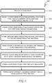
- FIG. 3 is a flowchart illustrating a method 300 of manufacturing a TFET according to an embodiment of the invention.
- method 300 may result in the formation of a TFET that is similar to TFET 100 or to TFET 200 that are shown, respectively, in FIGs. 1 and 2 .
- Many of the steps in method 300 may be accomplished according to techniques that are well known in the art. Where this is the case, the details of such techniques are not described in detail (or at all).
- a step 310 of method 300 is to provide a substrate.
- the substrate can be similar to substrate 205 that is shown in FIG. 2 .
- a step 320 of method 300 is to select a first semiconducting material that has type-II band alignment with a second semiconducting material.
- the first semiconducting material comprises a first Group III material and a first Group V material.
- the first semiconducting material comprises GaAs 0.5 Sb 0.5 .
- a step 330 of method 300 is to form a first semiconducting region containing the first semiconducting material.
- the first semiconducting region can be similar to source region 110 or to source region 210 that are shown, respectively, in FIGs. 1 and 2 .
- a step 340 of method 300 is to form a second semiconducting region containing the second semiconducting material.
- the second semiconducting region can be similar to channel region 130 or to channel region 230 that are shown, respectively, in FIGs. 1 and 2 .
- the second semiconducting material comprises a second Group III material and a second Group V material.
- the second Group III material can be the same as or different from the first Group III material.
- the second Group V material can be the same as or different from the first Group V material.
- step 330, step 340, or another step comprises lattice matching the first compound semiconductor and the second compound semiconductor to each other.
- the second semiconducting material comprises In 0.53 Ga 0.47 As.
- a step 350 of method 300 is to form a third semiconducting region containing a third semiconducting material.
- the third semiconducting region can be similar to drain region 120 or to drain region 220 that are shown, respectively, in FIGs. 1 and 2 .
- the third semiconducting material comprises a third Group III material and a third Group V material.
- the third Group III material can be the same as or different from the second and/or the first Group III material.
- the third Group V material can be the same as or different from the second and/or the first Group V material.
- Step 350 comprises selecting as the third semiconducting material a semiconducting material that has a charge neutrality level lying above a bottom of its conduction band.
- the third semiconducting material comprises In 0.53 Ga 0.47 As.
- a step 360 of method 300 is to deposit a gate insulator over at least a portion of at least the first semiconducting region.
- the gate insulator can be similar to gate insulator 145 or to gate insulator 245 that are shown, respectively, in FIGs. 1 and 2 .
- a step 370 of method 300 is to form a gate electrode over the gate insulator.
- the gate electrode can be similar to gate region 140 or to gate region 240 that are shown, respectively, in FIGs. 1 and 2 .
- a step 380 of method 300 is to form a gate contact, a source contact, and a drain contact for the TFET.
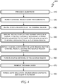
- FIG. 4 is a flowchart illustrating a method 400 of manufacturing a planar TFET according to an embodiment of the invention.
- method 400 may result in the formation of a TFET that is similar to TFET 200 that is shown in FIG. 2 .
- Method 400 may also result in the formation of a TFET 500 as described below and as illustrated in FIGs. 5-8 , which are cross-sectional views of TFET 500 at various stages of its manufacturing process according to an embodiment of the invention.
- Many of the steps in method 400 may be accomplished according to techniques that are well known in the art. Where this is the case, the details of such techniques are not described in detail (or at all).
- Planar TFET designs may be used to separate out source/gate or drain overlap capacitance that may be a characteristic of vertical TFET designs.
- a step 410 of method 400 is to provide a substrate.
- the substrate can be similar to substrate 205 that is shown in FIG. 2 .
- a step 420 of method 400 is to form a channel region over the substrate.
- the channel region can be similar to channel region 230 that is shown in FIG. 2 .
- the channel region can be similar to a channel region 530 that is first shown in FIG. 5 .
- step 420 comprises selecting a first semiconducting material to occupy the channel region, where the first semiconducting material has type-II band alignment with a second semiconducting material to be introduced below in step 460.
- step 420 comprises growing In 0.53 Ga 0.47 As.
- a step 430 of method 400 is to define a gate region over the channel region.
- the gate region can be similar to gate region 240 that is shown in FIG. 2 .
- the gate region can be similar to a gate region 540 that is first shown in FIG. 5 .
- step 430 comprises depositing (and later removing) a high-k or other gate insulator (such as a gate insulator 545 as first shown in FIG. 5 ) and a gate metal (such as a gate metal 546 as first shown in FIG. 5 ) and patterning them in order to define a sacrificial gate.
- a step 440 of method 400 is to implant and activate a first dopant species in order to define a source region and a drain region adjacent to the gate region and in order to form a drain material in the drain region.
- the source region and the channel region form a tunneling junction of the planar TFET along their adjacent sides.
- the first dopant species may be activated by an annealing process according to techniques known in the art, either as part of step 440 or at a different stage of method 400, perhaps following step 450 (as mentioned below).
- the source region and the drain region can be similar to, respectively, source regions 110 and 210 and drain regions 120 and 220, all of which are shown in FIGs. 1 or 2 .
- the implant of step 440 is depicted in FIG.
- step 440 comprises implanting the source region and the drain region with the doping species (e.g., n+) and then later etching out the source region to leave it open for a subsequent p+ implantation.
- the doping species e.g., n+
- Amorphized InGaAs for example, etches selectively compared to an epitaxial film so it may be helpful to this process if the source region is amorphosized by a high energy ion implantation prior to etching.
- the channel region and the drain region contain the same semiconducting material, so that where the channel region may contain, for example, undoped or lightly doped In 0.53 Ga 0.47 As, the drain region, following step 440, may contain more highly-doped In 0.53 Ga 0.47 As.
- FIG. 6 illustrates a result of step 440 according to one embodiment of the invention.
- the source region defined by step 440 can be similar to a source region 610, shown in FIG. 6
- the drain region defined by step 440 can be similar to a drain region 620, also shown in FIG. 6 .
- a step 450 of method 400 is to deposit a mask layer over the gate region and the channel region, leaving the source region exposed.
- the mask layer can be similar to a mask layer 701 that is shown in FIG. 7 .
- mask layer 701 can comprise silicon nitride (SiN).
- step 450 can be preceded by the removal of the sacrificial gate and followed by an implant activation anneal of the doped regions. In FIG. 7 , for example, the implanted material has been removed from source region 610, and mask layer 701 does not extend over source region 610.
- a step 460 of method 400 is to form a source material in the source region.
- step 460 comprises forming in the source region a second semiconducting material that has type-II band alignment with the first semiconducting material (introduced above in step 420).
- step 460 comprises growing GaAs 0.5 Sb 0.5 .
- step 460 can comprise the in-situ re-growth of a few nm of the first semiconducting material (e.g., InGaAs) followed by the re-growth of a source material such as in-situ p-doped GaAsSb. The source material will not grow on regions covered by the mask layer.
- a step 470 of method 400 is to remove the mask layer.
- FIG. 8 depicts TFET 500 following the performance of step 470 according to an embodiment of the invention.
- a step 480 of method 400 is to form a gate insulator, source/drain contacts, and a gate electrode.
- the gate insulator, the source/drain contacts, and the gate electrode can be similar to, respectively, gate insulators 145 and/or 245, source contacts/drain contacts 111, 211/121, 221, and gate regions 140 and/or 240, all of which are shown in FIGs. 1 or 2 .
- the performance of step 480 and other processing steps may result in a TFET that resembles TFET 200, shown in FIG. 2 .
- Method 400 is one method of constructing a planar TFET according to embodiments of the invention. Many other methods and variations are, of course, also possible. One of these additional methods will now be described. Device fabrication may begin with the growth of undoped (or lightly doped) InGaAs on buffer layers/substrate in a reactor. Lattice-matched p-type GaAsSb (lattice matched to InGaAs as well as InP) is then deposited in the reactor. Once the GaAsSb layer is grown, the wafer is removed from the vacuum chamber and a SiN mask is deposited. A source mesa is formed by conventional lithography, with etching performed up to somewhere in the bulk of undoped InGaAs.
Landscapes
- Insulated Gate Type Field-Effect Transistor (AREA)
- Thin Film Transistor (AREA)
- Junction Field-Effect Transistors (AREA)
Description
- The disclosed embodiments of the invention relate generally to tunnel field effect transistors, and relate more particularly to materials that may be used in such transistors.
- The Tunnel Field Effect Transistor, or TFET, is a device being studied for its potential to overcome certain obstacles in transistor manufacture and operation that are likely to arise at deep sub-micron microprocessor technology nodes. Among other potential advantages, it is anticipated that TFETs will help enable scaling to, for example, 22 nanometers (nm) because the threshold voltage (Vt) of a TFET is not limited by the discrete nature of dopants in the channel region with scaling, and because sub-threshold swing S can be lower than 60 millivolts/decade (mV/dec). As a result, the off-state leakage current (Ioff) can be significantly reduced below that of existing complementary metal-oxide semiconductors (CMOS) devices. TFETs also have high-speed switching capability.
- The TFET structure is close to that of a CMOS transistor. There are two types of TFET: n-type (NTFETs) and p-type (PTFETs). The drain current increases with increasing gate voltage (Vg) for an NTFET and increases with decreasing Vg for a PTFET. The NTFET switches on for gate-source voltage (Vgs) greater than Vt, while the PTFET switches on for Vgs less than Vt. The source in an NTFET is p-doped while the drain is n-doped and the source in a PTFET is n-doped while the drain is p-doped. A TFET shows exponentially increasing and temperature-independent characteristics at both off and on states. Unlike conventional CMOS devices, where sub-threshold swing S has a lower limit of 60 mV/dec at 300K, S in TFETs is independent of temperature. As a result, as mentioned above, off-state leakage can be significantly reduced. The threshold voltage in a TFET is controlled by the width and the height at the source end of the tunneling junction and is independent of the channel doping. The energy band gap at the tunnel junction determines the tunnel barrier height. It has also been demonstrated that the introduction of what is referred to as a delta layer between source and channel regions lowers the valence band offset and band gap at the tunneling junction with respect to the source region material. This decreases the tunneling barrier height, thus leading to higher tunneling probability.
-
EP1900681 addresses the problem of the large resistance of the tunnel barrier and achieving higher on-currents. It implements a nanowire-based TFET with a germanium (Ge) tunnel barrier in an otherwise silicon (Si) channel. A nanowire is introduced such that the lattice mismatch between silicon and germanium does not result in a highly defective interface. According to the document, a dynamic power reduction as well as a static power reduction can result, compared to conventional MOSFET configurations. Multiple layers of logic can therefore be envisioned with nanowire Si/Ge TFETs resulting in ultra-high on-chip transistor densities. JPS62209864 discloses a semiconductor device adapted to obtain a high-speed switch element which is not restricted in time constant by controlling a resonance transition current in a hetero junction to switch the current. The document goes on to disclose a GaSb single crystal 1 and an InAs single crystal 2 which form a hetero junction therebetween wherein the level Ev of the upper end of the valance band of the crystal 1 is higher than the level Ec of the bottom of a conduction band of the crystal.EP0549373 addresses the issue of suppressing the leak current of the gate by providing a structure where control of the tunnel current can be performed by applying a reverse bias voltage between the gate and the drain. It suggests a tunnel transistor which has a junction structure wherein a degenerated first semiconductor having one conduction type, a non-degenerated second semiconductor and a degenerated third semiconductor having the reverse conduction type to that of the first semiconductor are connected on a substrate or a laminated layer structure. The tunnel transistor of the document further includes a fourth semiconductor layer formed on an exposed surface of the second semiconductor, having a forbidden band wider than that of the second semiconductor and containing an ionized impurity therein, a gate electrode formed on the fourth semiconductor layer, and a pair of electrodes individually forming ohmic junctions to the first and third semiconductors. Due to the construction thereof, even when the gate voltage is 0, electrons or positive holes are induced in the surface of the second semiconductor, and a tunnel current can be flowed between the source and the drain. KATAYAMA T ET AL: "Structural dependence of intersubband absorption of In0.53Ga0.47As/GaAs0.5Sb0.5 type II quantum well structures lattice-matched to InP", JOURNAL OF CRYSTAL GROWTH, ELSEVIER, AMSTERDAM, NL, vol. 209, no. 2-3, 1 February 2000 (2000-02-01), pages 450-453, discloses a study of structural dependence of inter-subband absorption of the In0.53Ga0.47AsIGaAs0.5Sb0.5 multiple quantum well structure lattice-matched to InP substrates. According to the document, a clear inter-sub-band absorption with a narrow spectral linewidth was observed at room temperature. Based on the results obtained from the inter-sub-band absorption, an InGaAs/GaAsSb double barrier resonant tunnelling diode was fabricated, which shows a clear negative differential resistance at room temperature. - The disclosed embodiments will be better understood from a reading of the following detailed description, taken in conjunction with the accompanying figures in the drawings in which:
-
FIG. 1 is a cross-sectional view of a TFET according to an embodiment of the invention; -
FIG. 2 is a cross-sectional view of a TFET according to another embodiment of the invention; -
FIG. 3 is a flowchart illustrating a method of manufacturing a TFET according to an embodiment of the invention; -
FIG. 4 is a flowchart illustrating a method of manufacturing a planar TFET according to an embodiment of the invention; and -
FIGs. 5-8 are cross-sectional views of a planar TFET at various stages of its manufacturing process according to an embodiment of the invention. - For simplicity and clarity of illustration, the drawing figures illustrate the general manner of construction, and descriptions and details of well-known features and techniques may be omitted to avoid unnecessarily obscuring the discussion of the described embodiments of the invention. Additionally, elements in the drawing figures are not necessarily drawn to scale. For example, the dimensions of some of the elements in the figures may be exaggerated relative to other elements to help improve understanding of embodiments of the present invention. The same reference numerals in different figures denote the same elements, while similar reference numerals may, but do not necessarily, denote similar elements.
- The terms "first," "second," "third," "fourth," and the like in the description and in the claims, if any, are used for distinguishing between similar elements and not necessarily for describing a particular sequential or chronological order. It is to be understood that the terms so used are interchangeable under appropriate circumstances such that the embodiments of the invention described herein are, for example, capable of operation in sequences other than those illustrated or otherwise described herein. Similarly, if a method is described herein as comprising a series of steps, the order of such steps as presented herein is not necessarily the only order in which such steps may be performed, and certain of the stated steps may possibly be omitted and/or certain other steps not described herein may possibly be added to the method. Furthermore, the terms "comprise," "include," "have," and any variations thereof, are intended to cover a non-exclusive inclusion, such that a process, method, article, or apparatus that comprises a list of elements is not necessarily limited to those elements, but may include other elements not expressly listed or inherent to such process, method, article, or apparatus.
- The terms "left," "right," "front," "back," "top," "bottom," "over," "under," and the like in the description and in the claims, if any, are used for descriptive purposes and not necessarily for describing permanent relative positions. It is to be understood that the terms so used are interchangeable under appropriate circumstances such that the embodiments of the invention described herein are, for example, capable of operation in other orientations than those illustrated or otherwise described herein. The term "coupled," as used herein, is defined as directly or indirectly connected in an electrical or non-electrical manner. Objects described herein as being "adjacent to" each other may be in physical contact with each other, in close proximity to each other, or in the same general region or area as each other, as appropriate for the context in which the phrase is used. Occurrences of the phrase "in one embodiment" herein do not necessarily all refer to the same embodiment.
- In one embodiment of the invention, a TFET comprises a source region, a drain region, a channel region between the source region and the drain region, and a gate region adjacent to the channel region. The source region contains a first compound semiconductor comprising a first Group III material and a first Group V material, and the channel region contains a second compound semiconductor comprising a second Group III material and a second Group V material.
- Certain potential advantages of the TFET structure were mentioned above. These included a high-speed switching capability and the potential to overcome scaling limits of conventional CMOS transistors due, at least in part, to the temperature independence of sub-threshold swing S that enables a decrease in Ioff with device scaling. Existing TFETs, however, require high doping concentrations in source and drain regions in order to enhance tunneling current density, leading to the possible amorphosization of source and drain regions. As will be explained in detail below, embodiments of the invention offer a viable TFET manufacturing process utilizing easily-implemented III-V-based materials that eliminate implantation-induced damages.
- More specifically, embodiments of the invention exploit type-II band offsets, Fermi level pinning in the conduction band due to surface states, and crystalline re-growth characteristics of III-V semiconductors to fabricate a TFET. Characteristics of TFETs according to various embodiments of the invention may include a planar or vertical TFET with a III-V layer stack, a multi-layer stack as epitaxial component with type-II band alignments between adjacent layers, a drain (e.g., an n+ region) of material that typically pins in the conduction band, and in-situ doping of source and drain as opposed to high energy implantation.
- Referring now to the drawings,
FIG. 1 is a cross-sectional view of aTFET 100 according to an embodiment of the invention. As illustrated inFIG. 1 , TFET 100 comprises asource region 110 and adrain region 120 formed on a substrate (not shown), achannel region 130 betweensource region 110 anddrain region 120, and agate region 140 adjacent tochannel region 130. Agate insulator 145 electrically insulatesgate region 140 and the source, channel, and drain regions from each other. In one embodiment,gate region 140 contains a metal gate electrode andgate insulator 145 is a high-k dielectric material. In another embodiment,gate region 140 contains a polysilicon gate electrode andgate insulator 145 is an oxide material. - A
source contact 111 allows a voltage to be applied to sourceregion 110, and similar contacts are associated withdrain region 120 andgate region 140, namely, adrain contact 121 and agate contact 141, respectively. Aspacer 150caps gate region 140 andgate insulator 145. - For increased doping levels at the source-channel interface, a delta layer may be introduced. In the illustrated embodiment,
TFET 100 further comprises adelta layer 160 located betweensource region 110 andchannel region 130. A portion ofdelta layer 160 is thus located at atunneling junction 170 ofTFET 100.Delta layer 160 comprises a material that lowers at least one of the valence band offset and the band gap at tunneling junction 170 (which, as shown, is located at the ends of channel region 130). As mentioned above, lower valence band offsets and lower band gaps decrease tunneling barrier height and increase tunneling probability. In a particular embodiment,delta layer 170 comprises GaAs0.08Sb0.92. In the same or another embodiment,delta layer 170 is grown fully strained, i.e., is grown such that it does not exceed the critical layer thickness. -
Source region 110 contains a first compound semiconductor comprising a first Group III material and a first Group V material.Channel region 130 contains a second compound semiconductor comprising a second Group III material and a second Group V material. These materials may combine to create homojunctions, where source, channel and drain regions are of same material, or heterojunctions, where source, channel and drain regions are of at least two different materials. - According to one embodiment of the invention, the second compound semiconductor has type-II band alignment with the first compound semiconductor. As known in the art, this means that the band offsets are such that the valence band of the source region falls in the band gap of the channel region whereas the conduction band of source region is higher than the conduction band of the channel region. The effective band gap of the channel region is thus further reduced, tunneling probability is improved, and the need to have high source doping is eliminated in favor of the somewhat lower concentrations of in-situ doping. In-situ doping during source material deposition can easily be implemented according to standard techniques. In the same or another embodiment, the first compound semiconductor and the second compound semiconductor are lattice matched to each other. Examples of materials exhibiting the foregoing characteristics are given below.
- Since the band offsets are such that it is easier to move bands to align Fermi levels, considerably lower doping is needed, as mentioned above. The doping in the source/drain region could be as low as the 1x1016 cm-3 range. As also mentioned, this allows in-situ doping to be sufficient and eliminates the need to employ implantation with its possibility of amorphisization of the source and drain regions.
- The drain region 120 (in an NTFET) contains a material having a charge neutrality level that lies above a bottom of its conduction band. This means that its Fermi level pinning position is in the conduction band, i.e., it is an intrinsic semiconductor. Introducing layers which pin in the conduction band can diminish or eliminate the need for high doping in the drain. In one embodiment, the material of
drain region 120 comprises a third compound semiconductor such as InAs, InN, or the like. (The foregoing discussion also applies to the source region of a PTFET.) In a particular embodiment, In0.53Ga0.47As may be used for the third compound semiconductor, i.e., for the drain region of an NTFET, while GaAs0.5Sb0.5, and In0.53Ga0.47As may be used, respectively, for the first and second compound semiconductors of the NTFET, i.e., for the source and the channel regions. - Various materials and combinations of materials exhibit the properties discussed above and can be used for embodiments of the invention. Some of these have been mentioned above, and are repeated below. For example, for lattice matched homojunctions, narrow band gap materials with low effective mass such as InAs, InxGa1-xAs (for x ≥ 0.53), InSb, InN, InAsSb, and InGaN may be used, where In is indium, As is arsenic, Ga is gallium, Sb is antimony, and N is nitrogen. For lattice matched and mismatched heterojunctions, possible NTFET materials include GaAs0.5Sb0.5 for the source (or, in the language of the preceding paragraph, for the first compound semiconductor), In0.53Ga0.47As (or In0.53GaAs) for the channel (or, in the language of the preceding paragraph, for the second compound semiconductor), and InxGa1-xAs (or In0.53GaAs) for the drain, for x ≥ 0.53. More generally, source, channel, and drain materials may be respectively, GaSb, InGaAsSb, and InAs, or GaSb, InAs, and InAs. For lattice matched and mismatched heterojunctions with type-II band offsets, GaAs0.5Sb0.5, In0.53GaAs, and In0.53GaAs may be used, respectively, for source, channel, and drain regions. GaAs0.5Sb0.5 and In0.53Ga0.47As layers also have type-II band offsets. In embodiments having a delta layer, as mentioned above, the delta layer can comprise GaAs0.05Sb0.92.
- It should be noted here that layer thicknesses are not critical where homojunctions are concerned, but for heterojunctions there will be a critical layer thickness limit which must be observed when growing the layer on an underlying lattice-mismatched layer. As known in the art, defects may form in the layer being grown if the critical layer thickness is exceeded.
- Impact ionization is caused by the injection of tunneling electrons coming from a p+ source. The tunneling current and the impact ionization are dependent on the gate voltage. With no gate voltage, the electric field in the channel is small. Due to the band offsets given in the above proposed structures, chances of avalanche breakdown may be low in the intrinsic (lightly doped) region (the channel region) of such structures when the electric field in the channel is increased.
- Other TFET configurations are also possible. For example, the locations of
source region 110 and drainregion 120 could be switched inTFET 100, such thatdrain region 120 could be abovechannel region 130 andsource region 110 could be below. Both this and the illustrated embodiment ofTFET 100 are examples of a vertical TFET structure (or simply "vertical TFET"), so called because the source, channel, and drain regions are arranged vertically with respect to each other. Also possible are planar (or horizontal) TFETs, in which the source, channel, and drain regions are arranged horizontally with respect to each other. An example of a planar TFET structure is shown inFIG. 2 , which is a cross-sectional view of aTFET 200 according to an embodiment of the invention. Each of these alternate TFET configurations may be fabricated such that they share the characteristics and exhibit the advantages that were disclosed above forTFET 100. - It has been shown that the barrier height at a tunneling junction may be reduced by the introduction of a smaller band gap compound semiconductor (e.g., SiGe) at the source end in an otherwise homojunction Si TFET. Low band gap materials such as InAs, InAsSb and InSb have effective masses (m*) and band gap energies (Eg) that are much smaller than those of silicon and thus enable tunneling current that is expected to be much larger than that possible with silicon.
- As illustrated in
FIG. 2 ,TFET 200 comprises asubstrate 205, asource region 210 and adrain region 220 insubstrate 205, achannel region 230 betweensource region 210 and drainregion 220, and agate region 240 separated fromsubstrate 205 by agate insulator 245.Source region 110,drain region 120, andgate region 140 are contacted, respectively, by asource contact 211, adrain contact 221, and agate contact 241. Ifsubstrate 205 is lightly n-doped,source region 210 is p-doped, and drainregion 220 is n-doped,TFET 200 becomes an NTFET. If instead drainregion 220 is n-doped andsource region 210 is p-doped,TFET 200 becomes a PTFET. In that case,source region 110 and drainregion 120 may sit within a p-well (not shown) insubstrate 205. In both cases the tunneling junction is located at the end of the channel region nearest the source region. -
FIG. 3 is a flowchart illustrating amethod 300 of manufacturing a TFET according to an embodiment of the invention. As an example,method 300 may result in the formation of a TFET that is similar to TFET 100 or to TFET 200 that are shown, respectively, inFIGs. 1 and 2 . Many of the steps inmethod 300 may be accomplished according to techniques that are well known in the art. Where this is the case, the details of such techniques are not described in detail (or at all). - A
step 310 ofmethod 300 is to provide a substrate. As an example, the substrate can be similar tosubstrate 205 that is shown inFIG. 2 . - A
step 320 ofmethod 300 is to select a first semiconducting material that has type-II band alignment with a second semiconducting material. In one embodiment, the first semiconducting material comprises a first Group III material and a first Group V material. In a particular embodiment, the first semiconducting material comprises GaAs0.5Sb0.5. - A
step 330 ofmethod 300 is to form a first semiconducting region containing the first semiconducting material. As an example, the first semiconducting region can be similar tosource region 110 or to sourceregion 210 that are shown, respectively, inFIGs. 1 and 2 . - A
step 340 ofmethod 300 is to form a second semiconducting region containing the second semiconducting material. As an example, the second semiconducting region can be similar tochannel region 130 or to channelregion 230 that are shown, respectively, inFIGs. 1 and 2 . In one embodiment, the second semiconducting material comprises a second Group III material and a second Group V material. The second Group III material can be the same as or different from the first Group III material. Similarly, the second Group V material can be the same as or different from the first Group V material. In one embodiment,step 330,step 340, or another step comprises lattice matching the first compound semiconductor and the second compound semiconductor to each other. In a particular embodiment, the second semiconducting material comprises In0.53Ga0.47As. - A
step 350 ofmethod 300 is to form a third semiconducting region containing a third semiconducting material. As an example, the third semiconducting region can be similar to drainregion 120 or to drainregion 220 that are shown, respectively, inFIGs. 1 and 2 . In one embodiment, the third semiconducting material comprises a third Group III material and a third Group V material. The third Group III material can be the same as or different from the second and/or the first Group III material. Similarly, the third Group V material can be the same as or different from the second and/or the first Group V material. Step 350 comprises selecting as the third semiconducting material a semiconducting material that has a charge neutrality level lying above a bottom of its conduction band. In a particular embodiment, the third semiconducting material comprises In0.53Ga0.47As. - A
step 360 ofmethod 300 is to deposit a gate insulator over at least a portion of at least the first semiconducting region. As an example, the gate insulator can be similar togate insulator 145 or togate insulator 245 that are shown, respectively, inFIGs. 1 and 2 . - A
step 370 ofmethod 300 is to form a gate electrode over the gate insulator. As an example, the gate electrode can be similar togate region 140 or togate region 240 that are shown, respectively, inFIGs. 1 and 2 . - A
step 380 ofmethod 300 is to form a gate contact, a source contact, and a drain contact for the TFET. -
FIG. 4 is a flowchart illustrating amethod 400 of manufacturing a planar TFET according to an embodiment of the invention. As an example,method 400 may result in the formation of a TFET that is similar to TFET 200 that is shown inFIG. 2 .Method 400 may also result in the formation of aTFET 500 as described below and as illustrated inFIGs. 5-8 , which are cross-sectional views ofTFET 500 at various stages of its manufacturing process according to an embodiment of the invention. Many of the steps inmethod 400 may be accomplished according to techniques that are well known in the art. Where this is the case, the details of such techniques are not described in detail (or at all). Planar TFET designs may be used to separate out source/gate or drain overlap capacitance that may be a characteristic of vertical TFET designs. - A
step 410 ofmethod 400 is to provide a substrate. As an example, the substrate can be similar tosubstrate 205 that is shown inFIG. 2 . - A
step 420 ofmethod 400 is to form a channel region over the substrate. As an example, the channel region can be similar tochannel region 230 that is shown inFIG. 2 . As another example, the channel region can be similar to achannel region 530 that is first shown inFIG. 5 . In one embodiment,step 420 comprises selecting a first semiconducting material to occupy the channel region, where the first semiconducting material has type-II band alignment with a second semiconducting material to be introduced below instep 460. In a particular embodiment,step 420 comprises growing In0.53Ga0.47As. - A
step 430 ofmethod 400 is to define a gate region over the channel region. As an example, the gate region can be similar togate region 240 that is shown inFIG. 2 . As another example, the gate region can be similar to agate region 540 that is first shown inFIG. 5 . In one embodiment,step 430 comprises depositing (and later removing) a high-k or other gate insulator (such as agate insulator 545 as first shown inFIG. 5 ) and a gate metal (such as agate metal 546 as first shown inFIG. 5 ) and patterning them in order to define a sacrificial gate. - A
step 440 ofmethod 400 is to implant and activate a first dopant species in order to define a source region and a drain region adjacent to the gate region and in order to form a drain material in the drain region. The source region and the channel region form a tunneling junction of the planar TFET along their adjacent sides. The first dopant species may be activated by an annealing process according to techniques known in the art, either as part ofstep 440 or at a different stage ofmethod 400, perhaps following step 450 (as mentioned below). As an example, the source region and the drain region can be similar to, respectively,source regions drain regions FIGs. 1 or 2 . The implant ofstep 440 is depicted inFIG. 5 with arrows representing an n-type or a p-type implant event. In one embodiment,step 440 comprises implanting the source region and the drain region with the doping species (e.g., n+) and then later etching out the source region to leave it open for a subsequent p+ implantation. Amorphized InGaAs, for example, etches selectively compared to an epitaxial film so it may be helpful to this process if the source region is amorphosized by a high energy ion implantation prior to etching. - In various embodiments, as mentioned above, the channel region and the drain region contain the same semiconducting material, so that where the channel region may contain, for example, undoped or lightly doped In0.53Ga0.47As, the drain region, following
step 440, may contain more highly-doped In0.53Ga0.47As.FIG. 6 illustrates a result ofstep 440 according to one embodiment of the invention. As an example, the source region defined bystep 440 can be similar to asource region 610, shown inFIG. 6 , and the drain region defined bystep 440 can be similar to adrain region 620, also shown inFIG. 6 . - A
step 450 ofmethod 400 is to deposit a mask layer over the gate region and the channel region, leaving the source region exposed. As an example, the mask layer can be similar to amask layer 701 that is shown inFIG. 7 . In one embodiment,mask layer 701 can comprise silicon nitride (SiN). In one embodiment, step 450 can be preceded by the removal of the sacrificial gate and followed by an implant activation anneal of the doped regions. InFIG. 7 , for example, the implanted material has been removed fromsource region 610, andmask layer 701 does not extend oversource region 610. - A
step 460 ofmethod 400 is to form a source material in the source region. In one embodiment,step 460 comprises forming in the source region a second semiconducting material that has type-II band alignment with the first semiconducting material (introduced above in step 420). In a particular embodiment,step 460 comprises growing GaAs0.5Sb0.5. As an example, step 460 can comprise the in-situ re-growth of a few nm of the first semiconducting material (e.g., InGaAs) followed by the re-growth of a source material such as in-situ p-doped GaAsSb. The source material will not grow on regions covered by the mask layer. - A
step 470 ofmethod 400 is to remove the mask layer.FIG. 8 depictsTFET 500 following the performance ofstep 470 according to an embodiment of the invention. - A
step 480 ofmethod 400 is to form a gate insulator, source/drain contacts, and a gate electrode. As an example, the gate insulator, the source/drain contacts, and the gate electrode can be similar to, respectively,gate insulators 145 and/or 245, source contacts/drain contacts gate regions 140 and/or 240, all of which are shown inFIGs. 1 or 2 . The performance ofstep 480 and other processing steps may result in a TFET that resemblesTFET 200, shown inFIG. 2 . -
Method 400 is one method of constructing a planar TFET according to embodiments of the invention. Many other methods and variations are, of course, also possible. One of these additional methods will now be described. Device fabrication may begin with the growth of undoped (or lightly doped) InGaAs on buffer layers/substrate in a reactor. Lattice-matched p-type GaAsSb (lattice matched to InGaAs as well as InP) is then deposited in the reactor. Once the GaAsSb layer is grown, the wafer is removed from the vacuum chamber and a SiN mask is deposited. A source mesa is formed by conventional lithography, with etching performed up to somewhere in the bulk of undoped InGaAs. The wafer is then sent to the reactor and re-growth of undoped InGaAs follows. There is no growth of InGaAs on the SiN layer. After a few nm of InGaAs, n+ InxGa1-xAs (x=0.53) or strained InxGa1-xAs (x > 0.53) drain is deposited. The rest of the device fabrication is carried out to deposit gate oxide, S/D and gate.
Claims (15)
- A tunnel field effect transistor comprising:a source region (110);a drain region (120);a channel region (130) between the source region and the drain region; anda gate region (140) adjacent to the channel region, wherein:the source region contains a first compound semiconductor comprising a first Group III material and a first Group V material; andthe channel region contains a second compound semiconductor comprising a second Group III material and a second Group V material;characterised in thatthe drain region contains a material having a charge neutrality level that lies above a bottom of its conduction band.
- The tunnel field effect transistor of claim 1 wherein:the second compound semiconductor has type-II band alignment with the first compound semiconductor.
- The tunnel field effect transistor of claim 1 wherein:the first compound semiconductor and the second compound semiconductor are lattice matched to each other.
- The tunnel field effect transistor of claim 1 wherein:the first compound semiconductor is GaAs0.5Sb0.5; and the second compound semiconductor is In0.53Ga0.47As.
- The tunnel field effect transistor of claim 4 wherein:the drain region comprises a third compound semiconductor; and the third compound semiconductor is In0.53Ga0.47As.
- The tunnel field effect transistor of claim 4 further comprising:a delta layer (160) between the source region and the channel region.
- The tunnel field effect transistor of claim 6 wherein:the delta layer is located at a junction of the source region and the channel region;the junction is a tunneling junction of the tunnel field effect transistor; and the delta layer comprises a material that lowers at least one of a valence band offset and a band gap at the tunneling junction, and preferably wherein: the delta layer comprises GaAs0.8Sb0.92; and the delta layer is fully strained.
- A tunnel field effect transistor of claim 2 comprising:a substrate (205);wherein the source region is formed over the substrate;wherein the drain region is formed over the substrate.
- The tunnel field effect transistor of claim 8 wherein:the source region and the channel region are arranged vertically above the substrate such that all of the source region is above all of the channel region; orwherein:the source region and the channel region are arranged horizontally above the substrate such that no portion of the source region is above all of the channel region and no portion of the channel region is above all of the source region; orwherein:the first semiconducting material and the second semiconducting material are lattice matched to each other; orwherein:the drain region contains a third semiconducting material;the first semiconducting material is GaAs0.5Sb0.5;the second semiconducting material is In0.53Ga0.47As; andthe third semiconducting material is In0.53Ga0.47As.
- The tunnel field effect transistor of claim 8 wherein:a junction of the source region and the channel region comprises a tunneling junction of the tunnel field effect transistor;the tunnel field effect transistor further comprises a delta layer at the tunneling junction;the delta layer comprises a material that lowers a valence band offset and a band gap at the tunneling junction; andthe delta layer is fully strained, wherein preferably:the delta layer comprises GaAs0.8Sb0.92.
- A method of manufacturing a tunnel field effect transistor, the method comprising:providing a substrate;selecting a first semiconducting material, wherein the first semiconducting material comprises a first Group III material and a first Group V material;forming a first semiconducting region containing the first semiconducting material;forming a second semiconducting region containing the second semiconducting material, wherein the second semiconducting material comprises a second Group III material and a second Group V material;forming a third semiconducting region containing a third semiconducting material, wherein forming the third semiconducting region comprises selecting as the third semiconducting material a semiconducting material that has a charge neutrality level lying above a bottom of its conduction band;depositing a gate insulator over at least a portion of at least the first semiconducting region;forming a gate electrode over the gate insulator; andforming a gate contact, a source contact, and a drain contact for the tunnel field effect transistor.
- The method of claim 11 wherein:the first semiconducting material has type-II band alignment with a second semiconducting material; andthe third semiconducting material comprises a third Group III material and a third Group V material; orfurther comprising:lattice matching the first semiconducting material and the second semiconducting material to each other; orwherein:selecting the first semiconducting material comprises selecting GaAs0.5Sb0.5;
the second semiconducting material comprises In0.53Ga0.47As; and the third semiconducting material comprises In0.53Ga0.47As. - A method of claim 11, the method further comprising:forming a channel region over the substrate;defining a gate region over the channel region;implanting a first dopant species in order to define a source region and a drain region adjacent to the gate region and in order to form a drain material in the drain region;depositing a mask layer over the gate region and the channel region, leaving the source region exposed;forming a source material in the source region;removing the mask layer; andforming a gate insulator, source/drain contacts, and a gate electrode, wherein:the source region and the channel region form a tunneling junction of the planar tunnel field effect transistor along their adjacent sides.
- The method of claim 13 wherein:forming the channel region comprises selecting a first semiconducting material to occupy the channel region;forming the source material in the source region comprises forming a second semiconducting material in the source region; andthe first semiconducting material has type-II band alignment with the second semiconducting material.
- The method of claim 14, wherein:forming the channel region comprises growing In0.53Ga0.47As;forming the source material comprises growing GaAs0.5Sb0.5;forming the drain material comprises growing In0.53Ga0.47As.
Applications Claiming Priority (2)
| Application Number | Priority Date | Filing Date | Title |
|---|---|---|---|
| US12/319,102 US8026509B2 (en) | 2008-12-30 | 2008-12-30 | Tunnel field effect transistor and method of manufacturing same |
| PCT/US2009/068550 WO2010078054A2 (en) | 2008-12-30 | 2009-12-17 | Tunnel field effect transistor and method of manufacturing same |
Publications (3)
| Publication Number | Publication Date |
|---|---|
| EP2382667A2 EP2382667A2 (en) | 2011-11-02 |
| EP2382667A4 EP2382667A4 (en) | 2014-01-15 |
| EP2382667B1 true EP2382667B1 (en) | 2017-01-25 |
Family
ID=42283730
Family Applications (1)
| Application Number | Title | Priority Date | Filing Date |
|---|---|---|---|
| EP09836962.2A Not-in-force EP2382667B1 (en) | 2008-12-30 | 2009-12-17 | Tunnel field effect transistor and method of manufacturing same |
Country Status (7)
| Country | Link |
|---|---|
| US (2) | US8026509B2 (en) |
| EP (1) | EP2382667B1 (en) |
| JP (1) | JP5701774B2 (en) |
| KR (1) | KR101307191B1 (en) |
| CN (1) | CN102272933B (en) |
| TW (1) | TWI436478B (en) |
| WO (1) | WO2010078054A2 (en) |
Families Citing this family (49)
| Publication number | Priority date | Publication date | Assignee | Title |
|---|---|---|---|---|
| US8026509B2 (en) | 2008-12-30 | 2011-09-27 | Intel Corporation | Tunnel field effect transistor and method of manufacturing same |
| EP2267782A3 (en) * | 2009-06-24 | 2013-03-13 | Imec | Control of tunneling junction in a hetero tunnel field effect transistor |
| CN101777499B (en) * | 2010-01-22 | 2011-08-24 | 北京大学 | Method for self-aligned preparation of tunneling field-effect transistors (TFETs) on basis of planar technology |
| US8890118B2 (en) * | 2010-12-17 | 2014-11-18 | Intel Corporation | Tunnel field effect transistor |
| CN102194884B (en) * | 2011-04-26 | 2013-08-14 | 北京大学 | Field effect transistor of hybrid conduction mechanism |
| CN102222686A (en) * | 2011-06-28 | 2011-10-19 | 复旦大学 | Fence-type grid-controlled metal-insulator device based on electronic tunneling |
| JP5936247B2 (en) * | 2011-07-22 | 2016-06-22 | インターナショナル・ビジネス・マシーンズ・コーポレーションInternational Business Machines Corporation | Tunnel field effect transistor |
| GB2506831B (en) * | 2011-08-16 | 2015-09-02 | Fox Int Group Ltd | A method feeder |
| CN102403233B (en) * | 2011-12-12 | 2014-06-11 | 复旦大学 | Method for manufacturing tunnel transistor of vertical channel |
| US9136363B2 (en) | 2011-12-30 | 2015-09-15 | Seoul National University R&Db Foundation | Compound tunneling field effect transistor integrated on silicon substrate and method for fabricating the same |
| WO2013123287A1 (en) * | 2012-02-15 | 2013-08-22 | Steven May | Charge ordered vertical transistors |
| US9865716B2 (en) | 2012-08-24 | 2018-01-09 | Taiwan Semiconductor Manufacturing Company, Ltd. | System and method for a vertical tunneling field-effect transistor cell |
| US9209288B2 (en) | 2012-12-21 | 2015-12-08 | Intel Corporation | Reduced scale resonant tunneling field effect transistor |
| US9159826B2 (en) * | 2013-01-18 | 2015-10-13 | Taiwan Semiconductor Manufacturing Company, Ltd. | Vertical tunneling field-effect transistor cell and fabricating the same |
| US9029940B2 (en) * | 2013-01-18 | 2015-05-12 | Taiwan Semiconductor Manufacturing Company, Ltd. | Vertical tunneling field-effect transistor cell |
| US8975123B2 (en) | 2013-07-09 | 2015-03-10 | International Business Machines Corporation | Tunnel field-effect transistors with a gate-swing broken-gap heterostructure |
| JP5886802B2 (en) | 2013-08-29 | 2016-03-16 | 株式会社東芝 | Semiconductor device |
| US9425296B2 (en) * | 2013-09-09 | 2016-08-23 | Qualcomm Incorporated | Vertical tunnel field effect transistor |
| US9570609B2 (en) | 2013-11-01 | 2017-02-14 | Samsung Electronics Co., Ltd. | Crystalline multiple-nanosheet strained channel FETs and methods of fabricating the same |
| US9484423B2 (en) | 2013-11-01 | 2016-11-01 | Samsung Electronics Co., Ltd. | Crystalline multiple-nanosheet III-V channel FETs |
| JP2015095568A (en) | 2013-11-12 | 2015-05-18 | 株式会社東芝 | Semiconductor device |
| CN104701374B (en) * | 2013-12-10 | 2017-11-03 | 中芯国际集成电路制造(上海)有限公司 | Tunneling field-effect transistor and forming method thereof |
| JP6331375B2 (en) * | 2013-12-17 | 2018-05-30 | 富士通株式会社 | Field effect semiconductor device |
| KR102157825B1 (en) | 2014-01-16 | 2020-09-18 | 삼성전자주식회사 | Tunneling field effect transistor |
| KR20150085663A (en) * | 2014-01-16 | 2015-07-24 | 삼성전자주식회사 | Tunneling field effect transistor |
| CN103779418B (en) * | 2014-02-08 | 2016-08-31 | 华为技术有限公司 | A kind of tunneling field-effect transistor and preparation method thereof |
| US9425312B2 (en) | 2014-06-23 | 2016-08-23 | International Business Machines Corporation | Silicon-containing, tunneling field-effect transistor including III-N source |
| CN104134695A (en) * | 2014-07-15 | 2014-11-05 | 华为技术有限公司 | Tunneling field effect transistor and manufacturing method thereof |
| US9647098B2 (en) | 2014-07-21 | 2017-05-09 | Samsung Electronics Co., Ltd. | Thermionically-overdriven tunnel FETs and methods of fabricating the same |
| CN105633147A (en) * | 2014-10-27 | 2016-06-01 | 中国科学院微电子研究所 | Tunneling field effect transistor and manufacturing method thereof |
| CN104332502B (en) * | 2014-11-07 | 2017-06-06 | 华为技术有限公司 | A kind of complementary tunneling field-effect transistor and preparation method thereof |
| CN104617137B (en) * | 2015-01-19 | 2018-09-21 | 华为技术有限公司 | A kind of fieldtron and preparation method thereof |
| CN104617138B (en) * | 2015-01-26 | 2017-12-08 | 华为技术有限公司 | Tunneling field-effect transistor and preparation method thereof |
| CN105990409B (en) * | 2015-02-11 | 2019-01-08 | 中国科学院微电子研究所 | Preparation method of multi-layer tunnel junction three-dimensional tunnel field effect transistor |
| US9614042B2 (en) | 2015-03-06 | 2017-04-04 | International Business Machines Corporation | Heterojunction tunnel field effect transistor fabrication using limited lithography steps |
| JP6429688B2 (en) * | 2015-03-12 | 2018-11-28 | 国立研究開発法人物質・材料研究機構 | Tunnel field effect transistor and method of using the same |
| JP6377556B2 (en) * | 2015-03-19 | 2018-08-22 | 株式会社東芝 | Semiconductor device and semiconductor memory device |
| US9905647B2 (en) * | 2015-10-28 | 2018-02-27 | University Of Notre Dame Du Lac | Group III-nitride compound heterojunction tunnel field-effect transistors and methods for making the same |
| WO2017079979A1 (en) | 2015-11-13 | 2017-05-18 | 华为技术有限公司 | Tunnel field-effect transistor, and manufacturing method thereof |
| CN105576033A (en) * | 2016-03-04 | 2016-05-11 | 西安电子科技大学 | Ferroelectric tunneling field effect transistor based on InAs material and preparation method thereof |
| US10424581B2 (en) * | 2016-04-18 | 2019-09-24 | Samsung Electronics Co., Ltd. | Sub 59 MV/decade SI CMOS compatible tunnel FET as footer transistor for power gating |
| US9954101B2 (en) | 2016-06-15 | 2018-04-24 | International Business Machines Corporation | Precise junction placement in vertical semiconductor devices using etch stop layers |
| CN106129106A (en) * | 2016-07-01 | 2016-11-16 | 西安电子科技大学 | Mos field effect transistor and preparation method thereof |
| JP6826003B2 (en) * | 2017-06-26 | 2021-02-03 | 日本電信電話株式会社 | Tunnel field effect transistor |
| US11075107B2 (en) * | 2018-09-28 | 2021-07-27 | Taiwan Semiconductor Manufacturing Company Ltd. | Semiconductor structure and manufacturing method thereof |
| KR102198765B1 (en) * | 2019-01-29 | 2021-01-05 | 한국과학기술원 | Vertical type transistor with hetero-junction structure and method for manufacturing same |
| WO2020261471A1 (en) * | 2019-06-27 | 2020-12-30 | 日本電信電話株式会社 | Tunnel field-effect transistor and method for manufacturing same |
| KR102451562B1 (en) * | 2021-03-23 | 2022-10-06 | 한국과학기술원 | Tunneling field effect transistor and semiconductor device including the same |
| CN121038327B (en) * | 2025-10-31 | 2026-01-09 | 深圳平湖实验室 | Transistor and electronic equipment |
Family Cites Families (15)
| Publication number | Priority date | Publication date | Assignee | Title |
|---|---|---|---|---|
| JPS5775464A (en) * | 1980-10-28 | 1982-05-12 | Semiconductor Res Found | Semiconductor device controlled by tunnel injection |
| DE3477624D1 (en) * | 1984-12-18 | 1989-05-11 | Ibm | Low temperature tunneling transistor |
| JPS62209864A (en) * | 1986-03-11 | 1987-09-16 | Fujitsu Ltd | Semiconductor device |
| JPS63276277A (en) * | 1987-05-08 | 1988-11-14 | Fujitsu Ltd | Semiconductor negative differential resistance element |
| JPS63288061A (en) * | 1987-05-20 | 1988-11-25 | Fujitsu Ltd | Semiconductor negative resistance element |
| DE69202554T2 (en) * | 1991-12-25 | 1995-10-19 | Nippon Electric Co | Tunnel transistor and its manufacturing process. |
| US5883404A (en) * | 1994-08-29 | 1999-03-16 | Motorola, Inc. | Complementary heterojunction semiconductor device |
| JP2817718B2 (en) * | 1996-08-02 | 1998-10-30 | 日本電気株式会社 | Tunnel transistor and manufacturing method thereof |
| US6992337B2 (en) * | 2004-04-02 | 2006-01-31 | Agilent Technologies, Inc. | Gallium arsenide antimonide (GaAsSB)/indium phosphide (InP) heterojunction bipolar transistor (HBT) having reduced tunneling probability |
| US8441000B2 (en) * | 2006-02-01 | 2013-05-14 | International Business Machines Corporation | Heterojunction tunneling field effect transistors, and methods for fabricating the same |
| EP1900681B1 (en) | 2006-09-15 | 2017-03-15 | Imec | Tunnel Field-Effect Transistors based on silicon nanowires |
| EP2122687A1 (en) * | 2006-12-15 | 2009-11-25 | Nxp B.V. | Transistor device and method of manufacturing such a transistor device |
| FR2912838B1 (en) | 2007-02-15 | 2009-06-05 | Commissariat Energie Atomique | METHOD FOR PRODUCING A TRANSISTOR GRID |
| US8148718B2 (en) * | 2007-05-31 | 2012-04-03 | The Regents Of The University Of California | Low voltage transistors |
| US8026509B2 (en) | 2008-12-30 | 2011-09-27 | Intel Corporation | Tunnel field effect transistor and method of manufacturing same |
-
2008
- 2008-12-30 US US12/319,102 patent/US8026509B2/en active Active
-
2009
- 2009-12-17 JP JP2011544473A patent/JP5701774B2/en not_active Expired - Fee Related
- 2009-12-17 KR KR1020117015170A patent/KR101307191B1/en not_active Expired - Fee Related
- 2009-12-17 CN CN200980153845.1A patent/CN102272933B/en not_active Expired - Fee Related
- 2009-12-17 WO PCT/US2009/068550 patent/WO2010078054A2/en not_active Ceased
- 2009-12-17 EP EP09836962.2A patent/EP2382667B1/en not_active Not-in-force
- 2009-12-22 TW TW098144174A patent/TWI436478B/en not_active IP Right Cessation
-
2011
- 2011-09-02 US US13/224,661 patent/US8686402B2/en not_active Expired - Fee Related
Non-Patent Citations (1)
| Title |
|---|
| None * |
Also Published As
| Publication number | Publication date |
|---|---|
| US20100163845A1 (en) | 2010-07-01 |
| US20110315960A1 (en) | 2011-12-29 |
| WO2010078054A3 (en) | 2010-10-07 |
| KR101307191B1 (en) | 2013-09-11 |
| US8686402B2 (en) | 2014-04-01 |
| CN102272933A (en) | 2011-12-07 |
| JP2012514345A (en) | 2012-06-21 |
| WO2010078054A2 (en) | 2010-07-08 |
| TW201030977A (en) | 2010-08-16 |
| US8026509B2 (en) | 2011-09-27 |
| TWI436478B (en) | 2014-05-01 |
| JP5701774B2 (en) | 2015-04-15 |
| EP2382667A2 (en) | 2011-11-02 |
| CN102272933B (en) | 2013-11-06 |
| EP2382667A4 (en) | 2014-01-15 |
| KR20110089884A (en) | 2011-08-09 |
Similar Documents
| Publication | Publication Date | Title |
|---|---|---|
| US8026509B2 (en) | Tunnel field effect transistor and method of manufacturing same | |
| US8119488B2 (en) | Scalable quantum well device and method for manufacturing the same | |
| US7947557B2 (en) | Heterojunction tunneling field effect transistors, and methods for fabricating the same | |
| Riel et al. | InAs-Si heterojunction nanowire tunnel diodes and tunnel FETs | |
| US8324661B2 (en) | Quantum well transistors with remote counter doping | |
| US6963090B2 (en) | Enhancement mode metal-oxide-semiconductor field effect transistor | |
| US9960232B2 (en) | Horizontal nanosheet FETs and methods of manufacturing the same | |
| US20130264544A1 (en) | Nanowire field-effect device with multiple gates | |
| US8017933B2 (en) | Compositionally-graded quantum-well channels for semiconductor devices | |
| EP0549373B1 (en) | Tunnel transistor and method of manufacturing same | |
| US9773904B2 (en) | Vertical field effect transistor with biaxial stressor layer | |
| US20010005016A1 (en) | Field effect transistor | |
| US8441037B2 (en) | Semiconductor device having a thin film stacked structure | |
| US8575595B2 (en) | P-type semiconductor devices | |
| JPH05152339A (en) | Semiconductor device | |
| HK1175887B (en) | Techniques for forming contacts to quantum well transistors | |
| HK1175588A1 (en) | Quantum-well-based semiconductor devices | |
| HK1165904B (en) | Apparatus and methods for improving parallel conduction in a quantum well device | |
| HK1165904A1 (en) | Apparatus and methods for improving parallel conduction in a quantum well device |
Legal Events
| Date | Code | Title | Description |
|---|---|---|---|
| PUAI | Public reference made under article 153(3) epc to a published international application that has entered the european phase |
Free format text: ORIGINAL CODE: 0009012 |
|
| 17P | Request for examination filed |
Effective date: 20110729 |
|
| AK | Designated contracting states |
Kind code of ref document: A2 Designated state(s): AT BE BG CH CY CZ DE DK EE ES FI FR GB GR HR HU IE IS IT LI LT LU LV MC MK MT NL NO PL PT RO SE SI SK SM TR |
|
| DAX | Request for extension of the european patent (deleted) | ||
| REG | Reference to a national code |
Ref country code: DE Ref legal event code: R079 Ref document number: 602009044022 Country of ref document: DE Free format text: PREVIOUS MAIN CLASS: H01L0029780000 Ipc: H01L0029739000 |
|
| A4 | Supplementary search report drawn up and despatched |
Effective date: 20131217 |
|
| RIC1 | Information provided on ipc code assigned before grant |
Ipc: H01L 29/739 20060101AFI20131211BHEP |
|
| GRAP | Despatch of communication of intention to grant a patent |
Free format text: ORIGINAL CODE: EPIDOSNIGR1 |
|
| INTG | Intention to grant announced |
Effective date: 20160726 |
|
| GRAS | Grant fee paid |
Free format text: ORIGINAL CODE: EPIDOSNIGR3 |
|
| STAA | Information on the status of an ep patent application or granted ep patent |
Free format text: STATUS: GRANT OF PATENT IS INTENDED |
|
| GRAJ | Information related to disapproval of communication of intention to grant by the applicant or resumption of examination proceedings by the epo deleted |
Free format text: ORIGINAL CODE: EPIDOSDIGR1 |
|
| GRAL | Information related to payment of fee for publishing/printing deleted |
Free format text: ORIGINAL CODE: EPIDOSDIGR3 |
|
| STAA | Information on the status of an ep patent application or granted ep patent |
Free format text: STATUS: REQUEST FOR EXAMINATION WAS MADE |
|
| GRAR | Information related to intention to grant a patent recorded |
Free format text: ORIGINAL CODE: EPIDOSNIGR71 |
|
| INTC | Intention to grant announced (deleted) | ||
| STAA | Information on the status of an ep patent application or granted ep patent |
Free format text: STATUS: GRANT OF PATENT IS INTENDED |
|
| GRAA | (expected) grant |
Free format text: ORIGINAL CODE: 0009210 |
|
| STAA | Information on the status of an ep patent application or granted ep patent |
Free format text: STATUS: THE PATENT HAS BEEN GRANTED |
|
| AK | Designated contracting states |
Kind code of ref document: B1 Designated state(s): AT BE BG CH CY CZ DE DK EE ES FI FR GB GR HR HU IE IS IT LI LT LU LV MC MK MT NL NO PL PT RO SE SI SK SM TR |
|
| INTG | Intention to grant announced |
Effective date: 20161221 |
|
| REG | Reference to a national code |
Ref country code: GB Ref legal event code: FG4D |
|
| REG | Reference to a national code |
Ref country code: CH Ref legal event code: EP |
|
| REG | Reference to a national code |
Ref country code: AT Ref legal event code: REF Ref document number: 864572 Country of ref document: AT Kind code of ref document: T Effective date: 20170215 |
|
| REG | Reference to a national code |
Ref country code: IE Ref legal event code: FG4D |
|
| REG | Reference to a national code |
Ref country code: DE Ref legal event code: R096 Ref document number: 602009044022 Country of ref document: DE |
|
| REG | Reference to a national code |
Ref country code: NL Ref legal event code: FP |
|
| REG | Reference to a national code |
Ref country code: LT Ref legal event code: MG4D |
|
| REG | Reference to a national code |
Ref country code: AT Ref legal event code: MK05 Ref document number: 864572 Country of ref document: AT Kind code of ref document: T Effective date: 20170125 |
|
| PG25 | Lapsed in a contracting state [announced via postgrant information from national office to epo] |
Ref country code: LT Free format text: LAPSE BECAUSE OF FAILURE TO SUBMIT A TRANSLATION OF THE DESCRIPTION OR TO PAY THE FEE WITHIN THE PRESCRIBED TIME-LIMIT Effective date: 20170125 Ref country code: NO Free format text: LAPSE BECAUSE OF FAILURE TO SUBMIT A TRANSLATION OF THE DESCRIPTION OR TO PAY THE FEE WITHIN THE PRESCRIBED TIME-LIMIT Effective date: 20170425 Ref country code: FI Free format text: LAPSE BECAUSE OF FAILURE TO SUBMIT A TRANSLATION OF THE DESCRIPTION OR TO PAY THE FEE WITHIN THE PRESCRIBED TIME-LIMIT Effective date: 20170125 Ref country code: HR Free format text: LAPSE BECAUSE OF FAILURE TO SUBMIT A TRANSLATION OF THE DESCRIPTION OR TO PAY THE FEE WITHIN THE PRESCRIBED TIME-LIMIT Effective date: 20170125 Ref country code: IS Free format text: LAPSE BECAUSE OF FAILURE TO SUBMIT A TRANSLATION OF THE DESCRIPTION OR TO PAY THE FEE WITHIN THE PRESCRIBED TIME-LIMIT Effective date: 20170525 Ref country code: GR Free format text: LAPSE BECAUSE OF FAILURE TO SUBMIT A TRANSLATION OF THE DESCRIPTION OR TO PAY THE FEE WITHIN THE PRESCRIBED TIME-LIMIT Effective date: 20170426 |
|
| PG25 | Lapsed in a contracting state [announced via postgrant information from national office to epo] |
Ref country code: SE Free format text: LAPSE BECAUSE OF FAILURE TO SUBMIT A TRANSLATION OF THE DESCRIPTION OR TO PAY THE FEE WITHIN THE PRESCRIBED TIME-LIMIT Effective date: 20170125 Ref country code: LV Free format text: LAPSE BECAUSE OF FAILURE TO SUBMIT A TRANSLATION OF THE DESCRIPTION OR TO PAY THE FEE WITHIN THE PRESCRIBED TIME-LIMIT Effective date: 20170125 Ref country code: ES Free format text: LAPSE BECAUSE OF FAILURE TO SUBMIT A TRANSLATION OF THE DESCRIPTION OR TO PAY THE FEE WITHIN THE PRESCRIBED TIME-LIMIT Effective date: 20170125 Ref country code: PL Free format text: LAPSE BECAUSE OF FAILURE TO SUBMIT A TRANSLATION OF THE DESCRIPTION OR TO PAY THE FEE WITHIN THE PRESCRIBED TIME-LIMIT Effective date: 20170125 Ref country code: PT Free format text: LAPSE BECAUSE OF FAILURE TO SUBMIT A TRANSLATION OF THE DESCRIPTION OR TO PAY THE FEE WITHIN THE PRESCRIBED TIME-LIMIT Effective date: 20170525 Ref country code: AT Free format text: LAPSE BECAUSE OF FAILURE TO SUBMIT A TRANSLATION OF THE DESCRIPTION OR TO PAY THE FEE WITHIN THE PRESCRIBED TIME-LIMIT Effective date: 20170125 Ref country code: BG Free format text: LAPSE BECAUSE OF FAILURE TO SUBMIT A TRANSLATION OF THE DESCRIPTION OR TO PAY THE FEE WITHIN THE PRESCRIBED TIME-LIMIT Effective date: 20170425 |
|
| REG | Reference to a national code |
Ref country code: DE Ref legal event code: R097 Ref document number: 602009044022 Country of ref document: DE |
|
| PG25 | Lapsed in a contracting state [announced via postgrant information from national office to epo] |
Ref country code: SK Free format text: LAPSE BECAUSE OF FAILURE TO SUBMIT A TRANSLATION OF THE DESCRIPTION OR TO PAY THE FEE WITHIN THE PRESCRIBED TIME-LIMIT Effective date: 20170125 Ref country code: EE Free format text: LAPSE BECAUSE OF FAILURE TO SUBMIT A TRANSLATION OF THE DESCRIPTION OR TO PAY THE FEE WITHIN THE PRESCRIBED TIME-LIMIT Effective date: 20170125 Ref country code: CZ Free format text: LAPSE BECAUSE OF FAILURE TO SUBMIT A TRANSLATION OF THE DESCRIPTION OR TO PAY THE FEE WITHIN THE PRESCRIBED TIME-LIMIT Effective date: 20170125 Ref country code: RO Free format text: LAPSE BECAUSE OF FAILURE TO SUBMIT A TRANSLATION OF THE DESCRIPTION OR TO PAY THE FEE WITHIN THE PRESCRIBED TIME-LIMIT Effective date: 20170125 Ref country code: IT Free format text: LAPSE BECAUSE OF FAILURE TO SUBMIT A TRANSLATION OF THE DESCRIPTION OR TO PAY THE FEE WITHIN THE PRESCRIBED TIME-LIMIT Effective date: 20170125 |
|
| PG25 | Lapsed in a contracting state [announced via postgrant information from national office to epo] |
Ref country code: SM Free format text: LAPSE BECAUSE OF FAILURE TO SUBMIT A TRANSLATION OF THE DESCRIPTION OR TO PAY THE FEE WITHIN THE PRESCRIBED TIME-LIMIT Effective date: 20170125 Ref country code: DK Free format text: LAPSE BECAUSE OF FAILURE TO SUBMIT A TRANSLATION OF THE DESCRIPTION OR TO PAY THE FEE WITHIN THE PRESCRIBED TIME-LIMIT Effective date: 20170125 |
|
| PLBE | No opposition filed within time limit |
Free format text: ORIGINAL CODE: 0009261 |
|
| STAA | Information on the status of an ep patent application or granted ep patent |
Free format text: STATUS: NO OPPOSITION FILED WITHIN TIME LIMIT |
|
| 26N | No opposition filed |
Effective date: 20171026 |
|
| PG25 | Lapsed in a contracting state [announced via postgrant information from national office to epo] |
Ref country code: SI Free format text: LAPSE BECAUSE OF FAILURE TO SUBMIT A TRANSLATION OF THE DESCRIPTION OR TO PAY THE FEE WITHIN THE PRESCRIBED TIME-LIMIT Effective date: 20170125 |
|
| REG | Reference to a national code |
Ref country code: CH Ref legal event code: PL |
|
| REG | Reference to a national code |
Ref country code: IE Ref legal event code: MM4A |
|
| PG25 | Lapsed in a contracting state [announced via postgrant information from national office to epo] |
Ref country code: MT Free format text: LAPSE BECAUSE OF NON-PAYMENT OF DUE FEES Effective date: 20171217 Ref country code: LU Free format text: LAPSE BECAUSE OF NON-PAYMENT OF DUE FEES Effective date: 20171217 |
|
| REG | Reference to a national code |
Ref country code: FR Ref legal event code: ST Effective date: 20180831 |
|
| REG | Reference to a national code |
Ref country code: BE Ref legal event code: MM Effective date: 20171231 |
|
| PG25 | Lapsed in a contracting state [announced via postgrant information from national office to epo] |
Ref country code: FR Free format text: LAPSE BECAUSE OF NON-PAYMENT OF DUE FEES Effective date: 20180102 Ref country code: IE Free format text: LAPSE BECAUSE OF NON-PAYMENT OF DUE FEES Effective date: 20171217 |
|
| PG25 | Lapsed in a contracting state [announced via postgrant information from national office to epo] |
Ref country code: BE Free format text: LAPSE BECAUSE OF NON-PAYMENT OF DUE FEES Effective date: 20171231 Ref country code: CH Free format text: LAPSE BECAUSE OF NON-PAYMENT OF DUE FEES Effective date: 20171231 Ref country code: LI Free format text: LAPSE BECAUSE OF NON-PAYMENT OF DUE FEES Effective date: 20171231 |
|
| PGFP | Annual fee paid to national office [announced via postgrant information from national office to epo] |
Ref country code: SE Payment date: 20180725 Year of fee payment: 6 |
|
| PG25 | Lapsed in a contracting state [announced via postgrant information from national office to epo] |
Ref country code: MC Free format text: LAPSE BECAUSE OF FAILURE TO SUBMIT A TRANSLATION OF THE DESCRIPTION OR TO PAY THE FEE WITHIN THE PRESCRIBED TIME-LIMIT Effective date: 20170125 Ref country code: HU Free format text: LAPSE BECAUSE OF FAILURE TO SUBMIT A TRANSLATION OF THE DESCRIPTION OR TO PAY THE FEE WITHIN THE PRESCRIBED TIME-LIMIT; INVALID AB INITIO Effective date: 20091217 |
|
| PG25 | Lapsed in a contracting state [announced via postgrant information from national office to epo] |
Ref country code: CY Free format text: LAPSE BECAUSE OF NON-PAYMENT OF DUE FEES Effective date: 20170125 |
|
| PG25 | Lapsed in a contracting state [announced via postgrant information from national office to epo] |
Ref country code: MK Free format text: LAPSE BECAUSE OF FAILURE TO SUBMIT A TRANSLATION OF THE DESCRIPTION OR TO PAY THE FEE WITHIN THE PRESCRIBED TIME-LIMIT Effective date: 20170125 |
|
| PG25 | Lapsed in a contracting state [announced via postgrant information from national office to epo] |
Ref country code: TR Free format text: LAPSE BECAUSE OF FAILURE TO SUBMIT A TRANSLATION OF THE DESCRIPTION OR TO PAY THE FEE WITHIN THE PRESCRIBED TIME-LIMIT Effective date: 20170125 |
|
| REG | Reference to a national code |
Ref country code: NL Ref legal event code: MM Effective date: 20200101 |
|
| PG25 | Lapsed in a contracting state [announced via postgrant information from national office to epo] |
Ref country code: NL Free format text: LAPSE BECAUSE OF NON-PAYMENT OF DUE FEES Effective date: 20200101 |
|
| PGFP | Annual fee paid to national office [announced via postgrant information from national office to epo] |
Ref country code: GB Payment date: 20201001 Year of fee payment: 12 |
|
| GBPC | Gb: european patent ceased through non-payment of renewal fee |
Effective date: 20211217 |
|
| PG25 | Lapsed in a contracting state [announced via postgrant information from national office to epo] |
Ref country code: GB Free format text: LAPSE BECAUSE OF NON-PAYMENT OF DUE FEES Effective date: 20211217 |
|
| P01 | Opt-out of the competence of the unified patent court (upc) registered |
Effective date: 20230518 |
|
| PGFP | Annual fee paid to national office [announced via postgrant information from national office to epo] |
Ref country code: DE Payment date: 20230919 Year of fee payment: 15 |
|
| REG | Reference to a national code |
Ref country code: DE Ref legal event code: R079 Ref document number: 602009044022 Country of ref document: DE Free format text: PREVIOUS MAIN CLASS: H01L0029739000 Ipc: H10D0012000000 |
|
| REG | Reference to a national code |
Ref country code: DE Ref legal event code: R119 Ref document number: 602009044022 Country of ref document: DE |
|
| PG25 | Lapsed in a contracting state [announced via postgrant information from national office to epo] |
Ref country code: DE Free format text: LAPSE BECAUSE OF NON-PAYMENT OF DUE FEES Effective date: 20250701 |