EP2381748A1 - Printed wiring board and method for manufacturing same - Google Patents
Printed wiring board and method for manufacturing same Download PDFInfo
- Publication number
- EP2381748A1 EP2381748A1 EP09836213A EP09836213A EP2381748A1 EP 2381748 A1 EP2381748 A1 EP 2381748A1 EP 09836213 A EP09836213 A EP 09836213A EP 09836213 A EP09836213 A EP 09836213A EP 2381748 A1 EP2381748 A1 EP 2381748A1
- Authority
- EP
- European Patent Office
- Prior art keywords
- hole
- substrate
- opening
- printed wiring
- wiring board
- Prior art date
- Legal status (The legal status is an assumption and is not a legal conclusion. Google has not performed a legal analysis and makes no representation as to the accuracy of the status listed.)
- Withdrawn
Links
- 238000000034 method Methods 0.000 title claims description 41
- 238000004519 manufacturing process Methods 0.000 title claims description 19
- 239000000758 substrate Substances 0.000 claims abstract description 108
- 239000012779 reinforcing material Substances 0.000 claims abstract description 92
- 239000004020 conductor Substances 0.000 claims abstract description 69
- 229920005989 resin Polymers 0.000 claims abstract description 40
- 239000011347 resin Substances 0.000 claims abstract description 40
- RYGMFSIKBFXOCR-UHFFFAOYSA-N Copper Chemical compound [Cu] RYGMFSIKBFXOCR-UHFFFAOYSA-N 0.000 claims description 43
- 229910052802 copper Inorganic materials 0.000 claims description 39
- 239000010949 copper Substances 0.000 claims description 39
- 238000007747 plating Methods 0.000 claims description 26
- 239000004744 fabric Substances 0.000 claims description 11
- 239000011521 glass Substances 0.000 claims description 8
- 239000004760 aramid Substances 0.000 claims description 3
- 229920003235 aromatic polyamide Polymers 0.000 claims description 3
- 239000002184 metal Substances 0.000 abstract description 9
- 229910052751 metal Inorganic materials 0.000 abstract description 9
- 239000010410 layer Substances 0.000 description 20
- 238000005530 etching Methods 0.000 description 15
- 238000009713 electroplating Methods 0.000 description 14
- 229910000679 solder Inorganic materials 0.000 description 11
- PXHVJJICTQNCMI-UHFFFAOYSA-N Nickel Chemical compound [Ni] PXHVJJICTQNCMI-UHFFFAOYSA-N 0.000 description 8
- 239000011889 copper foil Substances 0.000 description 6
- 239000011229 interlayer Substances 0.000 description 5
- 239000007788 liquid Substances 0.000 description 4
- 229910052759 nickel Inorganic materials 0.000 description 4
- CURLTUGMZLYLDI-UHFFFAOYSA-N Carbon dioxide Chemical compound O=C=O CURLTUGMZLYLDI-UHFFFAOYSA-N 0.000 description 3
- 230000015572 biosynthetic process Effects 0.000 description 3
- 229910002092 carbon dioxide Inorganic materials 0.000 description 2
- 239000003054 catalyst Substances 0.000 description 2
- 230000003750 conditioning effect Effects 0.000 description 2
- 150000001879 copper Chemical class 0.000 description 2
- 229920001187 thermosetting polymer Polymers 0.000 description 2
- XLYOFNOQVPJJNP-UHFFFAOYSA-N water Substances O XLYOFNOQVPJJNP-UHFFFAOYSA-N 0.000 description 2
- 239000012670 alkaline solution Substances 0.000 description 1
- 230000004075 alteration Effects 0.000 description 1
- 239000001569 carbon dioxide Substances 0.000 description 1
- 230000000694 effects Effects 0.000 description 1
- 239000003822 epoxy resin Substances 0.000 description 1
- 150000002500 ions Chemical class 0.000 description 1
- 230000003472 neutralizing effect Effects 0.000 description 1
- 230000000149 penetrating effect Effects 0.000 description 1
- 229920000647 polyepoxide Polymers 0.000 description 1
- 239000000243 solution Substances 0.000 description 1
- 230000008961 swelling Effects 0.000 description 1
- 239000011800 void material Substances 0.000 description 1
Images




Classifications
-
- H—ELECTRICITY
- H05—ELECTRIC TECHNIQUES NOT OTHERWISE PROVIDED FOR
- H05K—PRINTED CIRCUITS; CASINGS OR CONSTRUCTIONAL DETAILS OF ELECTRIC APPARATUS; MANUFACTURE OF ASSEMBLAGES OF ELECTRICAL COMPONENTS
- H05K3/00—Apparatus or processes for manufacturing printed circuits
- H05K3/40—Forming printed elements for providing electric connections to or between printed circuits
-
- H—ELECTRICITY
- H05—ELECTRIC TECHNIQUES NOT OTHERWISE PROVIDED FOR
- H05K—PRINTED CIRCUITS; CASINGS OR CONSTRUCTIONAL DETAILS OF ELECTRIC APPARATUS; MANUFACTURE OF ASSEMBLAGES OF ELECTRICAL COMPONENTS
- H05K3/00—Apparatus or processes for manufacturing printed circuits
- H05K3/40—Forming printed elements for providing electric connections to or between printed circuits
- H05K3/42—Plated through-holes or plated via connections
- H05K3/425—Plated through-holes or plated via connections characterised by the sequence of steps for plating the through-holes or via connections in relation to the conductive pattern
- H05K3/427—Plated through-holes or plated via connections characterised by the sequence of steps for plating the through-holes or via connections in relation to the conductive pattern initial plating of through-holes in metal-clad substrates
-
- H—ELECTRICITY
- H05—ELECTRIC TECHNIQUES NOT OTHERWISE PROVIDED FOR
- H05K—PRINTED CIRCUITS; CASINGS OR CONSTRUCTIONAL DETAILS OF ELECTRIC APPARATUS; MANUFACTURE OF ASSEMBLAGES OF ELECTRICAL COMPONENTS
- H05K3/00—Apparatus or processes for manufacturing printed circuits
- H05K3/0011—Working of insulating substrates or insulating layers
- H05K3/0017—Etching of the substrate by chemical or physical means
- H05K3/0026—Etching of the substrate by chemical or physical means by laser ablation
- H05K3/0032—Etching of the substrate by chemical or physical means by laser ablation of organic insulating material
-
- H—ELECTRICITY
- H05—ELECTRIC TECHNIQUES NOT OTHERWISE PROVIDED FOR
- H05K—PRINTED CIRCUITS; CASINGS OR CONSTRUCTIONAL DETAILS OF ELECTRIC APPARATUS; MANUFACTURE OF ASSEMBLAGES OF ELECTRICAL COMPONENTS
- H05K1/00—Printed circuits
- H05K1/02—Details
- H05K1/03—Use of materials for the substrate
- H05K1/0313—Organic insulating material
- H05K1/0353—Organic insulating material consisting of two or more materials, e.g. two or more polymers, polymer + filler, + reinforcement
- H05K1/0366—Organic insulating material consisting of two or more materials, e.g. two or more polymers, polymer + filler, + reinforcement reinforced, e.g. by fibres, fabrics
-
- H—ELECTRICITY
- H05—ELECTRIC TECHNIQUES NOT OTHERWISE PROVIDED FOR
- H05K—PRINTED CIRCUITS; CASINGS OR CONSTRUCTIONAL DETAILS OF ELECTRIC APPARATUS; MANUFACTURE OF ASSEMBLAGES OF ELECTRICAL COMPONENTS
- H05K2201/00—Indexing scheme relating to printed circuits covered by H05K1/00
- H05K2201/09—Shape and layout
- H05K2201/09209—Shape and layout details of conductors
- H05K2201/095—Conductive through-holes or vias
- H05K2201/09563—Metal filled via
-
- H—ELECTRICITY
- H05—ELECTRIC TECHNIQUES NOT OTHERWISE PROVIDED FOR
- H05K—PRINTED CIRCUITS; CASINGS OR CONSTRUCTIONAL DETAILS OF ELECTRIC APPARATUS; MANUFACTURE OF ASSEMBLAGES OF ELECTRICAL COMPONENTS
- H05K2201/00—Indexing scheme relating to printed circuits covered by H05K1/00
- H05K2201/09—Shape and layout
- H05K2201/09818—Shape or layout details not covered by a single group of H05K2201/09009 - H05K2201/09809
- H05K2201/09827—Tapered, e.g. tapered hole, via or groove
-
- H—ELECTRICITY
- H05—ELECTRIC TECHNIQUES NOT OTHERWISE PROVIDED FOR
- H05K—PRINTED CIRCUITS; CASINGS OR CONSTRUCTIONAL DETAILS OF ELECTRIC APPARATUS; MANUFACTURE OF ASSEMBLAGES OF ELECTRICAL COMPONENTS
- H05K2203/00—Indexing scheme relating to apparatus or processes for manufacturing printed circuits covered by H05K3/00
- H05K2203/15—Position of the PCB during processing
- H05K2203/1572—Processing both sides of a PCB by the same process; Providing a similar arrangement of components on both sides; Making interlayer connections from two sides
-
- H—ELECTRICITY
- H05—ELECTRIC TECHNIQUES NOT OTHERWISE PROVIDED FOR
- H05K—PRINTED CIRCUITS; CASINGS OR CONSTRUCTIONAL DETAILS OF ELECTRIC APPARATUS; MANUFACTURE OF ASSEMBLAGES OF ELECTRICAL COMPONENTS
- H05K3/00—Apparatus or processes for manufacturing printed circuits
- H05K3/0011—Working of insulating substrates or insulating layers
- H05K3/0017—Etching of the substrate by chemical or physical means
- H05K3/0026—Etching of the substrate by chemical or physical means by laser ablation
- H05K3/0032—Etching of the substrate by chemical or physical means by laser ablation of organic insulating material
- H05K3/0038—Etching of the substrate by chemical or physical means by laser ablation of organic insulating material combined with laser drilling through a metal layer
-
- Y—GENERAL TAGGING OF NEW TECHNOLOGICAL DEVELOPMENTS; GENERAL TAGGING OF CROSS-SECTIONAL TECHNOLOGIES SPANNING OVER SEVERAL SECTIONS OF THE IPC; TECHNICAL SUBJECTS COVERED BY FORMER USPC CROSS-REFERENCE ART COLLECTIONS [XRACs] AND DIGESTS
- Y10—TECHNICAL SUBJECTS COVERED BY FORMER USPC
- Y10T—TECHNICAL SUBJECTS COVERED BY FORMER US CLASSIFICATION
- Y10T29/00—Metal working
- Y10T29/49—Method of mechanical manufacture
- Y10T29/49002—Electrical device making
- Y10T29/49117—Conductor or circuit manufacturing
- Y10T29/49124—On flat or curved insulated base, e.g., printed circuit, etc.
- Y10T29/49155—Manufacturing circuit on or in base
-
- Y—GENERAL TAGGING OF NEW TECHNOLOGICAL DEVELOPMENTS; GENERAL TAGGING OF CROSS-SECTIONAL TECHNOLOGIES SPANNING OVER SEVERAL SECTIONS OF THE IPC; TECHNICAL SUBJECTS COVERED BY FORMER USPC CROSS-REFERENCE ART COLLECTIONS [XRACs] AND DIGESTS
- Y10—TECHNICAL SUBJECTS COVERED BY FORMER USPC
- Y10T—TECHNICAL SUBJECTS COVERED BY FORMER US CLASSIFICATION
- Y10T29/00—Metal working
- Y10T29/49—Method of mechanical manufacture
- Y10T29/49002—Electrical device making
- Y10T29/49117—Conductor or circuit manufacturing
- Y10T29/49124—On flat or curved insulated base, e.g., printed circuit, etc.
- Y10T29/49155—Manufacturing circuit on or in base
- Y10T29/49165—Manufacturing circuit on or in base by forming conductive walled aperture in base
Definitions
- the present invention relates to a printed wiring board provided with a through hole passing through an insulating substrate, and a method for manufacturing such, and in particular, to a printed wiring board in which the through hole is filled with metal, and a method for manufacturing such.
- Patent Literature 1 discloses technology (a through hole fill method) for preventing the occurrence of voids or the like by making the shape of the through hole a drum shape.
- the drum-shaped through hole is a through hole made up of a first opening that is tapered from a first surface of the substrate toward a second surface of the substrate, and a second opening that is tapered from the second surface of the substrate toward the first surface of the substrate. The first opening and the second opening join inside the substrate.
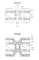
- a through hole 801 with a drum-shaped longitudinal cross-section is first formed in an insulating substrate 800, as shown in FIG. 8A .
- seed layer 802 made of metal is formed on the inner wall surface of this through hole 801, as shown in FIG. 8B .
- plated metal layer 803 is formed by filling the through hole with metal from the narrowest part (the part where the cross-sectional area is smallest) through electroplating.
- Patent Literature 1 Unexamined Japanese Patent Application KOKAI Publication No. 2004-311919
- thermosetting substrates in which resin (such as epoxy resin or the like) is impregnated with a reinforcing material such as glass cloth or the like in order to give mechanical strength are widely used as insulating substrates used in printed wiring boards.
- resin such as epoxy resin or the like
- a reinforcing material such as glass cloth or the like in order to give mechanical strength
- the reinforcing material could protrude from a wall surface of the resin.
- the hole diameter (L1) of the opening passing through the reinforcing material 810a and 810b is smaller than the diameter (L2) of the narrowest part of the through hole 801 passing through the resin, as shown in FIG. 9A .
- one reinforcing material 810a could be positioned not at the center of the substrate in the cross-sectional direction but between the center of the substrate and a first surface of the substrate, and the other reinforcing material 810b could be positioned between the center of the substrate and a second surface (the surface on the opposite side from the first surface) of the substrate, as shown in FIG. 9A .
- the printed wiring board according to the present invention is a printed wiring board comprising a substrate having a first surface and a second surface on the side opposite the first surface, and having a through hole comprising a first opening that is tapered from the first surface toward the second surface and a second opening that is tapered from the second surface toward the first surface; a first conductor circuit formed on the first surface of the substrate; a second conductor circuit formed on the second surface of the substrate; and a through hole conductor that fills the through hole and connects the first conductor circuit and the second conductor circuit; wherein the substrate is composed of a reinforcing material and a resin, and a portion of the reinforcing material protrudes into the through hole from the wall surface of the resin at the area where the first opening and the second opening intersect, and this protrusion of the reinforcing material encroaches into the through hole conductor.
- the method for manufacturing a printed wiring board according to the present invention is a method for manufacturing a printed wiring board including a procedure for preparing a substrate composed of a resin and a reinforcing material and having a first surface and a second surface on the side opposite the first surface; a procedure for forming a first opening that tapers from the first surface of the substrate toward the second surface; a procedure for forming a second opening that tapers from the second surface of the substrate toward the first surface, so that a through hole is formed comprising the first opening and the second opening; a procedure for forming a through hole conductor by filling the through hole with plating; and a procedure for forming a conductor circuit that connects the first surface and the second surface of the substrate by the through hole conductor; wherein in the procedure for forming the through hole, the through hole is formed such that the reinforcing material protrudes from the wall surface of the resin into the through hole at the intersection area where the first opening and the second opening intersect; and in the procedure for forming the through hole
- the present invention it is possible to suppress as much as possible occurrence of voids inside the through hole conductor in a printed wiring board and in addition to increase the bonding strength between the through hole conductor and the insulating substrate.
- a method for manufacturing a printed wiring board 1 (see FIG. 2 ) according to Embodiment 1 is described with reference to FIGS. 1A to 1I .
- a copper clad laminate in which copper foils 100 and 101 roughly 12 ⁇ m thick are laminated is prepared on both major surfaces of an insulating substrate 10 that is 0.1 mm to 0.6 mm thick.
- the thickness of the insulating substrate 10 is preferably 0.3 mm to 0.4 mm. When in this range, it is possible to secure strength in the substrate and it is easy to form a through hole shown in FIG. 1D using a laser.
- the insulating substrate 10 is composed of one piece of reinforcing material 14 and hardened resin 15. In this embodiment, the reinforcing material 14 is positioned substantially in the center of the insulating substrate 10 in the direction of thickness substantially parallel to both major surfaces of the insulating substrate 10.
- the thickness of the reinforcing material 14 is preferably 0.09 mm to 0.15 mm.
- a method for manufacturing a substrate in which the thickness of the insulating substrate is large with respect to the thickness of the reinforcing material will be simply explained. First, resin is impregnated with the reinforcing material and caused to dry. Next, resin is coated on both surfaces of the dried substrate. Following this, an insulating substrate with large thickness is obtained by the resin curing.
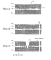
- an alignment mark 200 is formed passing through the copper clad laminate 10a (see FIG. 1B ).
- the alignment mark 200 can be formed by drill or laser.
- the alignment mark 200 is preferably a substantially straight through hole.
- the copper foil 100 and 101 of this copper clad laminate 10a is oxidized by a black oxide treatment.
- a laser is beamed at a prescribed spot on one of the major surfaces (a first surface) of the copper clad laminate 10a to form a first opening 201 (see FIG. 1C ).
- a carbon dioxide gas (CO 2 ) laser, Nd-YAG laser or excimer laser or the like can be used as the laser.
- the first opening 201 tapers from the first surface of the copper clad laminate 10a toward a second surface (a surface on the side opposite the first surface). Tapering from the first surface toward the second surface includes gradually narrowing from the first surface toward the second surface.
- the first opening 201 is formed with the alignment mark 200 as a reference.
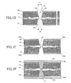
- a laser is beamed on a prescribed spot on the second surface of the copper clad laminate 10a to form a second opening 202 (see FIG. 1D ).
- the second opening 202 tapers from the second surface of the copper clad laminate 10a toward the first surface.
- the second opening 202 is also formed with the alignment mark 200 as a reference. Tapering from the second surface toward the first surface includes gradually narrowing from the second surface toward the first surface.
- the first opening 201 and the second opening 202 are formed with the same alignment mark 200 as a reference, so positioning with good accuracy is possible. Through this, the first opening 201 and the second opening 202 join at an area that is neither the first surface nor the second surface of the copper clad laminate 10a (inside the copper clad laminate 10a). As a result, a through hole (penetrating hole) 13a composed of the first opening 201 and the second opening 202 is formed, as shown in FIG. 1D .
- the copper clad laminate 10a has a reinforcing material 14.
- resin is more readily processed than reinforcing materials. Consequently, the diameter of the opening of the through hole readily becomes smallest at the position where the reinforcing material exists.
- the reinforcing material 14 is positioned substantially in the center of the copper clad laminate 10a, so it is easy for the opening diameter of the through hole 13a to become smallest at substantially the center of the copper clad laminate 10a.
- the diameter of the through hole 13a of this embodiment becomes smaller from the first surface of the copper clad laminate 10a toward the reinforcing material 14 positioned at substantially the center of the inside, and the opening diameter becomes larger from the position where it is smallest toward the second surface, as shown in FIG. 1D .
- the opening diameter of the through hole 13a does not change gradually but preferably changes significantly at the area where the reinforcing material 14 is positioned.
- portion (protrusion 140) of the reinforcing material 14 protrudes from the resin 15.
- the through hole 13a of this embodiment readily forms a shape having a difference in levels at substantially the center (the position where the reinforcing material 14 exists) of the copper clad laminate 10a (see FIG. 1D ).
- D2/D1 1/4 to 9/10.
- the length of protrusion 140 can be changed by adjusting the laser irradiation energy, the density thereof, the number of laser irradiations or the like, for example.
- a treatment for removing smears and the like remaining on the inner surface of the through hole 13a is accomplished.
- the besmear treatment is accomplished using the permanganate method. Specifically, first a conditioning (resin swelling) treatment is conducted on the copper clad laminate 10a of FIG. 1D . Following this the laminate is immersed for 5 to 30 minutes in a desmear treatment liquid of 40 to 80 g/l of permanganate at a temperature of 50 to 80° C. After this, the laminate is rinsed in water, immersed in a neutralizing solution, then rinsed in water and dried. As a result, smears are removed from the inner surface of the through hole 13a and a clean surface is exposed.
- a conditioning resin swelling
- a conditioning treatment and a soft-etching (also called micro-etching) treatment are conducted on the copper clad laminate 10a.
- the laminate is immersed in a catalyzing liquid containing alkaline Pd complex ions, and a catalyst for starting non-electroplating (such as non-electroplated copper and non-electroplated nickel) are adsorbed to both major surfaces of the copper clad laminate 10a and the inner surface of the through hole 13a.
- non-electroplated film for example, non-electroplated copper film or non-electroplated nickel film
- non-electroplated film 102a is also deposited on protrusion 140 protruding to the inside of the through hole 13a from the wall surface of the resin 15 in the center of the through hole 13a.
- an electroplating treatment for example, an electrolytic copper plating treatment or an electrolytic nickel treatment
- non-electroplated film 102 as a seed layer
- the through hole 13a is filled with plating (for example, electroplating such as electrolytic copper plating or electrolytic nickel or the like) and a through hole conductor (composed of non-electroplated film and electroplated film on non-electroplated film) 13 is formed (see FIG. 1F ).
- electroplated film 102c is formed on non-electroplated film 102a on both major surfaces of the substrate, and for example plated film 102b composed of non-electroplated film 102a and electroplated film 102c is formed.
- protrusion 140 that protrudes to the inside of the through hole 13a from the resin 15, as shown in FIG. 1D . Accordingly, at the area where protrusion 140 is formed, the opening diameter of the through hole 13a readily becomes a minimum.
- non-electroplated film 102a is formed on the surface (that is to say, the inner wall of the through hole 13a) of protrusion 140 and the resin 15 exposed by the through hole 13a. When filling the through hole 13a with electroplating, this non-electroplated film 102a functions as a seed layer. In this embodiment, during electroplating the plating readily fills the space formed by the inner walls of protrusion 140 first (see FIG. 1G ). After this, the through hole 13a is filled with plating from the area where protrusion 140 exists toward the first surface and the second surface of the substrate.
- the through hole 13a is filled with plating from the narrowest area (the area where protrusion 140 exists).
- a copper clad laminate 10a containing a single sheet of reinforcing material 14 is used, so protrusion 140 protruding from the inner walls of the through hole 13a is concentrated in one area (the center of the substrate). Accordingly, it is difficult for multiple areas in the through hole 13a to be simultaneously closed up with plating.
- the volume of the space formed by the inner walls of protrusion 140 is small, it is difficult for voids to occur at the area having the smallest opening diameter (the space formed by the inner walls of protrusion 140). Consequently, it is easy for the through hole 13a to be filled with plating from the center of the substrate toward the first surface and the second surface of the substrate.
- the reinforcing material 14 is positioned substantially in the center of the substrate and protrusion 140 is also positioned substantially in the center of the substrate. Consequently, filling with plating progresses substantially simultaneously from the center of the substrate toward the first surface and the second surface. As a result, it is easy for the thickness of plating film 102b formed on the first surface and the second surface of the substrate to become thin. Through this, processing with subsequent processes such as etching becomes easier, making it easy to make conductor circuits finer.
- etching resists 103 and 104 for protecting conductive patterns that are to remain are formed on the surfaces of plating film (for example, copper plating film) 102b, as shown in FIG. 1H .
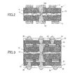
- plating film 102b exposed from the etching resists 103 and 104 and copper foils 100 and 101 are etched to form conductor circuits 11 and 12 (see FIG. 1I ). After etching, etching resists 103 and 104 are peeled off to obtain the printed wiring board 1 shown in FIG. 2 .
- the printed wiring board 1 of this embodiment manufactured as described above has the below-described excellent characteristics in addition to the above-described characteristic that the occurrence of voids inside the through hole conductor 13 is suppressed as much as possible.
- the through hole conductor 13 is formed in a tapered shape toward the center of the printed wiring board 1, and consequently the mechanical bonding strength with the insulating substrate 10 is high.
- protrusion 140 part of the reinforcing material 14 protruding from the resin 15 encroaches into the center of the through hole conductor 13, it is possible to effectively ease the pulling stress in the vertical direction of the through hole conductor 13. Accordingly, the bonding strength between the insulating substrate 10 and the through hole conductor 13 is further increased.
- FIG. 3 shows one example of a build-up multi-layer printed wiring board using the printed wiring board 1 of FIG. 2 as the core substrate. The process for manufacturing this build-up multi-layer printed wiring board is briefly explained below.
- interlayer resin insulating layers 30 and 31 are formed on the first surface and the second surface, respectively of the printed wiring board 1 of FIG. 2 .
- openings reaching conductor circuits 11 and 12 formed on the printed wiring board 1 are formed in interlayer resin insulating layers 30 and 31.
- conductor circuits 32 and 33 are formed on interlayer resin insulating layers 30 and 31, respectively.
- via conductors 34 and 35 are formed simultaneously in the openings of interlayer resin insulating layers 30 and 31, respectively.
- conductor circuit 11 and conductor circuit 32 are electrically connected by via conductor 34
- conductor circuit 12 and conductor circuit 33 are electrically connected by via conductor 35.
- a liquid or dry film photosensitive resist (solder resist) is coated or laminated on both major surfaces of the substrate.
- Thermosetting solder resist may also be used.
- solder resist layers 36 and 37 having openings for exposing parts that are solder pads of conductor circuits 32 and 33 are formed.
- the openings having solder resist layers 36 and 37 may be openings exposing part of the top surfaces of via conductors 34 and 35. In addition, these may also be openings exposing the entire top surfaces of via conductors 34 and 35 and parts of conductor circuits 32 and 33 directly connected to the conductors 34 and 35.
- solder paste is imprinted on the solder pads and solder bumps 38 and 39 are formed by accomplishing reflow.
- the build-up multi-layer printed wiring board of FIG. 3 formed in this manner is electrically connected to a daughter board or the like or to electronic components such as an IC chip or the like via solder bumps 38 and 39.
- the copper clad laminate 10a used has a single sheet of reinforcing material 14, and this reinforcing material 14 is positioned substantially in the center of the insulating substrate 10.
- protrusion 140 of the reinforcing material 14 protruding from the inner wall encroaches into the through hole conductor 13.
- the positioning condition of the reinforcing material 14 and the shape of the through hole conductor 13 and so forth are not limited. All that is necessary is for protrusion 140 of the reinforcing material 14 to exist at the intersection of the first opening 201 and the second opening 202. By having the reinforcing material 14 exist at the intersection of the first opening 201 and the second opening 202, it is possible to make the diameter of the opening of the intersection the minimum diameter of the through hole 13a. In addition, the location where the opening diameter is smallest readily becomes a single location in the cross-sectional direction of the through hole 13a.
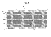
- FIG. 4 is a cross-sectional view of a printed wiring board 40 according to Embodiment 2.
- the insulating substrate 10 is composed of three sheets of reinforcing material 14a, 14b and 14c and a hardened resin 15.
- the reinforcing material 14b is positioned substantially at the center of the insulating substrate 10.
- the reinforcing material 14a is positioned between the center and a first surface of the insulating substrate 10.
- the reinforcing material 14c is positioned between the center and a second surface of the insulating substrate 10.
- portion of the reinforcing material 14b (protrusion 140) encroaches into each through hole conductor 13.
- a copper clad laminate 10a is prepared on which copper foils 100 and 101 having a thickness of 12 ⁇ m are laminated on both major surfaces of the insulating substrate 10 having a thickness of approximately 0.4 mm.
- the insulating substrate 10 is a substrate in which three sheets of reinforcing materials 14a to 14c are immersed in resin and the resin is hardened. These three sheets of reinforcing material 14a to 14c are each positioned substantially parallel to both major surfaces of the copper clad laminate 10a.
- an alignment mark (unrepresented) passing through the copper clad laminate 10a is formed. Furthermore, copper foils 100 and 101 of this copper clad laminate 10a are oxidized by a black oxide treatment.
- through holes 13a composed of a first opening and a second opening are formed at prescribed locations in the copper clad laminate 10a (see FIG. 5B ). The first opening tapers from the first surface of the copper clad laminate 10a toward the second surface. The second opening tapers from the second surface of the copper clad laminate 10a toward the first surface.
- the method for forming through holes 13a is the same as that of Embodiment 1.
- the reinforcing material 14b exists at the intersection of the first and second openings.
- portion (protrusion) of the reinforcing material 14b exists at the intersection of the first and second openings.
- the opening diameter of the through hole 13a is smallest at the intersection of the first and second openings.
- the reinforcing materials 14a and 14c may also have protrusions protruding into the through hole 13a from the resin 5.
- the opening diameter (r1) of the opening formed in the reinforcing material 14a is larger than the opening diameter (r2) of the opening formed in the reinforcing material 14b.
- the opening diameter (r3) of the opening formed in the reinforcing material 14c is also larger than r2.
- the thickness of the reinforcing material 14b may be thicker than the thicknesses of the reinforcing materials 14a and 14c positioned above and below such.
- the thickness of the reinforcing material 14b is thicker than the thickness of the reinforcing materials 14a and 14c (that is to say, the thickness of the reinforcing materials 14a and 14c is thinner than the thickness of the reinforcing material 14b).
- the thickness of the reinforcing material 14b is preferably 0.12 to 0.15 mm
- the thickness of the reinforcing materials 14a to 14c is preferably 0.09 to 0.12 mm.
- the difference in thicknesses between the reinforcing material 14b and the reinforcing materials 14a and 14c is preferably on the order of 0.015 to 0.05 mm.
- non-electroplated film 102a is formed on both major surfaces of the copper clad laminate 10a and inner walls of through holes 13a (see FIG. 5C ). Through this, the spaces formed by the inner walls of the reinforcing material 14b are filled by non-electroplated film 102a.
- an electroplating treatment is accomplished to form plating film 102b and through hole conductors 13 (see FIG. 5D ). After this, etching resists 103 and 104 for protecting conductor patterns that should remain are formed on the surface of plating film 102b, as shown in FIG. 5E .
- the printed wiring board 40 of this embodiment manufactured as described above has increased substrate strength because three sheets of reinforcing material 14a to 14c are used.
- the number of reinforcing materials is an odd number similar to the printed wiring board 1 of Embodiment 1, it is easy to position the reinforcing material (14b) in the center of the insulating substrate 10.
- the diameter of the through hole 13a readily becomes smallest at the center of the insulating substrate 10.
- the reinforcing material 14b in the center of the insulating substrate 10. the balance is good in the direction of thickness of the printed wiring board 40, so curving of the substrate can be suppressed.
- references numbers 30 and 31 indicate inter-layer resin insulating layers
- reference numbers 32 and 33 indicate conductor circuits
- reference numbers 34 and 35 indicate via conductors
- reference numbers 36 and 37 indicate solder resist layers
- reference numbers 38 and 39 indicate solder bumps.
- FIGS. 7A to 7D are summary cross-sections showing the state of essential parts after formation of non-electroplated films 102a in other embodiments.
- the insulating substrate 10 contains three sheets of reinforcing material 70a to 70c, and the thickness of each reinforcing material 70 is the same (for example, 100 ⁇ m).
- the insulating substrate 10 contains four (that is to say, an even number of) sheets of reinforcing material 71a to 71d, and the thickness of each reinforcing material 71 is the same (for example, 100 ⁇ m).
- the smallest diameter of the through hole in FIGS. 7A to 7D is at the intersection of the first and second openings, and in this area, reinforcing material protrudes into the through hole.
- the area where the opening diameter of the through hole is smallest is not positioned at substantially the center of the substrate.
- the intersection is positioned between the center of the substrate and the first surface.
- the intersection is positioned between the center of the substrate and the second surface.
- the printed wiring board having the intersection between the center of the substrate and the first surface or the second surface of the substrate can be used preferably as the core substrate in the build-up multilayer printed wiring board shown in FIG. 3 or FIG. 6 . That is because the stress added to the curved portions of through hole conductors is reduced. Moreover, in this case it is preferable for the number of sheets of reinforcing material to be an even number.
- the art of the present invention can be broadly applied to printed wiring boards in which through holes are filled with metal.
Landscapes
- Engineering & Computer Science (AREA)
- Manufacturing & Machinery (AREA)
- Microelectronics & Electronic Packaging (AREA)
- Physics & Mathematics (AREA)
- Optics & Photonics (AREA)
- Printing Elements For Providing Electric Connections Between Printed Circuits (AREA)
- Production Of Multi-Layered Print Wiring Board (AREA)
Abstract
Description
- The present invention relates to a printed wiring board provided with a through hole passing through an insulating substrate, and a method for manufacturing such, and in particular, to a printed wiring board in which the through hole is filled with metal, and a method for manufacturing such.
- A method for filling the inside of a through hole with metal through plating from the perspective of improving electrical properties has been known from before.
- For example,
Patent Literature 1 discloses technology (a through hole fill method) for preventing the occurrence of voids or the like by making the shape of the through hole a drum shape. The drum-shaped through hole is a through hole made up of a first opening that is tapered from a first surface of the substrate toward a second surface of the substrate, and a second opening that is tapered from the second surface of the substrate toward the first surface of the substrate. The first opening and the second opening join inside the substrate. - With this through hole fill method, a
through hole 801 with a drum-shaped longitudinal cross-section is first formed in aninsulating substrate 800, as shown inFIG. 8A . Next,seed layer 802 made of metal is formed on the inner wall surface of this throughhole 801, as shown inFIG. 8B . From there,plated metal layer 803 is formed by filling the through hole with metal from the narrowest part (the part where the cross-sectional area is smallest) through electroplating. - Patent Literature 1: Unexamined Japanese Patent Application KOKAI Publication No.
2004-311919 - However, thermosetting substrates in which resin (such as epoxy resin or the like) is impregnated with a reinforcing material such as glass cloth or the like in order to give mechanical strength are widely used as insulating substrates used in printed wiring boards. When a through hole is formed in a substrate including this manner of reinforcing material on the basis of the technology disclosed in
Patent Literature 1, there is a possibility that the reinforcing material could protrude from a wall surface of the resin. In such instances, a case could conceivably occur in which the hole diameter (L1) of the opening passing through thereinforcing material hole 801 passing through the resin, as shown inFIG. 9A . - In general, in a substrate composed of resin and two pieces of reinforcing material, it is conceivable that one reinforcing
material 810a could be positioned not at the center of the substrate in the cross-sectional direction but between the center of the substrate and a first surface of the substrate, and the other reinforcingmaterial 810b could be positioned between the center of the substrate and a second surface (the surface on the opposite side from the first surface) of the substrate, as shown inFIG. 9A . When the through hole of such a substrate is filled by plating (electroplating), it is conceivable that the part passing through thereinforcing materials hole 801 passing through the substrate. In such a case, there are concerns that avoid 811 could occur in the narrowest part of the throughhole 801 passing through the resin, as shown inFIG. 9B . - It is an object of the present invention to provide a printed wiring board that suppresses as much as possible occurrence of voids inside the through hole conductor and also increases bonding strength between the through hole conductor and the insulating substrate, and a method for manufacturing such.
- The printed wiring board according to the present invention is a printed wiring board comprising a substrate having a first surface and a second surface on the side opposite the first surface, and having a through hole comprising a first opening that is tapered from the first surface toward the second surface and a second opening that is tapered from the second surface toward the first surface; a first conductor circuit formed on the first surface of the substrate; a second conductor circuit formed on the second surface of the substrate; and a through hole conductor that fills the through hole and connects the first conductor circuit and the second conductor circuit; wherein the substrate is composed of a reinforcing material and a resin, and a portion of the reinforcing material protrudes into the through hole from the wall surface of the resin at the area where the first opening and the second opening intersect, and this protrusion of the reinforcing material encroaches into the through hole conductor.
- In addition, the method for manufacturing a printed wiring board according to the present invention is a method for manufacturing a printed wiring board including a procedure for preparing a substrate composed of a resin and a reinforcing material and having a first surface and a second surface on the side opposite the first surface; a procedure for forming a first opening that tapers from the first surface of the substrate toward the second surface; a procedure for forming a second opening that tapers from the second surface of the substrate toward the first surface, so that a through hole is formed comprising the first opening and the second opening; a procedure for forming a through hole conductor by filling the through hole with plating; and a procedure for forming a conductor circuit that connects the first surface and the second surface of the substrate by the through hole conductor; wherein in the procedure for forming the through hole, the through hole is formed such that the reinforcing material protrudes from the wall surface of the resin into the through hole at the intersection area where the first opening and the second opening intersect; and in the procedure for forming the through hole conductor, the through hole is filled with plating from the intersection area toward the first surface and the second surface of the substrate.
- With the present invention, it is possible to suppress as much as possible occurrence of voids inside the through hole conductor in a printed wiring board and in addition to increase the bonding strength between the through hole conductor and the insulating substrate.
-
-
FIG. 1A is a cross-section of a copper clad laminate used inEmbodiment 1 of the present invention. -
FIG. 1B is a cross-section showing the state when an alignment mark is formed in the substrate ofFIG. 1A . -
FIG. 1C is a cross-section showing the state when a first opening is formed in a first surface of the substrate ofFIG. 1B . -
FIG. 1D is a cross-section showing the state when a second opening is formed in a second surface of the substrate ofFIG. 1C . -
FIG. 1E is a cross-section showing the state after non-electroplating has been conducted on the substrate ofFIG. 1D . -
FIG. 1F is a cross-section showing the state after electroplating has been conducted on the substrate ofFIG. 1E . -
FIG. 1G is a cross-section showing the state with plating filling the part where a protrusion exists, when electroplating. -
FIG. 1H is a cross-section showing the state when etching resists are formed on the substrate ofFIG. 1F . -
FIG. 1I is a cross-section showing the state after etching has been conducted on the substrate ofFIG. 1H . -
FIG. 2 is a cross-section showing of a printed wiring board according to Embodiment 1 of the present invention. -
FIG. 3 is a cross-section of a build-up multi-layer printed wiring board using the printed wiring board ofFIG. 2 . -
FIG. 4 is a cross-section of a printed wiring board according to Embodiment 2 of the present invention. -
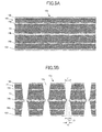
FIG. 5A is a cross-section of a copper clad laminate used in Embodiment 2 of the present invention. -
FIG. 5B is a cross-section showing the state after through holes have been formed in the substrate ofFIG. 5A . -
FIG. 5C is a cross-section showing the state after non-electroplating has been conducted on the substrate ofFIG. 5B . -
FIG. 5D is a cross-section showing the state after electroplating has been conducted on the substrate ofFIG. 5C . -
FIG. 5E is a cross-section showing the state when an etching resists are formed on the substrate ofFIG. 5D . -
FIG. 5F is a cross-section showing the state after etching has been conducted on the substrate ofFIG. 5E . -
FIG. 6 is a cross-section of a build-up multi-layer printed wiring board using the printed wiring board ofFIG. 4 . -
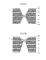
FIG. 7A is a cross-section showing the state of an essential part (pattern 1) after a non-electroplated film has been formed in another embodiment. -
FIG. 7B is a cross-section showing the state of an essential part (pattern 2) after a non-electroplated film has been formed in another embodiment. -
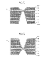
FIG. 7C is a cross-section showing the state of an essential part (pattern 3) after a non-electroplated film has been formed in another embodiment. -
FIG. 7D is a cross-section showing the state of an essential part (pattern 4) after a non-electroplated film has been formed in another embodiment. -
FIG. 8A is a cross-section showing a drum-shaped through hole in an example of prior art technology. -
FIG. 8B is a cross-section showing the state when the through hole ofFIG. 8A is filled with metal. -
FIG. 9A is a cross-section showing the state after the through hole has been formed, and is a drawing used to explain one conceivable problem the prior art technology possesses. -
FIG. 9B is a cross-section showing the state when the through hole ofFIG. 9A is filled with metal. - The printed wiring board and method for manufacturing same according to the preferred embodiments of the present invention are described below with reference to the drawings.
- A method for manufacturing a printed wiring board 1 (see
FIG. 2 ) according toEmbodiment 1 is described with reference toFIGS. 1A to 1I . - First, as shown in
FIG. 1A , a copper clad laminate in which copper foils 100 and 101 roughly 12 µm thick are laminated is prepared on both major surfaces of an insulatingsubstrate 10 that is 0.1 mm to 0.6 mm thick. The thickness of the insulatingsubstrate 10 is preferably 0.3 mm to 0.4 mm. When in this range, it is possible to secure strength in the substrate and it is easy to form a through hole shown inFIG. 1D using a laser. The insulatingsubstrate 10 is composed of one piece of reinforcingmaterial 14 andhardened resin 15. In this embodiment, the reinforcingmaterial 14 is positioned substantially in the center of the insulatingsubstrate 10 in the direction of thickness substantially parallel to both major surfaces of the insulatingsubstrate 10. - As a reinforcing material, it is possible to utilize glass cloth, glass nonwoven cloth or aramid nonwoven cloth. Of these, from the perspective of strength it is preferable to use a sheet-like reinforcing material composed of glass cloth, and the thickness of the reinforcing
material 14 is preferably 0.09 mm to 0.15 mm. - A method for manufacturing a substrate in which the thickness of the insulating substrate is large with respect to the thickness of the reinforcing material will be simply explained. First, resin is impregnated with the reinforcing material and caused to dry. Next, resin is coated on both surfaces of the dried substrate. Following this, an insulating substrate with large thickness is obtained by the resin curing.
- Next, an
alignment mark 200 is formed passing through the copper cladlaminate 10a (seeFIG. 1B ). Thealignment mark 200 can be formed by drill or laser. Thealignment mark 200 is preferably a substantially straight through hole. Next, thecopper foil laminate 10a is oxidized by a black oxide treatment. - Next, a laser is beamed at a prescribed spot on one of the major surfaces (a first surface) of the copper clad
laminate 10a to form a first opening 201 (seeFIG. 1C ). As the laser, a carbon dioxide gas (CO2) laser, Nd-YAG laser or excimer laser or the like can be used. Thefirst opening 201 tapers from the first surface of the copper cladlaminate 10a toward a second surface (a surface on the side opposite the first surface). Tapering from the first surface toward the second surface includes gradually narrowing from the first surface toward the second surface. Thefirst opening 201 is formed with thealignment mark 200 as a reference. - Following this, a laser is beamed on a prescribed spot on the second surface of the copper clad
laminate 10a to form a second opening 202 (seeFIG. 1D ). Thesecond opening 202 tapers from the second surface of the copper cladlaminate 10a toward the first surface. Thesecond opening 202 is also formed with thealignment mark 200 as a reference. Tapering from the second surface toward the first surface includes gradually narrowing from the second surface toward the first surface. - The
first opening 201 and thesecond opening 202 are formed with thesame alignment mark 200 as a reference, so positioning with good accuracy is possible. Through this, thefirst opening 201 and thesecond opening 202 join at an area that is neither the first surface nor the second surface of the copper cladlaminate 10a (inside the copper cladlaminate 10a). As a result, a through hole (penetrating hole) 13a composed of thefirst opening 201 and thesecond opening 202 is formed, as shown inFIG. 1D . - As described above, the copper clad
laminate 10a has a reinforcingmaterial 14. Normally, when comparing resin and reinforcing materials, resin is more readily processed than reinforcing materials. Consequently, the diameter of the opening of the through hole readily becomes smallest at the position where the reinforcing material exists. In addition, in the present embodiment, the reinforcingmaterial 14 is positioned substantially in the center of the copper cladlaminate 10a, so it is easy for the opening diameter of the throughhole 13a to become smallest at substantially the center of the copper cladlaminate 10a. - As a result, the diameter of the through
hole 13a of this embodiment becomes smaller from the first surface of the copper cladlaminate 10a toward the reinforcingmaterial 14 positioned at substantially the center of the inside, and the opening diameter becomes larger from the position where it is smallest toward the second surface, as shown inFIG. 1D . In addition, the opening diameter of the throughhole 13a does not change gradually but preferably changes significantly at the area where the reinforcingmaterial 14 is positioned. In addition, at the position where the opening diameter of the throughhole 13a is the smallest, portion (protrusion 140) of the reinforcingmaterial 14 protrudes from theresin 15. - As noted above, in this embodiment, there is
protrusion 140 of reinforcingmaterial 14 protruding in the throughhole 13a at substantially the center of the copper cladlaminate 10a. Consequently, the throughhole 13a of this embodiment readily forms a shape having a difference in levels at substantially the center (the position where the reinforcingmaterial 14 exists) of the copper cladlaminate 10a (seeFIG. 1D ). - As shown in
FIG. 1D , the minimum diameter of the throughhole 13a (the opening diameter D2 formed by the reinforcing material 14) and the opening diameter D1 formed by theresin 15 at that position are preferably related such that D2/D1 = 1/4 to 9/10. When D2/D1 is in this range, it is easy to fill the inside of the throughhole 13a by plating. - The length of
protrusion 140 can be changed by adjusting the laser irradiation energy, the density thereof, the number of laser irradiations or the like, for example. - Next, a treatment (desmear treatment) for removing smears and the like remaining on the inner surface of the through
hole 13a is accomplished. The besmear treatment is accomplished using the permanganate method. Specifically, first a conditioning (resin swelling) treatment is conducted on the copper cladlaminate 10a ofFIG. 1D . Following this the laminate is immersed for 5 to 30 minutes in a desmear treatment liquid of 40 to 80 g/l of permanganate at a temperature of 50 to 80° C. After this, the laminate is rinsed in water, immersed in a neutralizing solution, then rinsed in water and dried. As a result, smears are removed from the inner surface of the throughhole 13a and a clean surface is exposed. - Following the desmear treatment, a conditioning treatment and a soft-etching (also called micro-etching) treatment are conducted on the copper clad
laminate 10a. After this, the laminate is immersed in a catalyzing liquid containing alkaline Pd complex ions, and a catalyst for starting non-electroplating (such as non-electroplated copper and non-electroplated nickel) are adsorbed to both major surfaces of the copper cladlaminate 10a and the inner surface of the throughhole 13a. - Furthermore, when the copper clad
laminate 10a with this catalyst adsorbed is immersed in a non-electroplating liquid, a substrate is obtained in which non-electroplated film (for example, non-electroplated copper film or non-electroplated nickel film) 102a is formed on both major surfaces and the inner surface of the throughhole 13a, as shown inFIG. 1E . In addition, at thistime non-electroplated film 102a is also deposited onprotrusion 140 protruding to the inside of the throughhole 13a from the wall surface of theresin 15 in the center of the throughhole 13a. - Next, an electroplating treatment (for example, an electrolytic copper plating treatment or an electrolytic nickel treatment) is accomplished with non-electroplated film 102 as a seed layer, the through
hole 13a is filled with plating (for example, electroplating such as electrolytic copper plating or electrolytic nickel or the like) and a through hole conductor (composed of non-electroplated film and electroplated film on non-electroplated film) 13 is formed (seeFIG. 1F ). In addition, at this time electroplatedfilm 102c is formed onnon-electroplated film 102a on both major surfaces of the substrate, and for example platedfilm 102b composed ofnon-electroplated film 102a and electroplatedfilm 102c is formed. - In this embodiment, there is
protrusion 140 that protrudes to the inside of the throughhole 13a from theresin 15, as shown inFIG. 1D . Accordingly, at the area whereprotrusion 140 is formed, the opening diameter of the throughhole 13a readily becomes a minimum. In addition, as shown inFIG. 1E ,non-electroplated film 102a is formed on the surface (that is to say, the inner wall of the throughhole 13a) ofprotrusion 140 and theresin 15 exposed by the throughhole 13a. When filling the throughhole 13a with electroplating, thisnon-electroplated film 102a functions as a seed layer. In this embodiment, during electroplating the plating readily fills the space formed by the inner walls ofprotrusion 140 first (seeFIG. 1G ). After this, the throughhole 13a is filled with plating from the area whereprotrusion 140 exists toward the first surface and the second surface of the substrate. - As described above, because of the existence of
protrusion 140 protruding from the inner walls of the throughhole 13a, the throughhole 13a is filled with plating from the narrowest area (the area whereprotrusion 140 exists). In addition, with this embodiment, a copper cladlaminate 10a containing a single sheet of reinforcingmaterial 14 is used, soprotrusion 140 protruding from the inner walls of the throughhole 13a is concentrated in one area (the center of the substrate). Accordingly, it is difficult for multiple areas in the throughhole 13a to be simultaneously closed up with plating. In addition, because the volume of the space formed by the inner walls ofprotrusion 140 is small, it is difficult for voids to occur at the area having the smallest opening diameter (the space formed by the inner walls of protrusion 140). Consequently, it is easy for the throughhole 13a to be filled with plating from the center of the substrate toward the first surface and the second surface of the substrate. - In the case of this embodiment, the reinforcing
material 14 is positioned substantially in the center of the substrate andprotrusion 140 is also positioned substantially in the center of the substrate. Consequently, filling with plating progresses substantially simultaneously from the center of the substrate toward the first surface and the second surface. As a result, it is easy for the thickness of platingfilm 102b formed on the first surface and the second surface of the substrate to become thin. Through this, processing with subsequent processes such as etching becomes easier, making it easy to make conductor circuits finer. - Next, etching resists 103 and 104 for protecting conductive patterns that are to remain are formed on the surfaces of plating film (for example, copper plating film) 102b, as shown in
FIG. 1H . - Furthermore, plating
film 102b exposed from the etching resists 103 and 104 and copper foils 100 and 101 are etched to formconductor circuits 11 and 12 (seeFIG. 1I ). After etching, etching resists 103 and 104 are peeled off to obtain the printedwiring board 1 shown inFIG. 2 . - The printed
wiring board 1 of this embodiment manufactured as described above has the below-described excellent characteristics in addition to the above-described characteristic that the occurrence of voids inside the throughhole conductor 13 is suppressed as much as possible. - The through
hole conductor 13 is formed in a tapered shape toward the center of the printedwiring board 1, and consequently the mechanical bonding strength with the insulatingsubstrate 10 is high. - Because protrusion 140 (part of the reinforcing material 14) protruding from the
resin 15 encroaches into the center of the throughhole conductor 13, it is possible to effectively ease the pulling stress in the vertical direction of the throughhole conductor 13. Accordingly, the bonding strength between the insulatingsubstrate 10 and the throughhole conductor 13 is further increased. - This kind of printed
wiring board 1 is used as the core substrate of a multi-layer printed wiring board.FIG. 3 shows one example of a build-up multi-layer printed wiring board using the printedwiring board 1 ofFIG. 2 as the core substrate. The process for manufacturing this build-up multi-layer printed wiring board is briefly explained below. - First, interlayer
resin insulating layers wiring board 1 ofFIG. 2 . Following this, openings reachingconductor circuits wiring board 1 are formed in interlayerresin insulating layers conductor circuits resin insulating layers conductors resin insulating layers conductor circuit 11 andconductor circuit 32 are electrically connected by viaconductor 34, andconductor circuit 12 andconductor circuit 33 are electrically connected by viaconductor 35. - Next, a liquid or dry film photosensitive resist (solder resist) is coated or laminated on both major surfaces of the substrate. Thermosetting solder resist may also be used.
- Furthermore, a mask film in which a prescribed pattern is formed is adhered to the surface of the photosensitive resist, this is exposed to ultraviolet rays and then developed by an alkaline solution. As a result, solder resist
layers conductor circuits - The openings having solder resist
layers conductors conductors conductor circuits conductors - Next, solder paste is imprinted on the solder pads and solder bumps 38 and 39 are formed by accomplishing reflow. The build-up multi-layer printed wiring board of
FIG. 3 formed in this manner is electrically connected to a daughter board or the like or to electronic components such as an IC chip or the like via solder bumps 38 and 39. - In this embodiment, the copper clad
laminate 10a used has a single sheet of reinforcingmaterial 14, and this reinforcingmaterial 14 is positioned substantially in the center of the insulatingsubstrate 10. In addition, in the center region of the throughhole conductor 13,protrusion 140 of the reinforcingmaterial 14 protruding from the inner wall, encroaches into the throughhole conductor 13. - However, the positioning condition of the reinforcing
material 14 and the shape of the throughhole conductor 13 and so forth are not limited. All that is necessary is forprotrusion 140 of the reinforcingmaterial 14 to exist at the intersection of thefirst opening 201 and thesecond opening 202. By having the reinforcingmaterial 14 exist at the intersection of thefirst opening 201 and thesecond opening 202, it is possible to make the diameter of the opening of the intersection the minimum diameter of the throughhole 13a. In addition, the location where the opening diameter is smallest readily becomes a single location in the cross-sectional direction of the throughhole 13a. -
FIG. 4 is a cross-sectional view of a printedwiring board 40 according to Embodiment 2. In this printedwiring board 40, the insulatingsubstrate 10 is composed of three sheets of reinforcingmaterial hardened resin 15. The reinforcingmaterial 14b is positioned substantially at the center of the insulatingsubstrate 10. The reinforcingmaterial 14a is positioned between the center and a first surface of the insulatingsubstrate 10. The reinforcingmaterial 14c is positioned between the center and a second surface of the insulatingsubstrate 10. In addition, portion of the reinforcingmaterial 14b (protrusion 140) encroaches into each throughhole conductor 13. - The method for manufacturing this printed
wiring board 40 is described below with reference toFIGS. 5A to 5F . First, as shown inFIG. 5A , a copper cladlaminate 10a is prepared on which copper foils 100 and 101 having a thickness of 12 µm are laminated on both major surfaces of the insulatingsubstrate 10 having a thickness of approximately 0.4 mm. In this embodiment, the insulatingsubstrate 10 is a substrate in which three sheets of reinforcingmaterials 14a to 14c are immersed in resin and the resin is hardened. These three sheets of reinforcingmaterial 14a to 14c are each positioned substantially parallel to both major surfaces of the copper cladlaminate 10a. - Next, an alignment mark (unrepresented) passing through the copper clad
laminate 10a is formed. Furthermore, copper foils 100 and 101 of this copper cladlaminate 10a are oxidized by a black oxide treatment. Next, throughholes 13a composed of a first opening and a second opening are formed at prescribed locations in the copper cladlaminate 10a (seeFIG. 5B ). The first opening tapers from the first surface of the copper cladlaminate 10a toward the second surface. The second opening tapers from the second surface of the copper cladlaminate 10a toward the first surface. The method for forming throughholes 13a is the same as that ofEmbodiment 1. - With this embodiment, the reinforcing
material 14b exists at the intersection of the first and second openings. In other words, portion (protrusion) of the reinforcingmaterial 14b exists at the intersection of the first and second openings. In addition, the opening diameter of the throughhole 13a is smallest at the intersection of the first and second openings. The reinforcingmaterials hole 13a from the resin 5. However, the opening diameter (r1) of the opening formed in the reinforcingmaterial 14a is larger than the opening diameter (r2) of the opening formed in the reinforcingmaterial 14b. In addition, the opening diameter (r3) of the opening formed in the reinforcingmaterial 14c is also larger than r2. - As a method for forming through holes satisfying r1 > r2 and r3 > r2, for example, a method for forming the first and second openings through laser light with higher energy density in the center than at the perimeter can be cited. In addition, by changing the thicknesses of reinforcing materials, it is possible to form through holes satisfying r1 > r2 and r3 > r2. Specifically, the thickness of the reinforcing
material 14b may be thicker than the thicknesses of the reinforcingmaterials material 14b is thicker than the thickness of the reinforcingmaterials materials material 14b). In this case, the thickness of the reinforcingmaterial 14b is preferably 0.12 to 0.15 mm, and the thickness of the reinforcingmaterials 14a to 14c is preferably 0.09 to 0.12 mm. In addition, the difference in thicknesses between the reinforcingmaterial 14b and the reinforcingmaterials - After formation of through
holes 13a,non-electroplated film 102a is formed on both major surfaces of the copper cladlaminate 10a and inner walls of throughholes 13a (seeFIG. 5C ). Through this, the spaces formed by the inner walls of the reinforcingmaterial 14b are filled bynon-electroplated film 102a. After formation ofnon-electroplated film 102a, an electroplating treatment is accomplished to form platingfilm 102b and through hole conductors 13 (seeFIG. 5D ). After this, etching resists 103 and 104 for protecting conductor patterns that should remain are formed on the surface of platingfilm 102b, as shown inFIG. 5E . - Furthermore, plating
film 102b and copper foils 100 and 101 exposed from etching resists 103 and 104 and are etched to formconductor circuits 11 and 12 (seeFIG. 5F ). After etching, by conducting a step to remove the etching resists, the printedwiring board 40 shown inFIG. 4 is obtained. - The printed
wiring board 40 of this embodiment manufactured as described above has increased substrate strength because three sheets of reinforcingmaterial 14a to 14c are used. In addition, because the number of reinforcing materials is an odd number similar to the printedwiring board 1 ofEmbodiment 1, it is easy to position the reinforcing material (14b) in the center of the insulatingsubstrate 10. As a result, the diameter of the throughhole 13a readily becomes smallest at the center of the insulatingsubstrate 10. Furthermore, by positioning the reinforcingmaterial 14b in the center of the insulatingsubstrate 10. the balance is good in the direction of thickness of the printedwiring board 40, so curving of the substrate can be suppressed. - In addition, a multi-layer printed wiring board such as that shown in
FIG. 6 can be obtained by forming build-up layers using the printedwiring board 40 as the core substrate. InFIG. 6 ,references numbers reference numbers reference numbers reference numbers reference numbers - The present invention is not limited by the above-described embodiments, for various alterations are possible without departing from the principles of the present invention
-
FIGS. 7A to 7D are summary cross-sections showing the state of essential parts after formation ofnon-electroplated films 102a in other embodiments. InFIGS. 7A and 7B , the insulatingsubstrate 10 contains three sheets of reinforcingmaterial 70a to 70c, and the thickness of each reinforcing material 70 is the same (for example, 100 µm). - In
FIGS. 7C and 7D , the insulatingsubstrate 10 contains four (that is to say, an even number of) sheets of reinforcingmaterial 71a to 71d, and the thickness of each reinforcing material 71 is the same (for example, 100 µm). - The smallest diameter of the through hole in
FIGS. 7A to 7D is at the intersection of the first and second openings, and in this area, reinforcing material protrudes into the through hole. InFIGS. 7B ,7C and 7D , the area where the opening diameter of the through hole is smallest is not positioned at substantially the center of the substrate. InFIGS. 7B and7C , the intersection is positioned between the center of the substrate and the first surface. InFIG. 7D , the intersection is positioned between the center of the substrate and the second surface. - In this manner, the printed wiring board having the intersection between the center of the substrate and the first surface or the second surface of the substrate can be used preferably as the core substrate in the build-up multilayer printed wiring board shown in
FIG. 3 orFIG. 6 . That is because the stress added to the curved portions of through hole conductors is reduced. Moreover, in this case it is preferable for the number of sheets of reinforcing material to be an even number. - The art of the present invention can be broadly applied to printed wiring boards in which through holes are filled with metal.
-
- 1
- printed wiring board
- 10
- insulating substrate
- 11,12
- conductor circuit
- 13
- through hole conductor
- 14
- reinforcing material
- 15
- resin
- 140
- protrusion
Claims (13)
- A printed wiring board, comprising:a substrate having a first surface and a second surface on the side opposite the first surface, and having a through hole comprising a first opening that is tapered from the first surface toward the second surface and a second opening that is tapered from the second surface toward the first surface;a first conductor circuit formed on the first surface of the substrate;a second conductor circuit formed on the second surface of the substrate; anda through hole conductor that fills the through hole and connects the first conductor circuit and the second conductor circuit;wherein the substrate is composed of a reinforcing material and a resin, and a portion of the reinforcing material protrudes into the through hole from the wall surface of the resin at the area where the first opening and the second opening intersect, and this protrusion of the reinforcing material encroaches into the through hole conductor.
- The printed wiring board according to Claim 1, wherein the area where the first opening and the second opening intersect is substantially at the center of the substrate in the direction of width.
- The printed wiring board according to Claim 1, wherein the reinforcing material is selected from one or more out of glass cloth, glass nonwoven cloth or aramid nonwoven cloth.
- The printed wiring board according to Claim 1, wherein the substrate is composed of the resin and an odd number of sheets of reinforcing materials, and one sheet out of the plurality of sheets of reinforcing materials is positioned substantially at the center of the substrate in the direction of thickness.
- The printed wiring board according to Claim 1, wherein the through hole conductor is composed of copper plating.
- A method for manufacturing a printed wiring board, including:a procedure for preparing a substrate composed of a resin and a reinforcing material and having a first surface and a second surface on the side opposite the first surface;a procedure for forming a first opening that tapers from the first surface of the substrate toward the second surface;a procedure for forming a second opening that tapers from the second surface of the substrate toward the first surface, so that a through hole is formed comprising the first opening and the second opening;a procedure for forming a through hole conductor by filling the through hole with plating; anda procedure for forming a conductor circuit that connects the first surface and the second surface of the substrate by the through hole conductor;wherein in the procedure for forming the through hole, the through hole is formed such that the reinforcing material protrudes from the wall surface of the resin into the through hole at the intersection area where the first opening and the second opening intersect; andin the procedure for forming the through hole conductor, the through hole is filled with plating from the intersection area toward the first surface and the second surface of the substrate.
- The method for manufacturing a printed wiring board according to Claim 6, wherein the reinforcing material is positioned substantially at the center of the substrate in the direction of thickness.
- The method for manufacturing a printed wiring board according to Claim 6, wherein the reinforcing material is selected from one or more out of glass cloth, glass nonwoven cloth or aramid nonwoven cloth.
- The method for manufacturing a printed wiring board according to Claim 6, wherein the substrate is composed of the resin and a plurality of sheets of reinforcing materials, and one sheet out of the plurality of sheets of reinforcing materials is positioned substantially at the center of the substrate in the direction of thickness.
- The method for manufacturing a printed wiring board according to Claim 9, wherein the substrate is composed of the resin and an odd number of sheets of reinforcing materials.
- The method for manufacturing a printed wiring board according to Claim 6, wherein the through hole conductor is composed of a non-electroplated film formed on a side wall of the through hole and an electroplated film on the non-electroplated film.
- The method for manufacturing a printed wiring board according to Claim 11, wherein the non-electroplated film is a non-electroplated copper film, and the electroplated film is an electroplated copper film.
- The method for manufacturing a printed wiring board according to Claim 6, wherein the first opening and the second opening are formed with a common alignment mark as reference.
Applications Claiming Priority (3)
| Application Number | Priority Date | Filing Date | Title |
|---|---|---|---|
| US14114708P | 2008-12-29 | 2008-12-29 | |
| US12/645,791 US8431833B2 (en) | 2008-12-29 | 2009-12-23 | Printed wiring board and method for manufacturing the same |
| PCT/JP2009/071498 WO2010076875A1 (en) | 2008-12-29 | 2009-12-24 | Printed wiring board and method for manufacturing same |
Publications (2)
| Publication Number | Publication Date |
|---|---|
| EP2381748A1 true EP2381748A1 (en) | 2011-10-26 |
| EP2381748A4 EP2381748A4 (en) | 2012-07-04 |
Family
ID=42283506
Family Applications (1)
| Application Number | Title | Priority Date | Filing Date |
|---|---|---|---|
| EP09836213A Withdrawn EP2381748A4 (en) | 2008-12-29 | 2009-12-24 | Printed wiring board and method for manufacturing same |
Country Status (7)
| Country | Link |
|---|---|
| US (1) | US8431833B2 (en) |
| EP (1) | EP2381748A4 (en) |
| JP (1) | JPWO2010076875A1 (en) |
| KR (2) | KR20130102655A (en) |
| CN (1) | CN102265709B (en) |
| TW (1) | TWI421000B (en) |
| WO (1) | WO2010076875A1 (en) |
Families Citing this family (48)
| Publication number | Priority date | Publication date | Assignee | Title |
|---|---|---|---|---|
| JP5565953B2 (en) * | 2010-08-30 | 2014-08-06 | 京セラSlcテクノロジー株式会社 | Wiring board and manufacturing method thereof |
| JP5471987B2 (en) * | 2010-09-07 | 2014-04-16 | 株式会社大真空 | Electronic component package sealing member, electronic component package, and method of manufacturing electronic component package sealing member |
| WO2012172792A1 (en) * | 2011-06-17 | 2012-12-20 | 住友ベークライト株式会社 | Printed wiring board and method for manufacturing same |
| US20130048355A1 (en) * | 2011-08-30 | 2013-02-28 | Ibiden Co., Ltd. | Printed wiring board |
| JP6016004B2 (en) * | 2011-09-29 | 2016-10-26 | 日立化成株式会社 | Wiring board and manufacturing method thereof |
| JP5753471B2 (en) | 2011-10-12 | 2015-07-22 | 新光電気工業株式会社 | WIRING BOARD, SEMICONDUCTOR DEVICE, AND WIRING BOARD MANUFACTURING METHOD |
| CN103179785B (en) * | 2011-12-21 | 2016-01-13 | 深南电路有限公司 | A kind of wiring board and preparation method thereof |
| JP2013157366A (en) * | 2012-01-27 | 2013-08-15 | Kyocer Slc Technologies Corp | Wiring board and packaging structure including the same |
| JP5865771B2 (en) * | 2012-04-26 | 2016-02-17 | 日本特殊陶業株式会社 | Multilayer wiring board |
| JP6385635B2 (en) * | 2012-05-28 | 2018-09-05 | 新光電気工業株式会社 | Wiring board manufacturing method |
| CN103596359A (en) * | 2012-08-13 | 2014-02-19 | 广达电脑股份有限公司 | Printed circuit board structure |
| US9560785B1 (en) * | 2012-09-18 | 2017-01-31 | Bae Systems Information And Electronic Systems Integration Inc. | Mezzanine card system |
| JP2015038911A (en) * | 2012-09-27 | 2015-02-26 | イビデン株式会社 | Printed wiring board and printed wiring board manufacturing method |
| CN103796450B (en) * | 2012-10-29 | 2016-08-03 | 北大方正集团有限公司 | Combination printed circuit board and the manufacture method of printed circuit board |
| JP2014127623A (en) * | 2012-12-27 | 2014-07-07 | Shinko Electric Ind Co Ltd | Wiring board and method of manufacturing the same |
| CN103369827B (en) * | 2013-07-18 | 2017-05-17 | 上海华勤通讯技术有限公司 | Printed circuit board |
| JP2015029027A (en) * | 2013-07-31 | 2015-02-12 | イビデン株式会社 | Printed wiring board |
| CN104349588A (en) * | 2013-08-02 | 2015-02-11 | 宏启胜精密电子(秦皇岛)有限公司 | Circuit board and manufacture method thereof |
| WO2015041245A1 (en) * | 2013-09-18 | 2015-03-26 | 日立化成株式会社 | Wiring substrate |
| KR20150046609A (en) * | 2013-10-22 | 2015-04-30 | 삼성전기주식회사 | Insulating substrate for printed circuit board and printed circuit board |
| CN104735899B (en) * | 2013-12-19 | 2017-08-22 | 鹏鼎控股(深圳)股份有限公司 | Flexible circuit board and preparation method thereof |
| US20150257281A1 (en) * | 2014-03-10 | 2015-09-10 | Marvell World Trade Ltd. | Method for forming a via structure using a double-side laser process |
| JP6142831B2 (en) * | 2014-03-27 | 2017-06-07 | ソニー株式会社 | Mounting board, manufacturing method thereof, and component mounting method |
| WO2015149366A1 (en) * | 2014-04-04 | 2015-10-08 | 魏晓敏 | Printed circuit board |
| CN104703391A (en) * | 2014-06-10 | 2015-06-10 | 上海美维电子有限公司 | Circuit board and production method thereof |
| KR20160038285A (en) * | 2014-09-30 | 2016-04-07 | 삼성전기주식회사 | Circuit board and manufacturing mehtod thereof |
| JP6870608B2 (en) * | 2015-02-23 | 2021-05-12 | 凸版印刷株式会社 | Printed wiring board and its manufacturing method |
| TWI578582B (en) * | 2015-04-16 | 2017-04-11 | 凱鈺科技股份有限公司 | Light-emitting diode carrier board and method of manufacturing same |
| CN108369932A (en) * | 2015-09-25 | 2018-08-03 | 英特尔公司 | Include the electronic building brick in tight hole |
| CN106312334A (en) * | 2016-10-25 | 2017-01-11 | 宇龙计算机通信科技(深圳)有限公司 | PCB board drilling method and numerical-control machine tool system |
| JP2018182229A (en) * | 2017-04-20 | 2018-11-15 | 富士通株式会社 | Substrate and method of manufacturing substrate |
| CN109673112B (en) * | 2017-10-13 | 2021-08-20 | 鹏鼎控股(深圳)股份有限公司 | Flexible circuit board and manufacturing method thereof |
| US20190357364A1 (en) * | 2018-05-17 | 2019-11-21 | At&S Austria Technologie & Systemtechnik Aktiengesellschaft | Component Carrier With Only Partially Filled Thermal Through-Hole |
| EP3691421B1 (en) * | 2019-01-29 | 2025-06-04 | AT & S Austria Technologie & Systemtechnik Aktiengesellschaft | Method of manufacturing a component carrier |
| CN111511103A (en) * | 2019-01-31 | 2020-08-07 | 奥特斯奥地利科技与系统技术有限公司 | Low overhang component carrier with through holes having different front and rear window sizes |
| CN109817602A (en) * | 2019-01-31 | 2019-05-28 | 中国科学院微电子研究所 | Substrate and its manufacturing method |
| CN111511102B (en) * | 2019-01-31 | 2023-12-15 | 奥特斯奥地利科技与系统技术有限公司 | Component carriers with bridge structures in through holes complying with minimum distance design principles |
| CN111511105B (en) * | 2019-01-31 | 2025-02-28 | 奥特斯奥地利科技与系统技术有限公司 | Component carrier with through-holes filled with additional plated structures and bridge structures |
| US10440835B1 (en) * | 2019-01-31 | 2019-10-08 | At&S Austria Technologie & Systemtechnik Aktiengesellschaft | Forming through holes through exposed dielectric material of component carrier |
| US10531577B1 (en) * | 2019-01-31 | 2020-01-07 | At&S Austria Technologie & Systemtechnik Aktiengesellschaft | Forming through holes through exposed dielectric material of component carrier |
| KR102777247B1 (en) * | 2019-11-27 | 2025-03-10 | 엘지이노텍 주식회사 | Printed circuit board and mehod of manufacturing thereof |
| KR102846701B1 (en) * | 2020-05-21 | 2025-08-14 | 엘지이노텍 주식회사 | Printed circuit board and method for manufacturing the same |
| CN112601357A (en) * | 2020-11-24 | 2021-04-02 | 景旺电子科技(龙川)有限公司 | Through hole of circuit board and preparation method thereof |
| CN112423480A (en) * | 2020-11-27 | 2021-02-26 | 东莞市科佳电路有限公司 | Method for improving electroplating hole filling process of circuit board |
| US12581979B2 (en) * | 2022-03-31 | 2026-03-17 | Beijing Boe Optoelectronics Technology Co., Ltd. | Substrate and preparation method thereof, integrated passive device, and electronic apparatus |
| CN115915612A (en) * | 2022-10-27 | 2023-04-04 | 南通越亚半导体有限公司 | Substrate structure for embedded device packaging and manufacturing method thereof |
| US20240312865A1 (en) * | 2023-03-13 | 2024-09-19 | Intel Corporation | Methods, systems, apparatus, and articles of manufacture to improve reliability of vias in a glass substrate of an integrated circuit package |
| WO2025159412A1 (en) * | 2024-01-23 | 2025-07-31 | 엘지이노텍 주식회사 | Circuit board and semiconductor package comprising same |
Family Cites Families (20)
| Publication number | Priority date | Publication date | Assignee | Title |
|---|---|---|---|---|
| US3499821A (en) * | 1965-05-18 | 1970-03-10 | New England Laminates Co Inc | Laminated board particularly for printed circuits,and method of manufacture |
| US3354543A (en) * | 1965-06-09 | 1967-11-28 | Bunker Ramo | Method of forming holes through circuit boards |
| JPH02194689A (en) | 1989-01-24 | 1990-08-01 | Mitsubishi Electric Corp | Printed-wiring board and its manufacture |
| US5785789A (en) * | 1993-03-18 | 1998-07-28 | Digital Equipment Corporation | Low dielectric constant microsphere filled layers for multilayer electrical structures |
| JP4067604B2 (en) * | 1997-08-20 | 2008-03-26 | 松下電器産業株式会社 | Circuit forming substrate and method of manufacturing circuit forming substrate |
| EP1843650B1 (en) * | 1998-09-03 | 2012-03-07 | Ibiden Co., Ltd. | Method of manufacturing a multilayered printed circuit board |
| US20020085888A1 (en) * | 2000-02-22 | 2002-07-04 | Vedagiri Velpari | Electronic supports and methods and apparatus for forming apertures in electronic supports |
| US6585903B1 (en) * | 2000-09-06 | 2003-07-01 | Visteon Global Tech. Inc. | Electrical circuit board and a method for making the same |
| JP3867496B2 (en) | 2000-11-09 | 2007-01-10 | 日本ピラー工業株式会社 | Multilayer circuit board and manufacturing method thereof |
| JP3807312B2 (en) * | 2002-01-18 | 2006-08-09 | 富士通株式会社 | Printed circuit board and manufacturing method thereof |
| JP2004311919A (en) | 2003-02-21 | 2004-11-04 | Shinko Electric Ind Co Ltd | Through hole fill method |
| JP2004273681A (en) * | 2003-03-07 | 2004-09-30 | Shinko Electric Ind Co Ltd | Wiring board manufacturing method |
| JP4054269B2 (en) * | 2003-03-20 | 2008-02-27 | Tdk株式会社 | Electronic component manufacturing method and electronic component |
| JP2004335655A (en) | 2003-05-06 | 2004-11-25 | Internatl Business Mach Corp <Ibm> | Hole forming method, printed wiring board, and hole forming apparatus |
| JP3948624B2 (en) | 2003-09-11 | 2007-07-25 | 株式会社メイコー | Multilayer circuit board manufacturing method |
| TWI235019B (en) * | 2004-07-27 | 2005-06-21 | Unimicron Technology Corp | Process of conductive column and circuit board with conductive column |
| JP4992428B2 (en) * | 2004-09-24 | 2012-08-08 | イビデン株式会社 | Plating method and plating apparatus |
| JP4776247B2 (en) * | 2005-02-09 | 2011-09-21 | 富士通株式会社 | Wiring board and manufacturing method thereof |
| US7737368B2 (en) * | 2005-09-30 | 2010-06-15 | Sanyo Electric Co., Ltd. | Circuit board and method of manufacturing circuit board |
| JP4476226B2 (en) | 2006-02-24 | 2010-06-09 | 三洋電機株式会社 | Circuit board and circuit board manufacturing method |
-
2009
- 2009-12-23 US US12/645,791 patent/US8431833B2/en active Active
- 2009-12-24 KR KR1020137022389A patent/KR20130102655A/en not_active Ceased
- 2009-12-24 WO PCT/JP2009/071498 patent/WO2010076875A1/en not_active Ceased
- 2009-12-24 EP EP09836213A patent/EP2381748A4/en not_active Withdrawn
- 2009-12-24 KR KR1020117016870A patent/KR20110098961A/en not_active Ceased
- 2009-12-24 JP JP2010544865A patent/JPWO2010076875A1/en active Pending
- 2009-12-24 CN CN200980153107.7A patent/CN102265709B/en active Active
- 2009-12-29 TW TW098145582A patent/TWI421000B/en active
Also Published As
| Publication number | Publication date |
|---|---|
| KR20110098961A (en) | 2011-09-02 |
| CN102265709A (en) | 2011-11-30 |
| WO2010076875A1 (en) | 2010-07-08 |
| TWI421000B (en) | 2013-12-21 |
| CN102265709B (en) | 2014-11-26 |
| KR20130102655A (en) | 2013-09-17 |
| US20100163297A1 (en) | 2010-07-01 |
| EP2381748A4 (en) | 2012-07-04 |
| JPWO2010076875A1 (en) | 2012-06-21 |
| US8431833B2 (en) | 2013-04-30 |
| TW201034544A (en) | 2010-09-16 |
Similar Documents
| Publication | Publication Date | Title |
|---|---|---|
| CN102265709B (en) | Printed wiring board and method for manufacturing same | |
| CN101352109B (en) | Printed wiring board and method for manufacturing the same | |
| KR101475109B1 (en) | Multilayer Wiring Substrate and Method of Manufacturing the Same | |
| US8710374B2 (en) | Printed wiring board with reinforced insulation layer and manufacturing method thereof | |
| US8419924B2 (en) | Wiring substrate and method for manufacturing wiring substrate | |
| US9332657B2 (en) | Multilayer printed wiring board and method for manufacturing multilayer printed wiring board | |
| KR100688701B1 (en) | Manufacturing Method of Printed Circuit Board with Landless Via Hole | |
| JP2009260204A (en) | Printed circuit board and method of manufacturing the same | |
| JP2003218519A (en) | Printed circuit board and its manufacturing method | |
| KR101019150B1 (en) | Method of manufacturing a printed circuit board having a via-on-pad structure | |
| JP4405993B2 (en) | Method for manufacturing high-density printed circuit board | |
| JP3012590B2 (en) | Method for manufacturing multilayer printed wiring board | |
| JP3596374B2 (en) | Manufacturing method of multilayer printed wiring board | |
| JP2006237088A (en) | Method of manufacturing multilayer printed wiring board | |
| US6020049A (en) | Product for producing viaholes in reinforced laminates and the related method for manufacturing viaholes | |
| KR100332516B1 (en) | Method of making blind-via hole in PCB | |
| KR100754061B1 (en) | Manufacturing method of printed circuit board | |
| KR101009118B1 (en) | Manufacturing method of landless printed circuit board | |
| KR100771352B1 (en) | Manufacturing method of printed circuit board | |
| US20210235584A1 (en) | Method for manufacturing wiring substrate | |
| JP3817291B2 (en) | Printed wiring board | |
| CN118890812A (en) | Processing method of step blind groove with metallized and non-metallized side walls | |
| JP2023083009A (en) | Wiring board and method for manufacturing wiring board | |
| JP2001237553A (en) | Method of manufacturing multilayered printed wiring board | |
| JP2014090005A (en) | Printed wiring board and method of manufacturing the same |
Legal Events
| Date | Code | Title | Description |
|---|---|---|---|
| PUAI | Public reference made under article 153(3) epc to a published international application that has entered the european phase |
Free format text: ORIGINAL CODE: 0009012 |
|
| 17P | Request for examination filed |
Effective date: 20110719 |
|
| AK | Designated contracting states |
Kind code of ref document: A1 Designated state(s): AT BE BG CH CY CZ DE DK EE ES FI FR GB GR HR HU IE IS IT LI LT LU LV MC MK MT NL NO PL PT RO SE SI SK SM TR |
|
| DAX | Request for extension of the european patent (deleted) | ||
| A4 | Supplementary search report drawn up and despatched |
Effective date: 20120604 |
|
| RIC1 | Information provided on ipc code assigned before grant |
Ipc: H05K 1/11 20060101AFI20120529BHEP Ipc: H05K 3/46 20060101ALI20120529BHEP Ipc: H05K 3/40 20060101ALI20120529BHEP |
|
| STAA | Information on the status of an ep patent application or granted ep patent |
Free format text: STATUS: THE APPLICATION IS DEEMED TO BE WITHDRAWN |
|
| 18D | Application deemed to be withdrawn |
Effective date: 20130103 |