EP2376407B1 - Radio-opaque bioactiveglass materials - Google Patents
Radio-opaque bioactiveglass materials Download PDFInfo
- Publication number
- EP2376407B1 EP2376407B1 EP09831861.1A EP09831861A EP2376407B1 EP 2376407 B1 EP2376407 B1 EP 2376407B1 EP 09831861 A EP09831861 A EP 09831861A EP 2376407 B1 EP2376407 B1 EP 2376407B1
- Authority
- EP
- European Patent Office
- Prior art keywords
- group
- compound
- substituted
- benzoindenochrysene
- light
- Prior art date
- Legal status (The legal status is an assumption and is not a legal conclusion. Google has not performed a legal analysis and makes no representation as to the accuracy of the status listed.)
- Not-in-force
Links
- 0 Cc1c(C)c2c3c(C)c(*)c(*)c(-c(c-4c5*)c(*)c6c5c(*)c(*)c(*)c6*)c3c-4c(*)c2c2c1c(C)c(*)c(*)c2* Chemical compound Cc1c(C)c2c3c(C)c(*)c(*)c(-c(c-4c5*)c(*)c6c5c(*)c(*)c(*)c6*)c3c-4c(*)c2c2c1c(C)c(*)c(*)c2* 0.000 description 3
Images
Classifications
-
- H—ELECTRICITY
- H10—SEMICONDUCTOR DEVICES; ELECTRIC SOLID-STATE DEVICES NOT OTHERWISE PROVIDED FOR
- H10K—ORGANIC ELECTRIC SOLID-STATE DEVICES
- H10K85/00—Organic materials used in the body or electrodes of devices covered by this subclass
- H10K85/60—Organic compounds having low molecular weight
- H10K85/615—Polycyclic condensed aromatic hydrocarbons, e.g. anthracene
- H10K85/625—Polycyclic condensed aromatic hydrocarbons, e.g. anthracene containing at least one aromatic ring having 7 or more carbon atoms, e.g. azulene
-
- C—CHEMISTRY; METALLURGY
- C07—ORGANIC CHEMISTRY
- C07C—ACYCLIC OR CARBOCYCLIC COMPOUNDS
- C07C13/00—Cyclic hydrocarbons containing rings other than, or in addition to, six-membered aromatic rings
- C07C13/28—Polycyclic hydrocarbons or acyclic hydrocarbon derivatives thereof
- C07C13/32—Polycyclic hydrocarbons or acyclic hydrocarbon derivatives thereof with condensed rings
- C07C13/62—Polycyclic hydrocarbons or acyclic hydrocarbon derivatives thereof with condensed rings with more than three condensed rings
-
- C—CHEMISTRY; METALLURGY
- C07—ORGANIC CHEMISTRY
- C07C—ACYCLIC OR CARBOCYCLIC COMPOUNDS
- C07C205/00—Compounds containing nitro groups bound to a carbon skeleton
- C07C205/06—Compounds containing nitro groups bound to a carbon skeleton having nitro groups bound to carbon atoms of six-membered aromatic rings
-
- C—CHEMISTRY; METALLURGY
- C07—ORGANIC CHEMISTRY
- C07C—ACYCLIC OR CARBOCYCLIC COMPOUNDS
- C07C25/00—Compounds containing at least one halogen atom bound to a six-membered aromatic ring
- C07C25/18—Polycyclic aromatic halogenated hydrocarbons
- C07C25/22—Polycyclic aromatic halogenated hydrocarbons with condensed rings
-
- C—CHEMISTRY; METALLURGY
- C07—ORGANIC CHEMISTRY
- C07D—HETEROCYCLIC COMPOUNDS
- C07D471/00—Heterocyclic compounds containing nitrogen atoms as the only ring hetero atoms in the condensed system, at least one ring being a six-membered ring with one nitrogen atom, not provided for by groups C07D451/00 - C07D463/00
- C07D471/02—Heterocyclic compounds containing nitrogen atoms as the only ring hetero atoms in the condensed system, at least one ring being a six-membered ring with one nitrogen atom, not provided for by groups C07D451/00 - C07D463/00 in which the condensed system contains two hetero rings
- C07D471/04—Ortho-condensed systems
-
- C—CHEMISTRY; METALLURGY
- C09—DYES; PAINTS; POLISHES; NATURAL RESINS; ADHESIVES; COMPOSITIONS NOT OTHERWISE PROVIDED FOR; APPLICATIONS OF MATERIALS NOT OTHERWISE PROVIDED FOR
- C09K—MATERIALS FOR MISCELLANEOUS APPLICATIONS, NOT PROVIDED FOR ELSEWHERE
- C09K11/00—Luminescent, e.g. electroluminescent, chemiluminescent materials
- C09K11/06—Luminescent, e.g. electroluminescent, chemiluminescent materials containing organic luminescent materials
-
- H—ELECTRICITY
- H05—ELECTRIC TECHNIQUES NOT OTHERWISE PROVIDED FOR
- H05B—ELECTRIC HEATING; ELECTRIC LIGHT SOURCES NOT OTHERWISE PROVIDED FOR; CIRCUIT ARRANGEMENTS FOR ELECTRIC LIGHT SOURCES, IN GENERAL
- H05B33/00—Electroluminescent light sources
- H05B33/12—Light sources with substantially two-dimensional radiating surfaces
- H05B33/14—Light sources with substantially two-dimensional radiating surfaces characterised by the chemical or physical composition or the arrangement of the electroluminescent material, or by the simultaneous addition of the electroluminescent material in or onto the light source
-
- H—ELECTRICITY
- H10—SEMICONDUCTOR DEVICES; ELECTRIC SOLID-STATE DEVICES NOT OTHERWISE PROVIDED FOR
- H10K—ORGANIC ELECTRIC SOLID-STATE DEVICES
- H10K50/00—Organic light-emitting devices
- H10K50/10—OLEDs or polymer light-emitting diodes [PLED]
- H10K50/11—OLEDs or polymer light-emitting diodes [PLED] characterised by the electroluminescent [EL] layers
- H10K50/125—OLEDs or polymer light-emitting diodes [PLED] characterised by the electroluminescent [EL] layers specially adapted for multicolour light emission, e.g. for emitting white light
-
- H—ELECTRICITY
- H10—SEMICONDUCTOR DEVICES; ELECTRIC SOLID-STATE DEVICES NOT OTHERWISE PROVIDED FOR
- H10K—ORGANIC ELECTRIC SOLID-STATE DEVICES
- H10K85/00—Organic materials used in the body or electrodes of devices covered by this subclass
- H10K85/60—Organic compounds having low molecular weight
- H10K85/615—Polycyclic condensed aromatic hydrocarbons, e.g. anthracene
- H10K85/624—Polycyclic condensed aromatic hydrocarbons, e.g. anthracene containing six or more rings
-
- C—CHEMISTRY; METALLURGY
- C07—ORGANIC CHEMISTRY
- C07C—ACYCLIC OR CARBOCYCLIC COMPOUNDS
- C07C2603/00—Systems containing at least three condensed rings
- C07C2603/02—Ortho- or ortho- and peri-condensed systems
- C07C2603/54—Ortho- or ortho- and peri-condensed systems containing more than five condensed rings
-
- C—CHEMISTRY; METALLURGY
- C09—DYES; PAINTS; POLISHES; NATURAL RESINS; ADHESIVES; COMPOSITIONS NOT OTHERWISE PROVIDED FOR; APPLICATIONS OF MATERIALS NOT OTHERWISE PROVIDED FOR
- C09K—MATERIALS FOR MISCELLANEOUS APPLICATIONS, NOT PROVIDED FOR ELSEWHERE
- C09K2211/00—Chemical nature of organic luminescent or tenebrescent compounds
- C09K2211/10—Non-macromolecular compounds
- C09K2211/1003—Carbocyclic compounds
- C09K2211/1011—Condensed systems
Definitions
- the present invention relates to a benzoindenochrysene compound and an organic light-emitting device using the same.
- An organic light-emitting device is an electronic device in which a thin film comprising a fluorescent organic compound or a phosphorescent organic compound is disposed and supported between an anode and a cathode. With excitons generated from a fluorescent compound or a phosphorescent compound in accordance with injection of holes and electrons to each electrode, an organic light-emitting device emits light as the excitons relax down to a ground state.
- the characteristic feature includes that high luminance, a variety of emission wavelengths and a high-speed response can be obtained at a low voltage and also a thin and lightweight light-emitting device can be produced. For these reason, application of an organic light-emitting device in a broad and diverse range has been suggested.
- An object of the present invention is to provide an organic light-emitting device which has light emission with high efficiency, high luminance and good color purity, as well as durability.
- the benzoindenochrysene compound of the present invention is a compound that is represented by the following general formula (1).
- X 1 , X 2 , X 3 , X 4 , X 5 , X 6 , X 7 , X 8 , X 9 , X 10 , X 11 , X 12 , X 13 , X 14 , X 15 , and X 16 each represent, independently of one another, a hydrogen atom, a halogen atom, a cyano group, a nitro group, a substituted or unsubstituted alkyl group, a substituted or unsubstituted alkoxy group, a substituted or unsubstituted alkenyl group, a substituted or unsubstituted alkynyl group, a substituted or unsubstituted aralkyl group, a substituted amino group, a substituted or unsubstituted aryl group, a substituted or unsubstituted heterocyclic group, or a substituted or unsubstituted
- an organic light-emitting device which has light emission with high efficiency, high luminance and good color purity, as well as durability, can be provided.
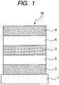
- FIG. 1 is a schematic cross-sectional view illustrating a constitution of an organic light-transmitting device according to an embodiment of the present invention.
- the benzoindenochrysene compound of the present invention is represented by the following general formula (1).
- X 1 , X 2 , X 3 , X 4 , X 5 , X 6 , X 7 , X 8 , X 9 , X 10 , X 11 , X 12 , X 13 , X 14 , X 15 , and X 16 each represent, independently of one another, a hydrogen atom, a halogen atom, a cyano group, a nitro group, a substituted or unsubstituted alkyl group, a substituted or unsubstituted alkoxy group, a substituted or unsubstituted alkenyl group, a substituted or unsubstituted alkynyl group, a substituted or unsubstituted aralkyl group, a substituted amino group, a substituted or unsubstituted aryl group, a substituted or unsubstituted heterocyclic group, or a substituted or unsubstituted
- halogen atom that is represented by X 1 to X 16
- a fluorine, a chlorine, a bromine, an iodine and the like can be mentioned.
- the present invention is not limited thereto.
- an alkyl group that is represented by X 1 to X 16
- a methyl group, an ethyl group, an n-propyl group, an iso-propyl group, an n-butyl group, an iso-butyl group, a sec-butyl group, a tert-butyl group, an n-pentyl group, a neopentyl group, an n-hexyl group, an n-octyl group, an n-decyl group, an n-dodecyl group, a cyclopropyl group, a cyclobutyl group, a cyclopentyl group, a cyclohexyl group, a norbornyl group, an adamantyl group and the like can be mentioned.
- the present invention is not limited thereto.
- an alkoxy group that is represented by X 1 to X 16
- a methoxy group, an ethoxy group, a propoxy group and the like can be mentioned.
- the present invention is not limited thereto.
- alkenyl group that is represented by X 1 to X 16
- a vinyl group a propenyl group, a butenyl group, a phenylvinyl group, a diphenylvinyl group and the like
- the present invention is not limited thereto.
- an alkynyl group that is represented by X 1 to X 16
- an ethynyl group, a propynyl group, a butynyl group, a phenethynyl group and the like can be mentioned.
- the present invention is not limited thereto.
- aralkyl group that is represented by X 1 to X 16
- a benzyl group, a phenethyl group and the like can be mentioned.
- the present invention is not limited thereto.
- a substituted amino group that is represented by X 1 to X 16
- a dimethylamino group, a diethylamino group, a dibenzylamino group, a diphenylamino group, a ditrylamino group, a ditertiary butylamino group, a dianisolyl amino group, a carbazolyl group and the like can be mentioned.
- the present invention is not limited thereto.
- an aryl group that is represented by X 1 to X 16
- a phenyl group, a naphthyl group, an azulenyl group, an acenaphthylenyl group, an indacenyl group, a biphenyl group, a fluorenyl group, an anthryl group, a phenanthryl group, a pyrenyl group, a chrysenyl group, a benzofluorenyl group, a tetraphenyl group, a naphthacenyl group, a triphenylenyl group, a fluoranthenyl group, a pycenyl group, a pentacenyl group, a perylenyl group, a benzofluoranthenyl group, a naphthofluoranthenyl group, a benzo indeno chrysenyl group and the like can be
- a heterocyclic group that is represented by X 1 to X 16
- a thienyl group a pyrrolyl group, a pyridyl group, a bipyridyl group, an oxazolyl group, an oxadiazolyl group, a thiazolyl group, a thiadiazolyl group, a terthienyl group, a carbazolyl group, an acridinyl group, a phenanthrolyl group and the like
- the present invention is not limited thereto.
- aryloxy group that is represented by X 1 to X 16
- a phenoxy group and the like can be mentioned.
- the present invention is not limited thereto.
- alkyl group such as a methyl group, an ethyl group, a propyl group, an iso-propyl group, and a tert-butyl group
- an aryl group such as a phenyl group, a naphthyl group, and a biphenyl
- a heterocyclic group such as a thienyl group, a pyrrolyl group, and a pyridyl group
- substituted amino group such as a dimethylamino group, a diethylamino group, a dibenzylamino group, a diphenylamino group, a ditrylamino group, and a dianisolyl amino
- an alkoxy group such as a methyl group, an ethyl group, a propyl group, an iso-propyl group, and a tert-butyl group
- an aryl group such as a phenyl group, a nap
- the benzoindenochrysene compound that is represented by the Formula (1) is preferably a compound represented by the following Formula (2).
- X 17 , X 18 , X 19 , X 20 , and X 21 each represent, independently of one another, a hydrogen atom or a substituted or unsubstituted aryl group.
- an aryl group that is represented by X 17 to X 21
- a phenyl group, a naphthyl group, an azulenyl group, an acenaphthylenyl group, an indacenyl group, a biphenyl group, a fluorenyl group, an anthryl group, a phenanthryl group, a pyrenyl group, a chrysenyl group, a benzofluorenyl group, a tetraphenyl group, a naphthacenyl group, a triphenylenyl group, a fluoranthenyl group, a pycenyl group, a pentacenyl group, a perylenyl group, a benzofluoranthenyl group, a naphthofluoranthenyl group, a benzo indeno chrysenyl group and the like can be
- aryl group may further have, there are included an alkyl group such as a methyl group, an ethyl group, a propyl group, an iso-propyl group, and a tert-butyl group and an aryl group such as a phenyl group, a naphthyl group, and a biphenyl group can be mentioned.
- alkyl group such as a methyl group, an ethyl group, a propyl group, an iso-propyl group, and a tert-butyl group
- an aryl group such as a phenyl group, a naphthyl group, and a biphenyl group can be mentioned.
- the present invention is not limited thereto.
- the emission efficiency As one way of extending the lifetime of an organic light-emitting device, improving the emission efficiency can be mentioned.
- the emission efficiency is improved, since the voltage that is applied to the device for obtaining light emission with a specific luminance can be decreased, not only power consumption can be reduced, but also degradation of the device due to carrier conduction can be reduced. Consequently, the lifetime of the organic light-emitting device can be extended.
- the present inventors measured emission quantum yield in dilute solution of the benzoindenochrysene compound of the present invention and naphthofluoranthene of the prior art (dilute toluene solution with a concentration of 10 -6 mol/l). As a result, data shown in Table 1 was obtained. Incidentally, the quantum yields in Table 1 are relative quantum yield when the quantum yield of naphthofluoranthene of the prior art is set to 1. (Table 1) Compound Structural formula Relative quantum yield Naphthofluoranthene 1.00 B-1 2.22 E-25 2.32 B-7 2.32 E-28 2.41
- the emission quantum yield of the benzoindenochrysene compound of the present invention is higher than that of naphthofluoranthene of the prior art. Therefore, by using the benzoindenochrysene of the present invention as a guest for a light-emitting layer, for example, the emission efficiency of an organic light-emitting device can be improved.
- emission maximum wavelengths for the benzoindenochrysene compounds of the present invention are shown in Table 2.
- Table 2 Compound Structural formula Emission maximum wavelength Naphthofluoranthene 420 nm Benzo[k] fluoranthene 410 nm B-1 430 nm E-30 443 nm E-34 445 nm
- the benzoindenochrysene compounds shown in Table 2 are representative examples. With respect to the benzoindenochrysene compound of the present invention, the emission maximum wavelength is 430 nm even for those having a short wavelength. By further introducing a substituent group, shift to a longer wavelength can be achieved. Since the emission maximum wavelength which is suitable for a blue light-emitting material is within the range of 440 nm to 480 nm, in terms of the use as a blue light-emitting material, it is sufficient to increase the emission maximum wavelength by about 10 nm or less. In this case, the increase of the emission maximum wavelength by about 10 nm can be achieved by introduction of a substituent group having a relatively small size, for example, an aryl group including a naphthyl group and the like.
- the emission maximum wavelengths of benzofluoranthene and naphthofluoranthene which are analogous compounds, are 410 nm and 420 nm, respectively, if it is desired to use them as blue light-emitting materials, the emission maximum wavelength needs to be increased by about 30 nm at the maximum. In this case, in order to increase the emission maximum wavelength by about 30 nm or so, since a substituent group having relatively narrow energy gap needs to be introduced, the types of the substituent groups which can be introduced are limited.
- the benzoindenochrysene compound of the present invention preferably consists of hydrocarbon only. This is because, when the compound itself consists of hydrocarbon only, purification is easier as compared to a compound containing a heteroatom.
- the reason for easier purification includes that, in general a molecule containing a heterocycle or a heteroatom is highly polar because of having a lone pair of electrons and may easily incorporate ionic impurities as compared to a molecule consisting of hydrocarbon only. It has been known that when an impurity is incorporated into a material which constitutes an organic light-emitting device, the performance of the device is significantly impaired due to the presence of such an impurity.
- the compound concerned consists only of hydrocarbon which hardly incorporates any impurity. Furthermore, since the electron-donating property or electron-withdrawing property of a heterocyclic group or a heteroatom is stronger than that of hydrocarbon, the energy value or energy gap of HOMO-LUMO of the molecule is significantly large or small. Meanwhile, the energy level (HOMO, LUMO) of a compound consisting of hydrocarbon only can be varied symmetrically depending on the conjugation length of the molecule, and therefore it is also advantageous in that a compound having desired energy level and energy gap can be easily designed.
- the compound E-25 in which a naphthyl group is introduced to X 21 position of the compound B-1 of the Formula (2), has a wavelength that is increased by about 5 nm as compared to the compound B-1.
- a phenyl group which has narrower energy gap as compared to a naphthyl group
- the wavelength is increased by 8 nm.
- the emission maximum wavelength can be increased more largely as compared to a case in which the introduction is made to X 21 position.
- it is preferable that a substituent group is introduced into any one of X 18 and X 19 of the Formula (2).
- a substituent group when X 27 is a hydrogen atom, a substituent group can be further introduced into X 27 position by following the method shown in Scheme 4. Specifically, by appropriately selecting a boronic acid derivative, it is possible to introduce a substituent group that is represented by X 38 to X 21 of the Formula (2). In this case, since the halogenation reaction shown in Scheme 4 has regioselectivity, a difficult purification process such as removal of positional substituent group is not required. In addition, by reacting the benzoindenochrysene compound in which a halogen atom has been introduced by the halogenation reaction with various boronic acid derivatives using Suzuki coupling reaction, various compounds can be easily synthesized. Furthermore, when a substituent group is introduced into X 21 of the Formula (2), desired physical properties such as improved emission efficiency and inhibited concentration quenching can be obtained depending on the type of the substituent group.
- the organic light-emitting device of the present invention includes an anode and a cathode, and an organic compound layer that is disposed between the anode and the cathode.
- the organic compound layer that is provided between the anode and the cathode of the organic light-emitting device may be either a single layer or a plurality of layers.
- a first layer constitution is a constitution in which a substrate, an anode, a light-emitting layer and a cathode are stacked in the mentioned order.
- a second layer constitution is a constitution in which a substrate, an anode, a hole transport layer, an electron transport layer, and a cathode are stacked in the mentioned order.
- a third layer constitution is a constitution in which a substrate, an anode, a hole transport layer, a light-emitting layer, an electron transport layer and a cathode are stacked in the mentioned order.
- FIG. 1 illustrates an organic light-emitting device 30.
- reference numeral 1 denotes a substrate such as a glass plate
- 2 denotes an anode
- 5 denotes a hole transport layer
- 3 denotes a light-emitting layer
- 6 denotes an electron transport layer
- 4 denotes a cathode.
- the anode 2 is, for example, a reflection side electrode and is formed of a reflective member or a transparent electrode having a reflective member.
- the cathode 4 is, for example, a light extracting electrode.
- the cathode is a light-transmissive electrode such as ITO.
- the benzoindenochrysene compound of the present invention can be contained in any one of the layers that are provided in the layer constitutions described above.
- an organic light-emitting device which uses the benzoindenochrysene compound of the present invention is not limited to those described above.
- other various layer constitutions are available and a constitution in which an insulating layer, an adhesive layer or an interfering layer is provided at an interface between an electrode and an organic compound layer, a constitution in which a hole transport layer consists of two layers having different ionization potentials, a constitution in which an light-emitting layer has a stacked structure with at least two layers, etc. can be mentioned.
- the benzoindenochrysene compound of the present invention which is contained in one layer may be a single species or a plurality of species.
- the benzoindenochrysene compound of the present invention is preferably contained in any one layer of a light-emitting layer, a hole transport layer and an electron transport layer. More preferably, it is contained in a light-emitting layer.
- the light-emitting layer consists of only the benzoindenochrysene compound of the present invention.
- the light-emitting layer consists of a host and a guest.
- the guest is a compound which is responsible for major light emission in a light-emitting layer.
- the host is a compound which is present as a matrix around a guest in a light-emitting layer, and it is mainly responsible for carrier transport and supply of excitation energy to a guest.
- the benzoindenochrysene compound of the present invention is preferably used as a guest.
- the emission efficiency of the organic light-emitting device is improved and light emission with high luminance can be maintained for a long period of time.
- benzoindenochrysene compound of the present invention is not limited to a material for constituting a light-emitting layer.
- it can be used as a constitutional material for a hole transport layer, an electron transport layer, a hole blocking layer, an electron blocking layer, a hole injection layer, an electron injection layer and the like.
- the organic light-emitting device of the present invention uses the benzoindenochrysene compound of the present invention as a constitution material of a light-emitting layer, in particular.
- a low molecular weight type and a polymer type hole transport compound, light-emitting compound, electron transport compound and the like that are hitherto known in the field can be also used together.
- a hole injection transport material a material which is suitable for easy hole injection from an anode and has a high hole transporting property to transport the injected hole to a light-emitting layer is preferable.
- a low molecular weight type and a polymer type material having a hole injection transporting property include, but not limited to, a triarylamine derivative, a phenylene diamine derivative, a stilbene derivative, a phthalocyanin derivative, a porphyrin derivative, poly(vinylcarbazole), poly(thiophene) and other conductive polymers.
- a fused ring compound for example, a fluorene derivative, a pyrene derivative, a tetracene derivative, 9,10-diphenylanthracene derivative, lubrene and the like
- a quinacridone derivative for example, a quinacridone derivative, a coumarine derivative, a stilbene derivative, an organoaluminum complex such as tris(8-quinolinolate)aluminum, an organoberyllium complex
- a polymer derivative such as a poly(phenylenevinylene) derivative, a poly(fluorene) derivative, and a poly(phenylene) derivative can be mentioned, but not limited thereto.
- an electron injection transport material any one that is suitable for easy electron injection from a cathode and can transport the injected electron to a light-emitting layer can be selected, and it is selected in consideration of balance with carrier transporting property of a hole transport material, etc.
- a material having an electron injection transporting property include, but not limited to, an oxadiazole derivative, an oxazole derivative, a pyrazine derivative, a triazole derivative, a triazine derivative, a quinoline derivative, a quinoxaline derivative, a phenanthroline derivative, an organoaluminum complex and the like.
- a material constituting an anode those having as large a work function as possible are preferred.
- a metal element such as gold, platinum, silver, copper, nickel, palladium, cobalt, selenium, vanadium, and tungsten, or alloys of these elements, or a metal oxide such as tin oxide, zinc oxide, indium oxide, indium tin oxide (ITO), and zinc indium oxide.
- a conductive polymer such as polyaniline, polypyrrole, and polythiophene can be also used. These electrode materials can be used alone or in combination of two or more.
- the anode may consist of one layer or a plurality of layers.
- a material constituting a cathode those having as small a work function as possible are preferred.
- examples thereof include an alkali metal such as lithium, an alkali earth metal such as calcium, and an elemental metal such as aluminum, titanium, manganese, silver, lead, and chromium.
- An alloy combining these metal elements can be also used.
- magnesium-silver, aluminum-lithium, aluminum-magnesium and the like can be used.
- a metal oxide such as indium tin oxide (ITO) can be also used.
- ITO indium tin oxide
- the cathode may consist of one layer or a plurality of layers.
- the substrate used in the organic light-emitting device of the present invention is not particularly limited, but an opaque substrate such as a metal substrate, and a ceramic substrate or a transparent substrate such as glass, quartz, and a plastic sheet can be used.
- a color filter film, a fluorescent color conversion filter film, a dielectric reflection film and the like can be used for the substrate to control the emitted light.
- the produced device may be provided with a protective layer or an encapsulating layer for the purpose of preventing the device from contacting oxygen or moisture, and the like, for example.
- the protective layer include a diamond thin film, an inorganic material film made of, for example, a metal oxide or a metal nitride, a polymer film such as fluororesin, polyethylene, silicone resin, or polystyrene resin, and a photocurable resin and the like.
- the device may be covered with glass, a gas impermeable film, a metal, or the like, and the device itself can be packaged with an appropriate encapsulating resin.
- TFT thin film transistor
- both a bottom emission configuration i.e., a configuration in which light is extracted from a substrate side
- a top emission configuration i.e., a configuration in which light is extracted from the side opposite to the substrate side
- an organic compound layer including a layer which contains the benzoindenochrysene compound of the present invention is formed by the processes described below.
- a thin film is formed by a vacuum evaporation process, an ionized evaporation process, a sputtering process, or a plasma process, or by dissolving a film material in an appropriate solvent and subjecting the solution to a known application method (such as a spin coating process, a dipping process, a casting process, an LB process, or an ink jet process).
- a film when a layer is formed by a vacuum evaporation process or by a solution coating process, crystallization and the like hardly occurs and the stability over time is excellent. Furthermore, when a film is formed by the coating method, a film may be formed by additionally using an appropriate binder resin.
- binder resin examples include, but are not limited to, a polyvinyl carbazole resin, a polycarbonate resin, a polyester resin, an ABS resin, an acrylic resin, a polyimide resin, a phenol resin, an epoxy resin, a silicone resin, a urea resin and the like. Furthermore, these binder resins are used in the form of a homopolymer or a copolymer. Moreover, they can be used alone or in combination of two or more. Still furthermore, if required, a known additive such as a plasticizer, an antioxidant, and a UV absorber may be used in combination with the binder resin.
- the reaction solution was cooled to -78°C and 55.6 g (438 mmol) of oxalyl chloride was added dropwise thereto with stirring at that temperature. Then, while maintaining the liquid temperature at -78°C, the reaction solution was stirred for 30 minutes and warmed to room temperature over 2 hours. Next, the reaction solution was poured into 4L of ice water with stirring and a resulting solid was separated by filtration. Then, the solid was dispersed and washed with 100 mL of methanol. After washing, the solid was vacuum dried with heating to give 21.5 g (yield: 87%) of Compound 2.
- reaction solution was heated to 85°C and stirred for 5 hours at that temperature. Then, after cooling the reaction solution, liquid-liquid separation was carried out with 1M aqueous hydrochloric acid solution, aqueous sodium hydrocarbonate solution, and aqueous sodium chloride solution sequentially and the organic layer was recovered. After drying the organic layer over sodium sulfate, the solvent was evaporated under reduced pressure to give a crude product.
- reaction solution was heated to 85°C and stirred for 4 hours at that temperature.
- liquid-liquid separation was carried out with 1M aqueous hydrochloric acid solution, aqueous sodium hydrogen carbonate solution, and aqueous sodium chloride solution sequentially and the organic layer was recovered.
- the solvent was evaporated under reduced pressure to give a crude product.
- the crude product was purified with column chromatography (chromatography gel: BW300 (trade name; manufactured by FUJI SILYSIA CHEMICAL LTD.); developing solvent: toluene), and recrystallized from toluene to give 3.1 g (5.3 mmol) of Compound 6 (yield: 60.2%).
- An organic light-emitting device having a layer constitution as described in the third layer constitution above and shown in FIG. 1 was produced according to the following method.
- an indium tin oxide (ITO) film By forming an indium tin oxide (ITO) film on a glass substrate using a sputtering method, an anode was formed. The film thickness of the anode 2 was 120 nm. Next, the substrate on which the ITO electrode has been formed was ultrasonically cleaned sequentially with acetone and isopropyl alcohol (IPA), and then washed with boiled IPA. After drying, the substrate was cleaned with UV/ozone. The substrate treated according to the method described above was used as a transparent conductive support substrate.
- ITO indium tin oxide
- the substrate having the layers up to and including the hole transport layer formed thereon was transferred to a vacuum chamber.
- a vacuum chamber After adjusting the inside pressure of the vacuum chamber to 10 -5 Pa, with vacuum evaporation based on resistive heating, continuous film formation of an organic compound layer and an electrode layer on the hole transport layer was carried out.
- Compound 8 as a host shown below and Exemplified Compound E-28 as a guest were co-evaporated in a weight concentration ratio of 95 to 5 to form a light-emitting layer. At this time, the film thickness of the light-emitting layer was 20 nm.
- film formation of Compound 8 shown below was carried out to form an electron transport layer. At this time, the film thickness of the electron transport layer was 40 nm.
- LiF film formation was carried out to form a first metal electrode layer. At this time, the film thickness of the first metal electrode layer was 0.5 nm.
- Al film formation was carried out to form a second metal electrode layer. At this time, the film thickness of the second metal electrode layer was 150 nm. As a result, an organic light-emitting device was obtained.
- Pico-Amp Meter 4140B manufactured by Hewlett-Packard Development Company L.P.
- BM7 manufactured by TOPCON CORP
- Organic light-emitting devices were prepared by following the same procedure as in Example 5 with the exception that the host and the guest and their mixing ratio by weight in the light-emitting layer were changed to those shown in Table 4 below. With the resulting devices, the evaluation was carried out in the same manner as in Example 5. The results are shown in Table 4.
Landscapes
- Chemical & Material Sciences (AREA)
- Organic Chemistry (AREA)
- Engineering & Computer Science (AREA)
- Materials Engineering (AREA)
- Physics & Mathematics (AREA)
- Spectroscopy & Molecular Physics (AREA)
- Optics & Photonics (AREA)
- Electroluminescent Light Sources (AREA)
- Organic Low-Molecular-Weight Compounds And Preparation Thereof (AREA)
Applications Claiming Priority (2)
| Application Number | Priority Date | Filing Date | Title |
|---|---|---|---|
| JP2008314391A JP5414258B2 (ja) | 2008-12-10 | 2008-12-10 | ベンゾインデノクリセン化合物及びこれを用いた有機発光素子 |
| PCT/JP2009/070359 WO2010067757A1 (en) | 2008-12-10 | 2009-11-27 | Benzoindenochrysene compound and organic light-emitting device using the same |
Publications (3)
| Publication Number | Publication Date |
|---|---|
| EP2376407A1 EP2376407A1 (en) | 2011-10-19 |
| EP2376407A4 EP2376407A4 (en) | 2012-11-14 |
| EP2376407B1 true EP2376407B1 (en) | 2017-07-05 |
Family
ID=42242745
Family Applications (1)
| Application Number | Title | Priority Date | Filing Date |
|---|---|---|---|
| EP09831861.1A Not-in-force EP2376407B1 (en) | 2008-12-10 | 2009-11-27 | Radio-opaque bioactiveglass materials |
Country Status (7)
| Country | Link |
|---|---|
| US (1) | US20110240982A1 (enExample) |
| EP (1) | EP2376407B1 (enExample) |
| JP (1) | JP5414258B2 (enExample) |
| KR (1) | KR101392567B1 (enExample) |
| CN (1) | CN102245544A (enExample) |
| RU (1) | RU2469015C1 (enExample) |
| WO (1) | WO2010067757A1 (enExample) |
Families Citing this family (5)
| Publication number | Priority date | Publication date | Assignee | Title |
|---|---|---|---|---|
| JP4637253B2 (ja) * | 2009-06-30 | 2011-02-23 | キヤノン株式会社 | 新規有機化合物および有機発光素子および画像表示装置 |
| JP5606861B2 (ja) * | 2010-09-30 | 2014-10-15 | ユー・ディー・シー アイルランド リミテッド | 有機電界発光素子用材料、膜、発光層、有機電界発光素子、及び有機電界発光素子の製造方法 |
| JP6189090B2 (ja) * | 2012-06-01 | 2017-08-30 | 株式会社半導体エネルギー研究所 | 有機材料の製造方法、発光素子の製造方法、発光装置の製造方法及び照明装置の製造方法 |
| JP6016511B2 (ja) * | 2012-08-07 | 2016-10-26 | キヤノン株式会社 | 新規縮合多環化合物、それを有する有機発光素子、表示装置、画像情報処理装置、照明装置及び画像形成装置 |
| JP5774076B2 (ja) * | 2013-11-14 | 2015-09-02 | キヤノン株式会社 | ベンゾインデノクリセン化合物及びこれを用いた有機発光素子 |
Family Cites Families (9)
| Publication number | Priority date | Publication date | Assignee | Title |
|---|---|---|---|---|
| RU2123773C1 (ru) * | 1998-04-20 | 1998-12-20 | Некоммерческое партнерство "Полимерная электроника" | Электролюминесцентное устройство и способ его изготовления |
| JP4562884B2 (ja) * | 2000-08-25 | 2010-10-13 | 出光興産株式会社 | 有機エレクトロルミネッセンス素子 |
| ITTO20020033A1 (it) * | 2002-01-11 | 2003-07-11 | Fiat Ricerche | Dispositivo elettro-luminescente. |
| TWI314947B (en) * | 2002-04-24 | 2009-09-21 | Eastman Kodak Compan | Organic light emitting diode devices with improved operational stability |
| EP2085371B1 (en) * | 2006-11-15 | 2015-10-07 | Idemitsu Kosan Co., Ltd. | Fluoranthene compound, organic electroluminescent device using the fluoranthene compound, and organic electroluminescent material-containing solution |
| JP5142589B2 (ja) * | 2007-05-28 | 2013-02-13 | キヤノン株式会社 | インデノクリセン誘導体及びそれを用いた有機発光素子 |
| JP2009009966A (ja) * | 2007-06-26 | 2009-01-15 | Mitsui Chemicals Inc | 有機トランジスタ |
| JP5335284B2 (ja) * | 2008-05-22 | 2013-11-06 | キヤノン株式会社 | 縮合多環化合物およびそれを有する有機発光素子 |
| JPWO2010018842A1 (ja) * | 2008-08-12 | 2012-01-26 | 出光興産株式会社 | ベンゾフルオランテン誘導体及びそれを用いた有機エレクトロルミネッセンス素子 |
-
2008
- 2008-12-10 JP JP2008314391A patent/JP5414258B2/ja not_active Expired - Fee Related
-
2009
- 2009-11-27 EP EP09831861.1A patent/EP2376407B1/en not_active Not-in-force
- 2009-11-27 KR KR1020117015300A patent/KR101392567B1/ko active Active
- 2009-11-27 US US13/133,631 patent/US20110240982A1/en not_active Abandoned
- 2009-11-27 CN CN2009801492655A patent/CN102245544A/zh active Pending
- 2009-11-27 RU RU2011128406/04A patent/RU2469015C1/ru not_active IP Right Cessation
- 2009-11-27 WO PCT/JP2009/070359 patent/WO2010067757A1/en not_active Ceased
Non-Patent Citations (1)
| Title |
|---|
| None * |
Also Published As
| Publication number | Publication date |
|---|---|
| US20110240982A1 (en) | 2011-10-06 |
| RU2469015C1 (ru) | 2012-12-10 |
| CN102245544A (zh) | 2011-11-16 |
| JP2010138086A (ja) | 2010-06-24 |
| EP2376407A1 (en) | 2011-10-19 |
| JP5414258B2 (ja) | 2014-02-12 |
| KR20110101181A (ko) | 2011-09-15 |
| KR101392567B1 (ko) | 2014-05-08 |
| WO2010067757A1 (en) | 2010-06-17 |
| EP2376407A4 (en) | 2012-11-14 |
Similar Documents
| Publication | Publication Date | Title |
|---|---|---|
| US20220029097A1 (en) | Aromatic amine derivative, and organic electroluminescent element comprising the same | |
| CN103328420B (zh) | 蒽化合物及使用其的有机电激发光元件、发光层用材料、显示装置及照明装置 | |
| US8932735B2 (en) | Aromatic amine derivative and organic electroluminescent element comprising the same | |
| US9051232B2 (en) | Perylene compound and organic light emitting device using the compound | |
| JP5110901B2 (ja) | 有機発光素子用材料およびそれを用いた有機発光素子 | |
| EP2700696A1 (en) | Pyrene derivative, organic light-emitting medium, and organic electroluminescent element containing pyrene derivative or organic light-emitting medium | |
| CN102629663A (zh) | 新型化合物和使用该化合物的有机发光器件 | |
| WO2012098793A1 (en) | Organic compound, organic electroluminescence element, and image display device | |
| EP2634170A1 (en) | Aromatic amine derivative, and organic electroluminescent element using same | |
| EP2376407B1 (en) | Radio-opaque bioactiveglass materials | |
| EP2291342B1 (en) | DIBENZO[c,g]FLUORENE COMPOUND AND AN ORGANIC LIGHT-EMITTING DEVICE USING THE SAME | |
| KR101490575B1 (ko) | 신규한 유기 화합물 및 이를 포함하는 유기 발광 소자 | |
| US20110272683A1 (en) | Novel bichrysene compound and organic light emitting device having the compound | |
| EP2956431A1 (en) | Novel fused polycyclic compound and organic light emitting element including the same | |
| US9178161B2 (en) | Benzo[c]phenanthrene compound and organic light-emitting device containing same | |
| US8642191B2 (en) | Fused polycyclic compound and organic light-emitting element | |
| RU2459795C1 (ru) | Органическое соединение и органическое светоизлучающее устройство, в котором применяется такое органическое соединение | |
| JP5774076B2 (ja) | ベンゾインデノクリセン化合物及びこれを用いた有機発光素子 | |
| US8771842B2 (en) | Benzo[b]chrysene compound and organic light-emitting element including the same | |
| WO2010053141A1 (en) | Dibenzo[c,g]fluorene compound and organic light-emitting device using same |
Legal Events
| Date | Code | Title | Description |
|---|---|---|---|
| PUAI | Public reference made under article 153(3) epc to a published international application that has entered the european phase |
Free format text: ORIGINAL CODE: 0009012 |
|
| 17P | Request for examination filed |
Effective date: 20110711 |
|
| AK | Designated contracting states |
Kind code of ref document: A1 Designated state(s): AT BE BG CH CY CZ DE DK EE ES FI FR GB GR HR HU IE IS IT LI LT LU LV MC MK MT NL NO PL PT RO SE SI SK SM TR |
|
| DAX | Request for extension of the european patent (deleted) | ||
| A4 | Supplementary search report drawn up and despatched |
Effective date: 20121016 |
|
| RIC1 | Information provided on ipc code assigned before grant |
Ipc: H01L 51/00 20060101ALI20121010BHEP Ipc: H05B 33/14 20060101ALI20121010BHEP Ipc: C07C 43/275 20060101ALI20121010BHEP Ipc: C07C 25/22 20060101ALI20121010BHEP Ipc: C07C 13/62 20060101AFI20121010BHEP Ipc: C09K 11/06 20060101ALI20121010BHEP Ipc: C07C 43/21 20060101ALI20121010BHEP Ipc: C07D 471/04 20060101ALI20121010BHEP Ipc: C07C 205/11 20060101ALI20121010BHEP Ipc: C07C 255/52 20060101ALI20121010BHEP Ipc: H01L 51/50 20060101ALI20121010BHEP |
|
| GRAP | Despatch of communication of intention to grant a patent |
Free format text: ORIGINAL CODE: EPIDOSNIGR1 |
|
| INTG | Intention to grant announced |
Effective date: 20130710 |
|
| 17Q | First examination report despatched |
Effective date: 20140528 |
|
| INTC | Intention to grant announced (deleted) | ||
| GRAP | Despatch of communication of intention to grant a patent |
Free format text: ORIGINAL CODE: EPIDOSNIGR1 |
|
| INTG | Intention to grant announced |
Effective date: 20170125 |
|
| GRAS | Grant fee paid |
Free format text: ORIGINAL CODE: EPIDOSNIGR3 |
|
| GRAA | (expected) grant |
Free format text: ORIGINAL CODE: 0009210 |
|
| AK | Designated contracting states |
Kind code of ref document: B1 Designated state(s): AT BE BG CH CY CZ DE DK EE ES FI FR GB GR HR HU IE IS IT LI LT LU LV MC MK MT NL NO PL PT RO SE SI SK SM TR |
|
| REG | Reference to a national code |
Ref country code: GB Ref legal event code: FG4D |
|
| REG | Reference to a national code |
Ref country code: CH Ref legal event code: EP |
|
| REG | Reference to a national code |
Ref country code: AT Ref legal event code: REF Ref document number: 906493 Country of ref document: AT Kind code of ref document: T Effective date: 20170715 |
|
| REG | Reference to a national code |
Ref country code: IE Ref legal event code: FG4D |
|
| REG | Reference to a national code |
Ref country code: DE Ref legal event code: R096 Ref document number: 602009047031 Country of ref document: DE |
|
| REG | Reference to a national code |
Ref country code: NL Ref legal event code: MP Effective date: 20170705 |
|
| REG | Reference to a national code |
Ref country code: AT Ref legal event code: MK05 Ref document number: 906493 Country of ref document: AT Kind code of ref document: T Effective date: 20170705 |
|
| REG | Reference to a national code |
Ref country code: LT Ref legal event code: MG4D |
|
| PG25 | Lapsed in a contracting state [announced via postgrant information from national office to epo] |
Ref country code: FI Free format text: LAPSE BECAUSE OF FAILURE TO SUBMIT A TRANSLATION OF THE DESCRIPTION OR TO PAY THE FEE WITHIN THE PRESCRIBED TIME-LIMIT Effective date: 20170705 Ref country code: HR Free format text: LAPSE BECAUSE OF FAILURE TO SUBMIT A TRANSLATION OF THE DESCRIPTION OR TO PAY THE FEE WITHIN THE PRESCRIBED TIME-LIMIT Effective date: 20170705 Ref country code: LT Free format text: LAPSE BECAUSE OF FAILURE TO SUBMIT A TRANSLATION OF THE DESCRIPTION OR TO PAY THE FEE WITHIN THE PRESCRIBED TIME-LIMIT Effective date: 20170705 Ref country code: NO Free format text: LAPSE BECAUSE OF FAILURE TO SUBMIT A TRANSLATION OF THE DESCRIPTION OR TO PAY THE FEE WITHIN THE PRESCRIBED TIME-LIMIT Effective date: 20171005 Ref country code: NL Free format text: LAPSE BECAUSE OF FAILURE TO SUBMIT A TRANSLATION OF THE DESCRIPTION OR TO PAY THE FEE WITHIN THE PRESCRIBED TIME-LIMIT Effective date: 20170705 Ref country code: AT Free format text: LAPSE BECAUSE OF FAILURE TO SUBMIT A TRANSLATION OF THE DESCRIPTION OR TO PAY THE FEE WITHIN THE PRESCRIBED TIME-LIMIT Effective date: 20170705 Ref country code: SE Free format text: LAPSE BECAUSE OF FAILURE TO SUBMIT A TRANSLATION OF THE DESCRIPTION OR TO PAY THE FEE WITHIN THE PRESCRIBED TIME-LIMIT Effective date: 20170705 |
|
| PG25 | Lapsed in a contracting state [announced via postgrant information from national office to epo] |
Ref country code: PL Free format text: LAPSE BECAUSE OF FAILURE TO SUBMIT A TRANSLATION OF THE DESCRIPTION OR TO PAY THE FEE WITHIN THE PRESCRIBED TIME-LIMIT Effective date: 20170705 Ref country code: GR Free format text: LAPSE BECAUSE OF FAILURE TO SUBMIT A TRANSLATION OF THE DESCRIPTION OR TO PAY THE FEE WITHIN THE PRESCRIBED TIME-LIMIT Effective date: 20171006 Ref country code: LV Free format text: LAPSE BECAUSE OF FAILURE TO SUBMIT A TRANSLATION OF THE DESCRIPTION OR TO PAY THE FEE WITHIN THE PRESCRIBED TIME-LIMIT Effective date: 20170705 Ref country code: BG Free format text: LAPSE BECAUSE OF FAILURE TO SUBMIT A TRANSLATION OF THE DESCRIPTION OR TO PAY THE FEE WITHIN THE PRESCRIBED TIME-LIMIT Effective date: 20171005 Ref country code: IS Free format text: LAPSE BECAUSE OF FAILURE TO SUBMIT A TRANSLATION OF THE DESCRIPTION OR TO PAY THE FEE WITHIN THE PRESCRIBED TIME-LIMIT Effective date: 20171105 Ref country code: ES Free format text: LAPSE BECAUSE OF FAILURE TO SUBMIT A TRANSLATION OF THE DESCRIPTION OR TO PAY THE FEE WITHIN THE PRESCRIBED TIME-LIMIT Effective date: 20170705 |
|
| REG | Reference to a national code |
Ref country code: DE Ref legal event code: R097 Ref document number: 602009047031 Country of ref document: DE |
|
| PG25 | Lapsed in a contracting state [announced via postgrant information from national office to epo] |
Ref country code: CZ Free format text: LAPSE BECAUSE OF FAILURE TO SUBMIT A TRANSLATION OF THE DESCRIPTION OR TO PAY THE FEE WITHIN THE PRESCRIBED TIME-LIMIT Effective date: 20170705 Ref country code: DK Free format text: LAPSE BECAUSE OF FAILURE TO SUBMIT A TRANSLATION OF THE DESCRIPTION OR TO PAY THE FEE WITHIN THE PRESCRIBED TIME-LIMIT Effective date: 20170705 Ref country code: RO Free format text: LAPSE BECAUSE OF FAILURE TO SUBMIT A TRANSLATION OF THE DESCRIPTION OR TO PAY THE FEE WITHIN THE PRESCRIBED TIME-LIMIT Effective date: 20170705 |
|
| PLBE | No opposition filed within time limit |
Free format text: ORIGINAL CODE: 0009261 |
|
| STAA | Information on the status of an ep patent application or granted ep patent |
Free format text: STATUS: NO OPPOSITION FILED WITHIN TIME LIMIT |
|
| PG25 | Lapsed in a contracting state [announced via postgrant information from national office to epo] |
Ref country code: IT Free format text: LAPSE BECAUSE OF FAILURE TO SUBMIT A TRANSLATION OF THE DESCRIPTION OR TO PAY THE FEE WITHIN THE PRESCRIBED TIME-LIMIT Effective date: 20170705 Ref country code: SM Free format text: LAPSE BECAUSE OF FAILURE TO SUBMIT A TRANSLATION OF THE DESCRIPTION OR TO PAY THE FEE WITHIN THE PRESCRIBED TIME-LIMIT Effective date: 20170705 Ref country code: SK Free format text: LAPSE BECAUSE OF FAILURE TO SUBMIT A TRANSLATION OF THE DESCRIPTION OR TO PAY THE FEE WITHIN THE PRESCRIBED TIME-LIMIT Effective date: 20170705 Ref country code: EE Free format text: LAPSE BECAUSE OF FAILURE TO SUBMIT A TRANSLATION OF THE DESCRIPTION OR TO PAY THE FEE WITHIN THE PRESCRIBED TIME-LIMIT Effective date: 20170705 |
|
| 26N | No opposition filed |
Effective date: 20180406 |
|
| PG25 | Lapsed in a contracting state [announced via postgrant information from national office to epo] |
Ref country code: MC Free format text: LAPSE BECAUSE OF FAILURE TO SUBMIT A TRANSLATION OF THE DESCRIPTION OR TO PAY THE FEE WITHIN THE PRESCRIBED TIME-LIMIT Effective date: 20170705 |
|
| GBPC | Gb: european patent ceased through non-payment of renewal fee |
Effective date: 20171127 |
|
| PG25 | Lapsed in a contracting state [announced via postgrant information from national office to epo] |
Ref country code: CH Free format text: LAPSE BECAUSE OF NON-PAYMENT OF DUE FEES Effective date: 20171130 Ref country code: LI Free format text: LAPSE BECAUSE OF NON-PAYMENT OF DUE FEES Effective date: 20171130 |
|
| PG25 | Lapsed in a contracting state [announced via postgrant information from national office to epo] |
Ref country code: LU Free format text: LAPSE BECAUSE OF NON-PAYMENT OF DUE FEES Effective date: 20171127 Ref country code: SI Free format text: LAPSE BECAUSE OF FAILURE TO SUBMIT A TRANSLATION OF THE DESCRIPTION OR TO PAY THE FEE WITHIN THE PRESCRIBED TIME-LIMIT Effective date: 20170705 |
|
| REG | Reference to a national code |
Ref country code: FR Ref legal event code: ST Effective date: 20180731 Ref country code: BE Ref legal event code: MM Effective date: 20171130 |
|
| REG | Reference to a national code |
Ref country code: IE Ref legal event code: MM4A |
|
| PG25 | Lapsed in a contracting state [announced via postgrant information from national office to epo] |
Ref country code: MT Free format text: LAPSE BECAUSE OF NON-PAYMENT OF DUE FEES Effective date: 20171127 |
|
| PG25 | Lapsed in a contracting state [announced via postgrant information from national office to epo] |
Ref country code: FR Free format text: LAPSE BECAUSE OF NON-PAYMENT OF DUE FEES Effective date: 20171130 Ref country code: IE Free format text: LAPSE BECAUSE OF NON-PAYMENT OF DUE FEES Effective date: 20171127 |
|
| PG25 | Lapsed in a contracting state [announced via postgrant information from national office to epo] |
Ref country code: GB Free format text: LAPSE BECAUSE OF NON-PAYMENT OF DUE FEES Effective date: 20171127 Ref country code: BE Free format text: LAPSE BECAUSE OF NON-PAYMENT OF DUE FEES Effective date: 20171130 |
|
| PG25 | Lapsed in a contracting state [announced via postgrant information from national office to epo] |
Ref country code: HU Free format text: LAPSE BECAUSE OF FAILURE TO SUBMIT A TRANSLATION OF THE DESCRIPTION OR TO PAY THE FEE WITHIN THE PRESCRIBED TIME-LIMIT; INVALID AB INITIO Effective date: 20091127 |
|
| PG25 | Lapsed in a contracting state [announced via postgrant information from national office to epo] |
Ref country code: CY Free format text: LAPSE BECAUSE OF NON-PAYMENT OF DUE FEES Effective date: 20170705 |
|
| PG25 | Lapsed in a contracting state [announced via postgrant information from national office to epo] |
Ref country code: MK Free format text: LAPSE BECAUSE OF FAILURE TO SUBMIT A TRANSLATION OF THE DESCRIPTION OR TO PAY THE FEE WITHIN THE PRESCRIBED TIME-LIMIT Effective date: 20170705 |
|
| PG25 | Lapsed in a contracting state [announced via postgrant information from national office to epo] |
Ref country code: TR Free format text: LAPSE BECAUSE OF FAILURE TO SUBMIT A TRANSLATION OF THE DESCRIPTION OR TO PAY THE FEE WITHIN THE PRESCRIBED TIME-LIMIT Effective date: 20170705 |
|
| PG25 | Lapsed in a contracting state [announced via postgrant information from national office to epo] |
Ref country code: PT Free format text: LAPSE BECAUSE OF FAILURE TO SUBMIT A TRANSLATION OF THE DESCRIPTION OR TO PAY THE FEE WITHIN THE PRESCRIBED TIME-LIMIT Effective date: 20170705 |
|
| PGFP | Annual fee paid to national office [announced via postgrant information from national office to epo] |
Ref country code: DE Payment date: 20231019 Year of fee payment: 15 |
|
| REG | Reference to a national code |
Ref country code: DE Ref legal event code: R119 Ref document number: 602009047031 Country of ref document: DE |
|
| PG25 | Lapsed in a contracting state [announced via postgrant information from national office to epo] |
Ref country code: DE Free format text: LAPSE BECAUSE OF NON-PAYMENT OF DUE FEES Effective date: 20250603 |