EP2365488A1 - Apparatus and method for testing semiconductor integrated circuits, and a non-transitory computer-readable medium having a semiconductor integrated circuit testing program - Google Patents
Apparatus and method for testing semiconductor integrated circuits, and a non-transitory computer-readable medium having a semiconductor integrated circuit testing program Download PDFInfo
- Publication number
- EP2365488A1 EP2365488A1 EP11153138A EP11153138A EP2365488A1 EP 2365488 A1 EP2365488 A1 EP 2365488A1 EP 11153138 A EP11153138 A EP 11153138A EP 11153138 A EP11153138 A EP 11153138A EP 2365488 A1 EP2365488 A1 EP 2365488A1
- Authority
- EP
- European Patent Office
- Prior art keywords
- operation condition
- information
- semiconductor integrated
- target
- test
- Prior art date
- Legal status (The legal status is an assumption and is not a legal conclusion. Google has not performed a legal analysis and makes no representation as to the accuracy of the status listed.)
- Granted
Links
Images



Classifications
-
- G—PHYSICS
- G11—INFORMATION STORAGE
- G11C—STATIC STORES
- G11C29/00—Checking stores for correct operation ; Subsequent repair; Testing stores during standby or offline operation
- G11C29/56—External testing equipment for static stores, e.g. automatic test equipment [ATE]; Interfaces therefor
-
- G—PHYSICS
- G11—INFORMATION STORAGE
- G11C—STATIC STORES
- G11C17/00—Read-only memories programmable only once; Semi-permanent stores, e.g. manually-replaceable information cards
- G11C17/14—Read-only memories programmable only once; Semi-permanent stores, e.g. manually-replaceable information cards in which contents are determined by selectively establishing, breaking or modifying connecting links by permanently altering the state of coupling elements, e.g. PROM
- G11C17/18—Auxiliary circuits, e.g. for writing into memory
Definitions
- the present invention relates to the testing of semiconductor integrated circuits.
- the invention may provide a method of testing a semiconductor integrated circuit by causing a computer to perform generating test pattern data for testing a write operation in a memory of the semiconductor integrated circuit; and writing the test pattern data into a storage area of the semiconductor integrated circuit.
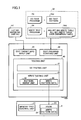
- FIG. 1 is a functional block diagram of a testing apparatus and a semiconductor chip tested by the testing apparatus
- FIG. 5 is a flowchart of an overall process performed by the testing apparatus.
- FIG. 6 illustrates a hardware structure of the testing apparatus.
- FIG. 1 is a functional block diagram of a testing apparatus 100 for testing a chip 2 (semiconductor integrated circuit).
- the testing apparatus 100 includes a test information input unit 31, a test program activating unit 32, and a testing unit 40.
- the functions of the test information input unit 31, the test program activating unit 32, and the testing unit 40 may be provided by causing a CPU (central processing unit; not shown in FIG. 1 ) to execute a control program, as will be described later.
- the test information input unit 31 is configured to receive and supply test target information 51 designating a test target to the testing unit 40.
- the test target information 51 includes a lot number, a wafer number, and a chip number, either individually or in combination.
- the lot number may be specified without designating the wafer number or the chip number; or the lot number and the wafer number may be specified without specifying the chip number. When the chip number alone is designated, the lot and the wafer may not be limited.
- the test program activating unit 32 loads test execution information 52 into a storage area of the testing apparatus 100 and then causes the testing unit 40 to initiate a test.
- the test execution information 52 includes a DC test program 53; a DC test pattern 53d used in the DC test; a write test program 54; and pattern generating data 54d.
- the testing unit 40 includes a DC testing unit 41 and a write testing unit 42.
- the DC testing unit 41 is realized upon execution of the DC test program 53 by the CPU.
- the write testing unit 42 is realized upon execution of the write test program 54 by the CPU.
- the write testing unit 42 includes a pattern merge unit 43.
- the pattern merge unit 43 generates write pattern data 44 by merging an all-bit-no-write table, an all-bit-write table, and a user definition table which are included in the pattern generating data 54d in the test execution information 52 as will be described in detail later.
- the write pattern data 44 is stored in a storage area of the testing apparatus 100.
- the all-bit-write table 5b of FIG. 2B is a default definition table of a pattern (which may be hereafter referred to as a "write pattern") for writing in all of the bits.
- the all-bit-write table 5b has items of ADD, PAD, INIT, PGM, and CYC.
- ADD designates an address count of the write pattern in decimal numbers, indicating which line is to be written.
- PAD designates terminal numbers of the PGMCMD signals.
- INIT designates values of the PGMCMD signals for a no-write operation.
- PGM indicates a value of the PGMCMD signals for a write operation.
- CYC designates the cycle time for the delivery of the no-write pattern. In the example of FIG.
- the testing unit 40 then extracts all of the combinations of the values of LOT, WAF, and CHIP from the user definition table 5c included in the pattern generating data 54d (step S72).
- the combinations of (LOT, WAF, CHIP) include (123, 10, 1), (123, 10, 2), and (234, 1, 2).
- the testing unit 40 reads the test target information 51 stored in the storage area (step S72-2).
- the testing unit 40 compares the combinations of (LOT, WAF, CHIP) extracted in step S72 with the test target information 51 read in step S72-2. If there is a combination having the corresponding item values, the routine proceeds to step S74 or step S74-2. If there is no corresponding combination, a default pattern 5d is acquired from the user definition table 5c (step S73).
- the testing unit 40 acquires from the user definition table 5c a pattern with the item values corresponding to those of the combinations (LOT, WAF, CHIP) extracted in step S72.
- the testing unit 40 identifies the ADD of the combinations from the user definition table 5c having DEF "1" indicating write targets, and then extracts the write conditions for the combinations with the identified ADD from the all-bit-write table 5b (step S74).
- the testing unit 40 then writes the all-bits pattern 8a stored in the write pattern data 44 in the PROM 23 of the chip 2 as the write pattern data 24 based on the test target information 51, thereby completing the pattern merge process (step S78).
- step S73 if it is determined in step S73 that there is no corresponding combination between the combinations (LOT, WAF, CHIP) extracted in step S72 and the test target information 51 read in step S73, steps S76 and S77 are executed.
- step S76 the testing unit 40, using only the information of DEF and ADD from the default pattern 5d in the user definition table 5c, identifies the ADD of write targets with DEF "1", and extracts the corresponding write conditions from the all-bit-write table 5b. Specifically, from the default pattern 5d of FIG.
- FIG. 5 is a flowchart of an overall process performed by the testing apparatus 100 including the above-described pattern merge process.
- the testing apparatus 100 reads the test execution information 52 into the storage area using the test program activating unit 32 (step S11).
- the test execution information 52 includes the DC test program 53, the DC test pattern 53d, the write test program 54, and the pattern generating data 54d.
- the testing apparatus 100 also reads the test target information 51 into the storage area using the test target information input unit 31 (step S12).
- the test target information 51 includes the designated lot number, wafer number, and chip number.
- the testing unit 40 Upon reception of a write test completion notice from the write testing unit 42 (step S16), the testing unit 40 determines whether the test has been completed for all of the test target chips (step S17) based on the test target information 51. If there is at least one chip that has not been tested, the testing unit 40 repeats the above process for the chip from step S13. On the other hand, if all of the test target chips have been tested, the test process is completed.
- FIG. 6 is a block diagram of a hardware structure of the testing apparatus 100.
- the testing apparatus 100 which may include a terminal controlled by a computer, includes a CPU (Central Processing Unit) 11, a memory unit 12, a display unit 13, an output unit 14, an input unit 15, an interface (I/F) 16, a storage unit 17, and a driver 18, which are connected via a system bus B.
- CPU Central Processing Unit
- memory unit 12 a memory unit 12
- display unit 13 a display unit 13
- an output unit 14 an input unit
- I/F interface
- storage unit 17 storage unit 17
- driver 18 which are connected via a system bus B.
- the CPU 11 may be configured to control the testing apparatus 100 in accordance with a program stored in the memory unit 12.
- the memory unit 12 which may include a RAM (Random Access Memory) or a ROM (Read-Only Memory), may be configured to store the program executed by the CPU 11 and data required for or obtained by a process by the CPU 11.
- a part of the memory unit 12 may be allocated for a work area for a process performed by the CPU 11.
- the storage unit 17 which may include a hard disk unit, stores programs and data for various processes.
- the program for causing the CPU to provide the functions of the test target information input unit 31, the test program activating unit 32, and the testing unit 40 of the testing apparatus 100 of FIG. 1 is stored in the storage unit 17.
- a program for realizing the processes performed by the testing apparatus 100 may be supplied to the testing apparatus 100 via a storage medium 19, which may include a CD-ROM (Compact Disc Read-Only Memory).
- a storage medium 19 which may include a CD-ROM (Compact Disc Read-Only Memory).
- the CD-ROM is set on the driver 18, and the driver 18 reads the program from the CD-ROM and installs it in the storage unit 17 via the system bus B.
- the CPU 11 starts executing the program installed in the storage unit 17.
- a storage medium is not limited to a CD-ROM and may include other computer-readable media.
- the test target information 51 inputted via the input unit 15, for example, is stored in a storage area of the storage unit 17 or the memory unit 12.
- the test execution information 52 may also be stored in a storage area of the storage unit 17 or the memory unit 12 from the storage medium 19 via the driver 18.
Landscapes
- For Increasing The Reliability Of Semiconductor Memories (AREA)
- Tests Of Electronic Circuits (AREA)
Abstract
Description
- APPARATUS AND METHOD FOR TESTING SEMICONDUCTOR INTEGRATED CIRCUITS, AND A NON-TRANSITORY COMPUTER-READABLE MEDIUM HAVING A SEMICONDUCTOR INTEGRATED CIRCUIT TESTING PROGRAM
- The present invention relates to the testing of semiconductor integrated circuits.
- In a conventional semiconductor chip having a non-volatile memory that can be written into once, a write pattern for operating a test circuit implemented within the chip is stored in the non-volatile memory in advance. When a PROM (Programmable Read Only Memory) that can be written into once is built inside a chip as a OTP (One Time Programmable) memory used for an encryption key, for example, the cells written into need to be varied from one chip to another because the PROM is used for the encryption key. Thus, conventionally, a write circuit is separately provided, so that the write pattern data can be varied from one chip to another. As a result, the man-hours for designing the test circuit built inside the chip and the area for macros increase.
- In order to reduce the man-hours required for designing the test circuit and the area required by macros, the write pattern data may be externally generated and written into the chip at the time of testing the chip. From the viewpoint of writing the write pattern data into the chip from the outside,
Patent Document 1 proposes writing data in a predetermined order so that the influence of heat, for example, caused by the write operation is not localized.Patent Document 2 proposes adjusting the duration of time for writing data depending on the volume of the written data.Patent Document 3 proposes providing memories separately for common data and individual data so that either the common data or individual data can be designated.
Patent Document 1JP54-052933A
Patent Document 2JP2003-196991A
Patent Document 3JP2004-199827A - In view of the above-mentioned conventional problems, the present disclosure aims at providing a mount structure that provides improved pressure resistance and long-term reliability of a joint portion of a semiconductor device mounted on a circuit board without using an underfill material, and that enables the semiconductor device to be easily removed from the circuit board.
- In one aspect, the invention may provide an apparatus for testing a semiconductor integrated circuit which includes a pattern data generating unit that generates test pattern data for testing a write operation in a memory of the semiconductor integrated circuit; and a write unit that writes the test pattern data into a storage area of the semiconductor integrated circuit.
- In another aspect, the invention may provide a method of testing a semiconductor integrated circuit by causing a computer to perform generating test pattern data for testing a write operation in a memory of the semiconductor integrated circuit; and writing the test pattern data into a storage area of the semiconductor integrated circuit.
- In another aspect, the invention may provide a non-transitory computer-readable recording medium having a computer-executable program for causing a computer to function as an apparatus for testing a semiconductor integrated circuit. The computer includes a first storage area in which test target information designating the semiconductor integrated circuit as a test target is stored; and a second storage area in which a non-operation condition table, an operation condition table, and a definition table are stored. The non-operation condition table includes address information of all of the bits of a memory of the semiconductor integrated circuit and sets a non-operation condition for all of the bits. The operation condition table sets an operation condition for all of the bits. The definition table associates LSI-identifying information that identifies the semiconductor integrated circuit with bit-specifying information that specifies an operation target bit of the memory. The computer-executable program causes the computer to perform acquiring operation target bit information corresponding to the test target information stored in the first storage area from the definition table; acquiring an operation condition for the operation target bit information from the operation condition table; merging the operation condition for the operation target bit information with the non-operation condition table in order to generate test pattern data; and writing the test pattern data into a storage area of the semiconductor integrated circuit.
- The object and advantages of the disclosure will be realized and attained by means of the elements and combinations particularly pointed out in the claims.
- It is to be understood that both the foregoing general description and the following detailed description are exemplary and explanatory and are not restrictive of the invention, as claimed.
- A complete understanding of the present invention may be obtained by reference to the accompanying drawings, when considered in conjunction with the subsequent, detailed description, in which:
-
FIG. 1 is a functional block diagram of a testing apparatus and a semiconductor chip tested by the testing apparatus; -
FIGs. 2A, 2B, and 2C illustrate examples of pattern generating data; -
FIG. 3 is a flowchart of a pattern merge process; -
FIG. 4 illustrates an example of the pattern merge process; -
FIG. 5 is a flowchart of an overall process performed by the testing apparatus; and -
FIG. 6 illustrates a hardware structure of the testing apparatus. - In the related art, because the pattern data provided within an LSI chip in advance are for the testing of a write operation, the pattern data need to designate a write bit (address). Further, because the written cells need to be varied from one chip to another in the case of storing an encryption key as mentioned above, the prepared write data cannot be commonly written in all of the chips in a uniform manner.
- Referring now to the drawings, wherein like reference numerals designate identical or corresponding parts throughout the several views,
FIG. 1 is a functional block diagram of atesting apparatus 100 for testing a chip 2 (semiconductor integrated circuit). Thetesting apparatus 100 includes a testinformation input unit 31, a testprogram activating unit 32, and atesting unit 40. The functions of the testinformation input unit 31, the testprogram activating unit 32, and thetesting unit 40 may be provided by causing a CPU (central processing unit; not shown inFIG. 1 ) to execute a control program, as will be described later. - The test
information input unit 31 is configured to receive and supplytest target information 51 designating a test target to thetesting unit 40. Thetest target information 51 includes a lot number, a wafer number, and a chip number, either individually or in combination.
The lot number may be specified without designating the wafer number or the chip number; or the lot number and the wafer number may be specified without specifying the chip number.
When the chip number alone is designated, the lot and the wafer may not be limited. - The test
program activating unit 32 loadstest execution information 52 into a storage area of thetesting apparatus 100 and then causes thetesting unit 40 to initiate a test. Thetest execution information 52 includes aDC test program 53; aDC test pattern 53d used in the DC test; awrite test program 54; andpattern generating data 54d. - The
testing unit 40 includes aDC testing unit 41 and awrite testing unit 42. TheDC testing unit 41 is realized upon execution of theDC test program 53 by the CPU. Thewrite testing unit 42 is realized upon execution of thewrite test program 54 by the CPU. Thewrite testing unit 42 includes apattern merge unit 43. Thepattern merge unit 43 generateswrite pattern data 44 by merging an all-bit-no-write table, an all-bit-write table, and a user definition table which are included in thepattern generating data 54d in thetest execution information 52 as will be described in detail later. Thewrite pattern data 44 is stored in a storage area of thetesting apparatus 100. - When executing a write test for the
chip 2, thewrite testing unit 42 writes thewrite pattern data 44 generated by thepattern merge unit 43 in a predetermined storage area of aPROM 23 of thechip 2 aswrite pattern data 24. Thechip 2 includes a memorytest control unit 21 as well as the PROM 23. The memorytest control unit 21 performs a memory test using thewrite pattern data 24 written in thePROM 23. -
FIGs. 2A, 2B, and 2C illustrate an all-bit-no-write table 5a, an all-bit-write table 5b, and a user definition table 5c, respectively, which are included in thepattern generating data 54d for generating thewrite pattern data 24.
The all-bit-no-write table 5a ofFIG. 2A is a default definition table of a pattern (which may be hereafter referred to as a "no-write pattern") for not writing in any bits (lines 1 through 8). The all-bit-no-write table 5a has the items of "CYC", "ADDRESS", and "PGM". "CYC" indicates cycle times for delivering the no-write pattern. "ADDRESS" indicates the addresses of thelines 1 through 8 of the no-write pattern in three bits of binary numbers "b' 000" through "b' 111" (bit 0 through bit 7). "PGM" indicates the values of PGMCMD signals in the case of a no-write operation. The PGMCMD signal indicates "1" for a write operation and "0" for a no-write operation. In the example ofFIG. 2A , the all-bit no-write pattern is defined such that the CYC time is 100 ns and the PGM signal is "0", indicating that none of the bits frombit 0 throughbit 7 designated by ADDRESS have been written in. - The all-bit-write table 5b of
FIG. 2B is a default definition table of a pattern (which may be hereafter referred to as a "write pattern") for writing in all of the bits. The all-bit-write table 5b has items of ADD, PAD, INIT, PGM, and CYC. "ADD" designates an address count of the write pattern in decimal numbers, indicating which line is to be written. "PAD" designates terminal numbers of the PGMCMD signals. "INIT" designates values of the PGMCMD signals for a no-write operation. "PGM" indicates a value of the PGMCMD signals for a write operation. "CYC" designates the cycle time for the delivery of the no-write pattern. In the example ofFIG. 2B , the numbers "0" through "7" of ADD correspond to thelines 1 through 8 of the all-bit-no-write table 5a ofFIG. 2A . "PAD" designates the terminal number "1". "INIT" designates the value of "0" of the PGMCMD signal for a no-write operation. "PGM" indicates the value of "1" for the PGMCMD signal for a write operation. "CYC" indicates "1 µs". - The user definition table 5c of
FIG. 2C is provided by a user who designed and developed thechip 2 as the test target. The user definition table 5c indicates the need for a write operation. The user definition table 5c includes items for DEF, LOT, WAF, CHIP, and ADD. "DEF 0" indicates a no-write operation and "DEF 1" indicates a write operation. "LOT" designates the lot number; "LOT 0" indicates that the lot is not specified. "WAF" designates a wafer number; "WAF 0" indicates that the wafer is not specified. "CHIP" designates a chip number; "CHIP 0" indicates that the chip is not specified. "ADD" corresponds to the item ADD of the all-bit-write table 5b illustrated inFIG. 2B . Thus, "write" or "no-write" is specified for each of the combinations (bits "0" through "7" designated by ADD) of the lot number, the wafer number, and the chip number. In the example ofFIG. 2C , CHIP "1" of WAF "10" of LOT "XX-XXXX" is designated, and a write operation is specified for ADDs "1" and "6" by DEF "1". - The all-bit-no-write table 5a of
FIG. 2A and the all-bit-write table 5b ofFIG. 2B may be prepared by a testing party. On the other hand, the user definition table 5c ofFIG. 2C may be defined and provided to the tested side by a client. -
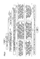
FIG. 3 is a flowchart of a pattern merge process performed by the pattern mergeunit 43 of thewrite testing unit 42 using the above three kinds of tables.FIG. 4 illustrates a concrete example of the pattern merge process. Referring toFIG. 3 , thetesting unit 40 reads the three tables of thepattern generating data 54d loaded and stored in the storage area (step S71). Specifically, the all-bit-no-write table 5a, the all-bit-write table 5b, and the user definition table 5c illustrated inFIG. 4 are read. - The
testing unit 40 then extracts all of the combinations of the values of LOT, WAF, and CHIP from the user definition table 5c included in thepattern generating data 54d (step S72). In the example ofFIG. 4 , the combinations of (LOT, WAF, CHIP) include (123, 10, 1), (123, 10, 2), and (234, 1, 2). Thetesting unit 40 reads thetest target information 51 stored in the storage area (step S72-2). Thetesting unit 40 compares the combinations of (LOT, WAF, CHIP) extracted in step S72 with thetest target information 51 read in step S72-2. If there is a combination having the corresponding item values, the routine proceeds to step S74 or step S74-2. If there is no corresponding combination, adefault pattern 5d is acquired from the user definition table 5c (step S73). - The selection of step S74 or step S74-2 corresponds to the selection of an all-
bits pattern 8a or a target-bits pattern 8b inFIG. 4 . Either step S74 or step S74-2 may be selected at the time of designing the program for the pattern merge process. Alternatively, the all-bits pattern 8a or the target-bits pattern 8b may be selected at the time of reading thetest target information 51 or thetest execution information 52 into thetesting apparatus 100. - First, a process of generating the all-
bits pattern 8a is described with reference to steps S74 and S75. Thetesting unit 40 acquires from the user definition table 5c a pattern with the item values corresponding to those of the combinations (LOT, WAF, CHIP) extracted in step S72. Thetesting unit 40 identifies the ADD of the combinations from the user definition table 5c having DEF "1" indicating write targets, and then extracts the write conditions for the combinations with the identified ADD from the all-bit-write table 5b (step S74). - For example, when the
test target information 51 designates lot No. 234, wafer No. 1, and chip No. 2, apattern 5s indicating the corresponding combinations (LOT=234, WAF=1, CHIP=2) is read from the user definition table 5c ofFIG. 4 . Then, ADDs "1" and "6" where DEF is "1" are identified. Then, the write conditions for the corresponding ADD "1" and "6" are extracted from the all-bit-write table 5b ofFIG. 4 . Specifically, the values of CYC and PGM are extracted from the all-bit-write table 5b ofFIG. 4 as the write conditions. More specifically, with regard to ADD "1" and "6", CYC "1 µs" and PGM "1" are extracted. - Thereafter, the
testing unit 40 modifies the item values of the all-bit-no-write table 5a with respect to the write target ADD, using the write conditions extracted in step S74, thereby generating the all-bits pattern 8a (step S75). Thus, with regard to ADD "1" and "6", the all-bits pattern 8a indicates CYC is "1 µs" and PGM is "1". The all-bits pattern 8a ofFIG. 4 is then outputted to a storage area for the write pattern data 44 (FIG. 1 ). - The
testing unit 40 then writes the all-bits pattern 8a stored in thewrite pattern data 44 in thePROM 23 of thechip 2 as thewrite pattern data 24 based on thetest target information 51, thereby completing the pattern merge process (step S78). - Next, a process of generating the target-
bits pattern 8b is described with reference to steps S74-2 and S75-2. Thetesting unit 40 acquires from the user definition table 5c a pattern with the item values corresponding to those of the combinations (LOT, WAF, CHIP) extracted in step S72. Then, the testing unit 40 (a) identifies the ADDs of the acquired combinations (write targets) indicating DEF "1", and extracts the write conditions for the identified ADDs from the all-bit-write table 5b; and (b) extracts the ADDs of no-write targets indicating DEF "0" (step S74-2). - Thus, in the example of
FIG. 4 , by the process (a), in the case where lot No. 234, wafer No. 1, and chip No. 2 are designated in thetest target information 51, thepattern 5s of the corresponding combination (LOT=234, WAF=1, CHIP=2) is read from the user definition table 5c ofFIG. 4 , and ADDs "1" and "6" indicating DEF "1" are identified as the write targets. Then, the write conditions for the target ADD "1" and "6" are extracted from the all-bit-write table 5b ofFIG. 4 . In this case, the values of CYC and PGM are extracted as the write conditions from the all-bit-write table 5b ofFIG. 4 . Specifically, regarding ADDs "1" and "6", CYC of "1 µs" and PGM of "1" are extracted. By the process (b), ADD "0", ADDs "2" through "5", and ADD "7", which all indicate DEF "0" in thepattern 5s, are extracted as the non-targets. - After the process of step S74-2, the
testing unit 40 modifies the item values of the all-bit-no-write table 5a with respect to the write target ADDs using the write conditions extracted in step S74-2, and deletes the bits corresponding to the write non-target ADDs (step S75-2). Namely, the all-bit-no-write table 5a ofFIG. 4 is modified such that CYC is "1 µs" and PGM is "1" with respect to ADDs "1" and "6", while the bits for ADD "0", ADDs "2" through "5", and ADD "7" are deleted, thereby producing the target-bits pattern 8b ofFIG. 4 . The target-bits pattern 8b is then outputted to a storage area for the write pattern data 44 (FIG. 1 ). - Based on the
test target information 51, thetesting unit 40 writes the target-bits pattern 8b stored in thewrite pattern data 44 in thePROM 23 of thechip 2 as thewrite pattern data 24, thereby completing the pattern merge process (step S78). - On the other hand, if it is determined in step S73 that there is no corresponding combination between the combinations (LOT, WAF, CHIP) extracted in step S72 and the
test target information 51 read in step S73, steps S76 and S77 are executed. In step S76, thetesting unit 40, using only the information of DEF and ADD from thedefault pattern 5d in the user definition table 5c, identifies the ADD of write targets with DEF "1", and extracts the corresponding write conditions from the all-bit-write table 5b. Specifically, from thedefault pattern 5d ofFIG. 4 , the ADDs "0", "2", "4", "5", and "6" of the write targets with DEF "1" are identified, and CYC "1 µs" and PGM "1" for the identified ADD are extracted from the all-bit-write table 5b. - Then, the
testing unit 40, using the write conditions extracted in step S76, modifies the item values of the all-bit-no-write table 5a with respect to the write target ADDs, thereby generating awrite default pattern 8c (step S77) such that CYC is "1 µs" and PGM is "1". Thewrite default pattern 8c ofFIG. 4 is then outputted to a storage area of the write pattern data 44 (FIG. 1 ). Based on thetest target information 51, thetesting unit 40 writes thewrite default pattern 8c stored in thewrite pattern data 44 in thePROM 23 of thechip 2 as thewrite pattern data 24, thereby completing the pattern merge process (step S78). -
FIG. 5 is a flowchart of an overall process performed by thetesting apparatus 100 including the above-described pattern merge process. Thetesting apparatus 100 reads thetest execution information 52 into the storage area using the test program activating unit 32 (step S11). Thetest execution information 52 includes theDC test program 53, theDC test pattern 53d, thewrite test program 54, and thepattern generating data 54d. - The
testing apparatus 100 also reads thetest target information 51 into the storage area using the test target information input unit 31 (step S12). Thetest target information 51 includes the designated lot number, wafer number, and chip number. - The
testing apparatus 100, by referring to a measurement map associating the chip number with the XY coordinates on the wafer, identifies the XY coordinates of the chip number on the wafer designated by thetest target information 51, and then causes thetesting unit 40 to perform a test (step S13). Specifically, in thetesting unit 40, first theDC testing unit 41 is activated by the execution of theDC test program 53 for thechip 2 designated by the XY coordinates, and the DC test is conducted for the chip 2 (step S14). Thereafter, thewrite test program 54 is executed, whereby thewrite testing unit 42 is activated and a write test is conducted for the chip 2 (step S15). - The write test conducted in step S15 is described. The
write testing unit 42 executes the pattern merge process as described above with reference toFIG. 3 based on the test target information 51 (step S15-1), thereby generating the write pattern data 44 (step S15-2). After a terminal setting for the chip 2 (step S15-3), a power supply setting (step S15-4), and a timing setting (step S15-5), thewrite testing unit 42 inputs thewrite pattern data 44 generated in step S15-2 into thePROM 23 of thechip 2 as the write pattern data 24 (step S15-6), and then a write test is executed within thechip 2. - Upon reception of a write test completion notice from the write testing unit 42 (step S16), the
testing unit 40 determines whether the test has been completed for all of the test target chips (step S17) based on thetest target information 51. If there is at least one chip that has not been tested, thetesting unit 40 repeats the above process for the chip from step S13. On the other hand, if all of the test target chips have been tested, the test process is completed. -
FIG. 6 is a block diagram of a hardware structure of thetesting apparatus 100. Thetesting apparatus 100, which may include a terminal controlled by a computer, includes a CPU (Central Processing Unit) 11, amemory unit 12, adisplay unit 13, anoutput unit 14, aninput unit 15, an interface (I/F) 16, astorage unit 17, and adriver 18, which are connected via a system bus B. - The
CPU 11 may be configured to control thetesting apparatus 100 in accordance with a program stored in thememory unit 12. Thememory unit 12, which may include a RAM (Random Access Memory) or a ROM (Read-Only Memory), may be configured to store the program executed by theCPU 11 and data required for or obtained by a process by theCPU 11. A part of thememory unit 12 may be allocated for a work area for a process performed by theCPU 11. - The
display unit 13 displays various information items under the control of theCPU 11. Theoutput unit 14 may include a printer and is used for outputting various information items in accordance with an instruction from a testing staff member. Theinput unit 15 may include a mouse and keyboard and is used for the input of various information items from the testing staff so that thetesting apparatus 100 can perform various processes. The I/F 16 enables connection via cable with a prober 16-2 on which awafer 200 is mounted. - The
storage unit 17, which may include a hard disk unit, stores programs and data for various processes. For example, the program for causing the CPU to provide the functions of the test targetinformation input unit 31, the testprogram activating unit 32, and thetesting unit 40 of thetesting apparatus 100 ofFIG. 1 is stored in thestorage unit 17. - A program for realizing the processes performed by the
testing apparatus 100 may be supplied to thetesting apparatus 100 via astorage medium 19, which may include a CD-ROM (Compact Disc Read-Only Memory). For example,
the CD-ROM is set on thedriver 18, and thedriver 18 reads the program from the CD-ROM and installs it in thestorage unit 17 via the system bus B. Upon start-up, theCPU 11 starts executing the program installed in thestorage unit 17. Such a storage medium is not limited to a CD-ROM and may include other computer-readable media. - The
test target information 51 inputted via theinput unit 15, for example, is stored in a storage area of thestorage unit 17 or thememory unit 12. Thetest execution information 52 may also be stored in a storage area of thestorage unit 17 or thememory unit 12 from thestorage medium 19 via thedriver 18. - The
testing apparatus 100 causes theDC testing unit 41 to perform a DC test on achip 2 of thewafer 200 mounted on the prober 16-2 in accordance with the chip number designated by thetest target information 51. After writing thewrite pattern data 44 in thechip 2, thetesting apparatus 100 causes thewrite testing unit 42 to perform a write test. - Thus, in accordance with the present embodiment, the
write pattern data 44 for thechip 2 on which an OTP memory, such as PROM, is implemented, is generated by thetesting apparatus 100. Thus, thechip 2 does not require the pattern generating circuit for generating the write pattern data. Thus, the man-hours for designing the pattern generating circuit and the area of macros can be reduced. - All examples and conditional language recited herein are intended for pedagogical purposes to aid the reader in understanding the invention and the concepts contributed by the inventor to furthering the art, and are to be construed as being without limitation to such specifically recited examples and conditions, nor does the organization of such examples in the specification relate to a showing of the superiority or inferiority of the invention.
- Although the embodiments of the present inventions have been described in detail, it should be understood that the various changes, substitutions, and alterations could be made hereto without departing from the spirit and scope of the invention.
Claims (10)
- An apparatus for testing a semiconductor integrated circuit, the apparatus comprising:a pattern data generating unit that generates test pattern data for testing a write operation in a memory of the semiconductor integrated circuit; anda write unit that writes the test pattern data into a storage area of the semiconductor integrated circuit.
- The apparatus according to claim 1, wherein the pattern data generating unit includes:an input unit that inputs test target information designating the semiconductor integrated circuit as a test target, and stores the test target information in a storage area of the apparatus;an operation-target-bit acquiring unit that acquires operation target bit information corresponding to the test target information stored in the storage area of the apparatus from a definition table, the definition table associating LSI-identifying information that identifies the semiconductor integrated circuit with bit-specifying information that specifies an operation target bit of the memory; anda merge unit that merges an operation condition for the operation target bit information which is acquired from an operation condition table that sets the operation condition for all of the bits of the memory, with a non-operation condition table that contains address information of all of the bits and in which a non-operation condition is set for all of the bits.
- The apparatus according to claim 1, wherein the pattern data generating unit includes:an input unit that inputs test target information designating the semiconductor integrated circuit as a test target, and stores the test target information in a storage area of the apparatus;an operation-target-bit acquiring unit that acquires operation target bit information corresponding to the test target information stored in the storage area of the apparatus from a definition table associating LSI-identifying information identifying the semiconductor integrated circuit with bit-specifying information specifying an operation target bit of the memory; anda merge unit that merges an operation condition for the operation target bit information which is acquired from an operation condition table in which the operation condition is set for all of the bits of the memory, with a non-operation condition table that contains address information of all of the bits and in which a non-operation condition is set for all of the bits,wherein the merge unit deletes data of one or more bits other than the operation target bits from the merged non-operation condition table.
- The apparatus according to claim 2 or 3, wherein the operation-target-bit acquiring unit acquires default target bit information from the definition table when the operation target bit corresponding to the test target information cannot be acquired from the definition table, and
the merge unit acquires from the operation condition table an operation condition corresponding to the default target bit information, and merges the operation condition corresponding to the default target bit information with the non-operation condition table. - The apparatus according to claim 4, wherein the pattern data generating unit generates the test pattern data for plural of the semiconductor integrated circuits.
- A method of testing a semiconductor integrated circuit by causing a computer to perform:generating test pattern data for testing a write operation in a memory of the semiconductor integrated circuit; andwriting the test pattern data into a storage area of the semiconductor integrated circuit.
- The method according to claim 6,
wherein the generating the test pattern data includes:inputting test target information designating the semiconductor integrated circuit as a test target into the computer;storing the test target information in a storage area of the computer;acquiring operation target bit information corresponding to the test target information stored in the storage area of the apparatus from a definition table, the definition table associating LSI-identifying information that identifies the semiconductor integrated circuit with bit-specifying information that specifies an operation target bit of the memory;acquiring an operation condition for the operation target bit information from an operation condition table in which an operation condition is set for all of the bits of the memory; andmerging the operation condition for the operation target bit with a non-operation condition table that contains address information of all of the bits and in which a non-operation condition is set for all of the bits. - A non-transitory computer-readable recording medium having a computer-executable program for causing a computer to function as an apparatus for testing a semiconductor integrated circuit,
the computer including:a first storage area in which test target information designating the semiconductor integrated circuit as a test target is stored; anda second storage area in which a non-operation condition table, an operation condition table, and a definition table are stored, wherein
the non-operation condition table includes address information of all of the bits of a memory of the semiconductor integrated circuit and sets a non-operation condition for all of the bits,
the operation condition table sets an operation condition for all of the bits, and
the definition table associates LSI-identifying information that identifies the semiconductor integrated circuit with bit-specifying information that specifies an operation target bit of the memory,the computer-executable program causing the computer to performacquiring operation target bit information corresponding to the test target information stored in the first storage area from the definition table;acquiring an operation condition for the operation target bit information from the operation condition table;merging the operation condition for the operation target bit information with the non-operation condition table in order to generate test pattern data; andwriting the test pattern data into a storage area of the semiconductor integrated circuit. - The recording medium according to claim 8, wherein the merging includes deleting data of one or more bits other than the operation target bits from the merged non-operation condition table.
- The recording medium according to claim 8, wherein the acquiring the operation target bit information includes acquiring default target bit information from the definition table when the operation target bit information corresponding to the test target information cannot be acquired from the definition table, and
the merging includes acquiring an operation condition for the default target bit information from the operation condition table, and merging the operation condition for the default target bit information with the non-operation condition table.
Applications Claiming Priority (1)
| Application Number | Priority Date | Filing Date | Title |
|---|---|---|---|
| JP2010051120A JP5477062B2 (en) | 2010-03-08 | 2010-03-08 | Semiconductor integrated circuit test apparatus, test method, and program |
Publications (2)
| Publication Number | Publication Date |
|---|---|
| EP2365488A1 true EP2365488A1 (en) | 2011-09-14 |
| EP2365488B1 EP2365488B1 (en) | 2016-10-19 |
Family
ID=43859808
Family Applications (1)
| Application Number | Title | Priority Date | Filing Date |
|---|---|---|---|
| EP11153138.0A Not-in-force EP2365488B1 (en) | 2010-03-08 | 2011-02-03 | Apparatus and method for testing semiconductor integrated circuits, and a non-transitory computer-readable medium having a semiconductor integrated circuit testing program |
Country Status (3)
| Country | Link |
|---|---|
| US (1) | US8656232B2 (en) |
| EP (1) | EP2365488B1 (en) |
| JP (1) | JP5477062B2 (en) |
Cited By (1)
| Publication number | Priority date | Publication date | Assignee | Title |
|---|---|---|---|---|
| CN107910036A (en) * | 2017-11-04 | 2018-04-13 | 上海华虹集成电路有限责任公司 | The test method of personalized MCU personalizations memory block |
Families Citing this family (2)
| Publication number | Priority date | Publication date | Assignee | Title |
|---|---|---|---|---|
| US20180137927A1 (en) * | 2016-04-16 | 2018-05-17 | Chengdu Haicun Ip Technology Llc | Three-Dimensional Vertical One-Time-Programmable Memory Comprising No Separate Diode Layer |
| JP2023136080A (en) * | 2022-03-16 | 2023-09-29 | キオクシア株式会社 | Memory system and information processing system |
Citations (5)
| Publication number | Priority date | Publication date | Assignee | Title |
|---|---|---|---|---|
| JPS5452933A (en) | 1977-10-04 | 1979-04-25 | Nec Corp | Writing device |
| US20030074153A1 (en) * | 2001-10-15 | 2003-04-17 | Shigeru Sugamori | Application specific event based semiconductor memory test system |
| JP2003196991A (en) | 2001-12-25 | 2003-07-11 | Fujitsu Ten Ltd | Rom write device |
| JP2004199827A (en) | 2002-12-20 | 2004-07-15 | Nec Access Technica Ltd | Data write-in device |
| US20050073332A1 (en) * | 2001-11-15 | 2005-04-07 | Kazuhiko Sato | Semiconductor testing apparatus |
Family Cites Families (23)
| Publication number | Priority date | Publication date | Assignee | Title |
|---|---|---|---|---|
| US4369511A (en) * | 1979-11-21 | 1983-01-18 | Nippon Telegraph & Telephone Public Corp. | Semiconductor memory test equipment |
| JPS6238600A (en) * | 1985-08-14 | 1987-02-19 | Fujitsu Ltd | Semiconductor memory device |
| JPH0432030A (en) * | 1990-05-29 | 1992-02-04 | Olympus Optical Co Ltd | Optical card recording and reproducing device |
| JP2940207B2 (en) * | 1991-04-12 | 1999-08-25 | 日本電気株式会社 | Compression pattern generation method |
| JPH0574199A (en) * | 1991-09-18 | 1993-03-26 | Fujitsu Ltd | Test data creation device and test data creation method |
| JPH05157802A (en) * | 1991-12-06 | 1993-06-25 | Mitsubishi Electric Corp | Semiconductor test equipment |
| JP2943521B2 (en) * | 1992-08-25 | 1999-08-30 | 松下電器産業株式会社 | Test vector generation method and test vector generation device |
| JP3819056B2 (en) * | 1994-09-01 | 2006-09-06 | テラダイン・インコーポレーテッド | Memory architecture for automated test equipment using vector module tables |
| JPH1183957A (en) * | 1997-09-09 | 1999-03-26 | Matsushita Electric Ind Co Ltd | Inspection device and inspection method |
| JPH11149795A (en) * | 1997-11-14 | 1999-06-02 | Ando Electric Co Ltd | Test pattern generation method of ic tester |
| US6161206A (en) * | 1998-04-30 | 2000-12-12 | Credence Systems Corporation | Pattern generator for a semiconductor integrated circuit tester |
| JP2001035191A (en) * | 1999-07-26 | 2001-02-09 | Mitsubishi Electric Corp | Verification pattern generation device, verification pattern generation method, and medium recording verification pattern generation program |
| JP2001155495A (en) * | 1999-11-29 | 2001-06-08 | Hitachi Ltd | Probe test apparatus and method |
| JP2001155497A (en) * | 1999-11-29 | 2001-06-08 | Hitachi Ltd | LSI test pattern program automatic generation method and apparatus, and LSI test method |
| JP2002022812A (en) * | 2000-07-06 | 2002-01-23 | Hitachi Electronics Eng Co Ltd | Pattern generator for semiconductor test equipment |
| JP3972089B2 (en) * | 2000-11-30 | 2007-09-05 | 株式会社ルネサステクノロジ | Semiconductor memory test board, test method, and manufacturing method |
| JP2003185715A (en) * | 2001-12-18 | 2003-07-03 | Hitachi Ltd | Inspection apparatus, inspection method, and method of manufacturing semiconductor device |
| JP4179827B2 (en) * | 2002-08-30 | 2008-11-12 | Necエレクトロニクス株式会社 | Memory test circuit |
| JP4451189B2 (en) * | 2004-04-05 | 2010-04-14 | 株式会社アドバンテスト | Test apparatus, phase adjustment method, and memory controller |
| JP4984438B2 (en) * | 2005-06-02 | 2012-07-25 | 富士通株式会社 | Memory test apparatus and memory test method |
| US7793175B1 (en) * | 2007-01-10 | 2010-09-07 | Marvell International Ltd. | Automated scan testing of DDR SDRAM |
| WO2008142004A1 (en) * | 2007-05-18 | 2008-11-27 | Xyratex Technology Limited | Apparatus and methods of generating a test pattern of data, analysing a test pattern of data, and testing a data storage disk medium and/or a read/write head |
| JP2009032313A (en) * | 2007-07-25 | 2009-02-12 | Toshiba Corp | Nonvolatile semiconductor memory device and method for testing nonvolatile semiconductor memory device |
-
2010
- 2010-03-08 JP JP2010051120A patent/JP5477062B2/en not_active Expired - Fee Related
-
2011
- 2011-02-02 US US13/019,831 patent/US8656232B2/en not_active Expired - Fee Related
- 2011-02-03 EP EP11153138.0A patent/EP2365488B1/en not_active Not-in-force
Patent Citations (5)
| Publication number | Priority date | Publication date | Assignee | Title |
|---|---|---|---|---|
| JPS5452933A (en) | 1977-10-04 | 1979-04-25 | Nec Corp | Writing device |
| US20030074153A1 (en) * | 2001-10-15 | 2003-04-17 | Shigeru Sugamori | Application specific event based semiconductor memory test system |
| US20050073332A1 (en) * | 2001-11-15 | 2005-04-07 | Kazuhiko Sato | Semiconductor testing apparatus |
| JP2003196991A (en) | 2001-12-25 | 2003-07-11 | Fujitsu Ten Ltd | Rom write device |
| JP2004199827A (en) | 2002-12-20 | 2004-07-15 | Nec Access Technica Ltd | Data write-in device |
Cited By (1)
| Publication number | Priority date | Publication date | Assignee | Title |
|---|---|---|---|---|
| CN107910036A (en) * | 2017-11-04 | 2018-04-13 | 上海华虹集成电路有限责任公司 | The test method of personalized MCU personalizations memory block |
Also Published As
| Publication number | Publication date |
|---|---|
| US8656232B2 (en) | 2014-02-18 |
| EP2365488B1 (en) | 2016-10-19 |
| JP2011187120A (en) | 2011-09-22 |
| JP5477062B2 (en) | 2014-04-23 |
| US20110219276A1 (en) | 2011-09-08 |
Similar Documents
| Publication | Publication Date | Title |
|---|---|---|
| CN113160875B (en) | Chip testing system and testing method | |
| US20030083855A1 (en) | Method for generating logic simulation model | |
| US8201037B2 (en) | Semiconductor integrated circuit and method for controlling semiconductor integrated circuit | |
| WO2020083367A1 (en) | Chip testing method, device, electronic apparatus and computer readable medium | |
| US20030120985A1 (en) | Method and apparatus for memory self testing | |
| KR102817444B1 (en) | Memory test apparatus and testing method thereof | |
| US12615096B2 (en) | Tester channel multiplexing in test equipment | |
| US8904247B2 (en) | Test pattern generation apparatus, test program generation apparatus, generation method, program, and test apparatus | |
| CN114333976A (en) | High-capacity flash memory chip testing method and device, electronic equipment and storage medium | |
| EP2365488B1 (en) | Apparatus and method for testing semiconductor integrated circuits, and a non-transitory computer-readable medium having a semiconductor integrated circuit testing program | |
| US10161999B1 (en) | Configurable system and method for debugging a circuit | |
| US20030237032A1 (en) | Method for electronically testing memory modules | |
| US11068369B2 (en) | Computer device and testing method for basic input/output system | |
| US9672094B1 (en) | Interconnect circuitry fault detection | |
| US7979762B2 (en) | Integrated circuit board with JTAG functions | |
| CN107068196A (en) | Built-in self-test circuit, system and method for flash memory | |
| CN115659883A (en) | Verification device and verification method for memory controller, storage medium and chip | |
| US6536020B2 (en) | Efficient generation of optimum test data | |
| CN119993249A (en) | A memory function test system and method | |
| US20130117610A1 (en) | Emulator verification system, emulator verification method | |
| US11971818B1 (en) | Memory view for non-volatile memory module | |
| US7986583B2 (en) | Method for designing integrated circuit incorporating memory macro | |
| CN118152311B (en) | Data processing method, device, system, electronic equipment and storage medium | |
| US11966633B1 (en) | Control algorithm generator for non-volatile memory module | |
| KR20220090928A (en) | Test method for system on chip and test system for system on chip |
Legal Events
| Date | Code | Title | Description |
|---|---|---|---|
| PUAI | Public reference made under article 153(3) epc to a published international application that has entered the european phase |
Free format text: ORIGINAL CODE: 0009012 |
|
| AK | Designated contracting states |
Kind code of ref document: A1 Designated state(s): AL AT BE BG CH CY CZ DE DK EE ES FI FR GB GR HR HU IE IS IT LI LT LU LV MC MK MT NL NO PL PT RO RS SE SI SK SM TR |
|
| AX | Request for extension of the european patent |
Extension state: BA ME |
|
| 17P | Request for examination filed |
Effective date: 20120228 |
|
| 17Q | First examination report despatched |
Effective date: 20130726 |
|
| RAP1 | Party data changed (applicant data changed or rights of an application transferred) |
Owner name: SOCIONEXT INC. |
|
| GRAP | Despatch of communication of intention to grant a patent |
Free format text: ORIGINAL CODE: EPIDOSNIGR1 |
|
| INTG | Intention to grant announced |
Effective date: 20160512 |
|
| RIN1 | Information on inventor provided before grant (corrected) |
Inventor name: GOMI, KENICHI Inventor name: TANEFUSA, YUSUKE Inventor name: YOKOO, SATOSHI |
|
| GRAS | Grant fee paid |
Free format text: ORIGINAL CODE: EPIDOSNIGR3 |
|
| GRAA | (expected) grant |
Free format text: ORIGINAL CODE: 0009210 |
|
| AK | Designated contracting states |
Kind code of ref document: B1 Designated state(s): AL AT BE BG CH CY CZ DE DK EE ES FI FR GB GR HR HU IE IS IT LI LT LU LV MC MK MT NL NO PL PT RO RS SE SI SK SM TR |
|
| REG | Reference to a national code |
Ref country code: GB Ref legal event code: FG4D |
|
| REG | Reference to a national code |
Ref country code: CH Ref legal event code: EP |
|
| REG | Reference to a national code |
Ref country code: AT Ref legal event code: REF Ref document number: 838942 Country of ref document: AT Kind code of ref document: T Effective date: 20161115 |
|
| REG | Reference to a national code |
Ref country code: IE Ref legal event code: FG4D |
|
| REG | Reference to a national code |
Ref country code: DE Ref legal event code: R096 Ref document number: 602011031361 Country of ref document: DE |
|
| REG | Reference to a national code |
Ref country code: NL Ref legal event code: MP Effective date: 20161019 |
|
| REG | Reference to a national code |
Ref country code: LT Ref legal event code: MG4D |
|
| PG25 | Lapsed in a contracting state [announced via postgrant information from national office to epo] |
Ref country code: LV Free format text: LAPSE BECAUSE OF FAILURE TO SUBMIT A TRANSLATION OF THE DESCRIPTION OR TO PAY THE FEE WITHIN THE PRESCRIBED TIME-LIMIT Effective date: 20161019 |
|
| REG | Reference to a national code |
Ref country code: AT Ref legal event code: MK05 Ref document number: 838942 Country of ref document: AT Kind code of ref document: T Effective date: 20161019 |
|
| PG25 | Lapsed in a contracting state [announced via postgrant information from national office to epo] |
Ref country code: GR Free format text: LAPSE BECAUSE OF FAILURE TO SUBMIT A TRANSLATION OF THE DESCRIPTION OR TO PAY THE FEE WITHIN THE PRESCRIBED TIME-LIMIT Effective date: 20170120 Ref country code: LT Free format text: LAPSE BECAUSE OF FAILURE TO SUBMIT A TRANSLATION OF THE DESCRIPTION OR TO PAY THE FEE WITHIN THE PRESCRIBED TIME-LIMIT Effective date: 20161019 Ref country code: NO Free format text: LAPSE BECAUSE OF FAILURE TO SUBMIT A TRANSLATION OF THE DESCRIPTION OR TO PAY THE FEE WITHIN THE PRESCRIBED TIME-LIMIT Effective date: 20170119 Ref country code: SE Free format text: LAPSE BECAUSE OF FAILURE TO SUBMIT A TRANSLATION OF THE DESCRIPTION OR TO PAY THE FEE WITHIN THE PRESCRIBED TIME-LIMIT Effective date: 20161019 |
|
| PG25 | Lapsed in a contracting state [announced via postgrant information from national office to epo] |
Ref country code: HR Free format text: LAPSE BECAUSE OF FAILURE TO SUBMIT A TRANSLATION OF THE DESCRIPTION OR TO PAY THE FEE WITHIN THE PRESCRIBED TIME-LIMIT Effective date: 20161019 Ref country code: FI Free format text: LAPSE BECAUSE OF FAILURE TO SUBMIT A TRANSLATION OF THE DESCRIPTION OR TO PAY THE FEE WITHIN THE PRESCRIBED TIME-LIMIT Effective date: 20161019 Ref country code: ES Free format text: LAPSE BECAUSE OF FAILURE TO SUBMIT A TRANSLATION OF THE DESCRIPTION OR TO PAY THE FEE WITHIN THE PRESCRIBED TIME-LIMIT Effective date: 20161019 Ref country code: PT Free format text: LAPSE BECAUSE OF FAILURE TO SUBMIT A TRANSLATION OF THE DESCRIPTION OR TO PAY THE FEE WITHIN THE PRESCRIBED TIME-LIMIT Effective date: 20170220 Ref country code: PL Free format text: LAPSE BECAUSE OF FAILURE TO SUBMIT A TRANSLATION OF THE DESCRIPTION OR TO PAY THE FEE WITHIN THE PRESCRIBED TIME-LIMIT Effective date: 20161019 Ref country code: RS Free format text: LAPSE BECAUSE OF FAILURE TO SUBMIT A TRANSLATION OF THE DESCRIPTION OR TO PAY THE FEE WITHIN THE PRESCRIBED TIME-LIMIT Effective date: 20161019 Ref country code: IS Free format text: LAPSE BECAUSE OF FAILURE TO SUBMIT A TRANSLATION OF THE DESCRIPTION OR TO PAY THE FEE WITHIN THE PRESCRIBED TIME-LIMIT Effective date: 20170219 Ref country code: BE Free format text: LAPSE BECAUSE OF FAILURE TO SUBMIT A TRANSLATION OF THE DESCRIPTION OR TO PAY THE FEE WITHIN THE PRESCRIBED TIME-LIMIT Effective date: 20161019 Ref country code: NL Free format text: LAPSE BECAUSE OF FAILURE TO SUBMIT A TRANSLATION OF THE DESCRIPTION OR TO PAY THE FEE WITHIN THE PRESCRIBED TIME-LIMIT Effective date: 20161019 Ref country code: AT Free format text: LAPSE BECAUSE OF FAILURE TO SUBMIT A TRANSLATION OF THE DESCRIPTION OR TO PAY THE FEE WITHIN THE PRESCRIBED TIME-LIMIT Effective date: 20161019 |
|
| REG | Reference to a national code |
Ref country code: DE Ref legal event code: R097 Ref document number: 602011031361 Country of ref document: DE |
|
| PG25 | Lapsed in a contracting state [announced via postgrant information from national office to epo] |
Ref country code: CZ Free format text: LAPSE BECAUSE OF FAILURE TO SUBMIT A TRANSLATION OF THE DESCRIPTION OR TO PAY THE FEE WITHIN THE PRESCRIBED TIME-LIMIT Effective date: 20161019 Ref country code: SK Free format text: LAPSE BECAUSE OF FAILURE TO SUBMIT A TRANSLATION OF THE DESCRIPTION OR TO PAY THE FEE WITHIN THE PRESCRIBED TIME-LIMIT Effective date: 20161019 Ref country code: RO Free format text: LAPSE BECAUSE OF FAILURE TO SUBMIT A TRANSLATION OF THE DESCRIPTION OR TO PAY THE FEE WITHIN THE PRESCRIBED TIME-LIMIT Effective date: 20161019 Ref country code: EE Free format text: LAPSE BECAUSE OF FAILURE TO SUBMIT A TRANSLATION OF THE DESCRIPTION OR TO PAY THE FEE WITHIN THE PRESCRIBED TIME-LIMIT Effective date: 20161019 Ref country code: DK Free format text: LAPSE BECAUSE OF FAILURE TO SUBMIT A TRANSLATION OF THE DESCRIPTION OR TO PAY THE FEE WITHIN THE PRESCRIBED TIME-LIMIT Effective date: 20161019 |
|
| PLBE | No opposition filed within time limit |
Free format text: ORIGINAL CODE: 0009261 |
|
| STAA | Information on the status of an ep patent application or granted ep patent |
Free format text: STATUS: NO OPPOSITION FILED WITHIN TIME LIMIT |
|
| PG25 | Lapsed in a contracting state [announced via postgrant information from national office to epo] |
Ref country code: SM Free format text: LAPSE BECAUSE OF FAILURE TO SUBMIT A TRANSLATION OF THE DESCRIPTION OR TO PAY THE FEE WITHIN THE PRESCRIBED TIME-LIMIT Effective date: 20161019 Ref country code: IT Free format text: LAPSE BECAUSE OF FAILURE TO SUBMIT A TRANSLATION OF THE DESCRIPTION OR TO PAY THE FEE WITHIN THE PRESCRIBED TIME-LIMIT Effective date: 20161019 Ref country code: BG Free format text: LAPSE BECAUSE OF FAILURE TO SUBMIT A TRANSLATION OF THE DESCRIPTION OR TO PAY THE FEE WITHIN THE PRESCRIBED TIME-LIMIT Effective date: 20170119 |
|
| 26N | No opposition filed |
Effective date: 20170720 |
|
| PG25 | Lapsed in a contracting state [announced via postgrant information from national office to epo] |
Ref country code: MC Free format text: LAPSE BECAUSE OF FAILURE TO SUBMIT A TRANSLATION OF THE DESCRIPTION OR TO PAY THE FEE WITHIN THE PRESCRIBED TIME-LIMIT Effective date: 20161019 |
|
| REG | Reference to a national code |
Ref country code: CH Ref legal event code: PL |
|
| GBPC | Gb: european patent ceased through non-payment of renewal fee |
Effective date: 20170203 |
|
| PG25 | Lapsed in a contracting state [announced via postgrant information from national office to epo] |
Ref country code: CH Free format text: LAPSE BECAUSE OF NON-PAYMENT OF DUE FEES Effective date: 20170228 Ref country code: LI Free format text: LAPSE BECAUSE OF NON-PAYMENT OF DUE FEES Effective date: 20170228 |
|
| REG | Reference to a national code |
Ref country code: IE Ref legal event code: MM4A |
|
| PG25 | Lapsed in a contracting state [announced via postgrant information from national office to epo] |
Ref country code: SI Free format text: LAPSE BECAUSE OF FAILURE TO SUBMIT A TRANSLATION OF THE DESCRIPTION OR TO PAY THE FEE WITHIN THE PRESCRIBED TIME-LIMIT Effective date: 20161019 |
|
| REG | Reference to a national code |
Ref country code: FR Ref legal event code: ST Effective date: 20171031 |
|
| PG25 | Lapsed in a contracting state [announced via postgrant information from national office to epo] |
Ref country code: LU Free format text: LAPSE BECAUSE OF NON-PAYMENT OF DUE FEES Effective date: 20170203 |
|
| PG25 | Lapsed in a contracting state [announced via postgrant information from national office to epo] |
Ref country code: FR Free format text: LAPSE BECAUSE OF NON-PAYMENT OF DUE FEES Effective date: 20170228 |
|
| PG25 | Lapsed in a contracting state [announced via postgrant information from national office to epo] |
Ref country code: GB Free format text: LAPSE BECAUSE OF NON-PAYMENT OF DUE FEES Effective date: 20170203 Ref country code: IE Free format text: LAPSE BECAUSE OF NON-PAYMENT OF DUE FEES Effective date: 20170203 |
|
| PGFP | Annual fee paid to national office [announced via postgrant information from national office to epo] |
Ref country code: DE Payment date: 20180123 Year of fee payment: 8 |
|
| PG25 | Lapsed in a contracting state [announced via postgrant information from national office to epo] |
Ref country code: MT Free format text: LAPSE BECAUSE OF NON-PAYMENT OF DUE FEES Effective date: 20170203 |
|
| PG25 | Lapsed in a contracting state [announced via postgrant information from national office to epo] |
Ref country code: HU Free format text: LAPSE BECAUSE OF FAILURE TO SUBMIT A TRANSLATION OF THE DESCRIPTION OR TO PAY THE FEE WITHIN THE PRESCRIBED TIME-LIMIT; INVALID AB INITIO Effective date: 20110203 |
|
| REG | Reference to a national code |
Ref country code: DE Ref legal event code: R119 Ref document number: 602011031361 Country of ref document: DE |
|
| PG25 | Lapsed in a contracting state [announced via postgrant information from national office to epo] |
Ref country code: CY Free format text: LAPSE BECAUSE OF NON-PAYMENT OF DUE FEES Effective date: 20161019 |
|
| PG25 | Lapsed in a contracting state [announced via postgrant information from national office to epo] |
Ref country code: MK Free format text: LAPSE BECAUSE OF FAILURE TO SUBMIT A TRANSLATION OF THE DESCRIPTION OR TO PAY THE FEE WITHIN THE PRESCRIBED TIME-LIMIT Effective date: 20161019 |
|
| PG25 | Lapsed in a contracting state [announced via postgrant information from national office to epo] |
Ref country code: DE Free format text: LAPSE BECAUSE OF NON-PAYMENT OF DUE FEES Effective date: 20190903 |
|
| PG25 | Lapsed in a contracting state [announced via postgrant information from national office to epo] |
Ref country code: TR Free format text: LAPSE BECAUSE OF FAILURE TO SUBMIT A TRANSLATION OF THE DESCRIPTION OR TO PAY THE FEE WITHIN THE PRESCRIBED TIME-LIMIT Effective date: 20161019 |
|
| PG25 | Lapsed in a contracting state [announced via postgrant information from national office to epo] |
Ref country code: AL Free format text: LAPSE BECAUSE OF FAILURE TO SUBMIT A TRANSLATION OF THE DESCRIPTION OR TO PAY THE FEE WITHIN THE PRESCRIBED TIME-LIMIT Effective date: 20161019 |