EP2356737B1 - Leistungsschaltung - Google Patents
Leistungsschaltung Download PDFInfo
- Publication number
- EP2356737B1 EP2356737B1 EP08878800.5A EP08878800A EP2356737B1 EP 2356737 B1 EP2356737 B1 EP 2356737B1 EP 08878800 A EP08878800 A EP 08878800A EP 2356737 B1 EP2356737 B1 EP 2356737B1
- Authority
- EP
- European Patent Office
- Prior art keywords
- value
- switching device
- kcdv
- current
- cdv
- Prior art date
- Legal status (The legal status is an assumption and is not a legal conclusion. Google has not performed a legal analysis and makes no representation as to the accuracy of the status listed.)
- Active
Links
Images


Classifications
-
- H—ELECTRICITY
- H02—GENERATION; CONVERSION OR DISTRIBUTION OF ELECTRIC POWER
- H02M—APPARATUS FOR CONVERSION BETWEEN AC AND AC, BETWEEN AC AND DC, OR BETWEEN DC AND DC, AND FOR USE WITH MAINS OR SIMILAR POWER SUPPLY SYSTEMS; CONVERSION OF DC OR AC INPUT POWER INTO SURGE OUTPUT POWER; CONTROL OR REGULATION THEREOF
- H02M1/00—Details of apparatus for conversion
- H02M1/44—Circuits or arrangements for compensating for electromagnetic interference in converters or inverters
-
- H—ELECTRICITY
- H02—GENERATION; CONVERSION OR DISTRIBUTION OF ELECTRIC POWER
- H02H—EMERGENCY PROTECTIVE CIRCUIT ARRANGEMENTS
- H02H1/00—Details of emergency protective circuit arrangements
- H02H1/04—Arrangements for preventing response to transient abnormal conditions, e.g. to lightning or to short duration over voltage or oscillations; Damping the influence of DC component by short circuits in AC networks
-
- H—ELECTRICITY
- H02—GENERATION; CONVERSION OR DISTRIBUTION OF ELECTRIC POWER
- H02H—EMERGENCY PROTECTIVE CIRCUIT ARRANGEMENTS
- H02H3/00—Emergency protective circuit arrangements for automatic disconnection directly responsive to an undesired change from normal electric working condition with or without subsequent reconnection ; integrated protection
- H02H3/02—Details
- H02H3/05—Details with means for increasing reliability, e.g. redundancy arrangements
-
- H—ELECTRICITY
- H02—GENERATION; CONVERSION OR DISTRIBUTION OF ELECTRIC POWER
- H02H—EMERGENCY PROTECTIVE CIRCUIT ARRANGEMENTS
- H02H7/00—Emergency protective circuit arrangements specially adapted for specific types of electric machines or apparatus or for sectionalised protection of cable or line systems, and effecting automatic switching in the event of an undesired change from normal working conditions
- H02H7/26—Sectionalised protection of cable or line systems, e.g. for disconnecting a section on which a short-circuit, earth fault, or arc discharge has occured
Definitions
- the present invention relates generally to the field of power circuitry. More particularly, the present invention relates generally to controlling circuit components during power disturbances.
- a plurality of sub-systems may be coupled to a system.
- the plurality of sub-systems may share a power bus and, therefore, the power received at each sub-system may be directly correlated to power conditions at other sub-systems. Accordingly, an event at one sub-system may cause a power disturbance at another sub-system. This may have a negative effect on the operation of a sub-system not associated with the event.
- Various embodiments provide systems and methods for controlling sub-system components during power disturbances. More particularly, various embodiments provide a system and method for preventing a controller within a sub-system from turning OFF a switching device during power disturbance events related to other sub-systems. Such protective controllers are for example disclosed in patent application US20080150369 .
- Various embodiments provide an apparatus and methods for measuring a + dv/dt value above a predetermined threshold; scaling the + dv/dt value by a capacitance (C) value to produce a + Cdv/dt value; scaling the + Cdv/dt value based on a gain (K) of a current sensing component to produce a + KCdv/dt value; and subtracting the + KCdv/dt value from an increased current associated with a power disturbance.
- C capacitance
- K gain
- Various embodiments also provide an apparatus comprising a circuit for receiving a + Cdv/dt value, the circuit configured to determine if a current level or a voltage level associated with the + Cdv/dt value is greater than a predetermined threshold and output a signal to a switching device if the current level or the voltage level associated with the + Cdv/dt value is greater than a predetermined threshold, wherein the signal causes the switching device to switch to an OFF state.
- Various embodiments provide systems and methods for controlling sub-system components during power disturbances. More particularly, various embodiments provide a circuit and method for preventing a controller within a sub-system from turning OFF a switching device during power disturbance events related to other sub-systems.
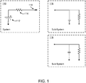
- FIG. 1 illustrates an exemplary system 110 of the present application.
- the system 110 may be a system enclosure, a card cage, a main system, a cabinet, or similar structures.
- the system is modeled as a Thevenin equivalent comprising a power source 112 and a series resistor 114.
- the system 110 is actually more complex and comprises a plurality of components arranged in a specific manner to interconnect with and provide power to various sub-systems 118. These sub-systems 118 are interconnected with the system 110 via one or more connectors 116.
- the system 110 is arranged such that one or more sub-systems may be inserted or otherwise coupled to the system 110.
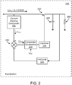
- Figure 2 illustrates an exemplary implementation of various embodiments of the present application. More particularly, Figure 2 illustrates a sub-system 210 configured to be interconnected with system 110 or inserted therein. Although only one sub-system 210 is illustrated, there may be one or more sub-systems electronically coupled with the system 110. As described herein, the sub-system 210 may be a sub-assembly, an add-in-card, a cell, a board, or similar structures. Accordingly, a system 110, such as a card cage or cabinet, may include one or more sub-systems, such as a card or blade.
- Each sub-system 210 of the present application includes a circuitry arrangement which prevents a controller 215 from turning OFF a switching device 220 in response to a positive increased current ( + Cdv/dt).
- the increased current ( + Cdv/dt) may occur due to a fault condition at another sub-system, a sub-system insertion, or another event which may raise the positive current provided to sub-system 210.
- Figure 2 illustrates an exemplary embodiment of the present application which prevents a controller 215 from turning OFF a switching device 220 when an increased current ( + Cdv/dt) is received at sub-system 210.
- the switching device 220 may be a MOSFET, a PNP transistor, NPN transistor, or similar switching structures.
- the controller 215 may be an electronic-fuse (e-fuse) controller, a hot swap controller, or other similar controlling structures.
- a power disturbance may occur at sub-system 210.
- This power disturbance may take the form of an increased current ( + Cdv/dt) being received at sub-system 210.
- the increased current ( + Cdv/dt) is combined with the normal operating current (I L ) to a load 260, a total current (I TOTAL ) is produced which is higher than the normal operating current.
- the total current (I TOTAL ) during a power disturbance may be problematic to sub-system 210.
- the total current (I TOTAL ) may be sensed by a current sensing component 230 and thereby trigger controller 215 to turn OFF switching device 220. More specifically, the total current (I TOTAL ) may cause the current sensing component 230 to output an increased voltage V1 OUT directly to the comparator component 240 in response to the power disturbance.
- the current sensing component 230 may be a current sensing amplifier, a resistor, a Hall effect sensor, a current transformer, or similar current sensing structures.
- V1 OUT (which is a higher value than normal)
- V1 OUT determines that V1 OUT is greater than V1 REF and sends an indication to controller 215 instructing the controller 215 to turn OFF switching device 220.
- V1 OUT must be reduced before being received at the comparator component 240. As illustrated in Figure 2 , this may be accomplished by removing or subtracting a scaled + Cdv/dt component 245 from V1 OUT . If the scaled + Cdv/dt component 245 is properly subtracted from V1 OUT , V1 MOD is produced.
- V1 MOD has a value which, when compared with V1 REF , does not trigger the comparator component 240 to send an indication to the controller 215 instructing the controller 215 to turn OFF switching device 220.
- Sub-system 210 is arranged to produce a scaled + Cdv/dt value 245 which is subtracted from V1 OUT prior to being received by comparator component 240.
- the details of scaling the + Cdv/dt are described in greater detail below with reference to Figure 3 .
- the scaled + Cdv/dt value 245 is subtracted from V1 OUT via subtractor 250.
- the subtractor 250 may be a component configured to subtract two values. Alternatively, the subtracting 250 may be a junction in the circuit.
- R SENSE is a resistance associated with the current sensing component 230. Accordingly, the + Cdv/dt current caused by the power disturbance is essentially not apparent in V1 MOD . Therefore, when V1 MOD is compared by the comparator component 240 against V1 REF , the result may be substantially zero. As such, the comparator component 240 will not instruct the controller 215 to turn OFF the switching device 220. It is noted that the when V1 MOD is compared by the comparator 240, the result does not have to be substantially zero. Instead, the result may be any value that creates an output from the comparator 240 which does not cause the controller 215 to turn OFF the switching device 220.
- comparator component 240 and the controller 215 are discussed and illustrated as two separate components, the comparator component 240 and the controller 215 do not have to be separate.
- the comparator component 240 and the controller 215 may be part of a single component or a single integrated circuit.
- the subtraction operation is not limited to the location illustrated in Figure 2 . Instead, the subtraction operation may occur at a different junction.
- the subtractor 250 may be located prior to the current sensing component 230.
- a scaled + Cdv/dt value 245 is subtracted from I TOTAL prior to being sensed by the current sensing component 230.
- the current sensing component 230 receives a current which does not include the increased current ( + Cdv/dt) caused by the voltage disturbance at another sub-system. Accordingly, the voltage output by the current sensing component 230 to the comparator component 240 will not be an increased value and, therefore, the comparator component 240 will not trigger the controller 215 to turn OFF the switching device 220.
- Figure 3 illustrates an exemplary embodiment for producing the scaled + Cdv/dt value 245.
- This circuit is for exemplary purposes only and should not be seen as limiting, as other arrangements for producing the scaled + Cdv/dt value 245 may also be used.
- a differentiator circuit 301 may be used to sample a voltage (V2) and output a + Cdv/dt value. More particularly, the differentiator circuit 301 may sample voltage (V2) from a point on sub-system 210 or a point on system 110. Based on the sampled voltage (V2), the differentiator circuit 301 determines a + dv/dt value.
- This + dv/dt value may be scaled by the differentiator circuit 301 based on a capacitance (C) at the output of the controller 215.
- the + dv/dt value may be scaled based on the capacitance at capacitor 225.
- the differentiator circuit 301 produces a + Cdv/dt value.
- the differentiator circuit is configured to only scale + dv/dt values above a predetermined threshold. That is, nominal or other low + dv/dt values (below the predetermined threshold), which may be present in normal operating conditions, are not output from differentiator circuit 301.
- the differentiator circuit 301 is configured to output + Cdv/dt values above a predetermined threshold which may be caused by power disturbances.
- An exemplary differentiator circuit 301 may comprise a capacitor, an op-amp, a diode, and a resistor.
- the differentiator circuit 301 outputs + Cdv/dt to a scaling and/or inverting circuit 302.
- the scaling and/or inverting circuit 302 may scale the + Cdv/dt by a scaling value (K).
- K may be a gain value based on the above-discussed current sensing component 230.
- the scaling and/or inverting circuit 302 may also invert the scaled + Cdv/dt value. This inversion is dependent upon the arrangement and location of the subtractor 250.
- the output of the scaling and/or inverting circuit 302 is +/- KCdv/dt. As discussed above, this +/- KCdv/dt value is subtracted from V1 OUT or I TOTAL , thereby presenting the comparator 240 with a voltage that does not trigger the controller 215 to turn OFF switching device 220.
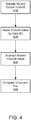
- FIG. 4 is an flow chart illustrating exemplary implementations of various embodiments.
- a differentiator circuit samples a voltage (V2) and outputs a + Cdv/dt value.
- V2 the + Cdv/dt value is scaled by a gain value K.
- the scaled + Cdv/dt value is subtracted from V1 OUT thereby removing the + Cdv/dt component from V1 OUT and producing V1 MOD .
- V1 MOD is compared by the comparator 240 against V REF . This comparison produces an output from the comparator 240 which does not trigger the controller 215 to turn OFF switching device 220.
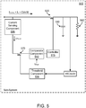
- Figure 5 illustrates another exemplary embodiment of the present application which prevents a controller 515 from turning OFF a switching device 520 when an increased current ( + Cdv/dt) is received at sub-system 510.
- power disturbance events related to other sub-systems may cause an increased in current ( + Cdv/dt) and thereby increase the value of V1 OUT .
- This increased value of V1 OUT may cause the comparator component 540 to instruct the controller 515 to turn OFF switching device 520 due to V1 OUT exceeding V REF .
- various embodiments provide a threshold component 550 configured to receive + Cdv/dt or + KCdv/dt, as defined above.
- the + Cdv/dt or + KCdv/dt may be received in the same manner as described with respect to Figure 3 .
- the threshold component 550 may be a voltage amplifier or other similar structures configured to determine if a voltage is exceeded.
- the threshold component 550 determines if a predetermined threshold, e.g., a threshold value close to V REF , is exceeded. If the threshold component 550 detects that the predetermined threshold is exceeded, the threshold component 550 is configured to output a signal to a switching device 570 to turn OFF the switching device 570. As such, V1 OUT is not received at the comparator component 540.
- the comparator component 540 is blocked from determining that V1 OUT exceeds V REF during power disturbances, and the comparator component 540 does not instruct the controller 515 to turn OFF switching device 520.
- the switching device 570 may be a MOSFET, a PNP transistor, NPN transistor, or similar switching structures.
- the threshold component 550 is not limited to measuring voltages.
- the threshold component 550 may also measure current. This may be done by using, for example, a current amplifier.
- the threshold component 550 may sample + Cdv/dt or + KCdv/dt and determine if a current threshold is breached. If so, the threshold component 550 may send a signal to the a switching device 570 to turn OFF, thereby blocking V1 OUT from being received at the comparator component 540. Accordingly, the comparator component 540 is blocked from determining that V1 OUT exceeds V REF and, therefore, does not instruct the controller 515 to turn OFF switching device 520.
- FIG. 6 is an flow chart illustrating exemplary implementations of various embodiments.
- a + Cdv/dt or + KCdv/dt value is obtained by a threshold component 550.
- the threshold component determines if + Cdv/dt or + KCdv/dt exceeds a voltage or current threshold.
- the threshold component 550 continues monitoring + Cdv/dt or + KCdv/dt.
- the threshold component 550 outputs a signal to a switching device 570 causing the switching device to turn OFF.
- the comparator component 540 is blocked from determining that V1 OUT exceeds V REF . Therefore, the comparator component 540 does not instruct the controller 515 to turn OFF switching device 520.
Landscapes
- Engineering & Computer Science (AREA)
- Power Engineering (AREA)
- Physics & Mathematics (AREA)
- Electromagnetism (AREA)
- Power Conversion In General (AREA)
- Electronic Switches (AREA)
Claims (11)
- Vorrichtung, welche umfasst:ein Bauteil zur Strommessung (230, 531),einen Schaltkreis (301) zur Messung eines +dv/dt-Werts über einem vorgegebenen Schwellenwert und Skalierung des +dv/dt-Werts durch einen Kapazitätswert (C) zur Erzeugung eines +Cdv/dt-Werts;einen Schaltkreis (302) zur Skalierung des +Cdv/dt-Werts auf Grundlage des Gewinns (K) eines Bauteils zur Strommessung (230) zur Erzeugung eines +KCdv/dt-Werts; undgekennzeichnet dadurch, dass:a) die Vorrichtung überdies einen Schaltkreis (250) für Subtrahieren des +KCdv/dt-Werts von der aktuellen Messgröße von dem Messbauteil (230) umfasst, assoziiert mit Netzstörung, wobei Subtrahieren des +KCdv/dt-Werts von der aktuellen Messgröße einen Schaltgerätregler (215) veranlasst, ein erstes Schaltgerät (220) in einem EIN-Status aufrechtzuerhalten; oderb) die Vorrichtung überdies einen Schaltkreis zum Empfangen des +KCdv/dt-Werts umfasst, wobei der Schaltkreis ausgestaltet ist, festzulegen, ob ein Stromniveau oder Spannungsniveau, das mit dem +KCdv/dt-Wert assoziiert ist, größer ist als ein vorgegebener Schwellenwert, und ein Signal an ein zweites Schaltgerät (570) auszugeben, wenn das Stromniveau oder das Spannungsniveau, das mit dem +KCdv/dt-Wert assoziiert ist, größer ist als ein vorgegebener Schwellenwert, wobei das Signal das zweite Schaltgerät (570) veranlasst, in einen AUS-Status zu schalten, was verhindert, dass der Schaltgerätregler (515) das erste Schaltgerät (520) in den AUS-Status ändert.
- Vorrichtung nach Anspruch 1, wobei die Vorrichtung ein Subsystem (210) umfasst, das mit einem System (110) assoziiert ist.
- Vorrichtung nach Anspruch 2, wobei die Netzstörung mit einem anderen Subsystem assoziiert ist, das mit dem System (110) assoziiert ist.
- Vorrichtung nach Anspruch 1, wobei der Kapazitätswert (C) auf einer Kapazität bei einer Ausgabe des ersten Schaltgerätreglers (215) basiert.
- Verfahren, welches umfasst:Messen eines +dv/dt-Werts über einem vorgegebenen Schwellenwert;Skalierung des +dv/dt-Werts durch einen Kapazitätswert (C) zur Erzeugung eines +Cdv/dt-Werts;Skalierung des +Cdv/dt-Werts auf Grundlage des Gewinns (K) eines Bauteils zur Strommessung (230) zur Erzeugung eines +KCdv/dt-Werts;gekennzeichnet dadurch, dass:a) das Verfahren überdies Subtrahieren des +KCdv/dt-Werts von einer Strommessgröße, assoziiert mit einer Netzstörung, umfasst, wobei Subtrahieren des +KCdv/dt-Werts von der Strommessgröße einen Schaltgerätregler (215) veranlasst, ein erstes Schaltgerät (220) in einem EIN-Status aufrechtzuerhalten; oderb) das Verfahren überdies Bestimmen, durch einen Schaltkreis, in dem der +KCdv/dt-Wert empfangen wird, ob ein Stromniveau oder Spannungsniveau, das mit dem +KCdv/dt-Wert assoziiert ist, größer ist als ein vorgegebener Schwellenwert, und Ausgeben eines Signals an ein zweites Schaltgerät (570), wenn das Stromniveau oder das Spannungsniveau, das mit dem +KCdv/dt-Wert assoziiert ist, größer ist als ein vorgegebener Schwellenwert, umfasst, wobei das Signal das zweite Schaltgerät (570) veranlasst, in einen AUS-Status zu schalten, was verhindert, dass der Schaltgerätregler (515) das erste Schaltgerät (520) in den AUS-Status ändert.
- Verfahren nach Anspruch 5, wobei die Prozesse des Messens des +dv/dt-Werts und des Skalierens des +dv/dt-Werts von einem Differentiator-Schaltkreis (301) durchgeführt werden.
- Verfahren nach Anspruch 5, wobei als Reaktion auf Subtrahieren des +KCdv/dt-Werts vom erhöhten Strom, assoziiert mit der Netzstörung, ein Komparator-Bauteil (240) mit einem Spannungsniveau präsentiert wird, das verglichen mit einer Referenzspannung das Komparator-Bauteil (240) veranlasst, ein Signal auszugeben, das einen Schaltgerätregler (215) anweist, ein Schaltgerät (220) in einem EIN-Status aufrechtzuerhalten.
- Vorrichtung nach Anspruch 1, wobei der +Cdv/dt-Wert größer ist als der vorgegebene Schwellenwert unter Netzstörungsbedingungen.
- Vorrichtung nach Anspruch 8, wobei Schalten des zweiten Schaltgeräts (570) in einen AUS-Status verhindert, dass eine Spannung bei einem Komparator (540) empfangen wird.
- Vorrichtung nach Anspruch 1, wobei der Schaltkreisregler (215, 515) ein Elektro-Sicherungs-Regler oder ein Hot-Swap-Regler ist.
- Vorrichtung nach Anspruch 1, wobei der vorgegebene Schwellenwert gleich oder geringer als eine Referenzspannung eines Komparators (540) ist.
Applications Claiming Priority (1)
| Application Number | Priority Date | Filing Date | Title |
|---|---|---|---|
| PCT/US2008/086083 WO2010068197A1 (en) | 2008-12-09 | 2008-12-09 | Power circuit |
Publications (3)
| Publication Number | Publication Date |
|---|---|
| EP2356737A1 EP2356737A1 (de) | 2011-08-17 |
| EP2356737A4 EP2356737A4 (de) | 2017-05-10 |
| EP2356737B1 true EP2356737B1 (de) | 2018-02-28 |
Family
ID=42242971
Family Applications (1)
| Application Number | Title | Priority Date | Filing Date |
|---|---|---|---|
| EP08878800.5A Active EP2356737B1 (de) | 2008-12-09 | 2008-12-09 | Leistungsschaltung |
Country Status (4)
| Country | Link |
|---|---|
| US (1) | US8975902B2 (de) |
| EP (1) | EP2356737B1 (de) |
| CN (1) | CN102246402B (de) |
| WO (1) | WO2010068197A1 (de) |
Families Citing this family (1)
| Publication number | Priority date | Publication date | Assignee | Title |
|---|---|---|---|---|
| JP2021096089A (ja) * | 2019-12-13 | 2021-06-24 | 株式会社東芝 | 電圧変化率検出回路、半導体装置及び電力変換器 |
Family Cites Families (18)
| Publication number | Priority date | Publication date | Assignee | Title |
|---|---|---|---|---|
| JP2868422B2 (ja) * | 1993-10-28 | 1999-03-10 | ヴィエルティー コーポレーション | 電力変換における電流検出装置及び方法 |
| JP3655378B2 (ja) | 1995-11-28 | 2005-06-02 | ファナック株式会社 | サーボモータの外乱負荷推定方法 |
| US5890097A (en) | 1997-03-04 | 1999-03-30 | Eaton Corporation | Apparatus for waveform disturbance monitoring for an electric power system |
| US6026458A (en) * | 1997-10-14 | 2000-02-15 | International Business Machines Corporation | System with pluggable adapter card and hot-swap interface controller |
| US6917504B2 (en) * | 2001-05-02 | 2005-07-12 | Supertex, Inc. | Apparatus and method for adaptively controlling power supplied to a hot-pluggable subsystem |
| US6950950B2 (en) * | 2001-12-28 | 2005-09-27 | Hewlett-Packard Development Company, L.P. | Technique for conveying overload conditions from an AC adapter to a load powered by the adapter |
| US6670821B2 (en) * | 2002-01-02 | 2003-12-30 | Broadcom Corporation | Methods and systems for sensing and compensating for process, voltage, temperature, and load variations |
| US6975098B2 (en) * | 2002-01-31 | 2005-12-13 | Vlt, Inc. | Factorized power architecture with point of load sine amplitude converters |
| JP2003289620A (ja) * | 2002-03-27 | 2003-10-10 | Fujitsu Ltd | 突入電流抑制装置 |
| US20040070908A1 (en) * | 2002-09-27 | 2004-04-15 | International Business Machines Corporation | Overcurrent protection of input/output devices in a data processing system |
| US7061301B2 (en) * | 2003-12-19 | 2006-06-13 | Power Integrations, Inc. | Method and apparatus switching a semiconductor switch with a multi-state drive circuit |
| US7542258B2 (en) * | 2004-01-16 | 2009-06-02 | Lutron Electronics Co., Inc. | DV/dt-detecting overcurrent protection circuit for power supply |
| US7050913B2 (en) * | 2004-02-19 | 2006-05-23 | Eaton Corporation | Method and apparatus for monitoring power quality in an electric power distribution system |
| JP4097635B2 (ja) * | 2004-08-02 | 2008-06-11 | 松下電器産業株式会社 | 電流検出回路及びそれを用いたスイッチング電源 |
| US7868485B2 (en) | 2005-10-25 | 2011-01-11 | Hamilton Sundstrand Corporation | Pulsed power supply with current ripple reduction |
| ITTO20060515A1 (it) * | 2006-07-14 | 2008-01-15 | St Microelectronics Srl | "dispositivo per rivelare il valore di picco di un segnale" |
| JP4995030B2 (ja) * | 2006-12-22 | 2012-08-08 | プライムアースEvエナジー株式会社 | 開閉制御装置、突入電流制限回路、及び電池付き突入電流制限回路 |
| US7642677B2 (en) * | 2007-08-02 | 2010-01-05 | Motorola, Inc. | Controlling inrush current from a power supply to a load |
-
2008
- 2008-12-09 EP EP08878800.5A patent/EP2356737B1/de active Active
- 2008-12-09 WO PCT/US2008/086083 patent/WO2010068197A1/en not_active Ceased
- 2008-12-09 CN CN200880132288.0A patent/CN102246402B/zh active Active
- 2008-12-09 US US13/133,267 patent/US8975902B2/en active Active
Non-Patent Citations (1)
| Title |
|---|
| None * |
Also Published As
| Publication number | Publication date |
|---|---|
| CN102246402A (zh) | 2011-11-16 |
| US8975902B2 (en) | 2015-03-10 |
| CN102246402B (zh) | 2015-01-28 |
| US20110234245A1 (en) | 2011-09-29 |
| EP2356737A1 (de) | 2011-08-17 |
| WO2010068197A1 (en) | 2010-06-17 |
| EP2356737A4 (de) | 2017-05-10 |
Similar Documents
| Publication | Publication Date | Title |
|---|---|---|
| US9042069B2 (en) | Power supply controller | |
| EP1872452B1 (de) | Leistungsverteilungssystem unter verwendung von festkörperleistungsreglern | |
| US8508900B2 (en) | Overvoltage protection circuit and electronic device comprising the same | |
| KR101337190B1 (ko) | 전압 강하로 인한 돌입 전류의 감소 | |
| US20030184266A1 (en) | Inrush current suppressing device | |
| JP2013220013A (ja) | 過電流ベースのパワー制御および回路リセット | |
| EP1796238A2 (de) | Gleichstrom Lichtbogenfehler-Detektion und Schutz | |
| US7219022B2 (en) | Methods and apparatus for detecting failure of an isolation device | |
| US20100328825A1 (en) | System and method for detecting a fault condition | |
| US8975902B2 (en) | Power circuit | |
| KR102559132B1 (ko) | 과전압 감지 시스템 및 방법 | |
| US7791849B2 (en) | Redundant trip activation | |
| US5568342A (en) | Apparatus and method for protecting an amplifier circuit | |
| CN110718894A (zh) | 低压断路器和方法 | |
| US7099133B2 (en) | Sensor protection circuit | |
| KR100944907B1 (ko) | 차량용 전원 공급 장치 및 그 제어방법 | |
| JP3341751B2 (ja) | 過電流保護方法および回路 | |
| US20170316811A1 (en) | Operation of voltage regulator for subsystem in constant current mode and then in constant voltage mode | |
| US11522361B2 (en) | Single event latch-up protection for fault current residing inside the normal operating current range | |
| US20070285859A1 (en) | Fan system and power monitoring apparatus thereof | |
| US11507042B2 (en) | High current and power limiting circuit for I/O modules with internal output power support | |
| KR101037000B1 (ko) | 디지털입력 감지에 대한 지연 설정이 가능한 디지털 계전기 및 디지털 계전기의 입력신호 처리 방법 | |
| CN109155519B (zh) | 继电器保护系统 | |
| JPH07241026A (ja) | 開閉装置及び電源装置 | |
| US20180241196A1 (en) | A smart overvoltage protection circuit and a method thereof |
Legal Events
| Date | Code | Title | Description |
|---|---|---|---|
| PUAI | Public reference made under article 153(3) epc to a published international application that has entered the european phase |
Free format text: ORIGINAL CODE: 0009012 |
|
| 17P | Request for examination filed |
Effective date: 20110531 |
|
| AK | Designated contracting states |
Kind code of ref document: A1 Designated state(s): AT BE BG CH CY CZ DE DK EE ES FI FR GB GR HR HU IE IS IT LI LT LU LV MC MT NL NO PL PT RO SE SI SK TR |
|
| DAX | Request for extension of the european patent (deleted) | ||
| RAP1 | Party data changed (applicant data changed or rights of an application transferred) |
Owner name: HEWLETT PACKARD ENTERPRISE DEVELOPMENT L.P. |
|
| RA4 | Supplementary search report drawn up and despatched (corrected) |
Effective date: 20170407 |
|
| RIC1 | Information provided on ipc code assigned before grant |
Ipc: H02M 1/44 20070101ALI20170403BHEP Ipc: H02M 3/155 20060101AFI20170403BHEP Ipc: H02H 9/00 20060101ALI20170403BHEP |
|
| GRAP | Despatch of communication of intention to grant a patent |
Free format text: ORIGINAL CODE: EPIDOSNIGR1 |
|
| RIC1 | Information provided on ipc code assigned before grant |
Ipc: H02M 3/155 20060101AFI20171108BHEP Ipc: H02M 1/44 20070101ALI20171108BHEP Ipc: H02H 9/00 20060101ALI20171108BHEP |
|
| INTG | Intention to grant announced |
Effective date: 20171213 |
|
| GRAS | Grant fee paid |
Free format text: ORIGINAL CODE: EPIDOSNIGR3 |
|
| GRAA | (expected) grant |
Free format text: ORIGINAL CODE: 0009210 |
|
| AK | Designated contracting states |
Kind code of ref document: B1 Designated state(s): AT BE BG CH CY CZ DE DK EE ES FI FR GB GR HR HU IE IS IT LI LT LU LV MC MT NL NO PL PT RO SE SI SK TR |
|
| REG | Reference to a national code |
Ref country code: GB Ref legal event code: FG4D Ref country code: CH Ref legal event code: EP |
|
| REG | Reference to a national code |
Ref country code: AT Ref legal event code: REF Ref document number: 975160 Country of ref document: AT Kind code of ref document: T Effective date: 20180315 |
|
| REG | Reference to a national code |
Ref country code: IE Ref legal event code: FG4D |
|
| REG | Reference to a national code |
Ref country code: DE Ref legal event code: R096 Ref document number: 602008054268 Country of ref document: DE |
|
| REG | Reference to a national code |
Ref country code: NL Ref legal event code: MP Effective date: 20180228 |
|
| REG | Reference to a national code |
Ref country code: LT Ref legal event code: MG4D |
|
| REG | Reference to a national code |
Ref country code: AT Ref legal event code: MK05 Ref document number: 975160 Country of ref document: AT Kind code of ref document: T Effective date: 20180228 |
|
| PG25 | Lapsed in a contracting state [announced via postgrant information from national office to epo] |
Ref country code: NL Free format text: LAPSE BECAUSE OF FAILURE TO SUBMIT A TRANSLATION OF THE DESCRIPTION OR TO PAY THE FEE WITHIN THE PRESCRIBED TIME-LIMIT Effective date: 20180228 Ref country code: LT Free format text: LAPSE BECAUSE OF FAILURE TO SUBMIT A TRANSLATION OF THE DESCRIPTION OR TO PAY THE FEE WITHIN THE PRESCRIBED TIME-LIMIT Effective date: 20180228 Ref country code: ES Free format text: LAPSE BECAUSE OF FAILURE TO SUBMIT A TRANSLATION OF THE DESCRIPTION OR TO PAY THE FEE WITHIN THE PRESCRIBED TIME-LIMIT Effective date: 20180228 Ref country code: HR Free format text: LAPSE BECAUSE OF FAILURE TO SUBMIT A TRANSLATION OF THE DESCRIPTION OR TO PAY THE FEE WITHIN THE PRESCRIBED TIME-LIMIT Effective date: 20180228 Ref country code: FI Free format text: LAPSE BECAUSE OF FAILURE TO SUBMIT A TRANSLATION OF THE DESCRIPTION OR TO PAY THE FEE WITHIN THE PRESCRIBED TIME-LIMIT Effective date: 20180228 Ref country code: NO Free format text: LAPSE BECAUSE OF FAILURE TO SUBMIT A TRANSLATION OF THE DESCRIPTION OR TO PAY THE FEE WITHIN THE PRESCRIBED TIME-LIMIT Effective date: 20180528 Ref country code: CY Free format text: LAPSE BECAUSE OF FAILURE TO SUBMIT A TRANSLATION OF THE DESCRIPTION OR TO PAY THE FEE WITHIN THE PRESCRIBED TIME-LIMIT Effective date: 20180228 |
|
| PG25 | Lapsed in a contracting state [announced via postgrant information from national office to epo] |
Ref country code: SE Free format text: LAPSE BECAUSE OF FAILURE TO SUBMIT A TRANSLATION OF THE DESCRIPTION OR TO PAY THE FEE WITHIN THE PRESCRIBED TIME-LIMIT Effective date: 20180228 Ref country code: LV Free format text: LAPSE BECAUSE OF FAILURE TO SUBMIT A TRANSLATION OF THE DESCRIPTION OR TO PAY THE FEE WITHIN THE PRESCRIBED TIME-LIMIT Effective date: 20180228 Ref country code: BG Free format text: LAPSE BECAUSE OF FAILURE TO SUBMIT A TRANSLATION OF THE DESCRIPTION OR TO PAY THE FEE WITHIN THE PRESCRIBED TIME-LIMIT Effective date: 20180528 Ref country code: GR Free format text: LAPSE BECAUSE OF FAILURE TO SUBMIT A TRANSLATION OF THE DESCRIPTION OR TO PAY THE FEE WITHIN THE PRESCRIBED TIME-LIMIT Effective date: 20180529 Ref country code: AT Free format text: LAPSE BECAUSE OF FAILURE TO SUBMIT A TRANSLATION OF THE DESCRIPTION OR TO PAY THE FEE WITHIN THE PRESCRIBED TIME-LIMIT Effective date: 20180228 |
|
| PG25 | Lapsed in a contracting state [announced via postgrant information from national office to epo] |
Ref country code: IT Free format text: LAPSE BECAUSE OF FAILURE TO SUBMIT A TRANSLATION OF THE DESCRIPTION OR TO PAY THE FEE WITHIN THE PRESCRIBED TIME-LIMIT Effective date: 20180228 Ref country code: PL Free format text: LAPSE BECAUSE OF FAILURE TO SUBMIT A TRANSLATION OF THE DESCRIPTION OR TO PAY THE FEE WITHIN THE PRESCRIBED TIME-LIMIT Effective date: 20180228 Ref country code: EE Free format text: LAPSE BECAUSE OF FAILURE TO SUBMIT A TRANSLATION OF THE DESCRIPTION OR TO PAY THE FEE WITHIN THE PRESCRIBED TIME-LIMIT Effective date: 20180228 Ref country code: RO Free format text: LAPSE BECAUSE OF FAILURE TO SUBMIT A TRANSLATION OF THE DESCRIPTION OR TO PAY THE FEE WITHIN THE PRESCRIBED TIME-LIMIT Effective date: 20180228 |
|
| REG | Reference to a national code |
Ref country code: DE Ref legal event code: R097 Ref document number: 602008054268 Country of ref document: DE |
|
| PG25 | Lapsed in a contracting state [announced via postgrant information from national office to epo] |
Ref country code: CZ Free format text: LAPSE BECAUSE OF FAILURE TO SUBMIT A TRANSLATION OF THE DESCRIPTION OR TO PAY THE FEE WITHIN THE PRESCRIBED TIME-LIMIT Effective date: 20180228 Ref country code: SK Free format text: LAPSE BECAUSE OF FAILURE TO SUBMIT A TRANSLATION OF THE DESCRIPTION OR TO PAY THE FEE WITHIN THE PRESCRIBED TIME-LIMIT Effective date: 20180228 Ref country code: DK Free format text: LAPSE BECAUSE OF FAILURE TO SUBMIT A TRANSLATION OF THE DESCRIPTION OR TO PAY THE FEE WITHIN THE PRESCRIBED TIME-LIMIT Effective date: 20180228 |
|
| PLBE | No opposition filed within time limit |
Free format text: ORIGINAL CODE: 0009261 |
|
| STAA | Information on the status of an ep patent application or granted ep patent |
Free format text: STATUS: NO OPPOSITION FILED WITHIN TIME LIMIT |
|
| 26N | No opposition filed |
Effective date: 20181129 |
|
| PG25 | Lapsed in a contracting state [announced via postgrant information from national office to epo] |
Ref country code: SI Free format text: LAPSE BECAUSE OF FAILURE TO SUBMIT A TRANSLATION OF THE DESCRIPTION OR TO PAY THE FEE WITHIN THE PRESCRIBED TIME-LIMIT Effective date: 20180228 |
|
| REG | Reference to a national code |
Ref country code: CH Ref legal event code: PL |
|
| PG25 | Lapsed in a contracting state [announced via postgrant information from national office to epo] |
Ref country code: LU Free format text: LAPSE BECAUSE OF NON-PAYMENT OF DUE FEES Effective date: 20181209 Ref country code: MC Free format text: LAPSE BECAUSE OF FAILURE TO SUBMIT A TRANSLATION OF THE DESCRIPTION OR TO PAY THE FEE WITHIN THE PRESCRIBED TIME-LIMIT Effective date: 20180228 |
|
| REG | Reference to a national code |
Ref country code: IE Ref legal event code: MM4A |
|
| REG | Reference to a national code |
Ref country code: BE Ref legal event code: MM Effective date: 20181231 |
|
| PG25 | Lapsed in a contracting state [announced via postgrant information from national office to epo] |
Ref country code: IE Free format text: LAPSE BECAUSE OF NON-PAYMENT OF DUE FEES Effective date: 20181209 Ref country code: FR Free format text: LAPSE BECAUSE OF NON-PAYMENT OF DUE FEES Effective date: 20181231 |
|
| PG25 | Lapsed in a contracting state [announced via postgrant information from national office to epo] |
Ref country code: BE Free format text: LAPSE BECAUSE OF NON-PAYMENT OF DUE FEES Effective date: 20181231 |
|
| PG25 | Lapsed in a contracting state [announced via postgrant information from national office to epo] |
Ref country code: LI Free format text: LAPSE BECAUSE OF NON-PAYMENT OF DUE FEES Effective date: 20181231 Ref country code: CH Free format text: LAPSE BECAUSE OF NON-PAYMENT OF DUE FEES Effective date: 20181231 |
|
| PG25 | Lapsed in a contracting state [announced via postgrant information from national office to epo] |
Ref country code: MT Free format text: LAPSE BECAUSE OF NON-PAYMENT OF DUE FEES Effective date: 20181209 |
|
| PG25 | Lapsed in a contracting state [announced via postgrant information from national office to epo] |
Ref country code: TR Free format text: LAPSE BECAUSE OF FAILURE TO SUBMIT A TRANSLATION OF THE DESCRIPTION OR TO PAY THE FEE WITHIN THE PRESCRIBED TIME-LIMIT Effective date: 20180228 |
|
| PG25 | Lapsed in a contracting state [announced via postgrant information from national office to epo] |
Ref country code: PT Free format text: LAPSE BECAUSE OF FAILURE TO SUBMIT A TRANSLATION OF THE DESCRIPTION OR TO PAY THE FEE WITHIN THE PRESCRIBED TIME-LIMIT Effective date: 20180228 |
|
| PG25 | Lapsed in a contracting state [announced via postgrant information from national office to epo] |
Ref country code: HU Free format text: LAPSE BECAUSE OF FAILURE TO SUBMIT A TRANSLATION OF THE DESCRIPTION OR TO PAY THE FEE WITHIN THE PRESCRIBED TIME-LIMIT; INVALID AB INITIO Effective date: 20081209 |
|
| PG25 | Lapsed in a contracting state [announced via postgrant information from national office to epo] |
Ref country code: IS Free format text: LAPSE BECAUSE OF FAILURE TO SUBMIT A TRANSLATION OF THE DESCRIPTION OR TO PAY THE FEE WITHIN THE PRESCRIBED TIME-LIMIT Effective date: 20180628 |
|
| REG | Reference to a national code |
Ref country code: DE Ref legal event code: R081 Ref document number: 602008054268 Country of ref document: DE Owner name: HEWLETT PACKARD ENTERPRISE DEVELOPMENT LP, SPR, US Free format text: FORMER OWNER: HEWLETT PACKARD ENTERPRISE DEVELOPMENT LP, HOUSTON, TEX., US Ref country code: DE Ref legal event code: R082 Ref document number: 602008054268 Country of ref document: DE Representative=s name: MARKS & CLERK (LUXEMBOURG) LLP, LU |
|
| PGFP | Annual fee paid to national office [announced via postgrant information from national office to epo] |
Ref country code: GB Payment date: 20241217 Year of fee payment: 17 |
|
| PGFP | Annual fee paid to national office [announced via postgrant information from national office to epo] |
Ref country code: DE Payment date: 20241227 Year of fee payment: 17 |