EP2354899A2 - Touch screen and manufacturing method thereof - Google Patents
Touch screen and manufacturing method thereof Download PDFInfo
- Publication number
- EP2354899A2 EP2354899A2 EP09826286A EP09826286A EP2354899A2 EP 2354899 A2 EP2354899 A2 EP 2354899A2 EP 09826286 A EP09826286 A EP 09826286A EP 09826286 A EP09826286 A EP 09826286A EP 2354899 A2 EP2354899 A2 EP 2354899A2
- Authority
- EP
- European Patent Office
- Prior art keywords
- touch screen
- ito film
- depositing
- metal layer
- vacuum
- Prior art date
- Legal status (The legal status is an assumption and is not a legal conclusion. Google has not performed a legal analysis and makes no representation as to the accuracy of the status listed.)
- Withdrawn
Links
Images

Classifications
-
- G—PHYSICS
- G06—COMPUTING OR CALCULATING; COUNTING
- G06F—ELECTRIC DIGITAL DATA PROCESSING
- G06F3/00—Input arrangements for transferring data to be processed into a form capable of being handled by the computer; Output arrangements for transferring data from processing unit to output unit, e.g. interface arrangements
- G06F3/01—Input arrangements or combined input and output arrangements for interaction between user and computer
- G06F3/03—Arrangements for converting the position or the displacement of a member into a coded form
- G06F3/041—Digitisers, e.g. for touch screens or touch pads, characterised by the transducing means
- G06F3/045—Digitisers, e.g. for touch screens or touch pads, characterised by the transducing means using resistive elements, e.g. a single continuous surface or two parallel surfaces put in contact
Definitions
- the present invention relates to a touch screen and a method of manufacturing the same.
- a touch screen is a device detecting approached or touched positions of fingers or a touch pen.
- the touch screen may be mounted on a screen of a video display device to easily input information.
- the touch screen uses a transparent electrode to detect a touch input by fingers or a pen.
- the transparent electrode may be formed by wiring a metal layer on a transparent conductive oxide film such as indium tin oxide (ITO).
- ITO indium tin oxide
- the touch screen wiring process according to the related art is complicated.
- the touch screen wiring process according to the related art may make thickness of a metal layer thick. If the metal layer is thick, there are problems in that flexibility of the touch screen is weakened and the adhesion thereof is reduced.
- An embodiment of the present invention is to provide a touch screen capable of providing excellent flexibility and simplifying a manufacturing process, and a method of manufacturing the same.
- a touch screen characterized by: a transparent conductive material deposited on a top surface of a flexible plastic film; and a metal layer vacuum-deposited on the transparent conductive film.
- a method of manufacturing a touch screen characterized by: performing heat treatment for preventing an ITO film from shrinking; removing and pre-processing impurities on a surface of the ITO film; and depositing a metal layer on the pre-processed ITO film.
- the touch screen and the method of manufacturing the same capable of providing the excellent flexibility and simplifying the manufacturing process can be provided.
- FIG. 1 is a cross-sectional view of a touch screen according to a first embodiment of the present invention.
- the touch screen according to the first embodiment of the present invention includes a transparent conductive film 20 such as indium tin oxide, or the like, that is deposited on a top surface of the flexible plastic film 10 and a conductor layer 30 that is deposited on a transparent conductive film 20.
- a transparent conductive film 20 such as indium tin oxide, or the like
- the flexible plastic film 10 may use a film made of PES, PC, PE, PI, Acryl, or the like, as a base.
- the embodiment of the present invention illustrates a case in which a polyethylene terephthalate (PET) film 10 is used, In this case, the PET film 10 has shrinkage characteristics in a range of 100 to 150°C.
- PET film 10 on which the transparent conductive film 20 is deposited is used to manufacture the touch screen, there is a problem in that an align is mismatched due to the shrinkage of the PET film 10 at the time of performing heat treatment for a bonding process of upper and lower plates.
- the conductor layer 30 is deposited on the ITO film 20.
- the surface of the ITO film 20 serves to detect touch and the conductor layer 30 is used as an electrode moving charges. Therefore, the conductor layer 30 is formed using a conductive metal having a resistance value lower than that of the ITO film 20.
- the conductor layer 30 may be formed by depositing metals having excellent conductivity such as Ag, Cu, Au, Al, or the like using a vacuum deposition technology such as RF sputter, DC sputter, CVD , or the like. Since the conductor layer 30 directly affects the sensitivity of the touch screen, the deposition metal and the thickness may be controlled so that a resistance value may be controlled to 0.1 ⁇ / ⁇ (square) or less.
- a pre-processing process of removing the impurities on the surface of the ITO film 20 using plasma or ion beams may be performed in order to improve the adhesion between the ITO film 20 and the conductor layer 30.
- FIG. 2 is a cross-sectional view of a touch screen according to a second embodiment of the present invention.
- the touch screen according to the second embodiment of the present invention may be used as a buffer layer 40 and a conductor layer 30 by forming the metal layer on the ITO film 20 deposited on the PET film 10 in a double layer.
- the metal layers 30 and 40 are deposited, after the surface of the ITO film 20 is pre-processed using a method such as plasma processing or ion beam irradiation and then, the metal layers 30 and 40 are deposited, such that the damage to the surface of the ITO film 20 may be prevented and the adhesion and the conductivity of the metal layers 30 and 40 may be improved.
- the buffer layer 40 directly deposited on the ITO film 20 improves the adhesion between the ITO film 20 and the metal layers 30 and 40. Therefore, the buffer layer 40 may use a material such as Ni, Cr, Ni-Cr, Ti, Sn, Mo, or the like and the conductor layer 30 may select a material having excellent adhesion and conductivity with the buffer layer 40.
- the buffer layer 40 directly deposited on the ITO film 20 improves the adhesion between the ITO film 20 and the metal layers. Therefore, the buffer layer 40 may use a material such as Ni, Cr, Ni-Cr, Ti, Sn, Mo, or the like and the conductor layer 30 may select a material having excellent adhesion and conductivity with the buffer layer 40.
- the design conditions of the buffer layer 40 and the conductor layer 30 and the corresponding adhesion and conductivity are as the following Table 1.
- Table 1 Buffer Layer Conductor Layer Conductivity (Surface Resistance, ⁇ / ⁇ ) Adhesion (kgf/cm)
- Experiment 1 Mo 100 ⁇ Ag, 800 ⁇ 1.50 0.95
- Experiment 2 Ni-Cr, 100 ⁇ Ag, 800 ⁇ 1.48 0.98
- Experiment 3 Ni-Cr, 100 ⁇ Cu, 1000 ⁇ 1.10 0.97
- Experiment 4 0 Ag, 1000 ⁇ 0.88 0.3
- Experiment 5 0 Cu, 1000 ⁇ 0.94 0.34
- the Mo/Ag deposition ITO film 20 may be formed by depositing Mo on the buffer layer 40 at a thickness of 100 ⁇ and Ag on the conductor layer 30 at a thickness of 800 ⁇ .
- the conductivity and the adhesion are measured as 1.50 ⁇ / ⁇ , 0.95 kgf/cm.
- the Ni-Cr/Ag deposition ITO film 20 may be formed by depositing Ni-Cr on the buffer layer 40 at a thickness of 100 ⁇ and Ag on the conductor layer 30 at a thickness of 800 ⁇ .
- the conductivity and the adhesion are measured as 1.48 ⁇ / ⁇ , 0.98 kgf/cm.
- the Ni-Cr/Cu deposition ITO film 20 may be formed by depositing Ni-Cr on the buffer layer 40 at a thickness of 100 ⁇ and Cu on the conductor layer 30 at a thickness of 1000 ⁇ . In this case, the conductivity and the adhesion are measured as 1.10 ⁇ / ⁇ , 0.97 kgf/cm.
- the conductivity and the adhesion are each measured as 0.88 ⁇ / ⁇ , 0.3 kgf/cm and 0.94 ⁇ / ⁇ , 0.34 kgf/cm.
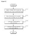
- FIG. 3 is a flow chart of a method of manufacturing a touch screen according to an embodiment of the present invention.
- the PET film 10 deposited with the ITO film 20 is heat-treated (S 110).
- the surface of the ITO film 20 is pre-processed by using the plasma or the ion beams (S120) in order to improve the adhesion of the metal layer.
- reactive gas for generating ion beams may be selected among O 2 , O 3 , N 2 , N 2 O, NO 2 , and CO 2 and may be selected among inert gases such as Ar, Kr, Xe, and Ne.
- the reactive gas or the inert gas may be applied alone or in a mixing state.
- the irradiation amount of the ion beams may be used within a range of 1 ⁇ 1015/cm 2 ⁇ 1 ⁇ 10 18 /cm 2 .
- the first metal layer, the buffer layer 40 is deposited on the pre-processed ITO film 20 (S 130).
- the buffer layer 40 may be formed by depositing a metal such as Ni, Cr, Ni-Cr, Ti, Sn, Mo, or the like by using a vacuum deposition method such as RF sputter, DC sputter, CVD technologies, or the like.
- the second metal, the conductor layer 30 is deposited on the first metal layer (S 140).
- the conductor layer 30 may be formed by depositing metals such as Ag, Cu, Au, Al, or the like using the vacuum deposition method such as RF sputter, DC sputter, CVD technologies , or the like.
- the present invention can provide the touch screen capable of providing the excellent flexibility and simplifying the manufacturing process.
Landscapes
- Engineering & Computer Science (AREA)
- Theoretical Computer Science (AREA)
- General Engineering & Computer Science (AREA)
- Human Computer Interaction (AREA)
- Physics & Mathematics (AREA)
- General Physics & Mathematics (AREA)
- Computer Hardware Design (AREA)
- Position Input By Displaying (AREA)
- Laminated Bodies (AREA)
- Physical Vapour Deposition (AREA)
- Manufacture Of Switches (AREA)
Abstract
Description
- The present invention relates to a touch screen and a method of manufacturing the same.
- A touch screen is a device detecting approached or touched positions of fingers or a touch pen. The touch screen may be mounted on a screen of a video display device to easily input information.
- The touch screen uses a transparent electrode to detect a touch input by fingers or a pen. The transparent electrode may be formed by wiring a metal layer on a transparent conductive oxide film such as indium tin oxide (ITO).
- Generally, a screen printing technology of printing and drying metal wirings has been used to form wirings on the ITO film.
- However, there is a problem in that the touch screen wiring process according to the related art is complicated. In addition, the touch screen wiring process according to the related art may make thickness of a metal layer thick. If the metal layer is thick, there are problems in that flexibility of the touch screen is weakened and the adhesion thereof is reduced.
- An embodiment of the present invention is to provide a touch screen capable of providing excellent flexibility and simplifying a manufacturing process, and a method of manufacturing the same.
- In an embodiment of the present invention, a touch screen is provided, the touch screen characterized by: a transparent conductive material deposited on a top surface of a flexible plastic film; and a metal layer vacuum-deposited on the transparent conductive film.
- In another embodiment of the present invention, a method of manufacturing a touch screen is provided, the method characterized by: performing heat treatment for preventing an ITO film from shrinking; removing and pre-processing impurities on a surface of the ITO film; and depositing a metal layer on the pre-processed ITO film.
- According to the embodiment of the present invention, the touch screen and the method of manufacturing the same capable of providing the excellent flexibility and simplifying the manufacturing process can be provided.
- The above and other objects and features of the present invention will become apparent from the following description of preferred embodiments taken in conjunction with the accompanying drawings.
-
FIG. 1 is a cross-sectional view of a touch screen according to a first embodiment of the present invention; -
FIG. 2 is a cross-sectional view of a touch screen according to a second embodiment of the present invention; and -
FIG. 3 is a flow chart of a method of manufacturing a touch screen according to an embodiment of the present invention. - Hereinafter, a touch screen and a method of manufacturing the same according to an embodiment of the present invention will be described in detail with reference to the accompanying drawings. However, if it is determined that the detailed description of relevant known functions or components makes subject matters of the present invention obscure, the detailed description thereof will be omitted.
-
FIG. 1 is a cross-sectional view of a touch screen according to a first embodiment of the present invention. - As shown in
FIG. 1 , the touch screen according to the first embodiment of the present invention includes a transparentconductive film 20 such as indium tin oxide, or the like, that is deposited on a top surface of the flexibleplastic film 10 and aconductor layer 30 that is deposited on a transparentconductive film 20. - The flexible
plastic film 10 may use a film made of PES, PC, PE, PI, Acryl, or the like, as a base. The embodiment of the present invention illustrates a case in which a polyethylene terephthalate (PET)film 10 is used, In this case, thePET film 10 has shrinkage characteristics in a range of 100 to 150°C. When thePET film 10 on which the transparentconductive film 20 is deposited is used to manufacture the touch screen, there is a problem in that an align is mismatched due to the shrinkage of thePET film 10 at the time of performing heat treatment for a bonding process of upper and lower plates. - Therefore, it is preferable to remove the shrinkage that may occur during a metal layer deposition process and a post-process by performing an annealing process that heat-treats the
PET film 10 at about 150°C for 90 minutes to shrink the film in advance. - The
conductor layer 30 is deposited on the ITOfilm 20. When the touch screen is operated in a resistive or capacitive type, the surface of the ITOfilm 20 serves to detect touch and theconductor layer 30 is used as an electrode moving charges. Therefore, theconductor layer 30 is formed using a conductive metal having a resistance value lower than that of theITO film 20. Theconductor layer 30 may be formed by depositing metals having excellent conductivity such as Ag, Cu, Au, Al, or the like using a vacuum deposition technology such as RF sputter, DC sputter, CVD , or the like. Since theconductor layer 30 directly affects the sensitivity of the touch screen, the deposition metal and the thickness may be controlled so that a resistance value may be controlled to 0.1Ω/□ (square) or less. - Meanwhile, when the
conductor layer 30 is deposited using the vacuum deposition technology, a pre-processing process of removing the impurities on the surface of theITO film 20 using plasma or ion beams may be performed in order to improve the adhesion between theITO film 20 and theconductor layer 30. -
FIG. 2 is a cross-sectional view of a touch screen according to a second embodiment of the present invention. - As shown in
FIG. 2 , the touch screen according to the second embodiment of the present invention may be used as abuffer layer 40 and aconductor layer 30 by forming the metal layer on theITO film 20 deposited on thePET film 10 in a double layer. - When the
metal layers ITO film 20 is pre-processed using a method such as plasma processing or ion beam irradiation and then, themetal layers ITO film 20 may be prevented and the adhesion and the conductivity of themetal layers - The
buffer layer 40 directly deposited on the ITOfilm 20 improves the adhesion between the ITOfilm 20 and themetal layers buffer layer 40 may use a material such as Ni, Cr, Ni-Cr, Ti, Sn, Mo, or the like and theconductor layer 30 may select a material having excellent adhesion and conductivity with thebuffer layer 40. - The
buffer layer 40 directly deposited on the ITOfilm 20 improves the adhesion between theITO film 20 and the metal layers. Therefore, thebuffer layer 40 may use a material such as Ni, Cr, Ni-Cr, Ti, Sn, Mo, or the like and theconductor layer 30 may select a material having excellent adhesion and conductivity with thebuffer layer 40. - The design conditions of the
buffer layer 40 and theconductor layer 30 and the corresponding adhesion and conductivity are as the following Table 1.[Table 1] Buffer Layer Conductor Layer Conductivity
(Surface Resistance, Ω/□)Adhesion
(kgf/cm)Experiment 1 Mo, 100 Å Ag, 800 Å 1.50 0.95 Experiment 2 Ni-Cr, 100 Å Ag, 800 Å 1.48 0.98 Experiment 3 Ni-Cr, 100 Å Cu, 1000 Å 1.10 0.97 Experiment 4 0 Ag, 1000 Å 0.88 0.3 Experiment 5 0 Cu, 1000 Å 0.94 0.34 - As listed in the above-mentioned [Table 1], the Mo/Ag
deposition ITO film 20 may be formed by depositing Mo on thebuffer layer 40 at a thickness of 100 Å and Ag on theconductor layer 30 at a thickness of 800 Å. In this case, the conductivity and the adhesion are measured as 1.50 Ω/□, 0.95 kgf/cm. - Further, the Ni-Cr/Ag
deposition ITO film 20 may be formed by depositing Ni-Cr on thebuffer layer 40 at a thickness of 100 Å and Ag on theconductor layer 30 at a thickness of 800 Å. In this case, the conductivity and the adhesion are measured as 1.48 Ω/□, 0.98 kgf/cm. - The Ni-Cr/Cu
deposition ITO film 20 may be formed by depositing Ni-Cr on thebuffer layer 40 at a thickness of 100 Å and Cu on theconductor layer 30 at a thickness of 1000 Å. In this case, the conductivity and the adhesion are measured as 1.10 Ω/□, 0.97 kgf/cm. - Further, as shown in Experiment 4 and Experiment 5, when only the
conductor layer 30 is formed, the conductivity and the adhesion are each measured as 0.88Å/□, 0.3 kgf/cm and 0.94Ω/□, 0.34 kgf/cm. - As can be appreciated from the experimental results, when the buffer layer is formed, it can be appreciated that the adhesion may be remarkably improved.
-
FIG. 3 is a flow chart of a method of manufacturing a touch screen according to an embodiment of the present invention. - As shown in
FIG. 3 , when the touch screen is manufactured according to the embodiment of the present invention, thePET film 10 deposited with theITO film 20 is heat-treated (S 110). - The surface of the
ITO film 20 is pre-processed by using the plasma or the ion beams (S120) in order to improve the adhesion of the metal layer. In this case, reactive gas for generating ion beams may be selected among O2, O3, N2, N2O, NO2, and CO2 and may be selected among inert gases such as Ar, Kr, Xe, and Ne. In addition, the reactive gas or the inert gas may be applied alone or in a mixing state. Further, the irradiation amount of the ion beams may be used within a range of 1 × 10¹⁵/cm2∼1 × 1018/cm2. - The first metal layer, the
buffer layer 40 is deposited on the pre-processed ITO film 20 (S 130). Thebuffer layer 40 may be formed by depositing a metal such as Ni, Cr, Ni-Cr, Ti, Sn, Mo, or the like by using a vacuum deposition method such as RF sputter, DC sputter, CVD technologies, or the like. - The second metal, the
conductor layer 30 is deposited on the first metal layer (S 140). Theconductor layer 30 may be formed by depositing metals such as Ag, Cu, Au, Al, or the like using the vacuum deposition method such as RF sputter, DC sputter, CVD technologies , or the like. - While the invention will be described in conjunction with exemplary embodiments, it will be understood that present description is not intended to limit the invention to those exemplary embodiments. It will be apparent to those skilled in the art that various modifications and variation can be made in the present invention without departing from the spirit or scope of the invention. Thus, it is intended that the present invention cover the modifications and variations of this invention, provided they come within the scope of the appended claims and their equivalents.
- The present invention can provide the touch screen capable of providing the excellent flexibility and simplifying the manufacturing process.
Claims (11)
- A touch screen, characterized by:a transparent conductive material deposited on a top surface of a flexible plastic film; anda metal layer vacuum-deposited on the transparent conductive film.
- The touch screen according to claim 1, characterized in that the flexible plastic film includes at least any one of PET, PES, PC, PE, PI, and Acryl.
- The touch screen according to claim 1, characterized in that the metal layer includes a conductor layer made of at least any one of Ag, Cu, Au, and Al.
- The touch screen according to claim 1, characterized in that the metal layer includes:at least any one ofNi, Cr, Ni-Cr, Ti, Sn, and Mo;a conductor layer made of at least any one of Ag, Cu, Au, and Al.
- The touch screen according to claim 1, characterized in that the metal layer is vacuum-deposited using at least any one of RF sputter, DC sputter, and CVD technologies.
- A method of manufacturing a touch screen, characterized by:performing heat treatment for preventing an ITO film from shrinking;removing and pre-processing impurities on a surface of the ITO film; and depositing a metal layer on the pre-processed ITO film
- The method according to claim 6, wherein the step of removing and pre-processing of impurities on the surface of the ITO film includes generating and pre-processing ion beams using at least any one of O2, O3, N2, N2O, NO2, and CO2.
- The method according to claim 6, wherein the step of removing and pre-processing of the impurities on the surface of the ITO film includes generating and pre-processing plasma using at least any one of Ar, Kr, Xe, and Ne.
- The method according to claim 6, wherein the step of vacuum depositing of the metal layer on the pre-processed ITO film includes forming a conductor layer by vacuum-depositing at least any one of Ag, Cu, Au, and Al.
- The method according to claim 6, wherein the step of depositing of the metal layer on the pre-processed ITO film includes:forming a buffer layer by vacuum-depositing at least any one of Ni, Cr, Ni-Cr, Ti, Sn, and Mo; andforming a conductor layer by vacuum-depositing at least any one of Ag, Cu, Au, and Al.
- The method according to claim 6, wherein the step of vacuum depositing of a metal layer on the pre-processed ITO film includes vacuum-depositing using at least any one of RF sputter, DC sputter, and CVD technologies.
Applications Claiming Priority (2)
| Application Number | Priority Date | Filing Date | Title |
|---|---|---|---|
| KR20080113678A KR101172113B1 (en) | 2008-11-14 | 2008-11-14 | Touch screen and method of manufactureing the same |
| PCT/KR2009/006668 WO2010056054A2 (en) | 2008-11-14 | 2009-11-13 | Touch screen and manufacturing method thereof |
Publications (2)
| Publication Number | Publication Date |
|---|---|
| EP2354899A2 true EP2354899A2 (en) | 2011-08-10 |
| EP2354899A4 EP2354899A4 (en) | 2013-03-27 |
Family
ID=42170527
Family Applications (1)
| Application Number | Title | Priority Date | Filing Date |
|---|---|---|---|
| EP09826286A Withdrawn EP2354899A4 (en) | 2008-11-14 | 2009-11-13 | Touch screen and manufacturing method thereof |
Country Status (6)
| Country | Link |
|---|---|
| US (1) | US8842083B2 (en) |
| EP (1) | EP2354899A4 (en) |
| JP (2) | JP2012508923A (en) |
| KR (1) | KR101172113B1 (en) |
| CN (2) | CN102216886B (en) |
| WO (1) | WO2010056054A2 (en) |
Cited By (4)
| Publication number | Priority date | Publication date | Assignee | Title |
|---|---|---|---|---|
| WO2014058116A1 (en) * | 2012-10-11 | 2014-04-17 | Lg Innotek Co., Ltd. | Touch panel and method for manufacturing the same |
| EP3035174A1 (en) * | 2014-12-16 | 2016-06-22 | Samsung Display Co., Ltd. | Touch panel and method of manufacturing the same |
| CN106168867A (en) * | 2016-07-21 | 2016-11-30 | 武汉华星光电技术有限公司 | Capacitance plate and preparation method thereof |
| KR20190045134A (en) * | 2019-04-24 | 2019-05-02 | 엘지이노텍 주식회사 | Touch panel and method for manufacturing the same |
Families Citing this family (17)
| Publication number | Priority date | Publication date | Assignee | Title |
|---|---|---|---|---|
| KR20120038194A (en) * | 2010-10-13 | 2012-04-23 | 삼성전기주식회사 | Conductive film and manufacturing method |
| JP5914036B2 (en) * | 2011-04-20 | 2016-05-11 | 日東電工株式会社 | Method for producing conductive laminated film |
| CN102184682B (en) * | 2011-04-27 | 2014-02-19 | 冠捷显示科技(厦门)有限公司 | Optical grade plastic transparent cut display and manufacturing method thereof |
| CN102314257A (en) * | 2011-09-22 | 2012-01-11 | 中兴通讯股份有限公司 | Touch device and user terminal |
| CN103252936B (en) * | 2012-02-17 | 2016-08-10 | 群康科技(深圳)有限公司 | Lamination layer structure and there is its touch control display apparatus |
| TWI482223B (en) * | 2012-11-01 | 2015-04-21 | Rtr Tech Technology Co Ltd | Method for manufacturing touch panel |
| KR20140122338A (en) * | 2013-04-09 | 2014-10-20 | 쓰리엠 이노베이티브 프로퍼티즈 캄파니 | Touch Panel, Preparing Method Thereof, and Ag-Pd-Nd Alloy for Touch Panel |
| JP2015056321A (en) * | 2013-09-12 | 2015-03-23 | 積水ナノコートテクノロジー株式会社 | Conductive film with metal layer, method for producing the same, and touch panel containing the same |
| CN103558932A (en) * | 2013-09-25 | 2014-02-05 | 昆山鑫宏达电子科技有限公司 | Cellphone touch screen |
| CN104166486A (en) * | 2014-05-09 | 2014-11-26 | 浙江金指科技有限公司 | OGS touch screen |
| KR101940693B1 (en) * | 2014-06-12 | 2019-01-22 | 주식회사 엘지화학 | Conductive structure body and method for manufacturing the same |
| CN105517335B (en) * | 2016-01-19 | 2018-11-20 | 上海万寅安全环保科技有限公司 | A kind of touch screen wiring board |
| CN105813373A (en) * | 2016-03-11 | 2016-07-27 | 上海万寅安全环保科技有限公司 | Circuit board of flexible panel |
| RU2695493C2 (en) * | 2016-05-31 | 2019-07-23 | Общество с ограниченной ответственностью "Научно-производственное предприятие Тачскрин технологии" | Projective-capacitance touch panel and method of its manufacturing |
| CN107168580A (en) * | 2017-05-16 | 2017-09-15 | 京东方科技集团股份有限公司 | A kind of Trackpad and its display screen |
| CN109785998B (en) * | 2017-11-14 | 2021-07-30 | 宁波安特弗新材料科技有限公司 | Transparent conductive film and preparation method thereof |
| CN111560586A (en) * | 2020-04-30 | 2020-08-21 | 豪威星科薄膜视窗(深圳)有限公司 | Capacitive touch screen coating process and touch screen |
Family Cites Families (29)
| Publication number | Priority date | Publication date | Assignee | Title |
|---|---|---|---|---|
| DE4239355A1 (en) * | 1992-11-24 | 1994-05-26 | Leybold Ag | Transparent substrate with a transparent layer system and method for producing such a layer system |
| JP3483355B2 (en) * | 1995-06-28 | 2004-01-06 | 三井化学株式会社 | Transparent conductive laminate |
| JPH09320761A (en) * | 1996-05-28 | 1997-12-12 | Toyota Motor Corp | EL element manufacturing method |
| JPH1064839A (en) * | 1996-08-23 | 1998-03-06 | Sony Corp | Oxide treatment method |
| JPH10112597A (en) * | 1996-10-04 | 1998-04-28 | Mitsui Petrochem Ind Ltd | Electromagnetic wave shield |
| WO2000070405A1 (en) * | 1999-05-14 | 2000-11-23 | 3M Innovative Properties Company | Ablation enhancement layer |
| JP3479023B2 (en) * | 1999-05-18 | 2003-12-15 | シャープ株式会社 | Method for manufacturing electric wiring, wiring board, display device, and image detector |
| KR100344777B1 (en) * | 2000-02-28 | 2002-07-20 | 엘지.필립스 엘시디 주식회사 | method for forming device having a thin film transistor |
| US6744425B2 (en) | 2000-12-26 | 2004-06-01 | Bridgestone Corporation | Transparent electroconductive film |
| US6896981B2 (en) * | 2001-07-24 | 2005-05-24 | Bridgestone Corporation | Transparent conductive film and touch panel |
| JP2003151366A (en) | 2001-08-02 | 2003-05-23 | Bridgestone Corp | Transparent conductive film, method for producing the same, and touch panel |
| US7151532B2 (en) | 2002-08-09 | 2006-12-19 | 3M Innovative Properties Company | Multifunctional multilayer optical film |
| JP3859569B2 (en) * | 2002-09-24 | 2006-12-20 | グンゼ株式会社 | Transparent conductive film |
| JP2005071901A (en) * | 2003-08-27 | 2005-03-17 | Teijin Dupont Films Japan Ltd | Transparent conductive laminated film |
| KR100555896B1 (en) | 2003-09-17 | 2006-03-03 | 한국과학기술연구원 | Metal Bus Electrode Manufacturing Method of Plasma Display Panel |
| JP2007272259A (en) * | 2004-04-08 | 2007-10-18 | Gunze Ltd | Transparent touch switch |
| KR101186894B1 (en) | 2004-05-07 | 2012-10-02 | 닛토덴코 가부시키가이샤 | Conductive film for touch panel and method for producing conductive film for touch panel |
| JP5299804B2 (en) | 2004-08-03 | 2013-09-25 | 綜研化学株式会社 | Adhesive sheet for attaching metal |
| US7593004B2 (en) * | 2005-06-02 | 2009-09-22 | Eastman Kodak Company | Touchscreen with conductive layer comprising carbon nanotubes |
| KR101199533B1 (en) * | 2005-06-22 | 2012-11-09 | 삼성디스플레이 주식회사 | Echant and method for fabricating interconnection line and method for fabricating thin film transistor substrate using the same |
| KR100649742B1 (en) * | 2005-10-19 | 2006-11-27 | 삼성전기주식회사 | Printed circuit board with a thin film capacitor and its manufacturing method |
| JP4754955B2 (en) * | 2005-11-07 | 2011-08-24 | 有限会社エイチエスプランニング | Conductive film for touch panel and conductive film manufacturing method for touch panel |
| WO2007069495A1 (en) * | 2005-12-16 | 2007-06-21 | Konica Minolta Medical & Graphic, Inc. | Electromagnetic wave shielding material, process for producing electromagnetic wave shielding material, and electromagnetic wave shielding material for plasma display panel |
| JP2007194109A (en) * | 2006-01-20 | 2007-08-02 | Toppan Printing Co Ltd | Conductive laminate, optical functional filter, and optical display |
| JP2008009921A (en) * | 2006-06-30 | 2008-01-17 | Optrex Corp | Input device and its manufacturing method |
| JP2008080743A (en) * | 2006-09-28 | 2008-04-10 | Optrex Corp | Touch panel device |
| JP2008140327A (en) * | 2006-12-05 | 2008-06-19 | Smk Corp | Touch panel |
| TWI451816B (en) * | 2007-03-20 | 2014-09-01 | Mitsui Mining & Smelting Co | And a resin composition for insulating layer constituting a printed circuit board |
| US20080286587A1 (en) * | 2007-05-16 | 2008-11-20 | Seagate Technology Llc | Apparatus Having Electric Circuitry and Method of Making Same |
-
2008
- 2008-11-14 KR KR20080113678A patent/KR101172113B1/en active Active
-
2009
- 2009-11-13 JP JP2011536244A patent/JP2012508923A/en active Pending
- 2009-11-13 CN CN200980145573.0A patent/CN102216886B/en active Active
- 2009-11-13 CN CN201410086522.8A patent/CN103927049B/en active Active
- 2009-11-13 EP EP09826286A patent/EP2354899A4/en not_active Withdrawn
- 2009-11-13 WO PCT/KR2009/006668 patent/WO2010056054A2/en not_active Ceased
- 2009-11-13 US US13/129,362 patent/US8842083B2/en active Active
-
2014
- 2014-03-14 JP JP2014051460A patent/JP5969527B2/en active Active
Cited By (8)
| Publication number | Priority date | Publication date | Assignee | Title |
|---|---|---|---|---|
| WO2014058116A1 (en) * | 2012-10-11 | 2014-04-17 | Lg Innotek Co., Ltd. | Touch panel and method for manufacturing the same |
| KR20140046944A (en) * | 2012-10-11 | 2014-04-21 | 엘지이노텍 주식회사 | Touch panel and method for manufacturing the same |
| US9891656B2 (en) | 2012-10-11 | 2018-02-13 | Lg Innotek Co., Ltd. | Touch panel and method for manufacturing the same |
| EP3035174A1 (en) * | 2014-12-16 | 2016-06-22 | Samsung Display Co., Ltd. | Touch panel and method of manufacturing the same |
| US9927931B2 (en) | 2014-12-16 | 2018-03-27 | Samsung Display Co., Ltd. | Touch panel and method of manufacturing the same |
| US10275105B2 (en) | 2014-12-16 | 2019-04-30 | Samsung Display Co., Ltd. | Touch panel and method of manufacturing the same |
| CN106168867A (en) * | 2016-07-21 | 2016-11-30 | 武汉华星光电技术有限公司 | Capacitance plate and preparation method thereof |
| KR20190045134A (en) * | 2019-04-24 | 2019-05-02 | 엘지이노텍 주식회사 | Touch panel and method for manufacturing the same |
Also Published As
| Publication number | Publication date |
|---|---|
| CN103927049A (en) | 2014-07-16 |
| US20110304568A1 (en) | 2011-12-15 |
| CN102216886A (en) | 2011-10-12 |
| KR101172113B1 (en) | 2012-08-10 |
| CN103927049B (en) | 2017-03-15 |
| US8842083B2 (en) | 2014-09-23 |
| JP5969527B2 (en) | 2016-08-17 |
| KR20100054674A (en) | 2010-05-25 |
| EP2354899A4 (en) | 2013-03-27 |
| WO2010056054A3 (en) | 2010-08-12 |
| CN102216886B (en) | 2015-03-11 |
| WO2010056054A2 (en) | 2010-05-20 |
| JP2014112444A (en) | 2014-06-19 |
| JP2012508923A (en) | 2012-04-12 |
Similar Documents
| Publication | Publication Date | Title |
|---|---|---|
| US8842083B2 (en) | Touch screen and manufacturing method thereof | |
| US20120038564A1 (en) | Touch Screen and Method of Manufacturing the Same | |
| US20140159285A1 (en) | Composition for laser direct structuring and laser direct structuring method using same | |
| JP5997146B2 (en) | Touch panel | |
| KR101814375B1 (en) | Transparent conductive film | |
| EP2450468A1 (en) | Method for producing transparent conductive film | |
| JP2017071850A (en) | Transparent conductive film | |
| KR101066111B1 (en) | Capacitive touch panel and manufacturing method | |
| CN103064568A (en) | Touch panel sensor | |
| CN102460352B (en) | The formation of transparent conductor film | |
| KR20120038867A (en) | Touch panel | |
| KR101942294B1 (en) | Touch screen panel and image display comprising the same | |
| KR20120086211A (en) | Method for manufacturing touch panel | |
| US9417751B2 (en) | Plate member for touch panel and method of manufacturing the same | |
| KR20120065286A (en) | Touch screen and method of manufactureing the same | |
| US20150193044A1 (en) | Touch panel and method for fabricating the touch panel | |
| US20070259190A1 (en) | ITO transparent substrate with high resistance at low-temperature sputtering process and method for producing the same | |
| KR101199047B1 (en) | Touch panel and method for manufacturing the same | |
| JP6497744B2 (en) | Touch panel | |
| KR101629665B1 (en) | Metal mesh type touch screen panel and method of manufacturing the same | |
| KR20120065285A (en) | Touch screen and method of manufactureing the same | |
| KR101385972B1 (en) | Touch panel with both elevation of view trait and printing layer | |
| JP2016157297A (en) | Transparent conductive laminate and touch panel | |
| KR20210081669A (en) | Electrode stack structure and method of fabricating the same | |
| KR101747374B1 (en) | Touch screen substrate and manufacturing method of the same |
Legal Events
| Date | Code | Title | Description |
|---|---|---|---|
| PUAI | Public reference made under article 153(3) epc to a published international application that has entered the european phase |
Free format text: ORIGINAL CODE: 0009012 |
|
| 17P | Request for examination filed |
Effective date: 20110513 |
|
| AK | Designated contracting states |
Kind code of ref document: A2 Designated state(s): AT BE BG CH CY CZ DE DK EE ES FI FR GB GR HR HU IE IS IT LI LT LU LV MC MK MT NL NO PL PT RO SE SI SK SM TR |
|
| DAX | Request for extension of the european patent (deleted) | ||
| A4 | Supplementary search report drawn up and despatched |
Effective date: 20130227 |
|
| RIC1 | Information provided on ipc code assigned before grant |
Ipc: G06F 3/045 20060101ALI20130221BHEP Ipc: G06F 3/041 20060101AFI20130221BHEP Ipc: G06F 1/16 20060101ALI20130221BHEP |
|
| 17Q | First examination report despatched |
Effective date: 20150715 |
|
| RAP1 | Party data changed (applicant data changed or rights of an application transferred) |
Owner name: LG INNOTEK CO., LTD. |
|
| STAA | Information on the status of an ep patent application or granted ep patent |
Free format text: STATUS: THE APPLICATION IS DEEMED TO BE WITHDRAWN |
|
| 18D | Application deemed to be withdrawn |
Effective date: 20191220 |