EP2339751A2 - Schaltung zum Erfassen von Kapazitätsänderungen und damit ausgestatteter Berührungsschalter - Google Patents
Schaltung zum Erfassen von Kapazitätsänderungen und damit ausgestatteter Berührungsschalter Download PDFInfo
- Publication number
- EP2339751A2 EP2339751A2 EP10196509A EP10196509A EP2339751A2 EP 2339751 A2 EP2339751 A2 EP 2339751A2 EP 10196509 A EP10196509 A EP 10196509A EP 10196509 A EP10196509 A EP 10196509A EP 2339751 A2 EP2339751 A2 EP 2339751A2
- Authority
- EP
- European Patent Office
- Prior art keywords
- capacitor
- circuit
- counter
- capacitors
- count
- Prior art date
- Legal status (The legal status is an assumption and is not a legal conclusion. Google has not performed a legal analysis and makes no representation as to the accuracy of the status listed.)
- Granted
Links
Images



Classifications
-
- G—PHYSICS
- G01—MEASURING; TESTING
- G01R—MEASURING ELECTRIC VARIABLES; MEASURING MAGNETIC VARIABLES
- G01R27/00—Arrangements for measuring resistance, reactance, impedance, or electric characteristics derived therefrom
- G01R27/02—Measuring real or complex resistance, reactance, impedance, or other two-pole characteristics derived therefrom, e.g. time constant
- G01R27/26—Measuring inductance or capacitance; Measuring quality factor, e.g. by using the resonance method; Measuring loss factor; Measuring dielectric constants ; Measuring impedance or related variables
- G01R27/2605—Measuring capacitance
-
- H—ELECTRICITY
- H03—ELECTRONIC CIRCUITRY
- H03K—PULSE TECHNIQUE
- H03K17/00—Electronic switching or gating, i.e. not by contact-making and –breaking
- H03K17/94—Electronic switching or gating, i.e. not by contact-making and –breaking characterised by the way in which the control signals are generated
- H03K17/96—Touch switches
- H03K17/962—Capacitive touch switches
- H03K17/9622—Capacitive touch switches using a plurality of detectors, e.g. keyboard
-
- G—PHYSICS
- G01—MEASURING; TESTING
- G01R—MEASURING ELECTRIC VARIABLES; MEASURING MAGNETIC VARIABLES
- G01R17/00—Measuring arrangements involving comparison with a reference value, e.g. bridge
- G01R17/02—Arrangements in which the value to be measured is automatically compared with a reference value
-
- G—PHYSICS
- G01—MEASURING; TESTING
- G01R—MEASURING ELECTRIC VARIABLES; MEASURING MAGNETIC VARIABLES
- G01R31/00—Arrangements for testing electric properties; Arrangements for locating electric faults; Arrangements for electrical testing characterised by what is being tested not provided for elsewhere
- G01R31/28—Testing of electronic circuits, e.g. by signal tracer
- G01R31/282—Testing of electronic circuits specially adapted for particular applications not provided for elsewhere
-
- G—PHYSICS
- G06—COMPUTING OR CALCULATING; COUNTING
- G06F—ELECTRIC DIGITAL DATA PROCESSING
- G06F3/00—Input arrangements for transferring data to be processed into a form capable of being handled by the computer; Output arrangements for transferring data from processing unit to output unit, e.g. interface arrangements
- G06F3/01—Input arrangements or combined input and output arrangements for interaction between user and computer
- G06F3/03—Arrangements for converting the position or the displacement of a member into a coded form
- G06F3/041—Digitisers, e.g. for touch screens or touch pads, characterised by the transducing means
- G06F3/044—Digitisers, e.g. for touch screens or touch pads, characterised by the transducing means by capacitive means
-
- H—ELECTRICITY
- H03—ELECTRONIC CIRCUITRY
- H03K—PULSE TECHNIQUE
- H03K2217/00—Indexing scheme related to electronic switching or gating, i.e. not by contact-making or -breaking covered by H03K17/00
- H03K2217/94—Indexing scheme related to electronic switching or gating, i.e. not by contact-making or -breaking covered by H03K17/00 characterised by the way in which the control signal is generated
- H03K2217/96—Touch switches
- H03K2217/9607—Capacitive touch switches
- H03K2217/960705—Safety of capacitive touch and proximity switches, e.g. increasing reliability, fail-safe
-
- H—ELECTRICITY
- H03—ELECTRONIC CIRCUITRY
- H03K—PULSE TECHNIQUE
- H03K2217/00—Indexing scheme related to electronic switching or gating, i.e. not by contact-making or -breaking covered by H03K17/00
- H03K2217/94—Indexing scheme related to electronic switching or gating, i.e. not by contact-making or -breaking covered by H03K17/00 characterised by the way in which the control signal is generated
- H03K2217/96—Touch switches
- H03K2217/9607—Capacitive touch switches
- H03K2217/96071—Capacitive touch switches characterised by the detection principle
- H03K2217/960715—Rc-timing; e.g. measurement of variation of charge time or discharge time of the sensor
-
- H—ELECTRICITY
- H03—ELECTRONIC CIRCUITRY
- H03K—PULSE TECHNIQUE
- H03K2217/00—Indexing scheme related to electronic switching or gating, i.e. not by contact-making or -breaking covered by H03K17/00
- H03K2217/94—Indexing scheme related to electronic switching or gating, i.e. not by contact-making or -breaking covered by H03K17/00 characterised by the way in which the control signal is generated
- H03K2217/96—Touch switches
- H03K2217/9607—Capacitive touch switches
- H03K2217/960735—Capacitive touch switches characterised by circuit details
- H03K2217/960745—Capacitive differential; e.g. comparison with reference capacitance
Definitions
- Some preferred embodiments of the present invention relate to a capacitance discrimination circuit configured to discriminate capacitance added to a terminal, a touch switch equipped with the capacitance discrimination circuit, and a capacitance discrimination method.
- an input device for various electronics devices such as, e.g., a mobile phone, a mobile audio device, a handheld gaming gadget, a television, or a personal computer
- a touch switch or a touch sensor equipped with electrode switches hereinafter simply referred to as "touch switch” in this document
- this kind of input device is disclosed by Japanese Unexamined Laid-open Patent Application Publication No. 2000-65514 ( JP-A-2000-65514 ).
- Such a conventional touch switch configured to detect capacitance changes, it is discriminated whether or not the touch switch, more specifically an electrode switch provided on a touch panel, is being touched by a finger of a user by measuring a voltage of a capacitor attached to a terminal (electrode switch).
- Fig. 5 is an explanatory view of an operation of a touch switch.
- This touch switch has two electrode switches 1a and 1b on a touch panel P, and is configured to discriminate whether or not the electrode switch is being touched by a finger F of a user.
- the capacitance C2' of the finger F is added to the capacitance C2 of the electrode switch 1b.
- the electrode switch 1b becomes larger in capacitance.
- Fig. 6 shows voltage increase changes of two capacitors C1 and C2 different in capacitance. As shown in this figure, these capacitors C1 and C2 are different in voltage increase rate, causing a difference in time required for each capacitor to reach a reference voltage Vref, which enables discrimination of a difference of capacitance in these capacitors C1 and C2. At this time, provided that the capacitor C1 and the capacitor C2 are designed to have the same capacitance, since the apparent capacitance of the capacitor C2 is larger than that of the capacitor C1, it can be discriminated that the electrode switch having the larger apparent capacitance C2 is being touched by a finger of a user. This principle can be utilized in a touch switch.
- external noises may cause a slower voltage increase rate of the electrode switch even if the switch is not being touched by a finger of a user.
- the conventional touch switch may sometimes recognize that the slower voltage increase rate was caused by a touch of a user's finger to the electrode switch, and may erroneously discriminate that the touch switch is being touched by a finger of a user.
- Fig. 7 is a graph showing voltage changes of a capacitor in which the solid line shows a voltage change in cases where the capacitor is not affected by noise and the dashed-line shows a voltage change in cases where the capacitor is affected by noise.
- the voltage increases smoothly.
- the capacitor is affected by noise, as shown in the dashed line, even if electric charges are added gradually, the voltage does not increase smoothly, resulting in unsteady voltage increase, which causes erroneous discrimination.
- the preferred embodiments of the present invention have been developed in view of the above-mentioned and/or other problems in the related art.
- the preferred embodiments of the present invention can significantly improve upon existing methods and/or apparatuses.
- some embodiments can provide a capacitance discrimination circuit capable of assuredly discriminating capacitance changes while minimizing external noise influence.
- some embodiments can provide a touch panel equipped with the capacitance discrimination circuit.
- some embodiments can provide a capacitance discrimination method capable of assuredly discriminating capacitance changes while minimizing external noise influence.
- some embodiments can provide a capacitance discrimination circuit including a first capacitor, a second capacitor, a comparator configured to compare a first voltage of the first capacitor and a second voltage of the second capacitor, a counter circuit configured to perform a count operation based on a comparison result of the comparator, a charge circuit configured to charge the first capacitor and the second capacitor, and a control circuit configured to control the charge circuit so as to charge either the first capacitor or the second capacitor based on a comparison result of the comparator.
- the capacitance discrimination of the first capacitor and the second capacitor is performed based on count values of the counter circuit.
- the counter circuit includes a first counter configured to perform a count operation when the comparison result of the comparator is a first value, a second counter configured to perform a count operation when the comparison result of the comparator is not the first value, and a third counter configured to count a predetermined time period.
- the capacitance discrimination of the first capacitor and the second capacitor is performed based on the count values of the first counter and the second counter.
- the capacitance discrimination circuit further includes a discharge circuit configured to discharge electric charges stored in the first capacitor and the second capacitor.
- This discharge circuit causes discharging of the electric charges stored in the first capacitor and the second capacitor in accordance with a discharge signal from the control circuit.
- some preferred embodiments provide a touch switch equipped with the aforementioned capacitance discrimination circuit.
- the touch switch is configured to discriminate whether or not a finger of a user is being touched based on the discrimination result of the capacitance discrimination circuit.
- some preferred embodiments provide a capacitance discrimination method of discriminating capacitance of a plurality of capacitors.
- the method includes the steps of comparing voltages of the plurality of capacitors, performing a count operation on one of the plurality of capacitors lowest in voltage based on a comparison result of the voltages of the plurality of capacitors to obtain a count value on each of the plurality of capacitors, charging one of the plurality of capacitors lowest in voltage based on the comparison result of the voltages of the plurality of capacitors, and discriminating capacitance of the plurality of capacitors based on the count values of the count operation.
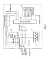
- FIG. 1 shows a block diagram of a capacitance discrimination circuit.
- a touch panel has a first electrode (terminal) 1a and a second electrode (terminal) 1b provided thereon.
- One end of the first electrode 1a is connected by one end of a first capacitor C1 with the other end of the capacitor grounded, and similarly one end of the second electrode 1b is connected by one end of a second capacitor C2 with the other end of the capacitor grounded.
- These electrodes 1a and 1b are connected to first and second terminals 2a and 2b of an LSI circuit at their other ends, respectively, so that the voltages of the first and second capacitors C1 and C2 are applied to the LSI circuit.
- the LSI circuit includes a comparator 3 having a non-inverting terminal and an inverting terminal to which signals from the capacitors C1 and C2 are input respectively. With this structure, voltages of the capacitors C1 and C2 can be compared. The comparison result is output to a control circuit 4.
- the control circuit 4 samples the comparison result upon receipt of a clock signal. When it is discriminated by the sampling result that the voltage of the first capacitor C1 is lower than that of the second capacitor C2, a counter circuit 5 causes a count-up operation of a first counter 5a.
- the counter circuit 5 when it is discriminated by the sampling result that the voltage of the first capacitor C1 is higher than that of the second capacitor C2 (i.e., the voltage of the second capacitor C2 is lower than that of the first capacitor C1), the counter circuit 5 causes a count-up operation of a second counter 5a.
- the counter circuit 5 has a third counter 5c which measures a prescribed time period.
- the third counter 5c starts the counting operation upon receipt of a start signal from the control circuit 4, and sends a termination flag signal to the control circuit 4 when the counter overflows.
- the control circuit 4 receives this termination flag signal to recognize that the prescribed time period has passed, and compares the count values of the first counter 5a and the second counter 5b.
- the control circuit 4 outputs a charge signal, a first switch signal, and a second switch signal.
- a charge signal Upon receipt of a charge signal, the capacitor C30 and the capacitor C40 in the charge circuit 6 are charged by a certain amount of electric charges.
- the capacitors C30 and C40 can be provided outside of the LSI circuit, since these capacitors C30 and C40 are merely required to store a small amount of electric charges, it is preferable to have such capacitors C30 and C40 built-in the LSI circuit, which can reduce the production cost by eliminating the number of external parts.
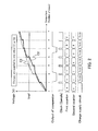
- Fig. 2 is a timing chart of the aforementioned operation. Comparing the voltages of the capacitors C1 and C2, no charge is supplied to the capacitor higher in voltage, while a certain amount of charge is supplied to the capacitor lower in voltage. More specifically, in the initial comparison, since the voltage of the capacitor C2 is lower than that of the capacitor C1, the second counter 5b counts up, and electric charges are supplied only to the capacitor C2. In the second comparison, the voltage of the capacitor C1 becomes lower than that of the capacitor C2, and therefore the first counter 5a counts up, and electric charges are supplied only to the capacitor C1.
- a conventional touch switch can be affected by noises entered via the terminal as discussed previously.
- the voltage comparison between the electrodes of the touch switch since the voltage comparison between the electrodes of the touch switch is performed, an influence by common noises entered in both electrodes can be ignored. Furthermore, no high-performance A/D and/or D/A converter is required, which becomes possible to perform high accuracy capacitance discrimination with relatively simple structure. Provided that electric charges remain in the capacitors C1 and C2, electric charges are initially kept supplied only to one of capacitors C1 and C2 lower in voltage. However, the other capacitor becomes lower in voltage in due course.
- the aforementioned method causes a waste of time until the voltage inversion of the capacitors C1 and C2 occurs, which requires a longer time for the discrimination. Shortening of the discrimination time can be attained by adding a discharge circuit 7 as shown in Fig. 1 .
- the control circuit 4 outputs a discharge signal to the discharge circuit 7.
- the discharge circuit 7 receives the discharge signal, the transistors SW3 and SW4 in the discharge circuit 7 go into an on-state, which causes discharging of both the capacitors C1 and C2.
- Fig. 3 is a timing chart showing the case in which capacitors C1 and C2 are discharged in accordance with the discharge signal.
- the voltages of the electrodes 1a and 1b become equal in accordance with the input of the discharge signal.
- sampling of the outputs of the comparator 3 is performed in synchronization with a clock input, and only the capacitor connected to the electrode lower in voltage is charged using the first switch signal or the second switch signal.
- the capacitance of the touch switch is discriminated by detecting the voltage increase.
- the capacitance discrimination can also be performed by detecting the voltage decrease.
- such capacitor discrimination can be performed by supplying sufficient electric charges to the capacitors C1 and C2, then comparing the voltages, and lowering the higher voltage by discharging a certain amount of electric charges.
- the number of electrodes is not limited to the above, and can be increased, such as, e.g., 3, 4, 5, 6, ..., or N.
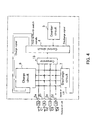
- Fig. 4 is a block diagram showing a capacitance discrimination circuit according to a second embodiment. Cumulative explanation on the same portions as the first embodiment shown in Fig. 1 will be omitted.
- electrodes 1c and 1d are added and the total number of electrodes is 4 (four).
- the comparator 13 is configured to extract the lowest voltage among the voltages of the first to fourth electrodes 1a, 1b, 1c, and 1d. The output of the comparator 13 is supplied to the control circuit 4.
- the counter circuit 5 is equipped with a plurality of counters each configured to perform the count operation when the corresponding capacitor becomes the lowest voltage among the voltages of the capacitors C1 to C4. Comparing the count values of the counters enables discrimination of the capacitance of each capacitor. Even if the number of electrodes becomes N, the same capacitance discrimination can be performed.
- the first counter 5a configured to operate the count-up operation when the capacitor C1 is lower in voltage than the capacitor C2
- the second counter 5b configured to operate the count-up operation when the capacitor C2 is lower in voltage than capacitor C1 are provided separately.
- an up/down counter which is configured to perform a count-up operation when the capacitor C1 is lower in voltage than the capacitor C2 and a count-down operation when the capacitor C2 is lower in voltage than the capacitor C1
- the aforementioned explanation is made while referring to the case in which the capacitors C1 and C2 of the electrodes 1a and 1b are the same in capacitance.
- the present invention can be applied to the case in which the capacitors of the electrodes are different in capacitance from each other.
- the aforementioned explanation is made while referring to the case in which the capacitors C30 and C40 in the charge circuit 6 are the same in capacitance.
- the present invention can be applied to the case in which the capacitors C30 and C40 are different in capacitance. In cases where the capacitor C1 is smaller in capacitance than the capacitor C2 (C1 ⁇ C2), since the voltage of the capacitor C1 quickly rises.
- the capacitance discrimination can be performed by judging the count value of the counter circuit 5.
- the capacitance of the capacitor C30 is twice as large as that of the capacitor C40, the electric charge of the capacitor C40 becomes equal to that of the capacitor C30 when the capacitor C40 is charged twice. Therefore, the amount of electric charges supplied to the capacitor C1 from the capacitor C30 becomes twice as large as the amount of electric charges supplied to the capacitor C2 from the capacitor C40.
- the capacitance discrimination can be performed by judging the count value.
- the term "preferably” is non-exclusive and means “preferably, but not limited to.”
- means-plus-function or step-plus-function limitations will only be employed where for a specific claim limitation all of the following conditions are present in that limitation: a) "means for” or “step for” is expressly recited; b) a corresponding function is expressly recited; and c) structure, material or acts that support that structure are not recited.
- the terminology "present invention” or “invention” is meant as a non-specific, general reference and may be used as a reference to one or more aspect within the present disclosure.
Landscapes
- Physics & Mathematics (AREA)
- General Physics & Mathematics (AREA)
- Engineering & Computer Science (AREA)
- General Engineering & Computer Science (AREA)
- Electronic Switches (AREA)
- Position Input By Displaying (AREA)
- Geophysics And Detection Of Objects (AREA)
Applications Claiming Priority (1)
| Application Number | Priority Date | Filing Date | Title |
|---|---|---|---|
| JP2009290567A JP2011133964A (ja) | 2009-12-22 | 2009-12-22 | 容量判別回路、容量判別回路を備えたタッチスイッチ |
Publications (3)
| Publication Number | Publication Date |
|---|---|
| EP2339751A2 true EP2339751A2 (de) | 2011-06-29 |
| EP2339751A3 EP2339751A3 (de) | 2012-11-07 |
| EP2339751B1 EP2339751B1 (de) | 2014-01-15 |
Family
ID=43755226
Family Applications (1)
| Application Number | Title | Priority Date | Filing Date |
|---|---|---|---|
| EP10196509.3A Not-in-force EP2339751B1 (de) | 2009-12-22 | 2010-12-22 | Schaltung zum Erfassen von Kapazitätsänderungen und damit ausgestatteter Berührungsschalter |
Country Status (4)
| Country | Link |
|---|---|
| US (1) | US8552747B2 (de) |
| EP (1) | EP2339751B1 (de) |
| JP (1) | JP2011133964A (de) |
| KR (1) | KR101216813B1 (de) |
Cited By (2)
| Publication number | Priority date | Publication date | Assignee | Title |
|---|---|---|---|---|
| WO2013075344A1 (zh) * | 2011-11-23 | 2013-05-30 | 江苏惠通集团有限责任公司 | 触摸识别方法及装置、空间鼠标及其控制方法 |
| DE102012006546A1 (de) * | 2012-04-02 | 2013-10-02 | Trw Automotive Electronics & Components Gmbh | Kapazitiver Sensor, Verfahren zum Auslesen eines kapazitiven Sensorfeldes und Verfahren zur Herstellung eines kapazitiven Sensorfeldes |
Families Citing this family (6)
| Publication number | Priority date | Publication date | Assignee | Title |
|---|---|---|---|---|
| US8599169B2 (en) * | 2011-12-14 | 2013-12-03 | Freescale Semiconductor, Inc. | Touch sense interface circuit |
| KR101431884B1 (ko) * | 2011-12-21 | 2014-08-27 | 삼성전기주식회사 | 터치 스크린 패널 |
| TWI477747B (zh) * | 2012-05-08 | 2015-03-21 | Egalax Empia Technology Inc | 抑制低頻雜訊干擾的感測方法與裝置 |
| FR2999833B1 (fr) * | 2012-12-19 | 2015-01-23 | Continental Automotive France | Dispositif de mesure d'une variation d'une capacite et procede de mesure associe |
| CN111669165B (zh) * | 2020-07-08 | 2024-11-15 | 童宗伟 | 一种非触点压力开关控制方法和装置 |
| CN119550995B (zh) * | 2024-12-06 | 2025-10-21 | 上海科世达-华阳汽车电器有限公司 | 一种方向盘的离手检测方法、系统、控制器及装置 |
Citations (2)
| Publication number | Priority date | Publication date | Assignee | Title |
|---|---|---|---|---|
| JP2000065514A (ja) | 1998-08-20 | 2000-03-03 | Nippon Telegr & Teleph Corp <Ntt> | 表面形状認識用センサ回路 |
| JP2009290567A (ja) | 2008-05-29 | 2009-12-10 | Canon Inc | データ送信装置及びデータ受信装置 |
Family Cites Families (11)
| Publication number | Priority date | Publication date | Assignee | Title |
|---|---|---|---|---|
| JPS59171219A (ja) * | 1983-03-17 | 1984-09-27 | Nec Corp | レベル検出回路 |
| US6897673B2 (en) * | 2003-03-19 | 2005-05-24 | Lsi Logic Corporation | Method and integrated circuit for capacitor measurement with digital readout |
| JP4310695B2 (ja) * | 2004-03-30 | 2009-08-12 | アイシン精機株式会社 | 静電容量変化検出装置 |
| JP4363281B2 (ja) * | 2004-09-08 | 2009-11-11 | オムロン株式会社 | 容量計測装置および方法、並びにプログラム |
| WO2007075887A2 (en) * | 2005-12-21 | 2007-07-05 | Weiss Instruments, Inc. | Micropower voltage-independent capacitance measuring method and circuit |
| CN1832349A (zh) * | 2006-04-19 | 2006-09-13 | 北京希格玛晶华微电子有限公司 | 一种电容测量触摸感应、辨认方法及实现装置 |
| JP2009042903A (ja) * | 2007-08-07 | 2009-02-26 | Seiko Instruments Inc | 表示装置付静電検出装置及び静電容量検出方法 |
| US20090045823A1 (en) * | 2007-08-13 | 2009-02-19 | Winbond Electronics Corporation | Power efficient capacitive detection |
| JP5104150B2 (ja) * | 2007-09-14 | 2012-12-19 | オムロン株式会社 | 検知装置および方法、並びにプログラム |
| JP2009193139A (ja) * | 2008-02-12 | 2009-08-27 | Seiko Instruments Inc | 近接検出装置及びその方法 |
| JP5191769B2 (ja) * | 2008-03-27 | 2013-05-08 | ルネサスエレクトロニクス株式会社 | 容量検出装置及び方法 |
-
2009
- 2009-12-22 JP JP2009290567A patent/JP2011133964A/ja not_active Ceased
-
2010
- 2010-12-21 KR KR1020100131499A patent/KR101216813B1/ko not_active Expired - Fee Related
- 2010-12-22 US US12/976,182 patent/US8552747B2/en active Active
- 2010-12-22 EP EP10196509.3A patent/EP2339751B1/de not_active Not-in-force
Patent Citations (2)
| Publication number | Priority date | Publication date | Assignee | Title |
|---|---|---|---|---|
| JP2000065514A (ja) | 1998-08-20 | 2000-03-03 | Nippon Telegr & Teleph Corp <Ntt> | 表面形状認識用センサ回路 |
| JP2009290567A (ja) | 2008-05-29 | 2009-12-10 | Canon Inc | データ送信装置及びデータ受信装置 |
Cited By (4)
| Publication number | Priority date | Publication date | Assignee | Title |
|---|---|---|---|---|
| WO2013075344A1 (zh) * | 2011-11-23 | 2013-05-30 | 江苏惠通集团有限责任公司 | 触摸识别方法及装置、空间鼠标及其控制方法 |
| DE102012006546A1 (de) * | 2012-04-02 | 2013-10-02 | Trw Automotive Electronics & Components Gmbh | Kapazitiver Sensor, Verfahren zum Auslesen eines kapazitiven Sensorfeldes und Verfahren zur Herstellung eines kapazitiven Sensorfeldes |
| DE102012006546B4 (de) * | 2012-04-02 | 2018-02-08 | Trw Automotive Electronics & Components Gmbh | Kapazitiver Sensor, Verfahren zum Auslesen eines kapazitiven Sensorfeldes und Verfahren zur Herstellung eines kapazitiven Sensorfeldes |
| US10018661B2 (en) | 2012-04-02 | 2018-07-10 | Trw Automotive Electronics & Components Gmbh | Capacitive sensor, method for reading out a capacitive sensor field and method for producing a capacitive sensor field |
Also Published As
| Publication number | Publication date |
|---|---|
| KR101216813B1 (ko) | 2012-12-28 |
| US20110148439A1 (en) | 2011-06-23 |
| US8552747B2 (en) | 2013-10-08 |
| KR20110073333A (ko) | 2011-06-29 |
| EP2339751A3 (de) | 2012-11-07 |
| JP2011133964A (ja) | 2011-07-07 |
| EP2339751B1 (de) | 2014-01-15 |
Similar Documents
| Publication | Publication Date | Title |
|---|---|---|
| US8552747B2 (en) | Capacitance discrimination circuit and touch switch equipped with the same | |
| CN101833044B (zh) | 用于确定电容值的系统和方法 | |
| US8125232B2 (en) | Capacitive sensing device and method | |
| US8134374B2 (en) | Evaluation circuit for capacitance and method thereof | |
| US10514403B2 (en) | Capacitance measuring circuit and capacitance measuring method | |
| JP4310695B2 (ja) | 静電容量変化検出装置 | |
| JP4888743B2 (ja) | 静電容量検出装置 | |
| US20170131838A1 (en) | Touch control apparatus and noise compensating circuit and method thereof | |
| JP2013506905A (ja) | 静電容量式タッチセンサデバイス設定システムおよび方法 | |
| US20090225044A1 (en) | Determining touch on keys of touch sensitive input device | |
| CN102163109B (zh) | 触控感测系统、电容感测装置及电容感测方法 | |
| US10684726B2 (en) | Capacitive touch sensing circuit and charge compensation method thereof | |
| EP3971694B1 (de) | Geräuschdetektionsschaltung, eigenkapazitätsdetektionsverfahren, berührungs-chip und elektronische vorrichtung | |
| EP4270790A1 (de) | Kapazitive sensorvorrichtung mit driftkompensation | |
| US9660645B2 (en) | Door handle module for vehicle and apparatus for locking and unlocking vehicle door including the module | |
| US10733468B2 (en) | Finger stability detecting method and fingerprint sensing device | |
| US9841855B2 (en) | Systems and methods for capacitive touch detection | |
| US10754469B2 (en) | Touch detection method and touch detection apparatus | |
| US20130181947A1 (en) | Touch screen panel | |
| EP3490148B1 (de) | Kapazitätsdetektionsvorrichtung | |
| CN114924128A (zh) | 电容检测电路、集成电路、电子设备以及电容检测方法 | |
| US11243237B2 (en) | Method for determining an electrical parameter and measurement arrangement for determining an electrical parameter | |
| KR101085403B1 (ko) | 근접 터치를 센싱하는 방법 및 그 장치 | |
| KR101507138B1 (ko) | 터치 인식시스템 및 터치 인식방법 | |
| WO2015131329A1 (en) | Method and apparatus for capacitive sensing |
Legal Events
| Date | Code | Title | Description |
|---|---|---|---|
| PUAI | Public reference made under article 153(3) epc to a published international application that has entered the european phase |
Free format text: ORIGINAL CODE: 0009012 |
|
| AK | Designated contracting states |
Kind code of ref document: A2 Designated state(s): AL AT BE BG CH CY CZ DE DK EE ES FI FR GB GR HR HU IE IS IT LI LT LU LV MC MK MT NL NO PL PT RO RS SE SI SK SM TR |
|
| AX | Request for extension of the european patent |
Extension state: BA ME |
|
| PUAL | Search report despatched |
Free format text: ORIGINAL CODE: 0009013 |
|
| AK | Designated contracting states |
Kind code of ref document: A3 Designated state(s): AL AT BE BG CH CY CZ DE DK EE ES FI FR GB GR HR HU IE IS IT LI LT LU LV MC MK MT NL NO PL PT RO RS SE SI SK SM TR |
|
| AX | Request for extension of the european patent |
Extension state: BA ME |
|
| RIC1 | Information provided on ipc code assigned before grant |
Ipc: H03K 17/96 20060101AFI20120928BHEP |
|
| 17P | Request for examination filed |
Effective date: 20130507 |
|
| RBV | Designated contracting states (corrected) |
Designated state(s): AL AT BE BG CH CY CZ DE DK EE ES FI FR GB GR HR HU IE IS IT LI LT LU LV MC MK MT NL NO PL PT RO RS SE SI SK SM TR |
|
| GRAP | Despatch of communication of intention to grant a patent |
Free format text: ORIGINAL CODE: EPIDOSNIGR1 |
|
| INTG | Intention to grant announced |
Effective date: 20130726 |
|
| GRAS | Grant fee paid |
Free format text: ORIGINAL CODE: EPIDOSNIGR3 |
|
| GRAA | (expected) grant |
Free format text: ORIGINAL CODE: 0009210 |
|
| AK | Designated contracting states |
Kind code of ref document: B1 Designated state(s): AL AT BE BG CH CY CZ DE DK EE ES FI FR GB GR HR HU IE IS IT LI LT LU LV MC MK MT NL NO PL PT RO RS SE SI SK SM TR |
|
| REG | Reference to a national code |
Ref country code: GB Ref legal event code: FG4D Ref country code: CH Ref legal event code: EP |
|
| REG | Reference to a national code |
Ref country code: AT Ref legal event code: REF Ref document number: 650203 Country of ref document: AT Kind code of ref document: T Effective date: 20140215 |
|
| REG | Reference to a national code |
Ref country code: IE Ref legal event code: FG4D |
|
| REG | Reference to a national code |
Ref country code: DE Ref legal event code: R096 Ref document number: 602010013115 Country of ref document: DE Effective date: 20140227 |
|
| REG | Reference to a national code |
Ref country code: NL Ref legal event code: VDEP Effective date: 20140115 |
|
| REG | Reference to a national code |
Ref country code: AT Ref legal event code: MK05 Ref document number: 650203 Country of ref document: AT Kind code of ref document: T Effective date: 20140115 |
|
| REG | Reference to a national code |
Ref country code: LT Ref legal event code: MG4D |
|
| PG25 | Lapsed in a contracting state [announced via postgrant information from national office to epo] |
Ref country code: LT Free format text: LAPSE BECAUSE OF FAILURE TO SUBMIT A TRANSLATION OF THE DESCRIPTION OR TO PAY THE FEE WITHIN THE PRESCRIBED TIME-LIMIT Effective date: 20140115 Ref country code: IS Free format text: LAPSE BECAUSE OF FAILURE TO SUBMIT A TRANSLATION OF THE DESCRIPTION OR TO PAY THE FEE WITHIN THE PRESCRIBED TIME-LIMIT Effective date: 20140515 Ref country code: NO Free format text: LAPSE BECAUSE OF FAILURE TO SUBMIT A TRANSLATION OF THE DESCRIPTION OR TO PAY THE FEE WITHIN THE PRESCRIBED TIME-LIMIT Effective date: 20140415 |
|
| PG25 | Lapsed in a contracting state [announced via postgrant information from national office to epo] |
Ref country code: NL Free format text: LAPSE BECAUSE OF FAILURE TO SUBMIT A TRANSLATION OF THE DESCRIPTION OR TO PAY THE FEE WITHIN THE PRESCRIBED TIME-LIMIT Effective date: 20140115 Ref country code: CY Free format text: LAPSE BECAUSE OF FAILURE TO SUBMIT A TRANSLATION OF THE DESCRIPTION OR TO PAY THE FEE WITHIN THE PRESCRIBED TIME-LIMIT Effective date: 20140115 Ref country code: AT Free format text: LAPSE BECAUSE OF FAILURE TO SUBMIT A TRANSLATION OF THE DESCRIPTION OR TO PAY THE FEE WITHIN THE PRESCRIBED TIME-LIMIT Effective date: 20140115 Ref country code: FI Free format text: LAPSE BECAUSE OF FAILURE TO SUBMIT A TRANSLATION OF THE DESCRIPTION OR TO PAY THE FEE WITHIN THE PRESCRIBED TIME-LIMIT Effective date: 20140115 Ref country code: SE Free format text: LAPSE BECAUSE OF FAILURE TO SUBMIT A TRANSLATION OF THE DESCRIPTION OR TO PAY THE FEE WITHIN THE PRESCRIBED TIME-LIMIT Effective date: 20140115 Ref country code: ES Free format text: LAPSE BECAUSE OF FAILURE TO SUBMIT A TRANSLATION OF THE DESCRIPTION OR TO PAY THE FEE WITHIN THE PRESCRIBED TIME-LIMIT Effective date: 20140115 Ref country code: PT Free format text: LAPSE BECAUSE OF FAILURE TO SUBMIT A TRANSLATION OF THE DESCRIPTION OR TO PAY THE FEE WITHIN THE PRESCRIBED TIME-LIMIT Effective date: 20140515 |
|
| PG25 | Lapsed in a contracting state [announced via postgrant information from national office to epo] |
Ref country code: LV Free format text: LAPSE BECAUSE OF FAILURE TO SUBMIT A TRANSLATION OF THE DESCRIPTION OR TO PAY THE FEE WITHIN THE PRESCRIBED TIME-LIMIT Effective date: 20140115 Ref country code: HR Free format text: LAPSE BECAUSE OF FAILURE TO SUBMIT A TRANSLATION OF THE DESCRIPTION OR TO PAY THE FEE WITHIN THE PRESCRIBED TIME-LIMIT Effective date: 20140115 Ref country code: BE Free format text: LAPSE BECAUSE OF FAILURE TO SUBMIT A TRANSLATION OF THE DESCRIPTION OR TO PAY THE FEE WITHIN THE PRESCRIBED TIME-LIMIT Effective date: 20140115 Ref country code: RS Free format text: LAPSE BECAUSE OF FAILURE TO SUBMIT A TRANSLATION OF THE DESCRIPTION OR TO PAY THE FEE WITHIN THE PRESCRIBED TIME-LIMIT Effective date: 20140115 |
|
| REG | Reference to a national code |
Ref country code: DE Ref legal event code: R097 Ref document number: 602010013115 Country of ref document: DE |
|
| PG25 | Lapsed in a contracting state [announced via postgrant information from national office to epo] |
Ref country code: RO Free format text: LAPSE BECAUSE OF FAILURE TO SUBMIT A TRANSLATION OF THE DESCRIPTION OR TO PAY THE FEE WITHIN THE PRESCRIBED TIME-LIMIT Effective date: 20140115 Ref country code: DK Free format text: LAPSE BECAUSE OF FAILURE TO SUBMIT A TRANSLATION OF THE DESCRIPTION OR TO PAY THE FEE WITHIN THE PRESCRIBED TIME-LIMIT Effective date: 20140115 Ref country code: EE Free format text: LAPSE BECAUSE OF FAILURE TO SUBMIT A TRANSLATION OF THE DESCRIPTION OR TO PAY THE FEE WITHIN THE PRESCRIBED TIME-LIMIT Effective date: 20140115 Ref country code: CZ Free format text: LAPSE BECAUSE OF FAILURE TO SUBMIT A TRANSLATION OF THE DESCRIPTION OR TO PAY THE FEE WITHIN THE PRESCRIBED TIME-LIMIT Effective date: 20140115 |
|
| PLBE | No opposition filed within time limit |
Free format text: ORIGINAL CODE: 0009261 |
|
| STAA | Information on the status of an ep patent application or granted ep patent |
Free format text: STATUS: NO OPPOSITION FILED WITHIN TIME LIMIT |
|
| PG25 | Lapsed in a contracting state [announced via postgrant information from national office to epo] |
Ref country code: PL Free format text: LAPSE BECAUSE OF FAILURE TO SUBMIT A TRANSLATION OF THE DESCRIPTION OR TO PAY THE FEE WITHIN THE PRESCRIBED TIME-LIMIT Effective date: 20140115 Ref country code: SK Free format text: LAPSE BECAUSE OF FAILURE TO SUBMIT A TRANSLATION OF THE DESCRIPTION OR TO PAY THE FEE WITHIN THE PRESCRIBED TIME-LIMIT Effective date: 20140115 |
|
| 26N | No opposition filed |
Effective date: 20141016 |
|
| REG | Reference to a national code |
Ref country code: DE Ref legal event code: R097 Ref document number: 602010013115 Country of ref document: DE Effective date: 20141016 |
|
| PG25 | Lapsed in a contracting state [announced via postgrant information from national office to epo] |
Ref country code: SI Free format text: LAPSE BECAUSE OF FAILURE TO SUBMIT A TRANSLATION OF THE DESCRIPTION OR TO PAY THE FEE WITHIN THE PRESCRIBED TIME-LIMIT Effective date: 20140115 |
|
| REG | Reference to a national code |
Ref country code: DE Ref legal event code: R119 Ref document number: 602010013115 Country of ref document: DE |
|
| PG25 | Lapsed in a contracting state [announced via postgrant information from national office to epo] |
Ref country code: LU Free format text: LAPSE BECAUSE OF FAILURE TO SUBMIT A TRANSLATION OF THE DESCRIPTION OR TO PAY THE FEE WITHIN THE PRESCRIBED TIME-LIMIT Effective date: 20141222 |
|
| REG | Reference to a national code |
Ref country code: CH Ref legal event code: PL |
|
| GBPC | Gb: european patent ceased through non-payment of renewal fee |
Effective date: 20141222 |
|
| REG | Reference to a national code |
Ref country code: IE Ref legal event code: MM4A |
|
| REG | Reference to a national code |
Ref country code: FR Ref legal event code: ST Effective date: 20150831 |
|
| PG25 | Lapsed in a contracting state [announced via postgrant information from national office to epo] |
Ref country code: CH Free format text: LAPSE BECAUSE OF NON-PAYMENT OF DUE FEES Effective date: 20141231 Ref country code: LI Free format text: LAPSE BECAUSE OF NON-PAYMENT OF DUE FEES Effective date: 20141231 Ref country code: DE Free format text: LAPSE BECAUSE OF NON-PAYMENT OF DUE FEES Effective date: 20150701 Ref country code: GB Free format text: LAPSE BECAUSE OF NON-PAYMENT OF DUE FEES Effective date: 20141222 Ref country code: IE Free format text: LAPSE BECAUSE OF NON-PAYMENT OF DUE FEES Effective date: 20141222 |
|
| PG25 | Lapsed in a contracting state [announced via postgrant information from national office to epo] |
Ref country code: FR Free format text: LAPSE BECAUSE OF NON-PAYMENT OF DUE FEES Effective date: 20141231 |
|
| PG25 | Lapsed in a contracting state [announced via postgrant information from national office to epo] |
Ref country code: SM Free format text: LAPSE BECAUSE OF FAILURE TO SUBMIT A TRANSLATION OF THE DESCRIPTION OR TO PAY THE FEE WITHIN THE PRESCRIBED TIME-LIMIT Effective date: 20140115 |
|
| PG25 | Lapsed in a contracting state [announced via postgrant information from national office to epo] |
Ref country code: MC Free format text: LAPSE BECAUSE OF FAILURE TO SUBMIT A TRANSLATION OF THE DESCRIPTION OR TO PAY THE FEE WITHIN THE PRESCRIBED TIME-LIMIT Effective date: 20140115 |
|
| PG25 | Lapsed in a contracting state [announced via postgrant information from national office to epo] |
Ref country code: IT Free format text: LAPSE BECAUSE OF FAILURE TO SUBMIT A TRANSLATION OF THE DESCRIPTION OR TO PAY THE FEE WITHIN THE PRESCRIBED TIME-LIMIT Effective date: 20140115 Ref country code: GR Free format text: LAPSE BECAUSE OF FAILURE TO SUBMIT A TRANSLATION OF THE DESCRIPTION OR TO PAY THE FEE WITHIN THE PRESCRIBED TIME-LIMIT Effective date: 20140416 Ref country code: BG Free format text: LAPSE BECAUSE OF FAILURE TO SUBMIT A TRANSLATION OF THE DESCRIPTION OR TO PAY THE FEE WITHIN THE PRESCRIBED TIME-LIMIT Effective date: 20140115 |
|
| PG25 | Lapsed in a contracting state [announced via postgrant information from national office to epo] |
Ref country code: TR Free format text: LAPSE BECAUSE OF FAILURE TO SUBMIT A TRANSLATION OF THE DESCRIPTION OR TO PAY THE FEE WITHIN THE PRESCRIBED TIME-LIMIT Effective date: 20140115 Ref country code: HU Free format text: LAPSE BECAUSE OF FAILURE TO SUBMIT A TRANSLATION OF THE DESCRIPTION OR TO PAY THE FEE WITHIN THE PRESCRIBED TIME-LIMIT; INVALID AB INITIO Effective date: 20101222 Ref country code: MT Free format text: LAPSE BECAUSE OF FAILURE TO SUBMIT A TRANSLATION OF THE DESCRIPTION OR TO PAY THE FEE WITHIN THE PRESCRIBED TIME-LIMIT Effective date: 20140115 |
|
| PG25 | Lapsed in a contracting state [announced via postgrant information from national office to epo] |
Ref country code: MK Free format text: LAPSE BECAUSE OF FAILURE TO SUBMIT A TRANSLATION OF THE DESCRIPTION OR TO PAY THE FEE WITHIN THE PRESCRIBED TIME-LIMIT Effective date: 20140115 |
|
| PG25 | Lapsed in a contracting state [announced via postgrant information from national office to epo] |
Ref country code: AL Free format text: LAPSE BECAUSE OF FAILURE TO SUBMIT A TRANSLATION OF THE DESCRIPTION OR TO PAY THE FEE WITHIN THE PRESCRIBED TIME-LIMIT Effective date: 20140115 |