EP2338320B1 - Schutzabdeckung für eine flexible leiterplatte - Google Patents
Schutzabdeckung für eine flexible leiterplatte Download PDFInfo
- Publication number
- EP2338320B1 EP2338320B1 EP09765003.0A EP09765003A EP2338320B1 EP 2338320 B1 EP2338320 B1 EP 2338320B1 EP 09765003 A EP09765003 A EP 09765003A EP 2338320 B1 EP2338320 B1 EP 2338320B1
- Authority
- EP
- European Patent Office
- Prior art keywords
- protective cover
- circuit board
- printed circuit
- flexible printed
- protective
- Prior art date
- Legal status (The legal status is an assumption and is not a legal conclusion. Google has not performed a legal analysis and makes no representation as to the accuracy of the status listed.)
- Active
Links
Images
Classifications
-
- H—ELECTRICITY
- H05—ELECTRIC TECHNIQUES NOT OTHERWISE PROVIDED FOR
- H05K—PRINTED CIRCUITS; CASINGS OR CONSTRUCTIONAL DETAILS OF ELECTRIC APPARATUS; MANUFACTURE OF ASSEMBLAGES OF ELECTRICAL COMPONENTS
- H05K3/00—Apparatus or processes for manufacturing printed circuits
-
- H—ELECTRICITY
- H05—ELECTRIC TECHNIQUES NOT OTHERWISE PROVIDED FOR
- H05K—PRINTED CIRCUITS; CASINGS OR CONSTRUCTIONAL DETAILS OF ELECTRIC APPARATUS; MANUFACTURE OF ASSEMBLAGES OF ELECTRICAL COMPONENTS
- H05K1/00—Printed circuits
- H05K1/02—Details
- H05K1/11—Printed elements for providing electric connections to or between printed circuits
- H05K1/118—Printed elements for providing electric connections to or between printed circuits specially for flexible printed circuits, e.g. using folded portions
-
- H—ELECTRICITY
- H05—ELECTRIC TECHNIQUES NOT OTHERWISE PROVIDED FOR
- H05K—PRINTED CIRCUITS; CASINGS OR CONSTRUCTIONAL DETAILS OF ELECTRIC APPARATUS; MANUFACTURE OF ASSEMBLAGES OF ELECTRICAL COMPONENTS
- H05K2201/00—Indexing scheme relating to printed circuits covered by H05K1/00
- H05K2201/10—Details of components or other objects attached to or integrated in a printed circuit board
- H05K2201/10227—Other objects, e.g. metallic pieces
- H05K2201/10393—Clamping a component by an element or a set of elements
-
- H—ELECTRICITY
- H05—ELECTRIC TECHNIQUES NOT OTHERWISE PROVIDED FOR
- H05K—PRINTED CIRCUITS; CASINGS OR CONSTRUCTIONAL DETAILS OF ELECTRIC APPARATUS; MANUFACTURE OF ASSEMBLAGES OF ELECTRICAL COMPONENTS
- H05K2201/00—Indexing scheme relating to printed circuits covered by H05K1/00
- H05K2201/20—Details of printed circuits not provided for in H05K2201/01 - H05K2201/10
- H05K2201/2009—Reinforced areas, e.g. for a specific part of a flexible printed circuit
-
- H—ELECTRICITY
- H05—ELECTRIC TECHNIQUES NOT OTHERWISE PROVIDED FOR
- H05K—PRINTED CIRCUITS; CASINGS OR CONSTRUCTIONAL DETAILS OF ELECTRIC APPARATUS; MANUFACTURE OF ASSEMBLAGES OF ELECTRICAL COMPONENTS
- H05K2203/00—Indexing scheme relating to apparatus or processes for manufacturing printed circuits covered by H05K3/00
- H05K2203/01—Tools for processing; Objects used during processing
- H05K2203/0147—Carriers and holders
- H05K2203/0165—Holder for holding a Printed Circuit Board [PCB] during processing, e.g. during screen printing
-
- H—ELECTRICITY
- H05—ELECTRIC TECHNIQUES NOT OTHERWISE PROVIDED FOR
- H05K—PRINTED CIRCUITS; CASINGS OR CONSTRUCTIONAL DETAILS OF ELECTRIC APPARATUS; MANUFACTURE OF ASSEMBLAGES OF ELECTRICAL COMPONENTS
- H05K2203/00—Indexing scheme relating to apparatus or processes for manufacturing printed circuits covered by H05K3/00
- H05K2203/01—Tools for processing; Objects used during processing
- H05K2203/0147—Carriers and holders
- H05K2203/0169—Using a temporary frame during processing
-
- H—ELECTRICITY
- H05—ELECTRIC TECHNIQUES NOT OTHERWISE PROVIDED FOR
- H05K—PRINTED CIRCUITS; CASINGS OR CONSTRUCTIONAL DETAILS OF ELECTRIC APPARATUS; MANUFACTURE OF ASSEMBLAGES OF ELECTRICAL COMPONENTS
- H05K3/00—Apparatus or processes for manufacturing printed circuits
- H05K3/0058—Laminating printed circuit boards onto other substrates, e.g. metallic substrates
Definitions
- the invention relates to a protective cover for the protective support of a flexible printed circuit board. Furthermore, the invention relates to a printed circuit board with such a protective cover.
- Flexible circuit boards have a flexible film of insulating material with firmly adhering conductive connections and serve for a mechanical fastening and electrical connection of electronic components. On surfaces of the flexible printed circuit boards contact surfaces are mounted, with a perfect condition of the contact surfaces for subsequent error-free use of the flexible printed circuit board is a prerequisite.
- a process chain for the production, further processing and assembly of a flexible printed circuit board comprises a plurality of individual process steps, which are linked together by different handling and / or transport steps.
- by manual and / or mechanical handling and / or transport steps may damage the contact surface by scratching and contamination of the contact surface by hand sweat, oil or grease and particles present on a support surface occur.
- Such damaged or contaminated flexible printed circuit boards are not suitable for further use.
- the US 2003/0089784 A1 discloses a card-like device having a rigid circuit board, a conductive frame for supporting the circuit board, and a conductive cover disposed on the conductive frame surrounding the circuit board in communication with the conductive frame.
- the frame is further provided with engagement portions adjacent to the corresponding ones first contact areas are formed in the frame area.
- Each engagement portion includes a rib that protrudes along the inner peripheral wall of the frame portion and defines the board receiving area.
- Each rib extends parallel to the surfaces of the board receiving area, and is located opposite the projection at the end of each arm. Between the projection and the rib, a gap is formed, in which the circuit board can be inserted.
- the DE 94 19 187 U1 describes a flat card case for check cards, phone cards and smart cards, whose receiving space for one of the cards below bounded by a bottom part, which merges into two guide strips at the SolCodesrändem, and top of an upper side is, wherein a front-side insertion opening for insertion of a card is provided in the receiving space, and wherein the bottom part has at least one extending in the longitudinal direction housing recess, which is arranged in an area in which the magnetic strip is inserted card.
- the US 1,288,395 describes a business card protective cover, wherein the business card can be inserted through an opening at one end of the shell.
- the US 4,450,955 describes a protective cover for card-shaped data carrier with a protective unit and a receiving unit, wherein the protective unit is designed frame-shaped, and wherein the protective unit has a rectangular base plate with two oppositely arranged removal openings.
- a protective cover wherein a protective unit of the protective cover covers the surface in a protective manner and a receiving unit serves to securely receive the flexible printed circuit board in the protective cover.
- a protective cover is inexpensive.
- a protective cover according to claim 2 can be easily removed from a flexible circuit board.
- a protective cover according to claim 3 guarantees a secure recording of a flexible circuit board.
- a protective cover according to claim 4 guarantees a secure mounting of a flexible printed circuit board in the protective cover.
- a protective cover according to claim 5 is inexpensive to produce.
- a protective cover according to claim 6 allows a defined and secure storage of a flexible circuit board.
- a protective cover according to claim 7 serves for a secure receiving a flexible printed circuit board.
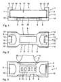
- FIGS. 1 to 3 illustrated first embodiment of a protective cover 1 comprises a protective unit 2 and a receiving unit 3.
- the protection unit 2 is formed like a frame and has a centrally disposed, rectangular protective opening 4.
- the protective opening 4 may also assume other basic forms, in particular the protective opening 4 may be round, elliptical, hexagonal or octagonal.
- the protective unit 2 is integrally connected to the receiving unit 3, wherein the protective cover 1 made of a material that allows a reshaping production of the protective cover 1, in particular plastic or metal.
- the protective cover 1 has a storage surface 5 for safe storage of the protective cover 1 on a flat surface.
- the protection unit 2 has a rectangular base plate 6 with two oppositely arranged, trapezoidal recesses 7 and two oppositely arranged Ent.öfnitch 8.
- the recesses 7 and the removal openings 8 are each arranged at opposite edges 9, 10 of the base plate 6.
- the receiving unit 3 has two side walls 11 and four side guides 12.
- the two side walls 11 are arranged on two opposite edges 10 of the base plate 6 such that the side walls 11 project vertically from the base plate 6.
- a locking projection 13 is provided for latching receiving a flexible printed circuit board 14, wherein the locking projection 13 has an insertion slope 15 and a removal bevel 16 for insertion and removal of the flexible printed circuit board 14.
- the side guides 12 are arranged perpendicularly projecting from the base plate 6, wherein the side guides 12 are arranged on the outer edges 9 of the base plate 6, that a lateral guidance of a male flexible printed circuit board 14 is made possible.
- the two latching projections 13 define an insertion opening 18 located therebetween.
- the flexible printed circuit board 14 has a stiffening plate 19 and a carrier film 20 with a surface 21 to be protected, in particular a contact surface. In a latching recording of the flexible printed circuit board 14 in the protective cover 1, the surface 21 is arranged on the protective opening 4 such that accessibility of the surface 21 is.
- the in the FIGS. 1 to 3 shown protective cover 1 is used for secure recording by a latching holder of the flexible circuit board 14.
- the flexible circuit board 14 is inserted from one of the storage surface 5 opposite side of the protective cover 1 in the receiving space 17.
- the flexible circuit board 14 is connected to the stiffening plate 19th placed on the locking projections 13, wherein the side walls 11 are pressed laterally outwards by a pressure on the stiffening plate 19 in the direction of the receiving space 17, so that the insertion opening 18 is increased until the flexible printed circuit board 14 via the insertion bevels 15 through the insertion opening 18th enters the receiving space 17.
- the flexible printed circuit board 14 is arranged during the latching recording in the protective cover 1 such that the carrier film 20 rests on the base plate 6 and all edges of the stiffening plate 19 are partially enclosed by the receiving unit 3.
- the connection of the flexible printed circuit board 14 with the protective cover 1 is detachable.
- the flexible printed circuit board 14 is pushed away from the protective unit 2 upwards out of the receiving space 17.
- pressure is exerted on the carrier film 20 of the flexible printed circuit board 14, so that the latching projections 13 are pressed laterally outwards analogously to the insertion process, so that the flexible printed circuit board 14 can be removed via the removal slants 16 through the insertion opening 18 from the receiving space 17.
- the pressure on the carrier film 20 is applied through the removal openings 8 or to the recesses 7.
- a protective cover 1, which is detachably connectable to a flexible printed circuit board 14, can be detached from the flexible printed circuit board 14 at the end of a process chain and subsequently reused.
- a protective cover 1 can be used for receiving a plurality of different types of flexible printed circuit boards 14. It is also possible, the protective cover 1 at the end of a process chain with the flexible circuit board 14 to leave connected and to integrate the protective cover 1 in a subsequent assembly of the flexible printed circuit board 14 in an electronic module and in particular to use as part of a housing of the electronic module.
Landscapes
- Engineering & Computer Science (AREA)
- Manufacturing & Machinery (AREA)
- Microelectronics & Electronic Packaging (AREA)
- Structure Of Printed Boards (AREA)
- Non-Metallic Protective Coatings For Printed Circuits (AREA)
- Casings For Electric Apparatus (AREA)
Description
- Die Erfindung betrifft eine Schutzabdeckung zur schützenden Halterung einer flexiblen Leiterplatte. Ferner betrifft die Erfindung eine Leiterplatte mit einer derartigen Schutzabdeckung.
- Flexible Leiterplatten weisen eine flexible Folie aus isolierendem Material mit fest haftenden leitenden Verbindungen auf und dienen einer mechanischen Befestigung und elektrischen Verbindung elektronischer Bauteile. An Oberflächen der flexiblen Leiterplatten sind Kontaktflächen angebracht, wobei ein einwandfreier Zustand der Kontaktflächen für eine nachfolgende fehlerfreie Verwendung der flexiblen Leiterplatte Voraussetzung ist.
- Eine Prozesskette zur Herstellung, Weiterverarbeitung und Montage einer flexiblen Leiterplatte umfasst eine Vielzahl an einzelnen Prozessschritten, die durch verschiedene Handhabungs- und/oder Transportschritte miteinander verknüpft sind. Insbesondere durch manuelle und/oder maschinelle Handhabungs- und/oder Transportschritte können Beschädigungen der Kontaktfläche durch Verkratzen und Verunreinigung der Kontaktfläche durch Handschweiß, Öl bzw. Fett und vorhandenen Partikeln auf einer Auflagefläche auftreten. Derartig beschädigte oder verunreinigte flexible Leiterplatten sind für eine weitere Verwendung nicht geeignet.
- Zum Schutz von Kontaktflächen vor Beeinträchtigungen durch Verunreinigung oder Beschädigung werden Schutzauflcleber, die auf die Kontaktflächen aufgeklebt werden, vorgesehen. Bei einer Entfernung des Schutzaufklebers können Rückstände einer Klebeschicht auf der Kontaktfläche verbleiben, sodass eine Verunreinigung der Kontaktfläche resultiert. Weiterhin sind separate Schutzeinrichtungen zur Verwendung in einzelnen Fertigungsanlagen sowie aufwendige Handhabungsschritte in Form einer manuellen Handhabung mit Schutzhandschuhen oder zusätzlichen, aufwändig gestalteten Greifer-Systemen bei einer maschinellen Handhabung bekannt. Die genannten Schutzvorkehrungen sind anlagen- und/oder zeitaufwändig und deshalb kostenintensiv. Weiterhin besteht die Gefahr von Beschädigung und/oder Verunreinigung der Kontaktflächen nach Beendigung eines Prozessschrittes und anschließender Handhabung oder Transport der flexiblen Leiterplatten.
- Die
US 2003/0089784 A1 beschreit eine kartenähnliche Vorrichtung mit einer starren Leiterplatte, einen leitenden Rahmen zum Unterstützen der Leiterplatte, und eine leitende Verkleidung, angeordnet am leitenden Rahmen, die in Verbindung mit dem leitendem Rahmen die Leiterplatte umgibt.Der Rahmen weiterhin ausgestattet mit Eingriffbereichen, welche benachbart zu den entsprechenden ersten Kontaktbereichen im Rahmenbereich angeformt sind. Jeder Eingriffbereich umfasst eine Rippe , die entlang der inneren Umfangswand des Rahmenbereichs hervortritt und den Leiterplattenaufnahmebereich definiert. Jede Rippe erstreckt sich parallel zu den Oberflächen des Leiterplattenaufnahmebereiches, und ist gegenüber dem Vorsprung am Ende jeden Armes angeordnet. Zwischen dem Vorsprung und der Rippe ist eine Lücke ausgebildet, in die die Leiterplatte eingeführt werden kann. - Die
DE 94 19 187 U1 beschreibt eine flache Kartenhülle für Scheckkarten, Telefonkarten und Chipkarten, deren Aufnahmeraum für eine der genannten Karten unten von einem Bodenteil, das an den Seitenlängsrändem in zwei Führungsstreifen übergeht, und oben von einer Oberseite begrenzt ist, wobei eine stirnseitige Einschuböffnung zum Einschieben einer Karte in den Aufnahmeraum vorgesehen ist, und wobei das Bodenteil mindestens eine in Hüllenlängsrichtung verlaufende Vertiefung aufweist, die in einem Bereich angeordnet ist, in dem sich bei eingeschobener Karte der Magnetstreifen befindet. - Die
US 1,288,395 beschreibt eine Visitenkartenschutzhülle, wobei die Visitenkarte durch eine Öffnung an einem Ende der Hülle eingeschoben werden kann. - Die
US 4,450,955 beschreibt eine Schutzabdeckung für kartenförmige Datenträger mit einer Schutzeinheit und einer Aufnahmeeinheit, wobei die Schutzeinheit rahmenförmig ausgebildet ist, und wobei die Schutzeinheit eine rechteckige Grundplatte mit zwei gegenüberliegend angeordneten Entnahmeöffnungen aufweist. - All diesen Dokumenten ist gemein, dass der zu schützende Gegenstand in die Schutzabdeckung eingeführt bzw. eingeschoben wird, was die Gefahr birgt, dass dabei dessen Oberfläche beschädigt wird.
- Es ist die Aufgabe der vorliegenden Erfindung, eine Schutzabdeckung zur schützenden Halterung einer flexiblen Leiterplatte derart zu schaffen, dass eine Oberfläche der flexiblen Leiterplatte entlang einer gesamten Prozesskette von einer Herstellung bis zu einer Montage der flexiblen Leiterplatte kostengünstig und zuverlässig vor Beschädigung und/oder Verunreinigung geschützt ist.
- Diese Aufgabe ist erfindungsgemäß durch eine Schutzabdeckung mit den im Anspruch 1 angegebenen Merkmalen gelöst.
- Erfindungsgemäß wurde erkannt, dass ein umfassender Schutz einer Oberfläche einer flexiblen Leiterplatte durch eine Schutzabdeckung erfolgt, wobei eine Schutz-Einheit der Schutzabdeckung die Oberfläche schützend abdeckt und eine Aufnahme-Einheit einer sicheren Aufnahme der flexiblen Leiterplatte in der Schutzabdeckung dient. Eine derartige Schutzabdeckung ist kostengünstig.
- Eine Schutzabdeckung nach Anspruch 2 kann von einer flexiblen Leiterplatte einfach entfernt werden.
- Eine Schutzabdeckung nach Anspruch 3 garantiert eine sichere Aufnahme einer flexiblen Leiterplatte.
- Eine Schutzabdeckung nach Anspruch 4 garantiert eine sichere Halterung einer flexiblen Leiterplatte in der Schutzabdeckung.
- Eine Schutzabdeckung nach Anspruch 5 ist kostengünstig herstellbar.
- Eine Schutzabdeckung nach Anspruch 6 ermöglicht eine definierte und sichere Ablage einer flexiblen Leiterplatte.
- Eine Schutzabdeckung nach Anspruch 7 dient einer sicheren Aufnahme einer flexiblen Leiterplatte.
- Die Vorteile einer Leiterplatte nach Anspruch 8 entsprechen denen der unter den vorgenannten Ansprüchen erläuterten Vorteilen. Ausführungsbeispiele der Erfindung werden nachfolgend anhand der Zeichnung näher erläutert. In dieser zeigen:
- Fig. 1
- eine Seitenansicht eines ersten Ausführungsbeispiels einer Schutzabdeckung mit Rastvorsprüngen und einer rastend aufgenommenen flexiblen Leiterplatte;
- Fig. 2
- eine Draufsicht der in
Figur 1 dargestellten Schutzabdeckung ohne Darstellung der flexiblen Leiterplatte; - Fig. 3
- eine Ansicht von unten der in
Figur 1 dargestellten Schutzabdeckung mit flexibler Leiterplatte; - Ein in den
Figuren 1 bis 3 dargestelltes erstes Ausführungsbeispiel einer Schutzabdeckung 1 umfasst eine Schutz-Einheit 2 und eine Aufnahme-Einheit 3. Die Schutzeinheit 2 ist rahmenförmig ausgebildet und weist eine zentral angeordnete, rechteckige Schutzöffnung 4 auf. Die Schutzöffnung 4 kann auch andere Grundformen annehmen, insbesondere kann die Schutzöffnung 4 rund, ellipsenförmig, sechseckig oder achteckig sein. Die Schutz-Einheit 2 ist mit der Aufnahme-Einheit 3 einstückig verbunden, wobei die Schutzabdeckung 1 aus einem Material, das eine umformende Herstellung der Schutzabdeckung 1 erlaubt, insbesondere Kunststoff oder Metall, besteht. Weiterhin weist die Schutzabdeckung 1 eine Ablagefläche 5 zur sicheren Ablage der Schutzabdeckung 1 auf einer ebenen Unterlage auf. Die Schutz-Einheit 2 weist eine rechteckige Grundplatte 6 mit zwei gegenüberliegend angeordneten, trapezförmigen Ausnehmungen 7 sowie zwei gegenüberliegend angeordnete Entnahmeöfnungen 8 auf. Die Ausnehmungen 7 und die Entnahmeöffnungen 8 sind jeweils an gegenüberliegenden Kanten 9, 10 der Grundplatte 6 angeordnet. Die Aufnahme-Einheit 3 weist zwei Seitenwände 11 und vier Seitenführungen 12 auf. Die beiden Seitenwände 11 sind an zwei gegenüberliegenden Kanten 10 der Grundplatte 6 derart angeordnet, dass die Seitenwände 11 senkrecht von der Grundplatte 6 hervorstehen. An einem mit der Grundfläche 6 verbundenen Ende gegenüberliegenden Ende der Seitenwand 11 ist ein Rastvorsprung 13 zur rastenden Aufnahme einer flexiblen Leiterplatte 14 vorgesehen, wobei der Rastvorsprung 13 eine Einfuhrschräge 15 und eine Entnahmeschräge 16 zum Einführen und Entnehmen der flexiblen Leiterplatte 14 aufweist. Die Seitenführungen 12 sind senkrecht von der Grundplatte 6 abstehend angeordnet, wobei die Seitenführungen 12 derart an den Außenkanten 9 der Grundplatte 6 angeordnet sind, dass eine seitliche Führung einer aufzunehmenden flexiblen Leiterplatte 14 ermöglicht wird. Von den Seitenführungen 12, den Seitenwänden 11, der Grundplatte 6 und den Rastvorsprüngen 13 wird ein Aufnahme-Raum 17 umgrenzt, der für die Aufnahme der flexiblen Leiterplatte 14 vorgesehen ist. Die beiden Rastvorsprünge 13 begrenzen eine dazwischen liegende Einführöffnung 18. Die flexible Leiterplatte 14 weist eine Aussteifungsplatte 19 und eine Trägerfolie 20 mit einer zu schützenden Oberfläche 21, insbesondere einer Kontaktfläche, auf. Bei einer rastenden Aufnahme der flexiblen Leiterplatte 14 in der Schutzabdeckung 1 ist die Oberfläche 21 an der Schutzöffnung 4 derart angeordnet, dass eine Zugänglichkeit der Oberfläche 21 besteht. - Die in den
Figuren 1 bis 3 dargestellte Schutzabdeckung 1 dient der sicheren Aufnahme durch eine rastende Halterung der flexiblen Leiterplatte 14. Dazu wird die flexible Leiterplatte 14 von einer der Ablagefläche 5 gegenüberliegenden Seite der Schutzabdeckung 1 in den Aufnahme-Raum 17 eingeführt. Die flexible Leiterplatte 14 wird mit der Aussteifungsplatte 19 auf den Rastvorsprüngen 13 abgelegt, wobei durch einen Druck auf die Aussteifungsplatte 19 in Richtung des Aufnahme-Raumes 17 die Seitenwände 11 seitlich nach außen gedrückt werden, sodass die Einführöffnung 18 vergrößert wird, bis die flexible Leiterplatte 14 über die Einführschrägen 15 durch die Einführöffnung 18 in den Aufnahme-Raum 17 gelangt. Die flexible Leiterplatte 14 ist während der rastenden Aufnahme in der Schutzabdeckung 1 derart angeordnet, dass die Trägerfolie 20 auf der Grundplatte 6 aufliegt und alle Kanten der Aussteifungsplatte 19 von der Aufnahme-Einheit 3 abschnittsweise umschlossen werden. Die Verbindung der flexiblen Leiterplatte 14 mit der Schutzabdeckung 1 ist lösbar. Zum Lösen der flexiblen Leiterplatte 14 aus der Schutzabdeckung 1 wird die flexible Leiterplatte 14 von der Schutzeinheit 2 weg nach oben aus dem Aufnahme-Raum 17 herausgedrückt. Dazu wird Druck auf die Trägerfolie 20 der flexiblen Leiterplatte 14 ausgeübt, sodass die Rastvorsprünge 13 analog dem Einführvorgang seitlich nach außen gedrückt werden, sodass die flexible Leiterplatte 14 über die Entnahmeschrägen 16 durch die Einführöffnung 18 aus dem Aufnahmeraum 17 entnehmbar ist. Um eine Beschädigung und/oder Verschmutzung der Oberfläche 21 der Trägerfolie 20 während der Entnahme zu vermeiden, wird der Druck auf die Trägerfolie 20 durch die Entnahmeöffnungen 8 oder an den Ausnehmungen 7 aufgebracht. - Eine Schutzabdeckung 1, die lösbar mit einer flexiblen Leiterplatte 14 verbindbar ist, kann am Ende einer Prozesskette von der flexiblen Leiterplatte 14 gelöst und anschließend wieder verwendet werden. Bei einer geeigneten Gestaltung einer Aufnahme-Einheit 3 und einer Schutzeinheit 2kann eine Schutzabdeckung 1 für die Aufnahme mehrerer, verschiedenartiger flexibler Leiterplatten 14 verwendet werden. Es ist weiterhin möglich, die Schutzabdeckung 1 am Ende einer Prozesskette mit der flexiblen Leiterplatte 14 verbunden zu lassen und die Schutzabdeckung 1 bei einer anschließenden Montage der flexiblen Leiterplatte 14 in eine elektronische Baugruppe zu integrieren und insbesondere als Teil eines Gehäuses der elektronischen Baugruppe zu verwenden.
Claims (8)
- Schutzabdeckung (1) zur schützenden Halterung einer flexiblen Leiterplatte (14), mit einer Trägerfolie (20) und einer Aussteifungsplatte (19),umfassend- eine Schutz-Einheit (2) zur Abdeckung einer Oberfläche (21) der flexiblen Leiterplatte (14) und- eine Aufnahme-Einheit (3) zur sicheren Aufnahme einer Aussteifungsplatte (19) der flexiblen Leiterplatte (14) mit der Schutzabdeckung (1), wobei die Schutz-Einheit (2) rahmenförmig ausgebildet ist, so dass die zu schützende Oberfläche (21) der flexiblen Leiterplatte (14) zugänglich ist, dadurch gekennzeichnet, dass,- die Aufnahme-Einheit (3) aus mehreren Seitenwänden (11, 12) mit Rastvorsprüngen (13) zur rastenden Aufnahme der Aussteifungsplatte (19) gebildet wird, wobei die Rastvorsprünge (13) Einführschrägen (15) und Entnahmeschrägen (16) zum Einführen und Entnehmen der Aussteifungsplatte (19) aufweisen, und- die Schutz-Einheit (2) eine rechteckige Grundplatte (6) mit zwei gegenüberliegend angeordneten, trapezförmigen Ausnehmungen (7) sowie zwei gegenüberliegend angeordnete Entnahmeöffnungen (8) aufweist, wobei die Ausnehmungen (7) und die Entnahmeöffnungen (8) geeignet sind, Druck auf die Trägerfolie (20) zum Lösen der flexiblen Leiterplatte (14) aus der Schutzabdeckung (1) derart aufzubringen, dass die flexible Leiterplatte (14) von der Schutzeinheit (2) weg nach oben herausgedrückt werden kann.
- Schutzabdeckung (1) nach einem der vorgenannten Ansprüche, dadurch gekennzeichnet, dass die Aussteifungsplatte (19) lösbar mit der Schutzabdeckung (1) verbunden ist.
- Schutzabdeckung (1) nach einem der vorgenannten Ansprüche, dadurch gekennzeichnet, dass die Aufnahme-Einheit (3) alle Kanten der Aussteifungsplatte (19) abschnittsweise umschließt.
- Schutzabdeckung (1) nach Anspruch 1, dadurch gekennzeichnet, dass die flexible Leiterplatte (14) unlösbar, insbesondere durch eine formschlüssige Steck-Verbindung, verbunden ist.
- Schutzabdeckung (1) nach einem der vorgenannten Ansprüche, dadurch gekennzeichnet, dass die Schutzabdeckung (1) aus Kunststoff besteht.
- Schutzabdeckung (1) nach einem der vorgenannten Ansprüche, dadurch gekennzeichnet, dass die Schutzabdeckung (1) eine Ablagefläche (5) zur sicheren Ablage auf einer ebenen Unterlage aufweist.
- Schutzabdeckung (1) nach einem der vorgenannten Ansprüche, dadurch gekennzeichnet, dass die Schutzabdeckung (1) einstückig hergestellt ist.
- Leiterplatte (14) mit einer Schutzabdeckung (1) nach einem der vorgenannten Ansprüche, wobei die Leiterplatte (14) von der Schutzabdeckung (1) aufgenommen ist.
Applications Claiming Priority (2)
| Application Number | Priority Date | Filing Date | Title |
|---|---|---|---|
| DE102008052243A DE102008052243A1 (de) | 2008-10-18 | 2008-10-18 | Schutzabdeckung für eine flexible Leiterplatte |
| PCT/DE2009/001410 WO2010043204A1 (de) | 2008-10-18 | 2009-10-09 | Schutzabdeckung für eine flexible leiterplatte |
Publications (2)
| Publication Number | Publication Date |
|---|---|
| EP2338320A1 EP2338320A1 (de) | 2011-06-29 |
| EP2338320B1 true EP2338320B1 (de) | 2013-04-17 |
Family
ID=41571162
Family Applications (1)
| Application Number | Title | Priority Date | Filing Date |
|---|---|---|---|
| EP09765003.0A Active EP2338320B1 (de) | 2008-10-18 | 2009-10-09 | Schutzabdeckung für eine flexible leiterplatte |
Country Status (5)
| Country | Link |
|---|---|
| US (1) | US8785783B2 (de) |
| EP (1) | EP2338320B1 (de) |
| JP (1) | JP5548862B2 (de) |
| DE (2) | DE102008052243A1 (de) |
| WO (1) | WO2010043204A1 (de) |
Families Citing this family (5)
| Publication number | Priority date | Publication date | Assignee | Title |
|---|---|---|---|---|
| DE102008052244A1 (de) * | 2008-10-18 | 2010-04-22 | Carl Freudenberg Kg | Flexible Leiterplatte |
| SE538701C2 (en) * | 2014-12-19 | 2016-10-25 | Autoliv Dev | Electrical unit |
| DE102015216419B4 (de) * | 2015-08-27 | 2022-06-15 | Vitesco Technologies GmbH | Elektronisches Gerät mit einem Gehäuse mit einer darin angeordneten Leiterplatte |
| CN112089519B (zh) * | 2019-12-31 | 2022-07-19 | 未来穿戴技术有限公司 | 眼部按摩仪 |
| DE102024120758A1 (de) * | 2024-07-22 | 2026-01-22 | Valeo Detection Systems GmbH | Optische Erfassungseinheit mit spezifischer Anordnung einer flexiblen Leiterplatte und eines elektrischen Steckers in einem Gehäuse sowie Verfahren |
Family Cites Families (29)
| Publication number | Priority date | Publication date | Assignee | Title |
|---|---|---|---|---|
| US1288395A (en) | 1917-02-02 | 1918-12-17 | Addressograph Co | Combined printing and identification device. |
| US4450955A (en) | 1981-12-04 | 1984-05-29 | Featherston Elmer F | Card holder |
| JPS61124421A (ja) * | 1984-11-20 | 1986-06-12 | Matsushita Electric Ind Co Ltd | パレツト装置 |
| JPS61154094A (ja) * | 1984-12-26 | 1986-07-12 | 住友ベークライト株式会社 | フレキシブルプリント回路板の製造方法 |
| JPH0230869Y2 (de) * | 1985-02-28 | 1990-08-20 | ||
| DE69000924T2 (de) | 1989-04-28 | 1993-06-03 | Nikken Ind Corp | Leiterplatte und ueberzug. |
| JPH0644200U (ja) * | 1992-11-19 | 1994-06-10 | 住友ベークライト株式会社 | 基板固定治具 |
| DE9307959U1 (de) | 1993-05-26 | 1993-08-05 | Ritter, Gerhard, 74076 Heilbronn | Kartenhülle für Chipkarten |
| JPH08511674A (ja) * | 1993-06-09 | 1996-12-03 | ユナイテッド テクノロジーズ オートモーティブ,インコーポレイテッド | ハイブリッドジャンクションボックス |
| DE59307515D1 (de) | 1993-12-01 | 1997-11-13 | Gerhard Ritter | Chipkartenhülle |
| US7133846B1 (en) * | 1995-02-13 | 2006-11-07 | Intertrust Technologies Corp. | Digital certificate support system, methods and techniques for secure electronic commerce transaction and rights management |
| JPH09107178A (ja) * | 1995-10-11 | 1997-04-22 | Ibiden Co Ltd | はんだ付け用治具、はんだ付け用治具ユニット、はんだ付け方法 |
| DE29615553U1 (de) | 1996-09-06 | 1996-10-31 | Stocko Metallwarenfabriken Henkels Und Sohn Gmbh & Co, 42327 Wuppertal | Gehäuse für Personal-Computer-Karten (PC-Cards) |
| JP2000059051A (ja) * | 1998-08-11 | 2000-02-25 | Murata Mfg Co Ltd | シャーシ構造体の製造方法およびそれに用いる治具装置 |
| JP4290272B2 (ja) | 1999-04-20 | 2009-07-01 | 富士通コンポーネント株式会社 | カード形周辺装置 |
| AT410728B (de) * | 2001-02-09 | 2003-07-25 | Pollmann Austria Ohg | Verfahren zum einbetten zumindest einer flexiblen leiterbahnfolie in kunststoff, leiterbahneneinheitsowie einbettungseinheit hiefür |
| KR100783591B1 (ko) * | 2001-04-26 | 2007-12-07 | 삼성전자주식회사 | 액정 표시 장치 |
| TWM271354U (en) * | 2005-01-26 | 2005-07-21 | Wintek Corp | Frame for optical display device |
| JP2007207943A (ja) * | 2006-01-31 | 2007-08-16 | Sumitomo Bakelite Co Ltd | 保持装置及びチップ部品をプリント配線板に半田実装する実装方法 |
| DE102006005941A1 (de) | 2006-02-09 | 2007-08-23 | Knorr-Bremse Systeme für Nutzfahrzeuge GmbH | Halter für eine flexible Leiterplatte |
| JP2007324473A (ja) * | 2006-06-02 | 2007-12-13 | Fujifilm Corp | 基板搬送キャリア |
| JP2008016634A (ja) * | 2006-07-06 | 2008-01-24 | Shin Etsu Polymer Co Ltd | 薄型基板搬送治具 |
| JP2008021832A (ja) | 2006-07-13 | 2008-01-31 | Fujikura Ltd | フレキシブルプリント基板の固定構造 |
| EP1898680B1 (de) * | 2006-09-11 | 2012-09-12 | LG Electronics Inc. | Mobiles Kommunikationsgerät |
| KR20080023554A (ko) | 2006-09-11 | 2008-03-14 | 엘지전자 주식회사 | 디스플레이모듈 및 이를 구비하는 이동통신 단말기 |
| JP4862584B2 (ja) * | 2006-09-25 | 2012-01-25 | カシオ計算機株式会社 | フレキシブル配線基板用搬送治具及びそれを用いた電子部品実装方法 |
| JP4835401B2 (ja) | 2006-11-16 | 2011-12-14 | 日本電気株式会社 | フレキシブルプリント基板の固定構造 |
| US8169995B2 (en) * | 2006-12-04 | 2012-05-01 | Samsung Electronics Co., Ltd. | System and method for wireless communication of uncompressed video having delay-insensitive data transfer |
| DE102008052244A1 (de) | 2008-10-18 | 2010-04-22 | Carl Freudenberg Kg | Flexible Leiterplatte |
-
2008
- 2008-10-18 DE DE102008052243A patent/DE102008052243A1/de not_active Withdrawn
-
2009
- 2009-10-09 JP JP2011535001A patent/JP5548862B2/ja active Active
- 2009-10-09 WO PCT/DE2009/001410 patent/WO2010043204A1/de not_active Ceased
- 2009-10-09 EP EP09765003.0A patent/EP2338320B1/de active Active
- 2009-10-09 DE DE112009002553T patent/DE112009002553A5/de not_active Withdrawn
- 2009-10-09 US US13/124,710 patent/US8785783B2/en active Active
Also Published As
| Publication number | Publication date |
|---|---|
| EP2338320A1 (de) | 2011-06-29 |
| US8785783B2 (en) | 2014-07-22 |
| JP5548862B2 (ja) | 2014-07-16 |
| US20120067622A1 (en) | 2012-03-22 |
| JP2012506162A (ja) | 2012-03-08 |
| DE102008052243A1 (de) | 2010-04-22 |
| DE112009002553A5 (de) | 2011-09-29 |
| WO2010043204A1 (de) | 2010-04-22 |
Similar Documents
| Publication | Publication Date | Title |
|---|---|---|
| EP3772247B1 (de) | Substratmagazin, substratmagazinsystem und substratbestückungsanlage | |
| DE112017007139B4 (de) | Gehäuse, elektronische Vorrichtung und Verfahren zur Herstellung eines Gehäuses | |
| DE3231409A1 (de) | Optoelektronischer wandlerkopf | |
| DE19925146C2 (de) | Steckkarte für elektronische Geräte | |
| DE102015222874B4 (de) | System aus Gehäuse und Leiterplatte zum mechanischen Fixieren des Gehäuses | |
| DE202009003648U1 (de) | Montagehilfe für Leiterplattensteckverbinder | |
| EP2338320A1 (de) | Schutzabdeckung für eine flexible leiterplatte | |
| DE69306683T2 (de) | Wiederverwendbare Befestigung für Trageband | |
| EP0674828A1 (de) | Vorrichtung mit einem kunststoffträger zur aufnahme und halterung eine elektronischen moduls. | |
| DE102004054534B4 (de) | Verteileranschlußmodul | |
| DE102016010066B3 (de) | Abschirmungssystem mit an einem Substrat ausgebildetem Stützelement und Verfahren zum Herstellen des Systems | |
| DE202008013766U1 (de) | Gehäuse zur Aufnahme mindestens einer mit Bauelementen bestückten Leiterplatte | |
| DE29615553U1 (de) | Gehäuse für Personal-Computer-Karten (PC-Cards) | |
| DE3626852C2 (de) | ||
| EP1282067B1 (de) | Einteilige Halterung in dünner Bauweise aus einem Stanz-Biegeteil zur einfachen Aufnahme bzw. Entnahme der SIM-Karte | |
| DE202018000994U1 (de) | Transportträger | |
| EP2026644B1 (de) | Trägerband zur Aufnahme elektronischer Bauteile | |
| DE3624756C2 (de) | ||
| DE10013116A1 (de) | Vorrichtung zur lagerichtigen Befestigung einer Leiterplatte | |
| DE202011105468U1 (de) | Leiterplattentrenneinrichtung | |
| DE20011590U1 (de) | Halbleiterchip-Modul mit Schutzfolie | |
| DE102018206546B4 (de) | Verfahren zum Transportieren und Installieren eines elektronischen Geräts sowie wiederverwendbares Transport- und Montagemodul | |
| DE102006004037B3 (de) | Abschirmung für zumindest eine auf einer Leiterplatte angeordnete elektrische Baugruppe | |
| DE112017008062T5 (de) | Spiegelbefestigungsvorrichtung für Fahrkorb und Spiegelbefestigungsverfahren für Fahrkorb | |
| DE60000832T4 (de) | Steckkarte für elektronische geräte |
Legal Events
| Date | Code | Title | Description |
|---|---|---|---|
| PUAI | Public reference made under article 153(3) epc to a published international application that has entered the european phase |
Free format text: ORIGINAL CODE: 0009012 |
|
| 17P | Request for examination filed |
Effective date: 20110413 |
|
| AK | Designated contracting states |
Kind code of ref document: A1 Designated state(s): AT BE BG CH CY CZ DE DK EE ES FI FR GB GR HR HU IE IS IT LI LT LU LV MC MK MT NL NO PL PT RO SE SI SK SM TR |
|
| AX | Request for extension of the european patent |
Extension state: AL BA RS |
|
| DAX | Request for extension of the european patent (deleted) | ||
| 17Q | First examination report despatched |
Effective date: 20120216 |
|
| RIC1 | Information provided on ipc code assigned before grant |
Ipc: H05K 3/00 20060101AFI20120829BHEP Ipc: H05K 1/11 20060101ALN20120829BHEP |
|
| GRAJ | Information related to disapproval of communication of intention to grant by the applicant or resumption of examination proceedings by the epo deleted |
Free format text: ORIGINAL CODE: EPIDOSDIGR1 |
|
| GRAP | Despatch of communication of intention to grant a patent |
Free format text: ORIGINAL CODE: EPIDOSNIGR1 |
|
| GRAP | Despatch of communication of intention to grant a patent |
Free format text: ORIGINAL CODE: EPIDOSNIGR1 |
|
| REG | Reference to a national code |
Ref country code: DE Ref legal event code: R079 Ref document number: 502009006890 Country of ref document: DE Free format text: PREVIOUS MAIN CLASS: H05K0013000000 Ipc: H05K0003000000 |
|
| GRAP | Despatch of communication of intention to grant a patent |
Free format text: ORIGINAL CODE: EPIDOSNIGR1 |
|
| GRAS | Grant fee paid |
Free format text: ORIGINAL CODE: EPIDOSNIGR3 |
|
| RIC1 | Information provided on ipc code assigned before grant |
Ipc: H05K 3/00 20060101AFI20130205BHEP Ipc: H05K 1/11 20060101ALN20130205BHEP |
|
| GRAA | (expected) grant |
Free format text: ORIGINAL CODE: 0009210 |
|
| AK | Designated contracting states |
Kind code of ref document: B1 Designated state(s): AT BE BG CH CY CZ DE DK EE ES FI FR GB GR HR HU IE IS IT LI LT LU LV MC MK MT NL NO PL PT RO SE SI SK SM TR |
|
| REG | Reference to a national code |
Ref country code: GB Ref legal event code: FG4D Free format text: NOT ENGLISH |
|
| REG | Reference to a national code |
Ref country code: CH Ref legal event code: EP |
|
| REG | Reference to a national code |
Ref country code: IE Ref legal event code: FG4D Free format text: LANGUAGE OF EP DOCUMENT: GERMAN |
|
| REG | Reference to a national code |
Ref country code: AT Ref legal event code: REF Ref document number: 607972 Country of ref document: AT Kind code of ref document: T Effective date: 20130515 |
|
| REG | Reference to a national code |
Ref country code: DE Ref legal event code: R096 Ref document number: 502009006890 Country of ref document: DE Effective date: 20130613 |
|
| REG | Reference to a national code |
Ref country code: LT Ref legal event code: MG4D |
|
| REG | Reference to a national code |
Ref country code: NL Ref legal event code: VDEP Effective date: 20130417 |
|
| PG25 | Lapsed in a contracting state [announced via postgrant information from national office to epo] |
Ref country code: FI Free format text: LAPSE BECAUSE OF FAILURE TO SUBMIT A TRANSLATION OF THE DESCRIPTION OR TO PAY THE FEE WITHIN THE PRESCRIBED TIME-LIMIT Effective date: 20130417 Ref country code: SI Free format text: LAPSE BECAUSE OF FAILURE TO SUBMIT A TRANSLATION OF THE DESCRIPTION OR TO PAY THE FEE WITHIN THE PRESCRIBED TIME-LIMIT Effective date: 20130417 Ref country code: SE Free format text: LAPSE BECAUSE OF FAILURE TO SUBMIT A TRANSLATION OF THE DESCRIPTION OR TO PAY THE FEE WITHIN THE PRESCRIBED TIME-LIMIT Effective date: 20130417 Ref country code: PT Free format text: LAPSE BECAUSE OF FAILURE TO SUBMIT A TRANSLATION OF THE DESCRIPTION OR TO PAY THE FEE WITHIN THE PRESCRIBED TIME-LIMIT Effective date: 20130819 Ref country code: LT Free format text: LAPSE BECAUSE OF FAILURE TO SUBMIT A TRANSLATION OF THE DESCRIPTION OR TO PAY THE FEE WITHIN THE PRESCRIBED TIME-LIMIT Effective date: 20130417 Ref country code: ES Free format text: LAPSE BECAUSE OF FAILURE TO SUBMIT A TRANSLATION OF THE DESCRIPTION OR TO PAY THE FEE WITHIN THE PRESCRIBED TIME-LIMIT Effective date: 20130728 Ref country code: NO Free format text: LAPSE BECAUSE OF FAILURE TO SUBMIT A TRANSLATION OF THE DESCRIPTION OR TO PAY THE FEE WITHIN THE PRESCRIBED TIME-LIMIT Effective date: 20130717 Ref country code: IS Free format text: LAPSE BECAUSE OF FAILURE TO SUBMIT A TRANSLATION OF THE DESCRIPTION OR TO PAY THE FEE WITHIN THE PRESCRIBED TIME-LIMIT Effective date: 20130817 Ref country code: GR Free format text: LAPSE BECAUSE OF FAILURE TO SUBMIT A TRANSLATION OF THE DESCRIPTION OR TO PAY THE FEE WITHIN THE PRESCRIBED TIME-LIMIT Effective date: 20130718 |
|
| PG25 | Lapsed in a contracting state [announced via postgrant information from national office to epo] |
Ref country code: LV Free format text: LAPSE BECAUSE OF FAILURE TO SUBMIT A TRANSLATION OF THE DESCRIPTION OR TO PAY THE FEE WITHIN THE PRESCRIBED TIME-LIMIT Effective date: 20130417 Ref country code: HR Free format text: LAPSE BECAUSE OF FAILURE TO SUBMIT A TRANSLATION OF THE DESCRIPTION OR TO PAY THE FEE WITHIN THE PRESCRIBED TIME-LIMIT Effective date: 20130417 Ref country code: PL Free format text: LAPSE BECAUSE OF FAILURE TO SUBMIT A TRANSLATION OF THE DESCRIPTION OR TO PAY THE FEE WITHIN THE PRESCRIBED TIME-LIMIT Effective date: 20130417 Ref country code: CY Free format text: LAPSE BECAUSE OF FAILURE TO SUBMIT A TRANSLATION OF THE DESCRIPTION OR TO PAY THE FEE WITHIN THE PRESCRIBED TIME-LIMIT Effective date: 20130417 Ref country code: BG Free format text: LAPSE BECAUSE OF FAILURE TO SUBMIT A TRANSLATION OF THE DESCRIPTION OR TO PAY THE FEE WITHIN THE PRESCRIBED TIME-LIMIT Effective date: 20130717 |
|
| PG25 | Lapsed in a contracting state [announced via postgrant information from national office to epo] |
Ref country code: SK Free format text: LAPSE BECAUSE OF FAILURE TO SUBMIT A TRANSLATION OF THE DESCRIPTION OR TO PAY THE FEE WITHIN THE PRESCRIBED TIME-LIMIT Effective date: 20130417 Ref country code: DK Free format text: LAPSE BECAUSE OF FAILURE TO SUBMIT A TRANSLATION OF THE DESCRIPTION OR TO PAY THE FEE WITHIN THE PRESCRIBED TIME-LIMIT Effective date: 20130417 Ref country code: EE Free format text: LAPSE BECAUSE OF FAILURE TO SUBMIT A TRANSLATION OF THE DESCRIPTION OR TO PAY THE FEE WITHIN THE PRESCRIBED TIME-LIMIT Effective date: 20130417 Ref country code: CZ Free format text: LAPSE BECAUSE OF FAILURE TO SUBMIT A TRANSLATION OF THE DESCRIPTION OR TO PAY THE FEE WITHIN THE PRESCRIBED TIME-LIMIT Effective date: 20130417 |
|
| PLBE | No opposition filed within time limit |
Free format text: ORIGINAL CODE: 0009261 |
|
| STAA | Information on the status of an ep patent application or granted ep patent |
Free format text: STATUS: NO OPPOSITION FILED WITHIN TIME LIMIT |
|
| PG25 | Lapsed in a contracting state [announced via postgrant information from national office to epo] |
Ref country code: RO Free format text: LAPSE BECAUSE OF FAILURE TO SUBMIT A TRANSLATION OF THE DESCRIPTION OR TO PAY THE FEE WITHIN THE PRESCRIBED TIME-LIMIT Effective date: 20130417 Ref country code: IT Free format text: LAPSE BECAUSE OF FAILURE TO SUBMIT A TRANSLATION OF THE DESCRIPTION OR TO PAY THE FEE WITHIN THE PRESCRIBED TIME-LIMIT Effective date: 20130417 Ref country code: NL Free format text: LAPSE BECAUSE OF FAILURE TO SUBMIT A TRANSLATION OF THE DESCRIPTION OR TO PAY THE FEE WITHIN THE PRESCRIBED TIME-LIMIT Effective date: 20130417 |
|
| 26N | No opposition filed |
Effective date: 20140120 |
|
| BERE | Be: lapsed |
Owner name: SWOBODA K.G. Effective date: 20131031 Owner name: CONTI TEMIC MICROELECTRONIC G.M.B.H. Effective date: 20131031 Owner name: CARL FREUDENBERG K.G. Effective date: 20131031 |
|
| REG | Reference to a national code |
Ref country code: DE Ref legal event code: R097 Ref document number: 502009006890 Country of ref document: DE Effective date: 20140120 |
|
| PG25 | Lapsed in a contracting state [announced via postgrant information from national office to epo] |
Ref country code: MC Free format text: LAPSE BECAUSE OF FAILURE TO SUBMIT A TRANSLATION OF THE DESCRIPTION OR TO PAY THE FEE WITHIN THE PRESCRIBED TIME-LIMIT Effective date: 20130417 |
|
| REG | Reference to a national code |
Ref country code: CH Ref legal event code: PL |
|
| GBPC | Gb: european patent ceased through non-payment of renewal fee |
Effective date: 20131009 |
|
| REG | Reference to a national code |
Ref country code: IE Ref legal event code: MM4A |
|
| PG25 | Lapsed in a contracting state [announced via postgrant information from national office to epo] |
Ref country code: GB Free format text: LAPSE BECAUSE OF NON-PAYMENT OF DUE FEES Effective date: 20131009 Ref country code: LI Free format text: LAPSE BECAUSE OF NON-PAYMENT OF DUE FEES Effective date: 20131031 Ref country code: CH Free format text: LAPSE BECAUSE OF NON-PAYMENT OF DUE FEES Effective date: 20131031 |
|
| PG25 | Lapsed in a contracting state [announced via postgrant information from national office to epo] |
Ref country code: BE Free format text: LAPSE BECAUSE OF NON-PAYMENT OF DUE FEES Effective date: 20131031 |
|
| PG25 | Lapsed in a contracting state [announced via postgrant information from national office to epo] |
Ref country code: IE Free format text: LAPSE BECAUSE OF NON-PAYMENT OF DUE FEES Effective date: 20131009 |
|
| PG25 | Lapsed in a contracting state [announced via postgrant information from national office to epo] |
Ref country code: SM Free format text: LAPSE BECAUSE OF FAILURE TO SUBMIT A TRANSLATION OF THE DESCRIPTION OR TO PAY THE FEE WITHIN THE PRESCRIBED TIME-LIMIT Effective date: 20130417 |
|
| PG25 | Lapsed in a contracting state [announced via postgrant information from national office to epo] |
Ref country code: TR Free format text: LAPSE BECAUSE OF FAILURE TO SUBMIT A TRANSLATION OF THE DESCRIPTION OR TO PAY THE FEE WITHIN THE PRESCRIBED TIME-LIMIT Effective date: 20130417 |
|
| PG25 | Lapsed in a contracting state [announced via postgrant information from national office to epo] |
Ref country code: LU Free format text: LAPSE BECAUSE OF NON-PAYMENT OF DUE FEES Effective date: 20131009 Ref country code: MK Free format text: LAPSE BECAUSE OF FAILURE TO SUBMIT A TRANSLATION OF THE DESCRIPTION OR TO PAY THE FEE WITHIN THE PRESCRIBED TIME-LIMIT Effective date: 20130417 Ref country code: HU Free format text: LAPSE BECAUSE OF FAILURE TO SUBMIT A TRANSLATION OF THE DESCRIPTION OR TO PAY THE FEE WITHIN THE PRESCRIBED TIME-LIMIT; INVALID AB INITIO Effective date: 20091009 |
|
| PG25 | Lapsed in a contracting state [announced via postgrant information from national office to epo] |
Ref country code: MT Free format text: LAPSE BECAUSE OF FAILURE TO SUBMIT A TRANSLATION OF THE DESCRIPTION OR TO PAY THE FEE WITHIN THE PRESCRIBED TIME-LIMIT Effective date: 20130417 |
|
| REG | Reference to a national code |
Ref country code: FR Ref legal event code: PLFP Year of fee payment: 7 |
|
| REG | Reference to a national code |
Ref country code: AT Ref legal event code: MM01 Ref document number: 607972 Country of ref document: AT Kind code of ref document: T Effective date: 20141009 |
|
| PG25 | Lapsed in a contracting state [announced via postgrant information from national office to epo] |
Ref country code: AT Free format text: LAPSE BECAUSE OF NON-PAYMENT OF DUE FEES Effective date: 20141009 |
|
| REG | Reference to a national code |
Ref country code: FR Ref legal event code: PLFP Year of fee payment: 8 |
|
| REG | Reference to a national code |
Ref country code: FR Ref legal event code: PLFP Year of fee payment: 9 |
|
| REG | Reference to a national code |
Ref country code: FR Ref legal event code: PLFP Year of fee payment: 10 |
|
| REG | Reference to a national code |
Ref country code: DE Ref legal event code: R081 Ref document number: 502009006890 Country of ref document: DE Owner name: SCHAEFFLER TECHNOLOGIES AG & CO. KG, DE Free format text: FORMER OWNERS: CARL FREUDENBERG KG, 69469 WEINHEIM, DE; CONTI TEMIC MICROELECTRONIC GMBH, 90411 NUERNBERG, DE; SWOBODA KG, 87487 WIGGENSBACH, DE Ref country code: DE Ref legal event code: R081 Ref document number: 502009006890 Country of ref document: DE Owner name: CARL FREUDENBERG KG, DE Free format text: FORMER OWNERS: CARL FREUDENBERG KG, 69469 WEINHEIM, DE; CONTI TEMIC MICROELECTRONIC GMBH, 90411 NUERNBERG, DE; SWOBODA KG, 87487 WIGGENSBACH, DE Ref country code: DE Ref legal event code: R081 Ref document number: 502009006890 Country of ref document: DE Owner name: SWOBODA WIGGENSBACH KG, DE Free format text: FORMER OWNERS: CARL FREUDENBERG KG, 69469 WEINHEIM, DE; CONTI TEMIC MICROELECTRONIC GMBH, 90411 NUERNBERG, DE; SWOBODA KG, 87487 WIGGENSBACH, DE Ref country code: DE Ref legal event code: R081 Ref document number: 502009006890 Country of ref document: DE Owner name: VITESCO TECHNOLOGIES GERMANY GMBH, DE Free format text: FORMER OWNERS: CARL FREUDENBERG KG, 69469 WEINHEIM, DE; CONTI TEMIC MICROELECTRONIC GMBH, 90411 NUERNBERG, DE; SWOBODA KG, 87487 WIGGENSBACH, DE |
|
| REG | Reference to a national code |
Ref country code: DE Ref legal event code: R081 Ref document number: 502009006890 Country of ref document: DE Owner name: VITESCO TECHNOLOGIES GERMANY GMBH, DE Free format text: FORMER OWNERS: CARL FREUDENBERG KG, 69469 WEINHEIM, DE; SWOBODA WIGGENSBACH KG, 87487 WIGGENSBACH, DE; VITESCO TECHNOLOGIES GERMANY GMBH, 30165 HANNOVER, DE Ref country code: DE Ref legal event code: R081 Ref document number: 502009006890 Country of ref document: DE Owner name: SWOBODA WIGGENSBACH KG, DE Free format text: FORMER OWNERS: CARL FREUDENBERG KG, 69469 WEINHEIM, DE; SWOBODA WIGGENSBACH KG, 87487 WIGGENSBACH, DE; VITESCO TECHNOLOGIES GERMANY GMBH, 30165 HANNOVER, DE Ref country code: DE Ref legal event code: R081 Ref document number: 502009006890 Country of ref document: DE Owner name: CARL FREUDENBERG KG, DE Free format text: FORMER OWNERS: CARL FREUDENBERG KG, 69469 WEINHEIM, DE; SWOBODA WIGGENSBACH KG, 87487 WIGGENSBACH, DE; VITESCO TECHNOLOGIES GERMANY GMBH, 30165 HANNOVER, DE Ref country code: DE Ref legal event code: R081 Ref document number: 502009006890 Country of ref document: DE Owner name: SCHAEFFLER TECHNOLOGIES AG & CO. KG, DE Free format text: FORMER OWNERS: CARL FREUDENBERG KG, 69469 WEINHEIM, DE; SWOBODA WIGGENSBACH KG, 87487 WIGGENSBACH, DE; VITESCO TECHNOLOGIES GERMANY GMBH, 30165 HANNOVER, DE |
|
| P01 | Opt-out of the competence of the unified patent court (upc) registered |
Effective date: 20230530 |
|
| REG | Reference to a national code |
Ref country code: DE Ref legal event code: R081 Ref document number: 502009006890 Country of ref document: DE Owner name: SWOBODA WIGGENSBACH KG, DE Free format text: FORMER OWNERS: CARL FREUDENBERG KG, 69469 WEINHEIM, DE; SWOBODA WIGGENSBACH KG, 87487 WIGGENSBACH, DE; VITESCO TECHNOLOGIES GERMANY GMBH, REGENSBURG, DE Ref country code: DE Ref legal event code: R081 Ref document number: 502009006890 Country of ref document: DE Owner name: SCHAEFFLER TECHNOLOGIES AG & CO. KG, DE Free format text: FORMER OWNERS: CARL FREUDENBERG KG, 69469 WEINHEIM, DE; SWOBODA WIGGENSBACH KG, 87487 WIGGENSBACH, DE; VITESCO TECHNOLOGIES GERMANY GMBH, REGENSBURG, DE Ref country code: DE Ref legal event code: R081 Ref document number: 502009006890 Country of ref document: DE Owner name: CARL FREUDENBERG KG, DE Free format text: FORMER OWNERS: CARL FREUDENBERG KG, 69469 WEINHEIM, DE; SWOBODA WIGGENSBACH KG, 87487 WIGGENSBACH, DE; VITESCO TECHNOLOGIES GERMANY GMBH, REGENSBURG, DE |
|
| PGFP | Annual fee paid to national office [announced via postgrant information from national office to epo] |
Ref country code: DE Payment date: 20251031 Year of fee payment: 17 |
|
| PGFP | Annual fee paid to national office [announced via postgrant information from national office to epo] |
Ref country code: FR Payment date: 20251029 Year of fee payment: 17 |