EP2335301B1 - Strahlungsemittierende vorrichtung - Google Patents
Strahlungsemittierende vorrichtung Download PDFInfo
- Publication number
- EP2335301B1 EP2335301B1 EP09818669.5A EP09818669A EP2335301B1 EP 2335301 B1 EP2335301 B1 EP 2335301B1 EP 09818669 A EP09818669 A EP 09818669A EP 2335301 B1 EP2335301 B1 EP 2335301B1
- Authority
- EP
- European Patent Office
- Prior art keywords
- emitter
- layer
- exciton
- radiation emitting
- radiation
- Prior art date
- Legal status (The legal status is an assumption and is not a legal conclusion. Google has not performed a legal analysis and makes no representation as to the accuracy of the status listed.)
- Active
Links
- 230000005855 radiation Effects 0.000 title claims description 27
- 239000000463 material Substances 0.000 claims description 63
- 239000011159 matrix material Substances 0.000 claims description 53
- 230000000903 blocking effect Effects 0.000 claims description 17
- 238000004768 lowest unoccupied molecular orbital Methods 0.000 claims description 17
- 239000000758 substrate Substances 0.000 claims description 11
- 238000005424 photoluminescence Methods 0.000 claims description 4
- 238000006862 quantum yield reaction Methods 0.000 claims description 3
- 239000010410 layer Substances 0.000 description 150
- 239000002516 radical scavenger Substances 0.000 description 34
- 229910052741 iridium Inorganic materials 0.000 description 28
- GKOZUEZYRPOHIO-UHFFFAOYSA-N iridium atom Chemical compound [Ir] GKOZUEZYRPOHIO-UHFFFAOYSA-N 0.000 description 26
- 230000032258 transport Effects 0.000 description 20
- 230000003595 spectral effect Effects 0.000 description 18
- 239000007983 Tris buffer Substances 0.000 description 17
- 239000002800 charge carrier Substances 0.000 description 15
- CUJRVFIICFDLGR-UHFFFAOYSA-N acetylacetonate Chemical compound CC(=O)[CH-]C(C)=O CUJRVFIICFDLGR-UHFFFAOYSA-N 0.000 description 14
- 239000000203 mixture Substances 0.000 description 14
- -1 2,2-diphenyl-ethen-1-yl Chemical group 0.000 description 13
- 230000005525 hole transport Effects 0.000 description 12
- 238000002347 injection Methods 0.000 description 12
- 239000007924 injection Substances 0.000 description 12
- 239000000126 substance Substances 0.000 description 11
- 238000004770 highest occupied molecular orbital Methods 0.000 description 10
- UHOVQNZJYSORNB-UHFFFAOYSA-N Benzene Chemical compound C1=CC=CC=C1 UHOVQNZJYSORNB-UHFFFAOYSA-N 0.000 description 9
- 238000012546 transfer Methods 0.000 description 9
- POILWHVDKZOXJZ-ARJAWSKDSA-M (z)-4-oxopent-2-en-2-olate Chemical compound C\C([O-])=C\C(C)=O POILWHVDKZOXJZ-ARJAWSKDSA-M 0.000 description 7
- AWXGSYPUMWKTBR-UHFFFAOYSA-N 4-carbazol-9-yl-n,n-bis(4-carbazol-9-ylphenyl)aniline Chemical compound C12=CC=CC=C2C2=CC=CC=C2N1C1=CC=C(N(C=2C=CC(=CC=2)N2C3=CC=CC=C3C3=CC=CC=C32)C=2C=CC(=CC=2)N2C3=CC=CC=C3C3=CC=CC=C32)C=C1 AWXGSYPUMWKTBR-UHFFFAOYSA-N 0.000 description 6
- 150000001875 compounds Chemical class 0.000 description 6
- 230000000694 effects Effects 0.000 description 6
- 101000837344 Homo sapiens T-cell leukemia translocation-altered gene protein Proteins 0.000 description 5
- 102100028692 T-cell leukemia translocation-altered gene protein Human genes 0.000 description 5
- 239000011521 glass Substances 0.000 description 5
- UEEXRMUCXBPYOV-UHFFFAOYSA-N iridium;2-phenylpyridine Chemical compound [Ir].C1=CC=CC=C1C1=CC=CC=N1.C1=CC=CC=C1C1=CC=CC=N1.C1=CC=CC=C1C1=CC=CC=N1 UEEXRMUCXBPYOV-UHFFFAOYSA-N 0.000 description 5
- 239000002346 layers by function Substances 0.000 description 5
- LTUJKAYZIMMJEP-UHFFFAOYSA-N 9-[4-(4-carbazol-9-yl-2-methylphenyl)-3-methylphenyl]carbazole Chemical compound C12=CC=CC=C2C2=CC=CC=C2N1C1=CC=C(C=2C(=CC(=CC=2)N2C3=CC=CC=C3C3=CC=CC=C32)C)C(C)=C1 LTUJKAYZIMMJEP-UHFFFAOYSA-N 0.000 description 4
- VFUDMQLBKNMONU-UHFFFAOYSA-N 9-[4-(4-carbazol-9-ylphenyl)phenyl]carbazole Chemical compound C12=CC=CC=C2C2=CC=CC=C2N1C1=CC=C(C=2C=CC(=CC=2)N2C3=CC=CC=C3C3=CC=CC=C32)C=C1 VFUDMQLBKNMONU-UHFFFAOYSA-N 0.000 description 4
- UJOBWOGCFQCDNV-UHFFFAOYSA-N 9H-carbazole Chemical compound C1=CC=C2C3=CC=CC=C3NC2=C1 UJOBWOGCFQCDNV-UHFFFAOYSA-N 0.000 description 4
- KWOLFJPFCHCOCG-UHFFFAOYSA-N Acetophenone Natural products CC(=O)C1=CC=CC=C1 KWOLFJPFCHCOCG-UHFFFAOYSA-N 0.000 description 4
- 238000000151 deposition Methods 0.000 description 4
- 230000008021 deposition Effects 0.000 description 4
- 239000002019 doping agent Substances 0.000 description 4
- 238000000295 emission spectrum Methods 0.000 description 4
- 229920003229 poly(methyl methacrylate) Polymers 0.000 description 4
- 239000004926 polymethyl methacrylate Substances 0.000 description 4
- 238000001228 spectrum Methods 0.000 description 4
- ZOKIJILZFXPFTO-UHFFFAOYSA-N 4-methyl-n-[4-[1-[4-(4-methyl-n-(4-methylphenyl)anilino)phenyl]cyclohexyl]phenyl]-n-(4-methylphenyl)aniline Chemical compound C1=CC(C)=CC=C1N(C=1C=CC(=CC=1)C1(CCCCC1)C=1C=CC(=CC=1)N(C=1C=CC(C)=CC=1)C=1C=CC(C)=CC=1)C1=CC=C(C)C=C1 ZOKIJILZFXPFTO-UHFFFAOYSA-N 0.000 description 3
- 229910052782 aluminium Inorganic materials 0.000 description 3
- XAGFODPZIPBFFR-UHFFFAOYSA-N aluminium Chemical compound [Al] XAGFODPZIPBFFR-UHFFFAOYSA-N 0.000 description 3
- 239000000969 carrier Substances 0.000 description 3
- 238000001194 electroluminescence spectrum Methods 0.000 description 3
- 238000005259 measurement Methods 0.000 description 3
- 229910052751 metal Inorganic materials 0.000 description 3
- 239000002184 metal Substances 0.000 description 3
- 238000000034 method Methods 0.000 description 3
- IWZZBBJTIUYDPZ-DVACKJPTSA-N (z)-4-hydroxypent-3-en-2-one;iridium;2-phenylpyridine Chemical compound [Ir].C\C(O)=C\C(C)=O.[C-]1=CC=CC=C1C1=CC=CC=N1.[C-]1=CC=CC=C1C1=CC=CC=N1 IWZZBBJTIUYDPZ-DVACKJPTSA-N 0.000 description 2
- IOYYUNPMQBXJMX-UHFFFAOYSA-N 1,3-diphenylpropane-1,3-dione europium 1,10-phenanthroline Chemical compound [Eu].c1cnc2c(c1)ccc1cccnc21.O=C(CC(=O)c1ccccc1)c1ccccc1.O=C(CC(=O)c1ccccc1)c1ccccc1.O=C(CC(=O)c1ccccc1)c1ccccc1 IOYYUNPMQBXJMX-UHFFFAOYSA-N 0.000 description 2
- HDMYKJVSQIHZLM-UHFFFAOYSA-N 1-[3,5-di(pyren-1-yl)phenyl]pyrene Chemical compound C1=CC(C=2C=C(C=C(C=2)C=2C3=CC=C4C=CC=C5C=CC(C3=C54)=CC=2)C=2C3=CC=C4C=CC=C5C=CC(C3=C54)=CC=2)=C2C=CC3=CC=CC4=CC=C1C2=C43 HDMYKJVSQIHZLM-UHFFFAOYSA-N 0.000 description 2
- XNCMQRWVMWLODV-UHFFFAOYSA-N 1-phenylbenzimidazole Chemical compound C1=NC2=CC=CC=C2N1C1=CC=CC=C1 XNCMQRWVMWLODV-UHFFFAOYSA-N 0.000 description 2
- LPCWDYWZIWDTCV-UHFFFAOYSA-N 1-phenylisoquinoline Chemical compound C1=CC=CC=C1C1=NC=CC2=CC=CC=C12 LPCWDYWZIWDTCV-UHFFFAOYSA-N 0.000 description 2
- RASFLGVDOLMZBD-UHFFFAOYSA-N 2-(9,9'-spirobi[fluorene]-2-yl)-9,9'-spirobi[fluorene] Chemical compound C12=CC=CC=C2C2=CC=CC=C2C1(C1=C2)C3=CC=CC=C3C1=CC=C2C(C=C12)=CC=C2C2=CC=CC=C2C21C1=CC=CC=C1C1=CC=CC=C21 RASFLGVDOLMZBD-UHFFFAOYSA-N 0.000 description 2
- PQCAURRJHOJJNQ-UHFFFAOYSA-N 2-n,7-n-dinaphthalen-1-yl-2-n,7-n,9,9-tetraphenylfluorene-2,7-diamine Chemical compound C1=CC=CC=C1N(C=1C2=CC=CC=C2C=CC=1)C1=CC=C(C=2C(=CC(=CC=2)N(C=2C=CC=CC=2)C=2C3=CC=CC=C3C=CC=2)C2(C=3C=CC=CC=3)C=3C=CC=CC=3)C2=C1 PQCAURRJHOJJNQ-UHFFFAOYSA-N 0.000 description 2
- FSEXLNMNADBYJU-UHFFFAOYSA-N 2-phenylquinoline Chemical compound C1=CC=CC=C1C1=CC=C(C=CC=C2)C2=N1 FSEXLNMNADBYJU-UHFFFAOYSA-N 0.000 description 2
- OBAJPWYDYFEBTF-UHFFFAOYSA-N 2-tert-butyl-9,10-dinaphthalen-2-ylanthracene Chemical compound C1=CC=CC2=CC(C3=C4C=CC=CC4=C(C=4C=C5C=CC=CC5=CC=4)C4=CC=C(C=C43)C(C)(C)C)=CC=C21 OBAJPWYDYFEBTF-UHFFFAOYSA-N 0.000 description 2
- OGGKVJMNFFSDEV-UHFFFAOYSA-N 3-methyl-n-[4-[4-(n-(3-methylphenyl)anilino)phenyl]phenyl]-n-phenylaniline Chemical compound CC1=CC=CC(N(C=2C=CC=CC=2)C=2C=CC(=CC=2)C=2C=CC(=CC=2)N(C=2C=CC=CC=2)C=2C=C(C)C=CC=2)=C1 OGGKVJMNFFSDEV-UHFFFAOYSA-N 0.000 description 2
- DHDHJYNTEFLIHY-UHFFFAOYSA-N 4,7-diphenyl-1,10-phenanthroline Chemical compound C1=CC=CC=C1C1=CC=NC2=C1C=CC1=C(C=3C=CC=CC=3)C=CN=C21 DHDHJYNTEFLIHY-UHFFFAOYSA-N 0.000 description 2
- YUBXDAMWVRMLOG-UHFFFAOYSA-N 9,9-dimethyl-2-n,7-n-bis(3-methylphenyl)-2-n,7-n-diphenylfluorene-2,7-diamine Chemical compound CC1=CC=CC(N(C=2C=CC=CC=2)C=2C=C3C(C)(C)C4=CC(=CC=C4C3=CC=2)N(C=2C=CC=CC=2)C=2C=C(C)C=CC=2)=C1 YUBXDAMWVRMLOG-UHFFFAOYSA-N 0.000 description 2
- KJEQVQJWXVHKGT-UHFFFAOYSA-N 9,9-dimethyl-2-n,7-n-dinaphthalen-1-yl-2-n,7-n-diphenylfluorene-2,7-diamine Chemical compound C1=C2C(C)(C)C3=CC(N(C=4C=CC=CC=4)C=4C5=CC=CC=C5C=CC=4)=CC=C3C2=CC=C1N(C=1C2=CC=CC=C2C=CC=1)C1=CC=CC=C1 KJEQVQJWXVHKGT-UHFFFAOYSA-N 0.000 description 2
- RAPHUPWIHDYTKU-WXUKJITCSA-N 9-ethyl-3-[(e)-2-[4-[4-[(e)-2-(9-ethylcarbazol-3-yl)ethenyl]phenyl]phenyl]ethenyl]carbazole Chemical compound C1=CC=C2C3=CC(/C=C/C4=CC=C(C=C4)C4=CC=C(C=C4)/C=C/C=4C=C5C6=CC=CC=C6N(C5=CC=4)CC)=CC=C3N(CC)C2=C1 RAPHUPWIHDYTKU-WXUKJITCSA-N 0.000 description 2
- GWEVSGVZZGPLCZ-UHFFFAOYSA-N Titan oxide Chemical compound O=[Ti]=O GWEVSGVZZGPLCZ-UHFFFAOYSA-N 0.000 description 2
- XLOMVQKBTHCTTD-UHFFFAOYSA-N Zinc monoxide Chemical compound [Zn]=O XLOMVQKBTHCTTD-UHFFFAOYSA-N 0.000 description 2
- 239000000956 alloy Substances 0.000 description 2
- 229910045601 alloy Inorganic materials 0.000 description 2
- REDXJYDRNCIFBQ-UHFFFAOYSA-N aluminium(3+) Chemical compound [Al+3] REDXJYDRNCIFBQ-UHFFFAOYSA-N 0.000 description 2
- 230000015572 biosynthetic process Effects 0.000 description 2
- 239000004305 biphenyl Substances 0.000 description 2
- 239000010406 cathode material Substances 0.000 description 2
- 230000001419 dependent effect Effects 0.000 description 2
- ZUOUZKKEUPVFJK-UHFFFAOYSA-N diphenyl Chemical compound C1=CC=CC=C1C1=CC=CC=C1 ZUOUZKKEUPVFJK-UHFFFAOYSA-N 0.000 description 2
- 230000005611 electricity Effects 0.000 description 2
- 125000001301 ethoxy group Chemical group [H]C([H])([H])C([H])([H])O* 0.000 description 2
- 230000002964 excitative effect Effects 0.000 description 2
- NIHNNTQXNPWCJQ-UHFFFAOYSA-N fluorene Chemical compound C1=CC=C2CC3=CC=CC=C3C2=C1 NIHNNTQXNPWCJQ-UHFFFAOYSA-N 0.000 description 2
- AMGQUBHHOARCQH-UHFFFAOYSA-N indium;oxotin Chemical compound [In].[Sn]=O AMGQUBHHOARCQH-UHFFFAOYSA-N 0.000 description 2
- MILUBEOXRNEUHS-UHFFFAOYSA-N iridium(3+) Chemical compound [Ir+3] MILUBEOXRNEUHS-UHFFFAOYSA-N 0.000 description 2
- 238000004519 manufacturing process Methods 0.000 description 2
- BLFVVZKSHYCRDR-UHFFFAOYSA-N n-[4-[4-(n-naphthalen-2-ylanilino)phenyl]phenyl]-n-phenylnaphthalen-2-amine Chemical compound C1=CC=CC=C1N(C=1C=C2C=CC=CC2=CC=1)C1=CC=C(C=2C=CC(=CC=2)N(C=2C=CC=CC=2)C=2C=C3C=CC=CC3=CC=2)C=C1 BLFVVZKSHYCRDR-UHFFFAOYSA-N 0.000 description 2
- IEQIEDJGQAUEQZ-UHFFFAOYSA-N phthalocyanine Chemical compound N1C(N=C2C3=CC=CC=C3C(N=C3C4=CC=CC=C4C(=N4)N3)=N2)=C(C=CC=C2)C2=C1N=C1C2=CC=CC=C2C4=N1 IEQIEDJGQAUEQZ-UHFFFAOYSA-N 0.000 description 2
- 125000005504 styryl group Chemical group 0.000 description 2
- OGIDPMRJRNCKJF-UHFFFAOYSA-N titanium oxide Inorganic materials [Ti]=O OGIDPMRJRNCKJF-UHFFFAOYSA-N 0.000 description 2
- 239000011701 zinc Substances 0.000 description 2
- INGJWIQQRONDGF-UHFFFAOYSA-N 1,3-diphenylpropane-1,3-dione europium 1,10-phenanthrolin-5-amine Chemical compound [Eu].Nc1cc2cccnc2c2ncccc12.O=C(CC(=O)c1ccccc1)c1ccccc1.O=C(CC(=O)c1ccccc1)c1ccccc1.O=C(CC(=O)c1ccccc1)c1ccccc1 INGJWIQQRONDGF-UHFFFAOYSA-N 0.000 description 1
- UHXOHPVVEHBKKT-UHFFFAOYSA-N 1-(2,2-diphenylethenyl)-4-[4-(2,2-diphenylethenyl)phenyl]benzene Chemical compound C=1C=C(C=2C=CC(C=C(C=3C=CC=CC=3)C=3C=CC=CC=3)=CC=2)C=CC=1C=C(C=1C=CC=CC=1)C1=CC=CC=C1 UHXOHPVVEHBKKT-UHFFFAOYSA-N 0.000 description 1
- UCAPEQBJBMYCNV-UHFFFAOYSA-N 1-(9,9-dimethylfluoren-2-yl)isoquinoline Chemical compound C1=CC=C2C(C3=CC=C4C5=CC=CC=C5C(C4=C3)(C)C)=NC=CC2=C1 UCAPEQBJBMYCNV-UHFFFAOYSA-N 0.000 description 1
- IYZMXHQDXZKNCY-UHFFFAOYSA-N 1-n,1-n-diphenyl-4-n,4-n-bis[4-(n-phenylanilino)phenyl]benzene-1,4-diamine Chemical compound C1=CC=CC=C1N(C=1C=CC(=CC=1)N(C=1C=CC(=CC=1)N(C=1C=CC=CC=1)C=1C=CC=CC=1)C=1C=CC(=CC=1)N(C=1C=CC=CC=1)C=1C=CC=CC=1)C1=CC=CC=C1 IYZMXHQDXZKNCY-UHFFFAOYSA-N 0.000 description 1
- 125000001637 1-naphthyl group Chemical group [H]C1=C([H])C([H])=C2C(*)=C([H])C([H])=C([H])C2=C1[H] 0.000 description 1
- MQRCTQVBZYBPQE-UHFFFAOYSA-N 189363-47-1 Chemical compound C1=CC=CC=C1N(C=1C=C2C3(C4=CC(=CC=C4C2=CC=1)N(C=1C=CC=CC=1)C=1C=CC=CC=1)C1=CC(=CC=C1C1=CC=C(C=C13)N(C=1C=CC=CC=1)C=1C=CC=CC=1)N(C=1C=CC=CC=1)C=1C=CC=CC=1)C1=CC=CC=C1 MQRCTQVBZYBPQE-UHFFFAOYSA-N 0.000 description 1
- BFTIPCRZWILUIY-UHFFFAOYSA-N 2,5,8,11-tetratert-butylperylene Chemical group CC(C)(C)C1=CC(C2=CC(C(C)(C)C)=CC=3C2=C2C=C(C=3)C(C)(C)C)=C3C2=CC(C(C)(C)C)=CC3=C1 BFTIPCRZWILUIY-UHFFFAOYSA-N 0.000 description 1
- STTGYIUESPWXOW-UHFFFAOYSA-N 2,9-dimethyl-4,7-diphenyl-1,10-phenanthroline Chemical compound C=12C=CC3=C(C=4C=CC=CC=4)C=C(C)N=C3C2=NC(C)=CC=1C1=CC=CC=C1 STTGYIUESPWXOW-UHFFFAOYSA-N 0.000 description 1
- NRSBAUDUBWMTGL-UHFFFAOYSA-N 2-(1-benzothiophen-2-yl)pyridine Chemical compound S1C2=CC=CC=C2C=C1C1=CC=CC=N1 NRSBAUDUBWMTGL-UHFFFAOYSA-N 0.000 description 1
- BIXGISJFDUHZEB-UHFFFAOYSA-N 2-[9,9-bis(4-methylphenyl)fluoren-2-yl]-9,9-bis(4-methylphenyl)fluorene Chemical compound C1=CC(C)=CC=C1C1(C=2C=CC(C)=CC=2)C2=CC(C=3C=C4C(C5=CC=CC=C5C4=CC=3)(C=3C=CC(C)=CC=3)C=3C=CC(C)=CC=3)=CC=C2C2=CC=CC=C21 BIXGISJFDUHZEB-UHFFFAOYSA-N 0.000 description 1
- HNGIZKAMDMBRKJ-UHFFFAOYSA-N 2-acetamido-3-(1h-indol-3-yl)propanamide Chemical compound C1=CC=C2C(CC(NC(=O)C)C(N)=O)=CNC2=C1 HNGIZKAMDMBRKJ-UHFFFAOYSA-N 0.000 description 1
- QZTQQBIGSZWRGI-UHFFFAOYSA-N 2-n',7-n'-bis(3-methylphenyl)-2-n',7-n'-diphenyl-9,9'-spirobi[fluorene]-2',7'-diamine Chemical compound CC1=CC=CC(N(C=2C=CC=CC=2)C=2C=C3C4(C5=CC=CC=C5C5=CC=CC=C54)C4=CC(=CC=C4C3=CC=2)N(C=2C=CC=CC=2)C=2C=C(C)C=CC=2)=C1 QZTQQBIGSZWRGI-UHFFFAOYSA-N 0.000 description 1
- ZDAWFMCVTXSZTC-UHFFFAOYSA-N 2-n',7-n'-dinaphthalen-1-yl-2-n',7-n'-diphenyl-9,9'-spirobi[fluorene]-2',7'-diamine Chemical compound C1=CC=CC=C1N(C=1C2=CC=CC=C2C=CC=1)C1=CC=C(C=2C(=CC(=CC=2)N(C=2C=CC=CC=2)C=2C3=CC=CC=C3C=CC=2)C23C4=CC=CC=C4C4=CC=CC=C43)C2=C1 ZDAWFMCVTXSZTC-UHFFFAOYSA-N 0.000 description 1
- NFZUWPDINLFCGG-UHFFFAOYSA-N 2-n,7-n-bis(3-methylphenyl)-2-n,7-n,9,9-tetraphenylfluorene-2,7-diamine Chemical compound CC1=CC=CC(N(C=2C=CC=CC=2)C=2C=C3C(C4=CC(=CC=C4C3=CC=2)N(C=2C=CC=CC=2)C=2C=C(C)C=CC=2)(C=2C=CC=CC=2)C=2C=CC=CC=2)=C1 NFZUWPDINLFCGG-UHFFFAOYSA-N 0.000 description 1
- HONWGFNQCPRRFM-UHFFFAOYSA-N 2-n-(3-methylphenyl)-1-n,1-n,2-n-triphenylbenzene-1,2-diamine Chemical compound CC1=CC=CC(N(C=2C=CC=CC=2)C=2C(=CC=CC=2)N(C=2C=CC=CC=2)C=2C=CC=CC=2)=C1 HONWGFNQCPRRFM-UHFFFAOYSA-N 0.000 description 1
- MTUBTKOZCCGPSU-UHFFFAOYSA-N 2-n-naphthalen-1-yl-1-n,1-n,2-n-triphenylbenzene-1,2-diamine Chemical compound C1=CC=CC=C1N(C=1C(=CC=CC=1)N(C=1C=CC=CC=1)C=1C2=CC=CC=C2C=CC=1)C1=CC=CC=C1 MTUBTKOZCCGPSU-UHFFFAOYSA-N 0.000 description 1
- XSUNFLLNZQIJJG-UHFFFAOYSA-N 2-n-naphthalen-2-yl-1-n,1-n,2-n-triphenylbenzene-1,2-diamine Chemical compound C1=CC=CC=C1N(C=1C(=CC=CC=1)N(C=1C=CC=CC=1)C=1C=C2C=CC=CC2=CC=1)C1=CC=CC=C1 XSUNFLLNZQIJJG-UHFFFAOYSA-N 0.000 description 1
- DCPGBPKLXYETTA-UHFFFAOYSA-N 3-methylphenanthro[9,10-b]pyrazine Chemical compound C1=CC=C2C3=NC(C)=CN=C3C3=CC=CC=C3C2=C1 DCPGBPKLXYETTA-UHFFFAOYSA-N 0.000 description 1
- OSQXTXTYKAEHQV-WXUKJITCSA-N 4-methyl-n-[4-[(e)-2-[4-[4-[(e)-2-[4-(4-methyl-n-(4-methylphenyl)anilino)phenyl]ethenyl]phenyl]phenyl]ethenyl]phenyl]-n-(4-methylphenyl)aniline Chemical compound C1=CC(C)=CC=C1N(C=1C=CC(\C=C\C=2C=CC(=CC=2)C=2C=CC(\C=C\C=3C=CC(=CC=3)N(C=3C=CC(C)=CC=3)C=3C=CC(C)=CC=3)=CC=2)=CC=1)C1=CC=C(C)C=C1 OSQXTXTYKAEHQV-WXUKJITCSA-N 0.000 description 1
- DIVZFUBWFAOMCW-UHFFFAOYSA-N 4-n-(3-methylphenyl)-1-n,1-n-bis[4-(n-(3-methylphenyl)anilino)phenyl]-4-n-phenylbenzene-1,4-diamine Chemical compound CC1=CC=CC(N(C=2C=CC=CC=2)C=2C=CC(=CC=2)N(C=2C=CC(=CC=2)N(C=2C=CC=CC=2)C=2C=C(C)C=CC=2)C=2C=CC(=CC=2)N(C=2C=CC=CC=2)C=2C=C(C)C=CC=2)=C1 DIVZFUBWFAOMCW-UHFFFAOYSA-N 0.000 description 1
- TXNLQUKVUJITMX-UHFFFAOYSA-N 4-tert-butyl-2-(4-tert-butylpyridin-2-yl)pyridine Chemical compound CC(C)(C)C1=CC=NC(C=2N=CC=C(C=2)C(C)(C)C)=C1 TXNLQUKVUJITMX-UHFFFAOYSA-N 0.000 description 1
- XLITZAVSBAQYNG-UHFFFAOYSA-N 7-[7-[9,9-dimethyl-7-(N-naphthalen-2-ylanilino)fluoren-2-yl]-9,9-dimethylfluoren-2-yl]-9,9-dimethyl-N-naphthalen-2-yl-N-phenylfluoren-2-amine Chemical compound CC1(C)C2=C(C=CC(=C2)N(C2=CC=CC=C2)C2=CC3=CC=CC=C3C=C2)C2=C1C=C(C=C2)C1=CC2=C(C=C1)C1=C(C=C(C=C1)C1=CC3=C(C=C1)C1=C(C=C(C=C1)N(C1=CC=CC=C1)C1=CC=C4C=CC=CC4=C1)C3(C)C)C2(C)C XLITZAVSBAQYNG-UHFFFAOYSA-N 0.000 description 1
- FVOGKFGLSYHBNP-UHFFFAOYSA-N 9,10-bis(2,2-diphenylethenyl)anthracene Chemical compound C=12C=CC=CC2=C(C=C(C=2C=CC=CC=2)C=2C=CC=CC=2)C2=CC=CC=C2C=1C=C(C=1C=CC=CC=1)C1=CC=CC=C1 FVOGKFGLSYHBNP-UHFFFAOYSA-N 0.000 description 1
- VIZUPBYFLORCRA-UHFFFAOYSA-N 9,10-dinaphthalen-2-ylanthracene Chemical compound C12=CC=CC=C2C(C2=CC3=CC=CC=C3C=C2)=C(C=CC=C2)C2=C1C1=CC=C(C=CC=C2)C2=C1 VIZUPBYFLORCRA-UHFFFAOYSA-N 0.000 description 1
- MZYDBGLUVPLRKR-UHFFFAOYSA-N 9-(3-carbazol-9-ylphenyl)carbazole Chemical compound C12=CC=CC=C2C2=CC=CC=C2N1C1=CC(N2C3=CC=CC=C3C3=CC=CC=C32)=CC=C1 MZYDBGLUVPLRKR-UHFFFAOYSA-N 0.000 description 1
- KKKJYKXDWACECM-UHFFFAOYSA-N 9-(9,9-dimethylfluoren-1-yl)carbazole Chemical compound C12=CC=CC=C2C2=CC=CC=C2N1C1=C2C(C)(C)C3=CC=CC=C3C2=CC=C1 KKKJYKXDWACECM-UHFFFAOYSA-N 0.000 description 1
- PUMJBASCKOPOOW-UHFFFAOYSA-N 9-[2',7,7'-tri(carbazol-9-yl)-9,9'-spirobi[fluorene]-2-yl]carbazole Chemical compound C12=CC=CC=C2C2=CC=CC=C2N1C1=CC=C(C=2C(=CC(=CC=2)N2C3=CC=CC=C3C3=CC=CC=C32)C23C4=CC(=CC=C4C4=CC=C(C=C42)N2C4=CC=CC=C4C4=CC=CC=C42)N2C4=CC=CC=C4C4=CC=CC=C42)C3=C1 PUMJBASCKOPOOW-UHFFFAOYSA-N 0.000 description 1
- FAXIBVQNHSURLH-UHFFFAOYSA-N 9-[3-[4-carbazol-9-yl-9-(2-methylphenyl)fluoren-9-yl]-4-methylphenyl]carbazole Chemical compound CC1=CC=CC=C1C1(C=2C(=CC=C(C=2)N2C3=CC=CC=C3C3=CC=CC=C32)C)C(C=CC=C2N3C4=CC=CC=C4C4=CC=CC=C43)=C2C2=CC=CC=C21 FAXIBVQNHSURLH-UHFFFAOYSA-N 0.000 description 1
- GFEWJHOBOWFNRV-UHFFFAOYSA-N 9-[4-[9-(4-carbazol-9-ylphenyl)fluoren-9-yl]phenyl]carbazole Chemical compound C12=CC=CC=C2C2=CC=CC=C2N1C(C=C1)=CC=C1C1(C=2C=CC(=CC=2)N2C3=CC=CC=C3C3=CC=CC=C32)C2=CC=CC=C2C2=CC=CC=C12 GFEWJHOBOWFNRV-UHFFFAOYSA-N 0.000 description 1
- BFDFHGPJXDFXBA-UHFFFAOYSA-N C12=CC=CC=C2C2=CC=CC=C2C1(C1=C2)C3=CC=CC=C3C1=CC=C2C(C=C1C2(C3=CC=CC=C3C3=CC=CC=C32)C2=C3)=CC=C1C2=CC=C3C(C=C12)=CC=C2C2=CC=CC=C2C21C1=CC=CC=C1C1=CC=CC=C21 Chemical compound C12=CC=CC=C2C2=CC=CC=C2C1(C1=C2)C3=CC=CC=C3C1=CC=C2C(C=C1C2(C3=CC=CC=C3C3=CC=CC=C32)C2=C3)=CC=C1C2=CC=C3C(C=C12)=CC=C2C2=CC=CC=C2C21C1=CC=CC=C1C1=CC=CC=C21 BFDFHGPJXDFXBA-UHFFFAOYSA-N 0.000 description 1
- OYPRJOBELJOOCE-UHFFFAOYSA-N Calcium Chemical compound [Ca] OYPRJOBELJOOCE-UHFFFAOYSA-N 0.000 description 1
- 229910016460 CzSi Inorganic materials 0.000 description 1
- GYHNNYVSQQEPJS-UHFFFAOYSA-N Gallium Chemical compound [Ga] GYHNNYVSQQEPJS-UHFFFAOYSA-N 0.000 description 1
- 108010043121 Green Fluorescent Proteins Proteins 0.000 description 1
- WHXSMMKQMYFTQS-UHFFFAOYSA-N Lithium Chemical compound [Li] WHXSMMKQMYFTQS-UHFFFAOYSA-N 0.000 description 1
- FYYHWMGAXLPEAU-UHFFFAOYSA-N Magnesium Chemical compound [Mg] FYYHWMGAXLPEAU-UHFFFAOYSA-N 0.000 description 1
- 229910017911 MgIn Inorganic materials 0.000 description 1
- 241001602876 Nata Species 0.000 description 1
- MVMBITSRQNHOLP-UHFFFAOYSA-N OC(=O)C1=NC=CC=C1[Ir]C1=CC(F)=CC(F)=C1C1=CC=CC=N1 Chemical compound OC(=O)C1=NC=CC=C1[Ir]C1=CC(F)=CC(F)=C1C1=CC=CC=N1 MVMBITSRQNHOLP-UHFFFAOYSA-N 0.000 description 1
- YNPNZTXNASCQKK-UHFFFAOYSA-N Phenanthrene Natural products C1=CC=C2C3=CC=CC=C3C=CC2=C1 YNPNZTXNASCQKK-UHFFFAOYSA-N 0.000 description 1
- XUIMIQQOPSSXEZ-UHFFFAOYSA-N Silicon Chemical compound [Si] XUIMIQQOPSSXEZ-UHFFFAOYSA-N 0.000 description 1
- BQCADISMDOOEFD-UHFFFAOYSA-N Silver Chemical compound [Ag] BQCADISMDOOEFD-UHFFFAOYSA-N 0.000 description 1
- PJANXHGTPQOBST-VAWYXSNFSA-N Stilbene Natural products C=1C=CC=CC=1/C=C/C1=CC=CC=C1 PJANXHGTPQOBST-VAWYXSNFSA-N 0.000 description 1
- 229910007717 ZnSnO Inorganic materials 0.000 description 1
- DGEZNRSVGBDHLK-UHFFFAOYSA-N [1,10]phenanthroline Chemical compound C1=CN=C2C3=NC=CC=C3C=CC2=C1 DGEZNRSVGBDHLK-UHFFFAOYSA-N 0.000 description 1
- WIHKEPSYODOQJR-UHFFFAOYSA-N [9-(4-tert-butylphenyl)-6-triphenylsilylcarbazol-3-yl]-triphenylsilane Chemical compound C1=CC(C(C)(C)C)=CC=C1N1C2=CC=C([Si](C=3C=CC=CC=3)(C=3C=CC=CC=3)C=3C=CC=CC=3)C=C2C2=CC([Si](C=3C=CC=CC=3)(C=3C=CC=CC=3)C=3C=CC=CC=3)=CC=C21 WIHKEPSYODOQJR-UHFFFAOYSA-N 0.000 description 1
- MRWINYXQONYHQY-UHFFFAOYSA-N [Eu].CC1=CC=NC2=C3N=CC=C(C3=CC=C12)C.C(C1=CC=CC=C1)(=O)CC(C1=CC=CC=C1)=O.C(C1=CC=CC=C1)(=O)CC(C1=CC=CC=C1)=O.C(C1=CC=CC=C1)(=O)CC(C1=CC=CC=C1)=O Chemical compound [Eu].CC1=CC=NC2=C3N=CC=C(C3=CC=C12)C.C(C1=CC=CC=C1)(=O)CC(C1=CC=CC=C1)=O.C(C1=CC=CC=C1)(=O)CC(C1=CC=CC=C1)=O.C(C1=CC=CC=C1)(=O)CC(C1=CC=CC=C1)=O MRWINYXQONYHQY-UHFFFAOYSA-N 0.000 description 1
- OFDWLLSTUNLLPT-UHFFFAOYSA-N [Eu].N1=CC=CC2=CC=C3C=CC=NC3=C12.C1(=CC=CC2=CC=CC=C12)C(=O)CC(=O)C1=CC=CC2=CC=CC=C12.C1(=CC=CC2=CC=CC=C12)C(=O)CC(=O)C1=CC=CC2=CC=CC=C12.C1(=CC=CC2=CC=CC=C12)C(=O)CC(=O)C1=CC=CC2=CC=CC=C12 Chemical compound [Eu].N1=CC=CC2=CC=C3C=CC=NC3=C12.C1(=CC=CC2=CC=CC=C12)C(=O)CC(=O)C1=CC=CC2=CC=CC=C12.C1(=CC=CC2=CC=CC=C12)C(=O)CC(=O)C1=CC=CC2=CC=CC=C12.C1(=CC=CC2=CC=CC=C12)C(=O)CC(=O)C1=CC=CC2=CC=CC=C12 OFDWLLSTUNLLPT-UHFFFAOYSA-N 0.000 description 1
- DQDBLYFKTHEBTI-UHFFFAOYSA-L [Na+].[Na+].[Eu+3].CC1=C(C(=NC2=C3N=CC=C(C3=CC=C12)C)S(=O)(=O)[O-])S(=O)(=O)[O-].C(C1=CC=CC=C1)(=O)CC(C1=CC=CC=C1)=O.C(C1=CC=CC=C1)(=O)CC(C1=CC=CC=C1)=O.C(C1=CC=CC=C1)(=O)CC(C1=CC=CC=C1)=O Chemical compound [Na+].[Na+].[Eu+3].CC1=C(C(=NC2=C3N=CC=C(C3=CC=C12)C)S(=O)(=O)[O-])S(=O)(=O)[O-].C(C1=CC=CC=C1)(=O)CC(C1=CC=CC=C1)=O.C(C1=CC=CC=C1)(=O)CC(C1=CC=CC=C1)=O.C(C1=CC=CC=C1)(=O)CC(C1=CC=CC=C1)=O DQDBLYFKTHEBTI-UHFFFAOYSA-L 0.000 description 1
- HDGNFKSZZTUTIF-UHFFFAOYSA-N [Ru+3].CC(C)(C)C1=CC=NC(C=2N=CC=C(C=2)C(C)(C)C)=C1.CC(C)(C)C1=CC=NC(C=2N=CC=C(C=2)C(C)(C)C)=C1.CC(C)(C)C1=CC=NC(C=2N=CC=C(C=2)C(C)(C)C)=C1 Chemical compound [Ru+3].CC(C)(C)C1=CC=NC(C=2N=CC=C(C=2)C(C)(C)C)=C1.CC(C)(C)C1=CC=NC(C=2N=CC=C(C=2)C(C)(C)C)=C1.CC(C)(C)C1=CC=NC(C=2N=CC=C(C=2)C(C)(C)C)=C1 HDGNFKSZZTUTIF-UHFFFAOYSA-N 0.000 description 1
- 239000010405 anode material Substances 0.000 description 1
- 229910052788 barium Inorganic materials 0.000 description 1
- DSAJWYNOEDNPEQ-UHFFFAOYSA-N barium atom Chemical compound [Ba] DSAJWYNOEDNPEQ-UHFFFAOYSA-N 0.000 description 1
- 235000010290 biphenyl Nutrition 0.000 description 1
- UFVXQDWNSAGPHN-UHFFFAOYSA-K bis[(2-methylquinolin-8-yl)oxy]-(4-phenylphenoxy)alumane Chemical compound [Al+3].C1=CC=C([O-])C2=NC(C)=CC=C21.C1=CC=C([O-])C2=NC(C)=CC=C21.C1=CC([O-])=CC=C1C1=CC=CC=C1 UFVXQDWNSAGPHN-UHFFFAOYSA-K 0.000 description 1
- CXKCTMHTOKXKQT-UHFFFAOYSA-N cadmium oxide Inorganic materials [Cd]=O CXKCTMHTOKXKQT-UHFFFAOYSA-N 0.000 description 1
- CFEAAQFZALKQPA-UHFFFAOYSA-N cadmium(2+);oxygen(2-) Chemical compound [O-2].[Cd+2] CFEAAQFZALKQPA-UHFFFAOYSA-N 0.000 description 1
- 229910052791 calcium Inorganic materials 0.000 description 1
- 239000011575 calcium Substances 0.000 description 1
- 125000004556 carbazol-9-yl group Chemical group C1=CC=CC=2C3=CC=CC=C3N(C12)* 0.000 description 1
- 150000004699 copper complex Chemical class 0.000 description 1
- 230000000875 corresponding effect Effects 0.000 description 1
- 230000003247 decreasing effect Effects 0.000 description 1
- 238000011161 development Methods 0.000 description 1
- ZSUHCLGMIGUAHC-UHFFFAOYSA-N dioxido(pyrazol-1-yloxy)borane iridium(3+) Chemical compound [Ir+3].B(ON1N=CC=C1)([O-])[O-].N1(N=CC=C1)OB([O-])[O-].N1(N=CC=C1)OB([O-])[O-].[Ir+3] ZSUHCLGMIGUAHC-UHFFFAOYSA-N 0.000 description 1
- RRXYBJYIUHTJTO-UHFFFAOYSA-N europium;1,10-phenanthroline Chemical compound [Eu].C1=CN=C2C3=NC=CC=C3C=CC2=C1 RRXYBJYIUHTJTO-UHFFFAOYSA-N 0.000 description 1
- 239000011888 foil Substances 0.000 description 1
- 229910052733 gallium Inorganic materials 0.000 description 1
- PCHJSUWPFVWCPO-UHFFFAOYSA-N gold Chemical compound [Au] PCHJSUWPFVWCPO-UHFFFAOYSA-N 0.000 description 1
- 229910052737 gold Inorganic materials 0.000 description 1
- 239000010931 gold Substances 0.000 description 1
- 229910052738 indium Inorganic materials 0.000 description 1
- APFVFJFRJDLVQX-UHFFFAOYSA-N indium atom Chemical compound [In] APFVFJFRJDLVQX-UHFFFAOYSA-N 0.000 description 1
- 229910003437 indium oxide Inorganic materials 0.000 description 1
- PJXISJQVUVHSOJ-UHFFFAOYSA-N indium(iii) oxide Chemical compound [O-2].[O-2].[O-2].[In+3].[In+3] PJXISJQVUVHSOJ-UHFFFAOYSA-N 0.000 description 1
- 230000003993 interaction Effects 0.000 description 1
- CECAIMUJVYQLKA-UHFFFAOYSA-N iridium 1-phenylisoquinoline Chemical compound [Ir].C1=CC=CC=C1C1=NC=CC2=CC=CC=C12.C1=CC=CC=C1C1=NC=CC2=CC=CC=C12.C1=CC=CC=C1C1=NC=CC2=CC=CC=C12 CECAIMUJVYQLKA-UHFFFAOYSA-N 0.000 description 1
- BNASDYJRNOLPQY-UHFFFAOYSA-N iridium 2-phenylquinoline Chemical compound [Ir].c1ccc(cc1)-c1ccc2ccccc2n1.c1ccc(cc1)-c1ccc2ccccc2n1.c1ccc(cc1)-c1ccc2ccccc2n1 BNASDYJRNOLPQY-UHFFFAOYSA-N 0.000 description 1
- 229910052744 lithium Inorganic materials 0.000 description 1
- FQHFBFXXYOQXMN-UHFFFAOYSA-M lithium;quinolin-8-olate Chemical compound [Li+].C1=CN=C2C([O-])=CC=CC2=C1 FQHFBFXXYOQXMN-UHFFFAOYSA-M 0.000 description 1
- 230000007774 longterm Effects 0.000 description 1
- 229910052749 magnesium Inorganic materials 0.000 description 1
- 239000011777 magnesium Substances 0.000 description 1
- 229910044991 metal oxide Inorganic materials 0.000 description 1
- 150000004706 metal oxides Chemical class 0.000 description 1
- YPJRZWDWVBNDIW-MBALSZOMSA-N n,n-diphenyl-4-[(e)-2-[4-[4-[(e)-2-[4-(n-phenylanilino)phenyl]ethenyl]phenyl]phenyl]ethenyl]aniline Chemical group C=1C=C(N(C=2C=CC=CC=2)C=2C=CC=CC=2)C=CC=1/C=C/C(C=C1)=CC=C1C(C=C1)=CC=C1\C=C\C(C=C1)=CC=C1N(C=1C=CC=CC=1)C1=CC=CC=C1 YPJRZWDWVBNDIW-MBALSZOMSA-N 0.000 description 1
- IBHBKWKFFTZAHE-UHFFFAOYSA-N n-[4-[4-(n-naphthalen-1-ylanilino)phenyl]phenyl]-n-phenylnaphthalen-1-amine Chemical compound C1=CC=CC=C1N(C=1C2=CC=CC=C2C=CC=1)C1=CC=C(C=2C=CC(=CC=2)N(C=2C=CC=CC=2)C=2C3=CC=CC=C3C=CC=2)C=C1 IBHBKWKFFTZAHE-UHFFFAOYSA-N 0.000 description 1
- 239000011368 organic material Substances 0.000 description 1
- 125000001037 p-tolyl group Chemical group [H]C1=C([H])C(=C([H])C([H])=C1*)C([H])([H])[H] 0.000 description 1
- 125000002080 perylenyl group Chemical group C1(=CC=C2C=CC=C3C4=CC=CC5=CC=CC(C1=C23)=C45)* 0.000 description 1
- CSHWQDPOILHKBI-UHFFFAOYSA-N peryrene Natural products C1=CC(C2=CC=CC=3C2=C2C=CC=3)=C3C2=CC=CC3=C1 CSHWQDPOILHKBI-UHFFFAOYSA-N 0.000 description 1
- LIGACIXOYTUXAW-UHFFFAOYSA-N phenacyl bromide Chemical compound BrCC(=O)C1=CC=CC=C1 LIGACIXOYTUXAW-UHFFFAOYSA-N 0.000 description 1
- 125000001997 phenyl group Chemical group [H]C1=C([H])C([H])=C(*)C([H])=C1[H] 0.000 description 1
- 238000001420 photoelectron spectroscopy Methods 0.000 description 1
- 239000002985 plastic film Substances 0.000 description 1
- 229920006255 plastic film Polymers 0.000 description 1
- 229920000642 polymer Polymers 0.000 description 1
- 239000010453 quartz Substances 0.000 description 1
- 238000010791 quenching Methods 0.000 description 1
- 230000000171 quenching effect Effects 0.000 description 1
- 238000001552 radio frequency sputter deposition Methods 0.000 description 1
- 238000011160 research Methods 0.000 description 1
- 238000012163 sequencing technique Methods 0.000 description 1
- 229910052710 silicon Inorganic materials 0.000 description 1
- 239000010703 silicon Substances 0.000 description 1
- VYPSYNLAJGMNEJ-UHFFFAOYSA-N silicon dioxide Inorganic materials O=[Si]=O VYPSYNLAJGMNEJ-UHFFFAOYSA-N 0.000 description 1
- 229910052709 silver Inorganic materials 0.000 description 1
- 239000004332 silver Substances 0.000 description 1
- 238000004611 spectroscopical analysis Methods 0.000 description 1
- 238000004528 spin coating Methods 0.000 description 1
- PJANXHGTPQOBST-UHFFFAOYSA-N stilbene Chemical compound C=1C=CC=CC=1C=CC1=CC=CC=C1 PJANXHGTPQOBST-UHFFFAOYSA-N 0.000 description 1
- 235000021286 stilbenes Nutrition 0.000 description 1
- HKCRVXUAKWXBLE-UHFFFAOYSA-N terbium(3+) Chemical compound [Tb+3] HKCRVXUAKWXBLE-UHFFFAOYSA-N 0.000 description 1
- 238000001161 time-correlated single photon counting Methods 0.000 description 1
- XOLBLPGZBRYERU-UHFFFAOYSA-N tin dioxide Chemical compound O=[Sn]=O XOLBLPGZBRYERU-UHFFFAOYSA-N 0.000 description 1
- 229910001887 tin oxide Inorganic materials 0.000 description 1
- 239000012780 transparent material Substances 0.000 description 1
- LENZDBCJOHFCAS-UHFFFAOYSA-N tris Chemical compound OCC(N)(CO)CO LENZDBCJOHFCAS-UHFFFAOYSA-N 0.000 description 1
- 108010086502 tumor-derived adhesion factor Proteins 0.000 description 1
- 235000012431 wafers Nutrition 0.000 description 1
- 239000011787 zinc oxide Substances 0.000 description 1
Images




Classifications
-
- H—ELECTRICITY
- H10—SEMICONDUCTOR DEVICES; ELECTRIC SOLID-STATE DEVICES NOT OTHERWISE PROVIDED FOR
- H10K—ORGANIC ELECTRIC SOLID-STATE DEVICES
- H10K50/00—Organic light-emitting devices
- H10K50/10—OLEDs or polymer light-emitting diodes [PLED]
- H10K50/11—OLEDs or polymer light-emitting diodes [PLED] characterised by the electroluminescent [EL] layers
-
- H—ELECTRICITY
- H10—SEMICONDUCTOR DEVICES; ELECTRIC SOLID-STATE DEVICES NOT OTHERWISE PROVIDED FOR
- H10K—ORGANIC ELECTRIC SOLID-STATE DEVICES
- H10K50/00—Organic light-emitting devices
- H10K50/10—OLEDs or polymer light-emitting diodes [PLED]
- H10K50/11—OLEDs or polymer light-emitting diodes [PLED] characterised by the electroluminescent [EL] layers
- H10K50/12—OLEDs or polymer light-emitting diodes [PLED] characterised by the electroluminescent [EL] layers comprising dopants
-
- H—ELECTRICITY
- H10—SEMICONDUCTOR DEVICES; ELECTRIC SOLID-STATE DEVICES NOT OTHERWISE PROVIDED FOR
- H10K—ORGANIC ELECTRIC SOLID-STATE DEVICES
- H10K50/00—Organic light-emitting devices
- H10K50/10—OLEDs or polymer light-emitting diodes [PLED]
- H10K50/11—OLEDs or polymer light-emitting diodes [PLED] characterised by the electroluminescent [EL] layers
- H10K50/125—OLEDs or polymer light-emitting diodes [PLED] characterised by the electroluminescent [EL] layers specially adapted for multicolour light emission, e.g. for emitting white light
-
- H—ELECTRICITY
- H10—SEMICONDUCTOR DEVICES; ELECTRIC SOLID-STATE DEVICES NOT OTHERWISE PROVIDED FOR
- H10K—ORGANIC ELECTRIC SOLID-STATE DEVICES
- H10K85/00—Organic materials used in the body or electrodes of devices covered by this subclass
- H10K85/30—Coordination compounds
- H10K85/321—Metal complexes comprising a group IIIA element, e.g. Tris (8-hydroxyquinoline) gallium [Gaq3]
- H10K85/324—Metal complexes comprising a group IIIA element, e.g. Tris (8-hydroxyquinoline) gallium [Gaq3] comprising aluminium, e.g. Alq3
-
- H—ELECTRICITY
- H10—SEMICONDUCTOR DEVICES; ELECTRIC SOLID-STATE DEVICES NOT OTHERWISE PROVIDED FOR
- H10K—ORGANIC ELECTRIC SOLID-STATE DEVICES
- H10K85/00—Organic materials used in the body or electrodes of devices covered by this subclass
- H10K85/30—Coordination compounds
- H10K85/341—Transition metal complexes, e.g. Ru(II)polypyridine complexes
- H10K85/342—Transition metal complexes, e.g. Ru(II)polypyridine complexes comprising iridium
-
- H—ELECTRICITY
- H10—SEMICONDUCTOR DEVICES; ELECTRIC SOLID-STATE DEVICES NOT OTHERWISE PROVIDED FOR
- H10K—ORGANIC ELECTRIC SOLID-STATE DEVICES
- H10K85/00—Organic materials used in the body or electrodes of devices covered by this subclass
- H10K85/30—Coordination compounds
- H10K85/351—Metal complexes comprising lanthanides or actinides, e.g. comprising europium
-
- H—ELECTRICITY
- H10—SEMICONDUCTOR DEVICES; ELECTRIC SOLID-STATE DEVICES NOT OTHERWISE PROVIDED FOR
- H10K—ORGANIC ELECTRIC SOLID-STATE DEVICES
- H10K85/00—Organic materials used in the body or electrodes of devices covered by this subclass
- H10K85/60—Organic compounds having low molecular weight
- H10K85/615—Polycyclic condensed aromatic hydrocarbons, e.g. anthracene
-
- H—ELECTRICITY
- H10—SEMICONDUCTOR DEVICES; ELECTRIC SOLID-STATE DEVICES NOT OTHERWISE PROVIDED FOR
- H10K—ORGANIC ELECTRIC SOLID-STATE DEVICES
- H10K85/00—Organic materials used in the body or electrodes of devices covered by this subclass
- H10K85/60—Organic compounds having low molecular weight
- H10K85/649—Aromatic compounds comprising a hetero atom
- H10K85/652—Cyanine dyes
-
- H—ELECTRICITY
- H10—SEMICONDUCTOR DEVICES; ELECTRIC SOLID-STATE DEVICES NOT OTHERWISE PROVIDED FOR
- H10K—ORGANIC ELECTRIC SOLID-STATE DEVICES
- H10K85/00—Organic materials used in the body or electrodes of devices covered by this subclass
- H10K85/60—Organic compounds having low molecular weight
- H10K85/649—Aromatic compounds comprising a hetero atom
- H10K85/656—Aromatic compounds comprising a hetero atom comprising two or more different heteroatoms per ring
- H10K85/6565—Oxadiazole compounds
-
- H—ELECTRICITY
- H10—SEMICONDUCTOR DEVICES; ELECTRIC SOLID-STATE DEVICES NOT OTHERWISE PROVIDED FOR
- H10K—ORGANIC ELECTRIC SOLID-STATE DEVICES
- H10K85/00—Organic materials used in the body or electrodes of devices covered by this subclass
- H10K85/60—Organic compounds having low molecular weight
- H10K85/649—Aromatic compounds comprising a hetero atom
- H10K85/657—Polycyclic condensed heteroaromatic hydrocarbons
-
- H—ELECTRICITY
- H10—SEMICONDUCTOR DEVICES; ELECTRIC SOLID-STATE DEVICES NOT OTHERWISE PROVIDED FOR
- H10K—ORGANIC ELECTRIC SOLID-STATE DEVICES
- H10K2101/00—Properties of the organic materials covered by group H10K85/00
- H10K2101/10—Triplet emission
Definitions
- the radiation-emitting device comprises a substrate, a first electrode and a second one Electrode and arranged between the first and the second electrode emitter layer.
- This emitter layer comprises a matrix material which contains 0.5-5 wt.% Of a radiation-emitting emitter and 5-30 wt.% Of a phosphorescent exciton scavenger.
- the weight fraction of the exciton trap is higher than that of the radiation-emitting emitter.
- the emission maximum of the phosphorescent exciton trap is at a shorter wavelength than the emission maximum of the radiation-emitting emitter.
- the current efficiency of the emitter layer of the radiation-emitting device is increased by at least 10% over the current efficiency of an emitter layer which does not contain an exciton scavenger.
- the emitter layer according to the invention which also comprises a phosphorescent exciton trap in addition to the matrix material and the radiation-emitting emitter, has the current efficiency of the emitter layer with respect to an emitter layer without exciton trap e.
- the conduction properties of the dopant lead namely to a better charge carrier balance and to a lower voltage; In addition to increased quantum efficiency, this leads to an improvement in power efficiency.
- the better charge carrier equilibrium is due to the fact that the matrix transports the majority charge carriers and the exciton trap carries the minority carriers (eg in the case of a hole-transporting matrix the electrons are transported via the exciton trap LUMO).
- the addition of the excitonic scavengers therefore also makes it possible to use emitter materials which have the highest photoluminescence coefficients only in low concentrations and thus to Example have good long-term stability, so come for use for high-efficiency OLEDs in question. These materials are less well suited if they are not in mixture with the exciton scavenger, since the few emitter molecules contained in the matrix material then act as trap centers, ie, the charge carrier mobility is reduced (since the charge carriers are "trapped" at the trap centers). This has the consequence that the operating voltage is increased.
- the low-concentration emitter materials can also be used to prevent stacking of the molecules, in particular in the case of emitters without steric hindrance at high concentrations, which can result in a redshift of the emitted spectrum.
- the high concentrations of the exciton trap cause that these excitonic scavengers do not act as trap centers for the charge carriers, but that a good transport of the charge carriers can take place.
- the emitter layers contained in the radiation-emitting devices according to the invention thus have an increased current efficiency (compared with emitter layers without the exciton scavengers according to the invention), which is increased by at least 10% (in particular at luminance values of 10 to 1100 cd / m 2 ). Frequently, the current efficiency is even 20% and often even 25% higher than the current efficiency of a corresponding emitter layer without the exciton scavenger according to the invention (in particular at luminance densities of 10 to 1100 cd / m 2 ). This applies in particular to current efficiencies at high light intensities, ie light intensities which are typically greater than 1000 cd / m 2 .
- the first electrode may be deposited on the substrate.
- the "first electrode” as used herein may be an anode on the one hand.
- the anode may consist of a hole-injecting material.
- hole injecting material any hole injecting material known in the art can be used.
- the radiation-emitting device is designed, for example, as a "bottom emitter", then the anode usually consists of a transparent material.
- it may consist of transparent conductive oxides or comprise a layer thereof.
- TCOs transparent conductive oxides
- metal oxides such as zinc oxide, tin oxide, cadmium oxide, titanium oxide, indium oxide or indium tin oxide (ITO), Zn 2 SnO 4 , CdSnO 3 , ZnSnO 3 , MgIn 2 O 4 , GaInO 3 , Zn 2 In 2 O 5 or In 4 Sn 3 O 12 or mixtures of different transparent conductive oxides, but are not these are limited.
- the TCOs are not necessarily subject to a stoichiometric composition and may also be p- or n-doped.
- one electrode may be transparent and the other reflective.
- the radiation-emitting device can thus be embodied either as a "bottom emitter” or as a “top emitter”. Alternatively, both electrodes can be made transparent.
- the emitter layer of the radiation-emitting device denotes a functional layer of a matrix material which contains one or more radiation-emitting emitters and one or more phosphorescent excitonic scavengers or consists of the matrix material, the at least one emitter and the at least one exciton scavenger.
- the emitter and the exciton scavenger may be embedded in a matrix material selected from a group consisting of mCP (1,3-bis (carbazol-9-yl) benzene), TCP (1,3,5-tris (carbazole) ) -9-yl) benzene), TCTA (4,4 ', 4 "-tris (carbazol-9-yl) triphenylamine), TPBi (1,3,5-tris (1-phenyl-1-H-benzimidazole) 2-yl) benzene), CBP (4,4'-bis (carbazol-9-yl) biphenyl), CDBP (4,4'-bis (9-carbazolyl) -2,2'-dimethylbiphenyl), (DMFL- CBP 4,4'-bis (carbazol-9-yl) -9,9-dimethylfluorene), FL-4CBP (4,4'-bis (carbazol-9-yl) -9,9
- matrix material Preferred as matrix material are the materials TCTA, TPBi, CBP, CDBP and CPF.
- matrix materials which are present in mixed systems preference is given to using mixtures of one or more of the materials TCTA, mCP, CBP, CDBP or CPF with one another or mixtures with TPBi.
- the emitter material may, for example, have an emission maximum in the blue, green or red spectral range. If such an emitter material has a plurality of emission maxima, the emission maximum with the greatest intensity in the context of this invention is considered to be the emission maximum.
- a blue phosphorescent emitter material may be selected from the group consisting of FIrPic (bis (3,5-difluoro-2- (2-pyridyl) phenyl- (2-carboxypyridyl) iridium III), Flr6 (bis (48,68) difluorophenylpyridinato) -tetrakis (1-pyrazolyl) borate-iridium III) and mixtures of the abovementioned substances
- the emitter materials mentioned have their emission maximum in the blue spectral range.
- Green phosphorescent emitter material may be selected from the group consisting of Ir (ppy) 3 (tris (2-phenylpyridine) iridium (III)), Ir (ppy) 2 (acac) (bis (2-phenylpyridine) (acetylacetonate) iridium ( II)), iridium (III) tris (2- (4-tolyl) pyridinato-N, C2), tris (2-phenylpyridine) iridium (III), tris (8-hydroxyquinolato) aluminum (III), tris (2 -methyl, 8-hydroxyquinolato) aluminum (III), tris (8-hydroxyquinolato) gallium (III), tris (3-methyl-1-phenyl-4-trimethyl-acetyl-5-pyrazoline) terbium (III) and from mixtures the aforementioned substances.
- the emitter materials mentioned have their emission maximum in the green spectral range.
- red phosphorescent emitter material an emitter material selected from the group consisting of Ir (mdq) 2 (acac) (bis (2-methyldibenzo [f, h] -quinoxaline) (acetylacetonate) iridium (III)) can be used.
- fluorescent emitters can also be used as emitter materials.
- a blue fluorescent emitter can be a compound selected from the group consisting of BCzVBi (4,4'-bis (9-ethyl-3-carbazovinylene) -1,1'-biphenyl), perylene, TBPe ( 2,5,8,11-tetra-tert-butylperylene), BCzVB (9H-carbazole-3,3 '- (1,4-phenylene-di-2,1-ethendiyl) bis [9-ethyl- (9C) ]), DPAVBi 4,4-bis [4- (di-p-tolylamino) styryl] biphenyl, DPAVB (4- (di-p-tolylamino) -4 '- [(di-p-tolylamino) styryl] stilbene) .
- BCzVBi 4,4'-bis (9-ethyl-3-carbazovinylene) -1,1'-biphenyl), perylene
- BDAVBi (4,4'-bis [4- (diphenylamino) styryl] biphenyl), BNP3FL (N, N'-bis (naphthalen-2-yl) -N, N'-bis (phenyl) -tris- (9, 9-dimethylfluorenylene), 9,10-bis [(9-ethyl-3-carbazoyl) -vinylenyl] -anthracene, 4,4'-bis (diphenylvinylenyl) -biphenyl, 1,4-bis (9-ethyl-3-) carbazovinylene) -2-methoxy-5- (2-thylhexyloxy) benzene, 4,4'-bis (diphenylvinylenyl) -anthracene, 1,4-bis (9-ethyl-3-carbazovinylene) -9,9-dihexyl-fluorene
- the emitter layer of the radiation-emitting device according to the invention also has a phosphorescent exciton trap in addition to the radiation-emitting emitter.
- the phosphorescent exciton trap is a compound capable of efficient energy transfer from the matrix material. In operation, therefore, excitons are first transferred from the matrix material to the exciton trap or formed directly thereon. The excitatory catcher then has the task of ensuring an efficient and rapid transfer of energy to the emitter material. Excitons are transferred to this emitter material.
- the phosphorescent exciton scavenger also allows for good transport of the minority carriers in a matrix in which the majority charge carriers are transported with opposite charge (in a hole transporting) Host material thus allow the exciton scavengers a good electron transport).
- the exciton scavenger is a phosphorescent compound, it does not matter that the exciton scavenger emits radiation; rather, it is essential that the exciton trap ensures good transport of both the carriers and the excitons.
- the materials used as exciton scavengers always differ from the materials used as emitters.
- the proportion of exciton scavenger is 10-20% by weight (in the context of the present invention, all data in% by weight always refer to the matrix material contained in the emitter layer). From a weight proportion of at least 10% by weight, so much excitonic scavenger is contained in the matrix material that a very efficient transport of the charge carriers is made possible and therefore a significant increase in the current efficiency can be recorded. From a proportion of 20% by weight, it may happen that efficiency losses occur due to the interaction of two excitons.
- the proportion of the radiation-emitting emitter is 1 to 4% by weight. From a weight proportion of 5 wt .-% is with a Concentration quenching and therefore a significantly decreasing efficiency expected.
- the weight fraction of the exciton trap is at least four times, often as much as eight times, as high as that of the radiation-emitting emitter material.
- either the HOMO of the exciton trap is such that - if the matrix material is a material that better conveys electrons - an injection of the holes (ie a transfer of the holes from the anode-side layer following the emitter layer to the exciton trap) is facilitated or the LUMO of the exciton trap is such that - if the matrix material is a material that better transports holes - an injection of electrons (from the layer following the cathode side to the emitter layer to the exciton trap) is facilitated.
- the LUMO of the exciton trap is therefore up to 0.3 electron volts above or below the LUMO of the layer following the cathode side of the emitter layer.
- the LUMO is preferably 0 to 0.3 electron volts below this energy level.
- the HOMO of the exciton scavenger is preferably up to 0.3 electron volts below or above the HOMO of the layer following the anode side on the emitter layer.
- Particularly preferred is a HOMO which is 0-0.3 electron volts below the HOMO of this layer.
- HOMO stands for "Highest Occupied Molecular Orbital" and LUMO stands for "Lowest Unoccupied Molecular Orbital”.
- an electron transport layer can follow the emitter layer
- a hole transport layer can follow the emitter layer
- the difference of the wavelengths of the emission maximum of the radiation-emitting emitter and the emission maximum of the exciton trap is at least 15 nm, usually even at least 30 nm.
- an exciton scavenger is used for emitter materials which emit in the yellow, orange or red spectral range Emission maximum in the blue or green spectral region has; for emitter materials emitting green, an exciton trap having an emission maximum in the blue spectral range is used, and for blue emitting emitter materials, an exciton trap having the emission maximum in the violet or ultraviolet spectral range.
- the difference between the wavelengths of the emission maxima is at most 100 nm, in particular in the case of blue-emitting emitter materials.
- the radiation emitted by the emitter layer of the radiation-emitting device according to the invention is generated essentially by the radiation-emitting emitter. Owing to the very good charge carrier and exciton conductance of the exciton trap, the excitons formed in matrix material or on the exciton trap are essentially transferred to the emitter material, so that the light emitted by the emitter layer is essentially the same Color impression causes how the light emitted by an emitter layer without exciton scavenger causes.
- a substantially identical color impression is understood in particular to mean that the CIE coordinates of the emitted light of an emitter layer without exciton trap (x oE , y oE ) do not differ significantly from those of an emitter layer with exciton trap (x mE , y mE ).
- ⁇ ⁇
- the intensity of the normalized emission of the emission maximum of the exciton trap in a spectrum measured for the emitter layer with exciton trap and radiation-emitting emitter is usually at most 10% of the intensity of the emission maximum of the radiation-emitting emitter.
- the intensity of the emission maximum of the exciton trap is at most 5%, often even at a maximum of 1%, the intensity of the emission maximum of the radiation-emitting emitter.
- the measured intensity ratios are usually independent of the current density, in particular at current densities between 0.5 and 10 mA / cm 2 .
- the intensity of the emission maximum of the exciton trap in an emitter layer with exciton trap and radiation-emitting emitter is also clearly above the intensity of the emission maximum of an emitter layer containing only the exciton trap (in the same concentration as in the "mixed" system mentioned above) and no contains radiation-emitting emitter material, is reduced.
- the intensity ( measured at the same current density of, for example, 5 mA / cm 2 ) of the normalized emission of the emission maximum of the exciton trap in the emitter and exciton trap emitter layer is at most 5% of the normalized emission maximum emission of the exciton trap in a layer consisting only of the matrix material and the excitatory catcher.
- the intensity of the normalized emission of the emission maximum of the exciton trap in the emitter layer with emitter and exciton trap is then not more than 10%, and frequently even not more than 1% of the normalized emission of the emission maximum of the exciton trap a layer consisting only of the matrix material and the exciton scavenger. As described above, this is essentially due to attributed the good exciton conductance of the exciton scavenger.
- the good exciton conductivity can also be determined from the time-resolved wavelength-dependent emission spectra. If one compares here an emitter layer which contains an exciton scavenger and a radiation-emitting emitter material with an identical layer which contains only the exciton scavenger or only the emitter radiation-emitting material in the same concentrations, it is found that the half-life of the emission maximum emission emission intensity of the exciton trap in the "mixed system" has significantly reduced while the half-life of the emission intensity of the emission maximum of the radiation-emitting emitter material remains substantially the same. It is often observed that the half-life is reduced by at least half.
- the half-life is as low as 40% and often as low as 33% of the half-life measured for a matrix material containing only the exciton scavenger.
- this effect also means that the lifetime of the excitons on the radiation-emitting emitter is generally longer than the lifetime of the excitons on the exciton trap. If one compares this service life with the service lives of matrix materials in which only the exciton trap or the radiation-emitting emitter material is contained in the same concentration, then one finds that in the non-mixed systems exactly the inverse situation can exist, ie the service life of the Excitons on the exciton trap may be longer than those of the excitons in the parallel system on the radiation-emitting emitter.
- the effects described above also lead to a significant increase in the external quantum efficiency of the emitter layer. If one compares the external quantum efficiency of an emitter layer with exciton scavenger and radiation-emitting emitter with the quantum efficiency of an emitter layer containing only the radiation-emitting emitter (in the same concentration) and no exciton scavenger, it is found that the quantum efficiency is usually increased by at least 20%. Often, even a 30% increase can be detected. With the emitter layer according to the invention, therefore, external quantum efficiencies ⁇ ext greater than 12%, often even greater than 14% can be achieved. It is even possible to achieve quantum efficiencies of more than 18%, eg 20%.
- the radiation-emitting emitter contained in the emitter layer has a high photoluminescence quantum yield, in particular even at low emitter concentrations.
- this photoluminescence quantum yield ⁇ PL will be lower than that of the exciton trap.
- the excitons on the radiation-emitting emitter material have a relatively short life. As a rule, this is a maximum of 20 ⁇ s.
- the radiation-emitting emitter material has a LUMO which lies above the LUMO of the exciton trap.
- the excitons are essentially captured by or formed on the exciton trap, and the exciton trap or the radiation-emitting emitter material can essentially perform the tasks that are intended for them. There is then essentially a transfer of the excitons formed in the matrix material on the exciton trap and not on the radiation-emitting emitter material, which in turn particularly efficient at emitting radiation.
- the invention is not limited thereto, but the LUMO of the radiation-emitting emitter may also be below that of the exciton trap.
- the LUMO of the exciton trap and optionally also of the radiation-emitting emitter can be lower than that of the matrix material.
- the excitons are increasingly formed on the exciton trap and therefore the step of transferring the excitons formed on the matrix to the exciton trap is eliminated.
- the emitter layer of the radiation-emitting device has a layer thickness of 10 to 40 nm. Emitter layers with smaller layer thicknesses are more difficult to process; In addition, from a layer thickness of 10 nm, the number of emitter centers can be optimized and thus better adapted to the lifetime of the excitons. In individual cases, however, a layer thickness between 5 and 10 nm may be technically meaningful.
- the layer thickness of the individual emitter layers is preferably in each case 10 to 15 nm.
- the emitter and also the exciton trap are statistically distributed over the matrix material.
- concentration gradients may also be present in the emitter layer such that, for example, areas where the exciton scavenger is more highly concentrated alternate with areas where the emitter material is relatively more concentrated; In the emitter layer, even only areas may be present in which exclusively Exzitonenflinder is contained and areas in which only the phosphorescent emitter is included.Hiermit targeted zones can be set, in which either excitons are formed or zones in which the emission takes place.
- the radiation-emitting device has a further emitter layer, frequently in total at least two or three emitter layers.
- an emitter layer like the first emitter layer, also contains an exciton trap in addition to the radiation-emitting emitter.
- the further emitter layers-like the first emitter layer- may also contain an exciton scavenger in addition to the radiation-emitting emitter. The statements made above for the first emitter layer apply correspondingly to these further emitter layers.
- a blocking layer may be present between all emitter layers, but also only between a part of the emitter layers.
- Such a blocking layer serves to block excitons.
- Such a blocking layer can be designed such that its thickness is greater than the mean free path length of the excitons formed in the respectively adjacent layer, so that they essentially can not get into the second layer.
- the blocking layer may alternatively or simultaneously also serve at least in part of the layer for blocking charge carriers (electrons or holes). Through layers or subregions of layers which block charge carriers, a targeted adjustment of the charge carrier density can take place.
- a blocking layer for blocking excitons and / or charge carriers may comprise or consist of one or more matrix materials suitable matrix materials may be selected from the matrix materials disclosed above.
- layers that block electrons may include or include one or more of the following hole transport layer materials and one or more matrix materials.
- layers that block holes may include or include one or more of the following electron transport layer materials and one or more matrix materials.
- the radiation-emitting device emits white light.
- This white light can be formed by the superimposition of the radiation emitted by the first emitter layer and the at least one further emitter layer.
- at least three emitter layers for example emitter layers which emit in the red, green and blue spectral range
- a system that contains only two emitter layers is conceivable (for example, a blue and an orange-emitting layer).
- the radiation-emitting device may also have further functional layers.
- Such layers may be, for example, electron transport layers, electron injection layers, hole transport layers and / or hole injection layers. Such layers can serve to increase the efficiency of the radiation-emitting Device to be further increased and formed at one or more suitable locations of the radiation-emitting device. They may include suitable electron transport materials and / or hole transport materials and / or materials suitable for improving hole injection.
- Examples of suitable electron-transport materials are Liq (8-hydroxyquinolinolato-lithium), TPBi (2,2 ', 2 "- (1,3,5-benzyltriyl) -tris (1-phenyl-1-H-benzimidazole)), PBD (2 - (4-biphenylyl) -5- (4-tert-butylphenyl)), BCP (2,9-dimethyl-4,7-diphenyl-1,10-phenanthroline), BPhen (4,7-diphenyl-1,10 phenanthroline), BAlq (bis (2-methyl-8-quinolinolato) -4- (phenylphenolato) aluminum) and TAZ (3- (4-biphenylyl) -4-phenyl-5-tert-butylphenyl-1,2,
- For the electron transport layer (which can also serve as exciton blocking layer) substances are preferably selected from the group consisting of TPBi, BCP, Bphen, CzSi and TAZ
- Suitable hole transport materials are NPB (N, N'-bis (naphthalen-1-yl) -N, N'-bis (phenyl) benzidine, ⁇ -NPB (N, N'-bis (naphthalen-2-yl) N, N'-bis (phenyl) benzidine), TPD (N, N'-bis (3-methylphenyl) -N, N'-bis (phenyl) benzidine), spiro-TPD (N, N'- Bis (3-methylphenyl) -N, N'-bis (phenyl) -benzidine), spiro-NPB (N, N'-bis (naphthalen-1-yl) -N, N'-bis (phenyl) -spiro) , DMFL-TPD (N, N'-bis (3-methylphenyl) -N, N'-bis (phenyl) -9,9-dimethylfluorene, DMFL-NPB (N, N'-
- Suitable materials for improving hole injection include CuPC (phthalocyanine, copper complex), TiOPC (titanium oxide phthalocyanine), m-MTDATA (4,4 ', 4 "-tris (N-3-methylphenyl-N-phenylamino) triphenylamine), 2T -NATA (4,4 ', 4 "-tris (N- (2-naphthyl) -N-phenyl-amino) triphenylamine), IT-NATA (4,4', 4" -tris (N- (1-naphthyl ) -N-phenylamino) triphenylamine), NATA (4,4 ', 4 "-Tris (N, N-diphenylamino) triphenylamine) and mixtures of the aforementioned substances, wherein the specified materials may be optionally doped.
- the FIG. 1 shows the schematic layer structure of an organic self-emitting component. From bottom to top, the following layer structure is realized: At the bottom is the substrate 1, which may be transparent, for example, and may also be made of glass. On top of this there is a lower electrode layer 2, which may be, for example, a transparent conductive oxide such as indium tin oxide (ITO). The lower electrode layer can act as an anode or as a cathode. About this electrode layer 2 is a hole injection layer 3 on which in turn a hole transport layer 4 is arranged. Above the hole transport layer 4, the organically active layer, the emission layer 5, is arranged. Following on the first emission layer, the further emission layer, which are separated by exciton blocking layers.
- ITO indium tin oxide
- the upper electrode 9 may be, for example, a metal electrode or another transparent electrode, for example, one of the above-mentioned transparent conductive oxides.
- one or more exciton scavengers and one or more radiation-emitting emitters are provided in the emission layer 5 in a matrix.
- an ITO layer is first deposited as an anode on a glass plate.
- this substrate is introduced into a recipient; it contains several sources in which organic material (in particular for use as exciton scavengers as well as for use as radiation-emitting emitters) can be vaporized to produce the individual functional layers of the radiation-emitting device.
- organic material in particular for use as exciton scavengers as well as for use as radiation-emitting emitters
- one or more sources are provided for the delivery of one or more different matrix materials.
- a source with matrix material and a source with a P-dopant are deposited together on the glass plate on which the anode is already present.
- the common deposition of dopant and matrix material for the hole transport layer takes place.
- the common deposition of a matrix material which leads to the emitter layer according to the invention.
- a matrix material, the exciton trap and the at least one radiation-emitting emitter material deposited together.
- the deposition of further contained layers such as blocking layer, electron transport layer and electron injection layer is analogous.
- an aluminum layer is formed as a reflective electrode.
- the various functional layers can also be applied by means of a wet process (eg spin coating), this may be particularly useful if the layer to be applied contains a polymer.
- the layers applied first by means of a wet process and all layers arranged thereon can also be vapor-deposited.
- the red light emitting OLED has a hole transport layer of NPB and an electron transport layer of TPBi, each 30 nm thick.
- An exciton blocking layer of TCTA is disposed on the hole transport layer to prevent transfer of the excitons from the emission layer to the less efficient hole transport layer.
- Also arranged on the cathode TPBi acts as a blocking layer for excitons.
- the emission layer itself consists of the matrix material mCP into which the red-phosphorescent emitter Ir (MDQ) 2 (acac), also called ADS 076 (energy levels in Fig. 2 indicated by dots), and the light blue phosphorescent exciton scavenger FIrpic (energy level in Fig. 2 characterized by squares) are introduced.
- the exciton scavenger is therefore present, for example, in a concentration of 20% by weight, which, in addition to good direct exciton formation on the dopant, leads to a very good transfer to excitons formed on the matrix material. Furthermore, because of the high concentration, the excitons may well diffuse via the exciton scavenger molecules to the emitter material and be transferred there.
- the HOMO of a material can be determined by means of photoelectron spectroscopy.
- the band gap, ie the energy difference between HOMO and LUMO can be determined by spectroscopy, in which the wavelength of the emitted light is measured and from this the resulting excitons and the band gap is calculated.
- the energy level of the LUMO is then calculated from the determined HOMO and the bandgap.
- FIG. 3 shows the improved current efficiency of an emitter layer with mCP as matrix material, 20 wt .-% FIrpic and 2 wt .-% ADS 076 (upper curve - triangles) compared to a layer as matrix material also mCP and only 2 wt .-% ADS 076 (mean Curve - unfilled squares) or mCP with only 20 wt .-% FIrpic (lower curve - filled squares) contains.
- the performance data of the device are compared to emitter layers which contain either only the red emitter ADS 076 or only the exciton capture device FIrpic: concentration Current [mA / cm 2 ] Luminous density [cd / m 2 ] Tension [v] Electricity efficiency [cd / A] Power efficiency [lm / w] external quantum efficiency [ ⁇ ext ] 20% by weight of FIrpic in mCP 2.5 391 5.1 17.3 10.7 6.4% 2 wt% ADS 076 in mCP 2.5 475 7.5 20.3 8.5 10.2% 20 wt% FIrpic + 2 wt% ADS 076 in mCP 2.5 654 5.5 28.9 16.5 14.7%
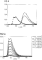
- FIG. 5a-c show the emission spectra for 20% by weight of FIrpic in mCP ( FIG. 5a ) 2% by weight of Ir (MDQ) 2 (acac) in mCP ( FIG. 5b ) and 20% by weight of FIrpic and 2% by weight of Ir (MDQ) 2 (acac) in mCP ( FIG. 5c ) at current densities of 0.5 mA / cm 2 to 8.75 mA / cm 2 .
- the CIE coordinates of the emitted light for a mCP with red emitter Ir (MDQ) 2 (acac) and for mCP with red emitter Ir (MDQ) 2 (acac) and exciton scavengers FIrpic are essentially unchanged: concentration Current [mA / cm 2 ] CIE coordinate x CIE coordinate y external quantum efficiency [ ⁇ ext ] 20% by weight of FIrpic in mCP 2.5 0.193 0.415 6.4% 2% by weight of Ir (MDQ) 2 (acac) in mCP 2.5 0.594 0.395 10.2% 20% by weight of FIrpic + 2% by weight of Ir (MDQ) 2 (acac) in mCP 2.5 0.591 0.392 14.7% 20 wt% FIrpic + 5 wt% Ir (MDQ) 2 (acac) in mCP 2.5 0.623 0,375 18.1%
- FIG. 5 it can be seen that the admixture also causes improved injection and transport across the FIrpic molecules, resulting in a much steeper current-voltage curve and lower operating voltages (open squares). These are similar to those with 20 wt% FIrpic without ADS 076 (filled squares), indicating that the electron transport in the mixed layer is enhanced by the introduction of the exciton scavenger.
- the cause of the in FIG. 3 The improvement in electricity efficiency shown can be seen in the fact that due to the higher concentration of the Thus, more excitons are formed on the exciton trap and then transferred to the emitter molecules.
- ADS 076 is present in low concentration and the transport from the FIrpic to the ADS 076 proceeds very efficiently and quickly, it is achieved thereby that with low concentration sequencing effects a good transfer of excitons to the desired emitter takes place. Therefore, there is an increase in the power efficiency.
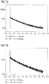
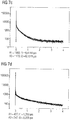
- FIGS. 6a to 6d shows the disintegration times of Ir (ppy) and ADS 076 in PMMA as a matrix.
- FIG. 6a shows the disintegration time of 5 wt% Ir (ppy) 3 . Measured here is the emission maximum at 510 nm. This results in a half-life of 1.0 ms.
- FIG. 6b shows for a sample with 1 wt .-% ADS 076 in PMMA, the disintegration time for the emission maximum at 595 nm. The half-life is 1.4 ⁇ s.
- the FIGS. 6c and 6d show an emitter layer with 1 wt% ADS 076 and 5 wt% Ir (ppy) 3 in PMMA.
- FIG. 6a shows the disintegration time of 5 wt% Ir (ppy) 3 . Measured here is the emission maximum at 510 nm. This results in a half-life of 1.0 ms.
- FIG. 6b shows for a sample with 1
- FIG. 6c shows the disintegration time for the emission maximum of the exciton scavenger at 510 nm. The result is a half-life of 0.4 ⁇ s, which is only 33% of the half-life for a sample containing only the matrix material and the exciton scavenger.
- FIG. 6d shows the spectrum for the emission maximum of ADS 076 at 595 nm; This results in a half-life of 1.3 ⁇ sec, which is barely changed compared to a sample containing only PMMA and ADS 076.
- the measurement of the half-lives is carried out according to V. O'Connor, D. Phillips, "Time Correlated single photon counting" (Academic Press, London 1987 ).
Landscapes
- Physics & Mathematics (AREA)
- Chemical & Material Sciences (AREA)
- Optics & Photonics (AREA)
- Engineering & Computer Science (AREA)
- Materials Engineering (AREA)
- Spectroscopy & Molecular Physics (AREA)
- Inorganic Chemistry (AREA)
- Crystallography & Structural Chemistry (AREA)
- Electroluminescent Light Sources (AREA)
Description
- Die vorliegende Erfindung betrifft eine strahlungsemittierende Vorrichtung, gemäß Anspruch 1, mit einer Emitterschicht, die ein Matrixmaterial, einen strahlungsemittierenden Emitter und einen phosphoreszenten Exzitonenfänger enthält.
- Diese Patentanmeldung beansprucht die Prioritäten der deutschen Patentanmeldung
DE 10 2008 063 589.8 und der deutschen PatentanmeldungDE 10 2008 050 331.2 . - Die Druckschrift
US 2005/074630 A1 , die DruckschriftUS 2004/137267 A1 und die die DruckschriftJP 2006 041395 A US 2006/232194 A1 eine hybride OLED mit phosphoreszierenden und fluoreszierenden Emittern. - Hoch effiziente, phosphoreszente Emitter sind eine der Voraussetzungen für die Entwicklung hoch effizienter organischer lichtemittierender Dioden (OLEDs) sowie für Display- und Lightinganwendungen. Entscheidend hierfür ist einerseits die Quanteneffizienz des einzelnen Emittermoleküls und andererseits des Emitters insgesamt, die Stromeffizienz sowie die Leistungseffizienz des Systems (das heißt die Lichtleistung pro elektrischer Leistung).
- Aufgabe der Erfindung ist es, eine strahlungsemittierende Vorrichtung mit verbesserter Effizienz bereitzustellen.
- Diese Aufgabe wird durch die Vorrichtung gemäß den unabhängigen Ansprüchen gelöst. Weitere Ausgestaltungen sind Gegenstand von Unteransprüchen.
- Die erfindungsgemäße strahlungsemittierende Vorrichtung umfasst ein Substrat, eine erste Elektrode und eine zweite Elektrode sowie eine zwischen der ersten und der zweiten Elektrode angeordnete Emitterschicht. Diese Emitterschicht weist ein Matrixmaterial auf, das 0,5 - 5 Gew.-% eines strahlungsemittierenden Emitters und 5 - 30 Gew.-% eines phosphoreszenten Exzitonenfängers enthält. Der Gewichtsanteil des Exzitonenfängers ist höher als der des strahlungsemittierenden Emitters. Weiterhin befindet sich das Emissionsmaximum des phosphoreszenten Exzitonenfängers bei einer kürzeren Wellenlänge als das Emissionsmaximum des strahlungsemittierenden Emitters. Die Stromeffizienz der Emitterschicht der strahlungsemittierenden Vorrichtung ist gegenüber der Stromeffizienz einer Emitterschicht, die keinen Exzitonenfänger enthält, um mindestens 10% erhöht.
- Durch die erfindungsgemäße Emitterschicht, die neben Matrixmaterial und strahlungsemittierendem Emitter auch einen phosphoreszenten Exzitonenfänger umfasst, ist die Stromeffizienz der Emitterschicht gegenüber einer Emitterschicht ohne Exzitonenfänger e. Die Leitungseigenschaften des Dotierstoffs führen nämlich zu einem besseren Ladungsträgergleichgewicht sowie zu einer geringeren Spannung; neben einer erhöhten Quanteneffizienz führt dies zu einer Verbesserung der Leistungseffizienz.
- Das bessere Ladungsträgergleichgewicht ist darauf zurückzuführen, dass die Matrix die Majoritätsladungsträger transportiert und der Exzitonenfänger die Minoritätsladungsträger (z.B. werden bei einer lochtranportierenden Matrix die Elektronen über das LUMO des Exzitonenfängers transportiert). Der Zusatz der Exzitonenfänger ermöglicht daher auch den Einsatz von Emittermaterialien, die nur in geringen Konzentrationen höchste Photolumineszenzeffizienten besitzen und dadurch zum Beispiel gute Langzeitstabilität aufweisen, also zum Einsatz für hoch effiziente OLEDs in Frage kommen. Diese Stoffe sind - wenn sie nicht in Mischung mit dem Exzitonenfänger vorliegen - weniger gut geeignet, da die wenigen im Matrixmaterial enthaltenen Emittermoleküle dann als Fallenzentren wirken, d.h. die Ladungsträgermobilität wird verringert (da die Ladungsträger auf den Fallenzentren "gefangen" sind). Dies hat zur Folge, dass die Betriebsspannung erhöht wird.
- Durch die niedrig konzentrierten Emittermaterialien kann auch verhindert werden, dass insbesondere bei Emittern ohne sterische Hinderung bei hohen Konzentrationen eine Stapelung der Moleküle auftritt, welche eine Rotverschiebung des emittierten Spektrums zur Folge haben kann. Die hohen Konzentrationen des Exzitonenfängers bewirken dagegen - neben den vorstehenden Effekten, dass diese Exzitonenfänger nicht als Fallenzentren für die Ladungsträger wirken, sondern dass ein guter Transport der Ladungsträger stattfinden kann.
- Die in den erfindungsgemäßen strahlungsemittierenden Vorrichtungen enthaltenen Emitterschichten weisen somit eine erhöhte Stromeffizienz (verglichen mit Emitterschichten ohne die erfindungsgemäßen Exzitonenfänger) auf, die um mindestens 10% erhöht ist (insbesondere bei Leuchtdichten von 10 bis 1100 cd/m2). Häufig liegt die Stromeffizienz sogar 20% und vielfach sogar 25% über der Stromeffizienz einer entsprechenden Emitterschicht ohne den erfindungsgemäßen Exzitonenfänger (insbesondere bei Leuchtdichten von 10 bis 1100 cd/m2). Dies gilt insbesondere für Stromeffizienzen bei hohen Lichtstärken, d.h. Lichtstärken, die typischerweise größer 1000 cd/m2 sind.
- Im Folgenden werden die einzelnen Komponenten der strahlungsemittierenden Vorrichtung der vorliegenden Erfindung näher erläutert:
- Ein "Substrat" umfasst gemäß der vorliegenden Erfindung zum Beispiel ein Substrat, wie es im Stand der Technik herkömmlich für eine strahlungsemittierende Vorrichtung verwendet wird. Beispielsweise kann das Substrat Glas, Quarz, Kunststofffolien, Metall, Metallfolien, Siliziumwafer oder
- ein anderes geeignetes Substratmaterial umfassen. Ist die strahlungsemittierende Vorrichtung zum Beispiel als so genannter "Bottom-Emitter" ausgeführt, ist das Substrat vorzugsweise transparent und beispielsweise als Glassubstrat ausgeführt.
- In der erfindungsgemäßen strahlungsemittierenden Vorrichtung kann die erste Elektrode auf dem Substrat abgeschieden sein.
- Die "erste Elektrode", wie sie hierin verwendet wird, kann zum einen eine Anode sein. Die Anode kann aus einem löcherinjizierenden Material bestehen. Als löcherinjizierendes Material kann jedes im Stand der Technik bekannte, löcherinjizierende Material verwendet werden. Ist die strahlungsemittierende Vorrichtung beispielsweise als "Bottom-Emitter" ausgebildet, so besteht die Anode üblicherweise aus einem transparenten Material. Beispielsweise kann sie aus transparenten leitenden Oxiden bestehen oder eine Schicht hieraus umfassen. Diese transparenten leitenden Oxide (transparent conductive oxides, "TCO") schließen Metalloxide, wie beispielsweise Zinkoxid, Zinnoxid, Cadmiumoxid, Titanoxid, Indiumoxid oder Indiumzinnoxid (ITO), Zn2SnO4, CdSnO3, ZnSnO3, MgIn2O4, GaInO3, Zn2In2O5 oder In4Sn3O12 oder Mischungen unterschiedlicher transparenter leitender Oxide ein, sind jedoch nicht auf diese beschränkt. Die TCOs unterliegen dabei nicht zwingend einer stöchometrischen Zusammensetzung und können ferner auch p- oder n-dotiert sein.
- Wenn die erste Elektrode eine Anode ist, ist die zweite Elektrode eine Kathode.
Die "Kathode" kann aus einem elektroneninjizierenden Material bestehen. Als Kathodenmaterialien können dabei im Stand der Technik übliche Kathodenmaterialien, insbesondere Aluminium, Barium, Indium, Silber, Gold, Magnesium, Calcium oder Lithium sowie Verbindungen, und Legierungen dieser Stoffe und Gemische der vorgenannten Elemente, Verbindungen und/oder Legierungen verwendet werden. Alternativ oder zusätzlich können auch eines oder mehrere der bei den Anoden-Materialien genannten TCOs enthalten sein bzw. kann die Kathode auch vollständig aus einem dieser Materialien bestehen. Die Kathode kann damit auch transparent ausgeführt sein. - In der strahlungsemittierenden Vorrichtung kann zum Beispiel eine Elektrode transparent und die andere reflektierend ausgeführt sein. Die strahlungsemittierende Vorrichtung kann somit entweder als "Bottom-Emitter" oder als "Top-Emitter" ausgeführt werden. Alternativ dazu können auch beide Elektroden transparent ausgeführt sein.
- Die Emitterschicht der erfindungsgemäßen strahlungsemittierenden Vorrichtung bezeichnet eine funktionelle Schicht aus einem Matrixmaterial, das einen oder mehrere strahlungsemittierende Emitter und einen oder mehrere phosphoreszente Exzitonenfänger enthält beziehungsweise aus dem Matrixmaterial, dem mindestens einen Emitter und dem mindestens einen Exzitonenfänger besteht.
- Der Emitter und der Exzitonenfänger können hierbei in ein Matrixmaterial eingebettet sein, das ausgewählt ist aus einer Gruppe, bestehend aus mCP (1,3-Bis(carbazol-9-yl)benzol), TCP (1,3,5-Tris(carbazol)-9-yl)benzol), TCTA (4,4',4"-Tris(carbazol-9-yl)triphenylamin), TPBi(1,3,5-tris(1-phenyl-1-H-benzimidazol-2-yl)benzol), CBP (4,4'-Bis(carbazol-9-yl)biphenyl), CDBP (4,4'-Bis(9-carbazolyl)-2,2'-dimethylbiphenyl), (DMFL-CBP 4,4'-Bis(carbazol-9-yl)-9,9-dimethylfluoren), FL-4CBP (4,4'-Bis(carbazol-9-yl)-9,9-bis(9-phenyl-9H-carbazol)fluoren), DPFL-CBP (4,4'-Bis(carbazol-9-yl)-9,9-ditolylfluoren), FL-2CBP (9,9-Bis(9-phenyl-9H-carbazol)fluoren), Spiro-CBP (2,2',7,7'-Tetrakis(carbazol-9-yl)-9,9'-spiro-bifluoren), ADN (9,10-Di(naphth-2-yl)anthracen, TBADN (3-Tert-butyl-9,10-di(naphth-2-yl)anthracen, DPVBi (4,4'-Bis(2,2-diphenyl-ethen-1-yl)-4,4'-dimethylphenyl), p-DMDPVBi (4,4'-Bis(2,2-diphenyl-ethen-1-yl)-4,4'-dimethylphenyl), TDAF (Tert(9,9-diarylfluoren)), BSBF (2-(9,9'-Spirobifluoren-2-yl)-9,9'-spirobifluoren), TSBF (2,7-Bis(9,9'-spirobifluoren-2-yl)-9,9'-spirobifluoren), BDAF Bis(9,9-diarylfluoren), p-TDPVBi (4,4'-Bis(2,2-diphenyl-ethen-1-yl)-4,4'-di-(tert-butyl)phenyl), TPB3 (1,3,5-Tri-(pyren-1-yl)benzol) sowie aus Gemischen der vorgenannten Stoffe. Als Matrixmaterial bevorzugt sind die Materialen TCTA, TPBi, CBP, CDBP und CPF. Als Matrixmaterialien die in gemischten System vorliegen, werden bevorzugt Mischungen aus einem oder mehreren der Materialien TCTA, mCP, CBP, CDBP oder CPF untereinander oder Mischungen mit TPBi verwendet.
- Das Emittermaterial kann beispielsweise ein Emissionsmaximum im blauen, grünen oder roten Spektralbereich aufweisen. Weist ein derartiges Emittermaterial mehrere Emissionsmaxima auf, so gilt als Emissionsmaximum im Sinne dieser Erfindung das Emissionsmaximum mit der größten Intensität.
- Existieren bei unterschiedlichen Stromstärken zwei oder mehr intensitätsstärkste Emissionsmaxima bei unterschiedlichen Wellenlängen, so gilt von diesen Emissionsmaxima im Sinne dieser Erfindung das Maximum bei der kleineren Wellenlänge als Emissionsmaximum (insbesondere für die Bestimmung der Differenz der Wellenlängen des Emissionsmaximums des strahlungsemittierenden Emitters und des Emissionsmaximums des Exzitonenfängers).
- Ein blau phosphoreszierendes Emittermaterial kann ausgewählt sein aus der Gruppe, bestehend aus FIrPic (Bis(3,5-difluoro-2-(2-pyridyl)phenyl-(2-carboxypyridyl)-iridium III), Flr6 (Bis(48,68-difluorophenylpyridinato)-tetrakis(1-pyrazolyl)borat-iridium III) sowie aus Gemischen der vorgenannten Stoffe. Die genannten Emittermaterialien haben ihr Emissionsmaximum im blauen Spektralbereich.
Grün phosphoreszierendes Emittermaterial kann ausgewählt sein aus der Gruppe, bestehend aus Ir(ppy)3 (Tris(2-phenylpyridin)iridium(III)), Ir(ppy)2(acac) (Bis(2-phenylpyridin)(acetylacetonat)iridium(II)), Iridium (III)-tris(2-(4-tolyl)pyridinato-N,C2), Tris(2-phenylpyridin)iridium (III), Tris(8-hydroxychinolato)aluminium (III), Tris(2-methyl,8-hydroxychinolato)aluminium (III), Tris(8-hydroxychinolato)gallium (III), Tris(3-methyl-1-phenyl-4-trimethyl-acetyl-5-pyrazolin)terbium (III) sowie aus Gemischen der vorgenannten Stoffe. Die genannten Emittermaterialien haben ihr Emissionsmaximum im grünen Spektralbereich. - Als rot phosphoreszierendes Emittermaterial kann ein Emittermaterial eingesetzt werden, das ausgewählt ist aus der Gruppe bestehend aus Ir(mdq)2(acac) (Bis(2-methyl-dibenzo[f,h]-chinoxalin)(acetylacetonat)iridium(III)), Eu(dbm)3(phen) (Tris(dibenzoylmethan)phenanthrolin-europium(III)), Ir(btp)2(acac) (Bis(2-benzo[b]thiophen-2-yl-pyridin) (acetylacetonat)iridium(III)), Ir(piq)2(acac) (Bis(1-phenylisochinolin) (acetylacetonat)iridium(III)), Ir(fliq)2(acac)-1 (Bis[1-(-9,9-dimethyl-9H-fluoren-2-yl)-isochinolin](acetylacetonat)iridium(III)), Ir(flq)2(acac)-2 (Bis[3-(9,9-dimethyl-9H-fluoren-2-yl)-isochinolin](acetylacetonat)iridium(III)), Ru(dtb-bpy)3*2(PF6)(Tris[4,4'-di-tert-butyl-(2,2')-bipyridin]ruthenium(III)komplex), Ir(2-phq)3 (Tris(2-phenylchinolin)iridium(III)), Ir(2-phq)2(acac)(Bis(2-phenylchinolin)(acetylacetonat)iridium(III)), Ir(piq)3 (Tris-(1-phenylisochinolin)iridium(III)), Iridium (III)-bis(2-(2'-benzothienyl)pyridinato-N,C3')(acetylacetonat), Tris(dibenzoylacetonato)-mono(phenanthrolin)-europium (III), Tris(dibenzoylmethan)-mono(phenanthrolin)-europium (III), Tris(dibenzoylmethan)-mono(5-aminophenanthrolin)-europium (III), Tris(dinaphthoylmethan)-mono(phenanthrolin)-europium (III), Tris(4-brombenzoylmethan)-mono(phenanthrolin)-europium (III), Tris(dibiphenoylmethan)-mono(phenanthrolin)-europium (III), Tris(dibenzoylmethan)-mono(4,7-dimethylphenanthrolin)-europium (III), Tris(dibenzoylmethan)-mono(4,7-dimethylphenanthrolin-disulfonsäure)-europium (III)-dinatriumsalz, Tris[di(4-(2-(2-thoxyethoxy)ethoxy)benzoyl-methan)]-mono(phenanthrolin)-europium (III), Tris[di(4-(2-(2-thoxyethoxy)ethoxy)benzoylmethan)]-mono(5-aminophenanthrolin)-europium (III) sowie aus Gemischen der vorgenannten Stoffe. Die genannten Emittermaterialien haben ihr Emissionsmaximum im roten Spektralbereich.
- Weiterhin können als Emittermaterialien auch fluoreszierende Emitter eingesetzt werden.
- Als blau fluoreszierender Emitter kann dabei eine Verbindung eingesetzt werden, die ausgewählt ist aus der Gruppe, bestehend aus BCzVBi (4,4'-Bis(9-ethyl-3-carbazovinylen)-1,1'-biphenyl), Perylen, TBPe (2,5,8,11-Tetra-tert-butylperylen), BCzVB (9H-Carbazol-3,3'-(1,4-phenylen-di-2,1-ethendiyl)bis[9-ethyl-(9C)]), DPAVBi 4,4-Bis[4-(di-p-tolylamino)styryl]biphenyl, DPAVB (4-(Di-p-tolylamino)-4'-[(di-p-tolylamino)styryl]stilben), BDAVBi (4,4'-Bis[4-(diphenylamino)styryl]biphenyl), BNP3FL (N,N'-Bis(naphthalen-2-yl)-N,N'-bis(phenyl)-tris-(9,9-dimethylfluorenylen), 9,10-Bis[(9-ethyl-3-carbazoyl)-vinylenyl]-anthracen, 4,4'-Bis(diphenylvinylenyl)-biphenyl, 1,4-Bis(9-ethyl-3-carbazovinylen)-2-methoxy-5-(2-thylhexyloxy)benzol, 4,4'-Bis(diphenylvinylenyl)-anthracen, 1,4-Bis(9-ethyl-3-carbazovinylen)-9,9-dihexyl-fluoren sowie aus Gemischen der vorgenannten Stoffe. Die genannten Emittermaterialien haben ihr Emissionsmaximum im blauen Spektralbereich. Weiterhin können auch rot oder grün fluoreszierende Emittermaterialien eingesetzt werden.
- Die Emitterschicht der erfindungsgemäßen strahlungsemittierenden Vorrichtung weist neben dem strahlungsemittierenden Emitter auch noch einen phosphoreszenten Exzitonenfänger auf.
- Bei dem phosphoreszenten Exzitonenfänger handelt es sich um eine Verbindung, auf die ein effizienter Energieübertrag vom Matrixmaterial möglich ist. Im Betrieb werden daher zunächst Exzitonen vom Matrixmaterial auf den Exzitonenfänger übertragen beziehungsweise direkt auf diesem gebildet. Dem Exzitonenfänger kommt dann die Aufgabe zu, einen effizienten und schnellen Energieübertrag auf das Emittermaterial zu gewährleisten. Es werden Exzitonen auf dieses Emittermaterial übertragen.
- Der phosphoreszente Exzitonenfänger ermöglicht ferner einen guten Transport der Minoritätsladungsträger in einer Matrix, in der die Majoritätsladungsträger mit entgegengesetzter Ladung transportiert werden (bei einem lochtransportierenden Wirtsmaterial ermöglichen die Exzitonenfänger also einen guten Elektronentransport).
- Obwohl der Exzitonenfänger eine phosphoreszente Verbindung ist, kommt es also nicht darauf an, dass der Exzitonenfänger Strahlung emittiert; vielmehr ist es wesentlich, dass der Exzitonenfänger einen guten Transport sowohl der Ladungsträger als auch der Exzitonen gewährleistet. Die als Exzitonenfänger verwendeten Materialien unterscheiden sich stets von den als Emitter eingesetzten Materialien.
- Als Exzitonenfänger sind weitesgehend dieselben Verbindungen wie für die vorstehend genannten phosphoreszenten Emittermaterialien geeignet, sofern das Emissionsmaximum des phosphoreszenten Exzitonenfängers bei einer kürzeren Wellenlänge als das Emissionsmaximum des strahlungsemittierenden Emitters liegt.
- In einer Ausführungsform beträgt der Anteil des Exzitonenfängers 10 - 20 Gew.-% (im Rahmen der vorliegenden Erfindung beziehen sich alle Angaben in Gew.-% stets auf das in der Emitterschicht enthaltene Matrixmaterial). Ab einem Gewichtsanteil von mindestens 10 Gew.-% ist im Matrixmaterial soviel Exzitonenfänger enthalten, dass ein sehr effizienter Transport der Ladungsträger ermöglicht wird und daher ein deutlicher Anstieg der Stromeffizienz zu verzeichnen ist. Ab einem Anteil von 20 Gew.-% kann es unter Umständen dazu kommen, dass durch Wechselwirkungen von zwei Exzitonen Effizienzverluste erfolgen.
- In einer weiteren Ausführungsform ist der Anteil des strahlungsemittierenden Emitters 1 - 4 Gew.-%. Ab einem Gewichtsanteil von 5 Gew.-% ist mit einem Konzentrationsquenching und daher einer deutlich sinkenden Effizienz zu rechnen.
- In weiteren Ausführungsformen ist der Gewichtsanteil des Exzitonenfängers zumindest viermal, häufig sogar achtmal, so hoch wie der des strahlungsemittierenden Emittermaterials. In einer weiteren Ausführungsform liegt entweder das HOMO des Exzitonenfängers so, dass - sofern das Matrixmaterial ein Material ist, das Elektronen besser transportiert - eine Injektion der Löcher (d.h. ein Übertrag der Löcher von der anodenseitig auf die Emitterschicht folgenden Schicht auf die Exzitonenfänger) erleichtert wird oder es liegt das LUMO des Exzitonenfängers so, dass - sofern das Matrixmaterial ein Material ist, das Löcher besser transportiert - eine Injektion von Elektronen (von der kathodenseitig auf die Emitterschicht folgenden Schicht auf die Exzitonenfänger) erleichtert wird. Insbesondere liegt daher das LUMO des Exzitonenfängers bei einem besser lochtransportierenden Matrixmaterial um bis zu 0,3 Elektronenvolt über oder unter dem LUMO der kathodenseitig auf die Emitterschicht folgenden Schicht. Bevorzugt liegt das LUMO um 0 - 0,3 Elektronenvolt unter diesem Energieniveau. Bei besser elektronenleitenden Matrixmaterialien liegt das HOMO des Exzitonenfängers bevorzugt um bis zu 0,3 Elektronenvolt unter oder über dem HOMO der anodenseitig auf die Emitterschicht folgenden Schicht. Besonders bevorzugt ist ein HOMO, das 0 - 0,3 Elektronenvolt unter dem HOMO dieser Schicht liegt.
HOMO steht hierbei für "Highest Occupied Molecular Orbital" und LUMO für "Lowest Unoccupied Molecular Orbital". - Kathodenseitig kann beispielsweise eine Elektronentransportschicht auf die Emitterschicht folgen; anodenseitig kann beispielsweise eine Lochtransport-Schicht auf die Emitterschicht folgen.
- In einer weiteren Ausführungsform beträgt die Differenz der Wellenlängen des Emissionsmaximums des strahlungsemittierenden Emitters und des Emissionsmaximums des Exzitonenfängers mindestens 15 nm, üblicherweise sogar mindestens 30 nm. Üblicherweise wird für Emittermaterialien, die im gelben, orangen oder roten Spektralbereich emittieren, ein Exzitonenfänger eingesetzt, der ein Emissionsmaximum im blauen oder grünen Spektralbereich aufweist; für grün emittierende Emittermaterialien wird ein Exzitonenfänger, der ein Emissionsmaximum im blauen Spektralbereich aufweist eingesetzt und für blau emittierende Emittermaterialen ein Exzitonenfänger, der im violetten oder ultravioletten Spektralbereich das Emissionsmaximum aufweist. Insbesondere bei blau emittierenden Emittermaterialien beträgt die Differenz der Wellenlängen der Emissionsmaxima maximal 100 nm. Als roter, oranger, gelber, grüner, blauer und violetter Spektralbereich gelten erfindungsgemäß generell folgende Bereiche: roter Spektralbereich etwa 640 bis 780 nm; oranger Spektralbereich etwa 600 bis 640 nm, gelber Spektralbereich etwa 570 bis 600 nm, grüner Spektralbereich etwa 500 bis 570 nm, blauer Spektralbereich etwa 430 bis 500 nm, violetter Spektralbereich etwa 380 bis 430 nm.
- In einer weiteren Ausführungsform wird die von der Emitterschicht der erfindungsgemäßen strahlungsemittierenden Vorrichtung emittierte Strahlung im Wesentlichen durch den strahlungsemittierenden Emitter erzeugt. Aufgrund der sehr guten Ladungsträger und Exzitonenleitfähigkeit des Exzitonenfängers werden die in Matrixmaterial oder auf dem Exzitonenfänger gebildeten Exzitonen im Wesentlichen auf das Emittermaterial übertragen, so dass das von der Emitterschicht emittierte Licht im Wesentlichen denselben Farbeindruck hervorruft wie das Licht, das von einer Emitterschicht ohne Exzitonenfänger emittiert wird, hervorruft. Unter einem im Wesentlichen gleichen Farbeindruck wird hierbei insbesondere verstanden, dass die CIE-Koordinaten des emittierten Lichts einer Emitterschicht ohne Exzitonenfänger (xoE, yoE) sich nicht wesentlich von denen einer Emitterschicht mit Exzitonenfänger (xmE, ymE) unterscheiden. Im Regelfall gilt für die Differenz Δx = xoE - xmE bzw. die Differenz Δy = yoE - ymE, dass Δx < 0,05 und/oder Δy < 0,05. Häufig gilt sogar Δx < 0,03 und/oder Δy < 0,03 und vielfach auch Δx < 0,01 und/oder Δy < 0,01. Für die Summe der Absolutbeträge dieser Differenzen ∑Δ = |Δx| + |Δy| gilt im Regelfall ∑Δ < 0,08, häufig gilt ∑Δ < 0,05 und vielfach auch ∑Δ < 0,01.
- Vielfach ist bereits anhand des normalisierten Emissionsspektrums erkennbar, dass die Exzitonen vom Exzitonenfänger auf den strahlungsemittierenden Emitter übertragen werden. Üblicherweise beträgt nämlich die Intensität der normalisierten Emission des Emissionsmaximums des Exzitonenfängers in einem für die Emitterschicht mit Exzitonenfänger und strahlungsemittierendem Emitter gemessenen Spektrum maximal 10% der Intensität des Emissionsmaximums des strahlungsemittierenden Emitters. Die Intensität des Emissionsmaximums des Exzitonenfängers liegt bei maximal 5%, häufig sogar bei maximal 1%, der Intensität des Emissionsmaximums des strahlungsemittierenden Emitters. Die gemessenen Intensitätsverhältnisse sind hierbei üblicherweise unabhängig von der Stromdichte, insbesondere bei Stromdichten zwischen 0,5 und 10 mA/cm2.
- Üblicherweise ist es zudem so, dass auch die Intensität des Emissionsmaximums des Exzitonenfängers in einer Emitterschicht mit Exzitonenfänger und strahlungsemittierendem Emitter deutlich gegenüber der Intensität des Emissionsmaximums einer Emitterschicht, die nur den Exzitonenfänger (in gleicher Konzentration wie im vorstehend genannten "gemischten" System) und kein strahlungsemittierendes Emittermaterial enthält, reduziert ist. Die (bei gleicher Stromdichte von z.B. 5 mA/cm2 gemessene) Intensität der normalisierten Emission des Emissionsmaximums des Exzitonenfängers in der Emitterschicht mit Emitter und Exzitonenfänger beträgt maximal 5% der normalisierten Emission des Emissionsmaximums des Exzitonenfängers in einer Schicht, die nur aus dem Matrixmaterial und dem Exzitonenfänger besteht. Üblicherweise beträgt die (bei gleicher Stromdichte von z.B. 5 mA/cm2 gemessene) Intensität der normalisierten Emission des Emissionsmaximums des Exzitonenfängers in der Emitterschicht mit Emitter und Exzitonenfänger dann maximal 10%, und häufig sogar maximal 1% der normalisierten Emission des Emissionsmaximums des Exzitonenfängers in einer Schicht, die nur aus dem Matrixmaterial und dem Exzitonenfänger besteht. Wie vorstehend beschrieben wurde, ist dies im Wesentlichen auf die gute Exzitonenleitfähigkeit des Exzitonenfängers zurückzuführen.
- Die gute Exzitonenleitfähigkeit kann auch anhand der zeitaufgelösten wellenlängenabhängigen Emissionsspektren bestimmt werden. Vergleicht man hier eine Emitterschicht, die einen Exzitonenfänger und ein strahlungsemittierendes Emittermaterial enthält, mit einer identischen Schicht, die in denselben Konzentrationen jeweils nur den Exzitonenfänger beziehungsweise nur das strahlungsemittierende Emittermaterial enthält, so stellt man fest, dass sich die Halbwertszeit der Intensität der Emission des Emissionsmaximums des Exzitonenfängers im "gemischten System" deutlich reduziert hat während die Halbwertszeit der Intensität der Emission des Emissionsmaximums des strahlungsemittierenden Emittermaterials im Wesentlichen gleich bleibt. Häufig ist zu beobachten, dass sich die Halbwertszeit um mindestens die Hälfte reduziert. Oft beträgt die Halbwertszeit sogar nur 40% und vielfach sogar nur 33% der Halbwertszeit, die für ein Matrixmaterial, in dem ausschließlich der Exzitonenfänger enthalten ist, gemessen wurde. Dieser Effekt bedeutet unter anderem auch, dass die Lebensdauer der Exzitonen auf dem strahlungsemittierenden Emitter im Regelfall länger ist als die Lebensdauer der Exzitonen auf dem Exzitonenfänger. Vergleicht man diese Lebensdauer mit den Lebensdauern von Matrixmaterialien, in die jeweils ausschließlich der Exzitonenfänger oder das strahlungsemittierende Emittermaterial in gleicher Konzentration enthalten ist, so stellt man fest, dass in den nicht "gemischten Systemen" genau die umgedrehte Situation vorliegen kann, also die Lebensdauer der Exzitonen auf dem Exzitonenfänger länger sein kann, als die der Exzitonen im parallelen System auf dem strahlungsemittierenden Emitter.
- Die vorstehend beschriebenen Effekte führen im Regelfall auch dazu, dass die externe Quanteneffizienz der Emitterschicht deutlich erhöht werden kann. Vergleicht man die externe Quanteneffizienz einer Emitterschicht mit Exzitonenfänger und strahlungsemittierendem Emitter mit der Quanteneffizienz einer Emitterschicht, die nur den strahlungsemittierenden Emitter (in der gleichen Konzentration) und keinen Exzitonenfänger enthält, so stellt man fest, dass die Quanteneffizienz zumeist um mindestens 20% erhöht ist. Häufig kann sogar eine Erhöhung um 30% festgestellt werden. Mit der erfindungsgemäßen Emitterschicht können daher externe Quanteneffizienzen ηext größer 12%, häufig sogar größer 14% erreicht werden. Es können sogar Quanteneffizienzen zwischen über 18%, z.B. von 20% erreicht werden.
- In einer weiteren Ausgestaltung weist der in der Emitterschicht enthaltene strahlungsemittierende Emitter eine hohe Photolumineszenzquantenausbeute auf, insbesondere auch bei niedrigen Emitterkonzentrationen. Im Regelfall wird diese Photolumineszenzquantenausbeute ηPL niedriger sein als die des Exzitonenfängers. Weiterhin besitzen auch die Exzitonen auf dem strahlungsemittierenden Emittermaterial eine relativ kurze Lebensdauer. Im Regelfall beträgt diese maximal 20 µs.
- In einer weiteren Ausgestaltung weist das strahlungsemittierende Emittermaterial ein LUMO auf, das über dem LUMO des Exzitonenfängers liegt. Dies führt dazu, dass die Exzitonen im Wesentlichen vom Exzitonenfänger eingefangen beziehungsweise auf diesem gebildet werden und der Exzitonenfänger beziehungsweise das strahlungsemittierende Emittermaterial im Wesentlichen die Aufgaben erfüllen können, die ihnen zugedacht sind. Es erfolgt dann im Wesentlichen eine Übertragung der im Matrixmaterial gebildeten Exzitonen auf den Exzitonenfänger und nicht auf das strahlungsemittierende Emittermaterial, das wiederum besonders effizient dazu dienen kann, Strahlung zu emittieren. Die Erfindung ist allerdings nicht hierauf beschränkt, vielmehr kann das LUMO des strahlungsemittierenden Emitters auch unter dem des Exzitonenfängers liegen. Weiterhin können des LUMO des Exzitonenfängers und gegebenenfalls auch des strahlungsemittierenden Emitters niedriger als das des Matrixmaterials liegen. Dies führt dazu, dass die Exzitonen verstärkt auf dem Exzitonenfänger gebildet werden und daher der Schritt der Übertragung der auf der Matrix gebildeten Exzitonen auf den Exzitonenfänger entfällt.
- In einer weiteren Ausgestaltung hat die Emitterschicht der strahlungsemittierenden Vorrichtung eine Schichtdicke von 10 - 40 nm. Emitterschichten mit geringeren Schichtdicken sind schwerer zu prozessieren; außerdem kann ab einer Schichtdicke von 10 nm die Anzahl der Emitterzentren optimiert werden und damit besser an die Lebensdauer der Exzitonen angepasst werden. Im Einzelfall kann aber auch eine Schichtdicke zwischen 5 und 10 nm technisch sinnvoll sein. Für die Herstellung einer weißes Licht emittierenden strahlungsemittierenden Vorrichtung, die mehrere Emitterschichten enthält, beträgt die Schichtdicke der einzelnen Emitterschichten bevorzugt jeweils 10 - 15 nm.
- Üblicherweise ist der Emitter und auch der Exzitonenfänger statistisch über das Matrixmaterial verteilt. Allerdings können auch Konzentrationsgradienten in der Emitterschicht vorliegen, so dass sich beispielsweise Bereiche, in denen der Exzitonenfänger höher konzentriert ist mit Bereichen, in denen das Emittermaterial im Verhältnis höher konzentriert ist abwechseln; es können in der Emitterschicht sogar auch nur Bereiche vorliegen, in denen ausschließlich Exzitonenfänger enthalten ist und Bereiche in denen ausschließlich der phosphoreszente Emitter enthalten ist.Hiermit können gezielt Zonen eingestellt werden, in denen entweder Exzitonen gebildet werden beziehungsweise Zonen, in denen die Emission erfolgt.
- Die strahlungsemittierende Vorrichtung weist eine weitere Emitterschicht, häufig insgesamt zumindest zwei oder drei Emitterschichten, auf. Hierbei enthält eine Emitterschicht - wie die erste Emitterschicht - neben dem strahlungsemittierenden Emitter auch einen Exzitonenfänger. Mehrere der weiteren Emitterschichten - wie die erste Emitterschicht - können neben dem strahlungsemittierenden Emitter auch einen Exzitonenfänger enthalten. Für diese weiteren Emitterschichten gelten die vorstehend für die erste Emitterschicht gemachten Ausführungen entsprechend.
- Es liegen zwischen jeweils zwei der Emitterschichten Blockierschichten vor. Enthält die strahlungsemittierende Vorrichtung mehr als zwei Emitterschichten, so kann zwischen allen Emitterschichten eine Blockierschicht vorliegen aber auch nur zwischen einem Teil der Emitterschichten. Eine solche Blockierschicht dient zum Blockieren von Exzitonen. Eine solche Blockierschicht kann dabei so gestaltet sein, dass ihre Dicke größer ist als die mittlere freie Weglänge der in der jeweils benachbarten Schicht gebildeten Exzitonen, so dass diese im Wesentlichen nicht in die zweite Schicht gelangen können. Ferner kann die Blockierschicht alternativ oder gleichzeitig auch zumindest in Teilen der Schicht zum Blockieren von Ladungsträgern (Elektronen oder Löchern) dienen. Durch Schichten oder Teilbereiche von Schichten, die Ladungsträger blockieren kann eine gezielte Einstellung der Ladungsträgerdichte erfolgen. Eine Blockierschicht zum Blockieren von Exzitonen und/oder Ladungsträgern kann ein oder mehrere Matrixmaterialien umfassen oder hieraus bestehen, wobei geeignete Matrixmaterialien aus den vorstehend offenbarten Matrixmaterialien ausgewählt werden können. Alternativ können Schichten die Elektronen blockieren eines oder mehrere der nachfolgenden Materialien für Lochtransport-Schichten umfassen oder diese(s) und ein oder mehrere Matrixmaterialien umfassen. Ferner können Schichten die Löcher blockieren eines oder mehrere der nachfolgenden Materialien für Elektronentransport-Schichten umfassen oder diese(s) und ein oder mehrere Matrixmaterialien umfassen.
- In einer weiteren Ausgestaltung emittiert die erfindungsgemäße strahlungsemittierende Vorrichtung Weißlicht. Dieses Weißlicht kann gebildet werden durch die Überlagerung der Strahlung, die durch die erste Emitterschicht und die zumindest eine weitere Emitterschicht emittiert wird. Üblicherweise werden hierfür zumindest drei Emitterschichten (zum Beispiel Emitterschichten die jeweils im roten, grünen und blauen Spektralbereich emittieren) verwendet. Denkbar ist allerdings auch ein System, das nur zwei Emitterschichten enthält (beispielsweise eine blau und eine orange emittierende Schicht).
- Zusammenfassend kann festgestellt werden, dass erfindungsgemäß erkannt wurde, dass durch die Kombination eines phosphoreszenten Exzitonenfängers in hoher Konzentration und eines Emittermaterials in niedriger Konzentration unabhängig voneinander zwei Effekte realisiert werden können. Zum einen werden durch dieses gemischte System im Betrieb zunächst Exzitonen vom Matrixmaterial auf den Exzitonenfänger übertragen beziehungsweise auf dem Exzitonenfänger gebildet. Durch einen effizienten und schnellen Energieübertrag gelangen die Exzitonen dann auf das Emittermaterial, auf dem sie effizient, strahlend zerfallen können. Außerdem weist der Exzitonenfänger hervorragende Leitungseigenschaften für die Minoritätsladungsträger auf. Beide Effekte führen insgesamt zu einem besseren Ladungsträgergleichgewicht und zu einer geringeren Spannung, was neben der erhöhten Quanteneffizienz zu einer weiteren Verbesserung der Leistungseffizienz beiträgt. Durch das erfindungsgemäße System ist es auch möglich, dass nicht ein spezifisches optimiertes Matrix/Emittermaterial-System zum Einsatz kommen muss, sondern ein weiterer Parameter existiert, der die Bandbreite der verwendbaren Matrixmaterialien vergrößert.
- Die strahlungsemittierende Vorrichtung kann auch weitere funktionelle Schichten aufweisen. Solche Schichten können beispielsweise Elektronentransportschichten, Elektroneninjektionsschichten, Lochtransportschichten und/oder Lochinjektionsschichten sein. Solche Schichten können dazu dienen, die Effizienz der strahlungsemittierenden Vorrichtung weiter zu steigern und an einer oder mehreren geeigneten Stellen der strahlungsemittierenden Vorrichtung ausgebildet werden. Sie können geeignete Elektronentransportmaterialien und/oder Lochtransportmaterialien und/oder zur Verbesserung der Lochinjektion geeignete Materialien umfassen.
- Als Elektronentransportmaterialien seien beispielsweise Liq (8-Hydroxychinolinolato-lithium), TPBi (2,2',2"-(1,3,5-Benzintriyl)-tris(1-phenyl-1-H-benzimidazol)), PBD (2-(4-Biphenylyl)-5-(4-tert-butylphenyl)), BCP (2,9-Dimethyl-4,7-diphenyl-1,10-phenanthrolin), BPhen (4,7-Diphenyl-1,10-phenanthrolin), BAlq (Bis-(2-methyl-8-chinolinolat)-4-(phenylphenolato)aluminium) und TAZ (3-(4-Biphenylyl)-4-phenyl-5-tert-butylphenyl-1,2,4-triazol) sowie Gemische der vorgenannten Stoffe genannt. Für die Elektronentransportschicht (die zugleich als Exzitonen-Blockierschicht dienen kann) werden bevorzugt Stoffe ausgewählt aus der Gruppe, bestehend aus TPBi, BCP, Bphen, CzSi und TAZ sowie aus Gemischen dieser Stoffe.
- Als Lochtransportmaterialien seien zum Beispiel NPB (N,N'-Bis(naphthalen-1-yl)-N,N'-bis(phenyl)-benzidin, β-NPB (N,N'-Bis(naphthalen-2-yl)-N,N'-bis(phenyl)-benzidin), TPD (N,N'-Bis(3-methylphenyl)-N,N'-bis(phenyl)-benzidin), Spiro-TPD (N,N'-Bis(3-methylphenyl)-N,N'-bis(phenyl)-benzidin), Spiro-NPB (N,N'-Bis(naphthalen-1-yl)-N,N'-bis(phenyl)-spiro), DMFL-TPD (N,N'-Bis(3-methylphenyl)-N,N'-bis(phenyl)-9,9-dimethylfluoren, DMFL-NPB (N,N'-Bis(naphthalen-1-yl)-N,N'-bis(phenyl)-9,9-dimethylfluoren), DPFL-TPD (N,N'-Bis(3-methylphenyl)-N,N'-bis(phenyl)-9,9-diphenylfluoren), DPFL-NPB (N,N'-Bis(naphthalen-1-yl)-N,N'-bis(phenyl)-9,9-diphenylfluoren), Sp-TAD (2,2',7,7'-Tetrakis(n,n-diphenylamino)-9,9'-spirobifluoren) und TAPC (Di-[4-(N,N-ditolyl-amino)-phenyl]cyclohexan) oder Gemische der vorgenannten Stoffe genannt. Für die Lochtransport-Schicht (die ebenfalls gleichzeitig als Exzitonen-Blockierschicht dienen kann) werden bevorzugt Stoffe ausgewählt aus der Gruppe, bestehend aus NPB, TCTA, TPD, Sp-TAD und TAPC sowie aus Gemischen dieser Stoffe.
- Als zur Verbesserung der Lochinjektion geeignete Materialien, seien beispielsweise CuPC (Phthalocyanin, Kupferkomplex), TiOPC (Titanoxidphthalocyanin), m-MTDATA (4,4',4"-Tris(N-3-methylphenyl-N-phenylamino)triphenylamin), 2T-NATA (4,4',4"-Tris(N-(2-naphthyl)-N-phenyl-amino)triphenylamin), IT-NATA (4,4',4"-Tris(N-(1-naphthyl)-N-phenylamino)triphenylamin), NATA (4,4',4"-Tris(N,N-diphenylamino)triphenylamin) sowie Gemische der vorgenannten Stoffe genannt, wobei die angegebenen Materialien optional dotiert sein können.
- Im Folgenden wird die vorliegende Erfindung anhand von Beispielen und Figuren beschrieben.
-
Figur 1 zeigt eine schematische Übersicht über eine strahlungsemittierende Vorrichtung gemäß der vorliegenden Erfindung. -
Figur 2 zeigt eine schematische Darstellung der Energieniveaus einer Ausführungsform einer OLED-Struktur. -
Figur 3 zeigt die verbesserte Stromeffizienz der Emitterschicht in Abhängigkeit von der Leuchtdichte. -
Figur 4 zeigt das Elektrolumineszenz-Spektrum für Emitterschichten mit und ohne Exzitonenfänger bzw. mit und ohne Emitter bei einer Stromdichte von 5 mA/cm2. - Die
Figuren 5a bis 5c zeigen das Elektrolumineszenz-Spektrum für Schichten mit und ohne Exzitonenfänger bzw. mit und ohne Emitter bei verschiedenen Stromdichten. -
Figur 5 zeigt die Verbesserung der Strom-Spannungs-Charakteristik. - Die
Figuren 6a bis 6d zeigen zeit- und wellenlängenaufgelöste Emissionsspektren. - Die
Figur 1 zeigt den schematisierten Schichtaufbau eines organischen selbstemittierenden Bauteils. Von unten nach oben ist folgender Schichtaufbau realisiert: Zu unterst befindet sich das Substrat 1, das beispielsweise transparent sein kann und auch aus Glas sein kann. Darauf befindet sich eine untere Elektrodenschicht 2, die beispielsweise ein transparentes leitendes Oxid wie Indium-Zinn-Oxid (ITO) sein kann. Die untere Elektrodenschicht kann dabei als Anode oder als Kathode fungieren. Über diese Elektrodenschicht 2 liegt eine Lochinjektionsschicht 3 über der wiederum eine Lochtransport-Schicht 4 angeordnet ist. Über der Lochtransport-Schicht 4 ist die organisch aktive Schicht, die Emissionsschicht 5, angeordnet. Es folgen auf die erste Emissionsschicht die weitere Emissionsschicht, die durch Exzitonen-Blockierschichten getrennt sind. Auf der einen Emissionsschicht liegt die lochblockierende Schicht 6, auf der die Elektronentransportschicht 7 und schließlich die Elektroneninjektionsschicht 8 mit angrenzender oberer Elektrode 9 angeordnet sind. Die obere Elektrode 9 kann beispielsweise eine Metallelektrode oder eine weitere transparente Elektrode, zum Beispiel aus einem der vorstehend genannten transparenten leitenden Oxide sein. - Bei Anlegen einer Spannung zwischen oberer und unterer Elektrode fließt Strom durch das Bauteil und in der organisch aktiven Schicht werden Photonen freigesetzt, die in Form von Licht über die transparente Elektrode beziehungsweise die transparenten Elektroden das Bauteil verlassen.
- In der Emissionsschicht 5 sind erfindungsgemäß in einer Matrix ein oder mehrere Exzitonenfänger und ein oder mehrere strahlungsemittierende Emitter (letztere jeweils in niedriger Konzentration) vorgesehen.
- Die Herstellung eines derartigen strahlungsemittierenden Bauelements kann zum Beispiel folgendermaßen erfolgen: Mittels HF-Sputtern wird zunächst eine ITO-Schicht als Anode auf einer Glasplatte abgeschieden. Zur Abscheidung der weiteren funktionellen Schichten wird dieses Substrat in einen Rezipienten eingebracht; dieser enthält mehrere Quellen, in denen organisches Material (insbesondere zur Verwendung als Exzitonenfänger sowie zur Verwendung als strahlungsemittierender Emitter) zur Herstellung der einzelnen funktionellen Schichten der strahlungsemittierenden Vorrichtung verdampft werden kann. Ferner werden eine oder mehrere Quellen für die Zuführung von einem oder mehreren verschiedenen Matrixmaterialien vorgesehen. Zur Ausbildung einer Lochinjektionsschicht wird aus einer Quelle mit Matrixmaterial und einer Quelle mit einem P-Dotanden gemeinsam auf der Glasplatte, auf der bereits die Anode vorliegt, abgeschieden. Entsprechend erfolgt die gemeinsame Abscheidung von Dotand und Matrixmaterial für die Lochtransport-Schicht. Anschließend erfolgt die gemeinsame Abscheidung eines Matrixmaterial, die zur erfindungsgemäßen Emitterschicht führt. Hierfür werden ein Matrixmaterial, der Exzitonenfänger und das mindestens eine strahlungsemittierende Emittermaterial gemeinsam abgeschieden. Die Abscheidung weiterer enthaltener Schichten wie Blockierschicht, Elektronentransportschicht und Elektroneninjektionsschicht erfolgt analog. Abschließend wird eine Aluminiumschicht als reflektierende Elektrode gebildet. Alternativ können (abgesehen von den Elektrodenschichten) die verschiedenen funktionellen Schichten auch mittels eines Nassprozesses (z.B. Spincoating) aufgebracht werden, dies kann insbesondere sinnvoll sein, wenn die aufzubringende Schicht ein Polymer enthält. Weiterhin können auch die zuerst aufgebrachten Schichten mittels eines Nassprozesses und alle darauf angeordneten Schichten mittels Aufdampfen.
- Im Folgenden wird ein Ausführungsbeispiel zur Herstellung einer OLED, die rotes Licht emittiert, angegeben (nicht Teil dieser Erfindung). Die schematische Struktur dieser rot emittierenden OLED ist in
Figur 2 abgebildet. - Die rotes Licht emittierende OLED weist eine Lochtransport-Schicht aus NPB und eine Elektronentransportschicht aus TPBi, die jeweils 30 nm dick sind, auf. Auf der Lochtransport-Schicht ist eine Exzitonen-Blockierschicht aus TCTA angeordnet, um einen Transfer der Exzitonen aus der Emissionsschicht auf die weniger effiziente Lochtransport-Schicht zu vermeiden. Auch das auf der Kathode angeordnete TPBi fungiert als Blockierschicht für Exzitonen. Die Emissionsschicht selbst besteht aus dem Matrixmaterial mCP, in das der rot phosphoreszierende Emitter Ir(MDQ)2(acac), auch ADS 076 genannt (Energienieveaus in
Fig. 2 durch Punkte gekennzeichnet), und der hellblau phosphoreszierende Exzitonenfänger FIrpic (Energienieveaus inFig. 2 durch Quadrate gekennzeichnet) eingebracht sind. Aufgrund der Triplettniveaus der Moleküle führt dies dazu, dass nach der Bildung eines Exzitons auf dem Matrixmaterial dieses auf den Exzitonenfänger und bei passender Konzentration auf ADS 076 übertragen wird. Der Exzitonenfänger liegt daher beispielsweise in einer Konzentration von 20 Gew.-% vor, was neben einer guten direkten Exzitonenbildung auf dem Dotierstoff zu einem sehr guten Transfer auf dem Matrixmaterial gebildeten Exzitonen führt. Des Weiteren können die Exzitonen aufgrund der hohen Konzentration gut über die Exzitonenfänger-Moleküle zu dem Emittermaterial diffundieren und dort übertragen werden. Aufgrund der Lage des LUMOs des Exzitonenfängers FIrpic in Bezug auf das LUMO der Elektronentransportschicht findet auch eine sehr gute Elektroneninjektion und wegen der guten Elektronenleitfähigkeit des Exzitonenfängers außerdem ein sehr guter Elektronentransport statt. Dies führt zu einer deutlichen Verbesserung der Stromeffizienz. - Das HOMO eines Materials kann mittels Photoelektronenspektroskopie bestimmt werden. Die Bandlücke, also der energetische Unterschied zwischen HOMO und LUMO kann mittels Spektroskopie ermittelt werden, bei der die Wellenlänge des emittierten Lichts gemessen wird und daraus die entstandenen Exzitonen und die Bandlücke berechnet wird. Das Energieniveau des LUMO wird dann aus dem ermittelten HOMO und der Bandlücke berechnet.
-
Figur 3 zeigt die verbesserte Stromeffizienz einer Emitterschicht mit mCP als Matrixmaterial, 20 Gew.-% FIrpic und 2 Gew.-% ADS 076 (obere Kurve - Dreiecke) gegenüber einer Schicht die als Matrixmaterial ebenfalls mCP und nur 2 Gew.-% ADS 076 (mittlere Kurve - ungefüllte Quadrate) beziehungsweise mCP mit nur 20 Gew.-% FIrpic (untere Kurve - gefüllte Quadrate) enthält. - In der nachfolgenden Tabelle werden die Performance-Daten der Vorrichtung mit Emitterschichten verglichen, die entweder nur den roten Emitter ADS 076 oder nur den Exzitonenfänger FIrpic enthalten angegeben:
Konzentration Stromstärke [mA/ cm2] Leucht-dichte [cd/m2] Spannung [v] Stromeffizienz [cd/A] Leistungseffizienz [lm/w] externe Quanteneffizienz [ηext] 20 Gew.-% FIrpic in mCP 2,5 391 5,1 17,3 10,7 6,4% 2 Gew.-% ADS 076 in mCP 2,5 475 7,5 20,3 8,5 10,2% 20 Gew.-% FIrpic + 2 Gew.-% ADS 076 in mCP 2,5 654 5,5 28,9 16,5 14,7% - Anhand des bei 5mA/m2 gemessenen Elektrolumineszenz-Spektrums in
Figur 4 erkennt man, dass durch Beimischung von 20 Gew.-% des Exzitonenfängers FIrpic zu 2% des roten Emitters ADS 076 ein sehr guter Energietransfer vom Exzitonenfänger auf den roten Emitter erfolgt. Das Spektrum (ungefüllte Quadrate) ist bis auf einen kleinen verbleibenden FIrpic Peak nahezu identisch mit demjenigen der reinen Schicht von mCP mit 2% ADS 076 (Dreiecke). Eine mCP-Schicht, die nur (20 Gew.-%) FIrpic enthält zeigt dagegen eine deutliche Emission im blauen Spektralbereich (gefüllte Quadrate).Diese Beobachtung ist auch im wesentlichen unabhängig von der Stromdichte, bei der gemessen wird. DieFiguren 5a-c zeigen die Emissionsspektren für 20 Gew.-% FIrpic in mCP (Figur 5a ) 2 Gew.-% Ir (MDQ)2 (acac) in mCP (Figur 5b ) und 20 Gew.-% FIrpic sowie 2 Gew.-% Ir(MDQ)2 (acac)in mCP (Figur 5c ) bei Stromdichten von 0,5 mA/cm2 bis 8,75 mA/cm2. Diese sowie die vorstehenden und nachfolgenden Messwerte wurden mit einem Spektrometer des Typs Photo research PR 650 erhalten. - Die CIE-Koordinaten des emittierten Lichts für ein mCP mit rotem Emitter Ir(MDQ)2(acac) und für mCP mit rotem Emitter Ir(MDQ)2 (acac) und Exzitonenfänger FIrpic sind im Wesentlichen unverändert:
Konzentration Stromstärke [mA/ cm2] CIE-Koordinate x CIE-Koordinate y externe Quanteneffizienz [ηext] 20 Gew.-% FIrpic in mCP 2,5 0,193 0,415 6,4% 2 Gew.-% Ir(MDQ)2 (acac)in mCP 2,5 0,594 0,395 10,2% 20 Gew.-% FIrpic + 2 Gew.-% Ir(MDQ)2 (acac) in mCP 2,5 0,591 0,392 14,7% 20 Gew.-% FIrpic + 5 Gew.-% Ir(MDQ)2 (acac) in mCP 2,5 0,623 0,375 18,1% - In
Figur 5 erkennt man, dass die Beimischung auch eine verbesserte Injektion und einen verbesserten Transport über die FIrpic-Moleküle hervorruft, wodurch eine deutlich steilere Stromspannungskurve entsteht und geringere Betriebsspannungen benötigt werden (ungefüllte Quadrate). Diese sind ähnlich gut wie diejenigen mit 20 Gew.-% FIrpic ohne ADS 076 (gefüllte Quadrate), was zeigt, dass der Elektronentransport in der gemischten Schicht durch das Einbringen des Exzitonenfängers verbessert wird. Die Ursache für die inFigur 3 gezeigte Verbesserung der Stromeffizienz ist darin zu sehen, dass durch die höhere Konzentration des FIrpic mehr Exzitonen auf dem Exzitonenfänger gebildet werden und dann auf die Emitter-Moleküle übertragen werden. Da ADS 076 in geringer Konzentration vorliegt und der Transport vom FIrpic auf das ADS 076 sehr effizient und schnell vonstatten geht, erreicht man hierdurch, dass bei geringen Konzentrationsquentschingeffekten ein guter Transfer von Exzitonen auf den gewünschten Emitter erfolgt. Deshalb ergibt sich eine Erhöhung der Stromeffizienz. -
Figur 6a bis 6d zeigt die Zerfallszeiten von Ir(ppy) und ADS 076 in PMMA als Matrix.Figur 6a zeigt die Zerfallszeit von 5 Gew.-% Ir(ppy)3. Gemessen wird hierbei das Emissionsmaximum bei 510 nm. Es ergibt sich eine Halbwertszeit von 1,0 ms.Figur 6b zeigt für eine Probe mit 1 Gew.-% ADS 076 in PMMA die Zerfallszeit für das Emissionsmaximum bei 595 nm. Die Halbwertszeit beträgt 1,4 µs.DieFiguren 6c und 6d zeigen eine Emitterschicht mit 1 Gew.-% ADS 076 und 5 Gew.-% Ir(ppy)3 in PMMA.Figur 6c zeigt die Zerfallszeit für das Emissionsmaximum des Exzitonenfängers bei 510 nm. Es ergibt sich eine Halbwertszeit von 0,4 µs, die nur noch 33% der Halbwertszeit für eine Probe, die nur das Matrixmaterial und den Exzitonenfänger enthält, beträgt.Figur 6d zeigt das Spektrum für das Emissionsmaximum von ADS 076 bei 595 nm; hier ergibt sich eine Halbwertszeit von 1,3 µsec, die gegenüber der einer Probe, die nur PMMA und ADS 076 enthält, kaum verändert ist. Die Messung der Halbwertszeiten erfolgt gemäß V. O'Connor, D. Phillips, "Time-Correleated single photon counting" (Academic Press, London 1987). - Die Erfindung ist nicht durch die Beschreibung anhand der Ausführungsbeispiele beschränkt.
Claims (11)
- Strahlungsemittierende Vorrichtung aufweisend:- ein Substrat (1);- eine erste Elektrode (2) und eine zweite Elektrode (9),- wenigstens eine zwischen der ersten und zweiten Elektrode angeordnete erste Emitterschicht (5),- wobei die erste Emitterschicht ein Matrixmaterial und 0,5 - 5 Gew.-% eines ersten strahlungsemittierenden Emitters umfasst,- wobei ein erster phosphoreszenter Exzitonenfänger, der ein Emissionsmaximum bei einer kürzeren Wellenlänge als der erste strahlungsemittierende Emitter aufweist, in einem Konzentrationsbereich von 5-30 Gew.-% derart beigemischt ist, wobei der Gewichtsanteil des ersten Exzitonenfängers höher ist als der des ersten strahlungsemittierenden Emitters,- so dass Excitonen vom ersten Exzitonenfänger auf das erste Emittermaterial übertragen werden, wobei die Stromeffizienz der ersten Emitterschicht gegenüber der einer Emitterschicht ohne Exzitonenfänger um mindestens 10% erhöht ist,- und wobei die Intensität der normalisierten Emission des Emissionsmaximums des ersten Exzitonenfängers in der ersten Emitterschicht maximal 5% der Intensität des Emissionsmaximums des ersten strahlungsemittierenden Emitters beträgt, dadurch gekennzeichnet, dass- eine weitere Emitterschicht vorhanden ist, die einen zweiten strahlungsemittierenden Emitter sowie einen zweiten Exzitonenfänger enthält, und- zwischen der ersten Emitterschicht und der weiteren Emitterschicht eine Blockierschicht zum Blockieren von Exzitonen vorhanden ist.
- Strahlungsemittierende Vorrichtung nach dem vorhergehenden Anspruch, wobei der erste strahlungsemittierende Emitter ein phosphoreszenter Emitter ist.
- Strahlungsemittierende Vorrichtung nach einem der vorhergehenden Ansprüche, wobei zwischen Elektrode und Emitterschicht eine Elektronentransportschicht angeordnet ist und das LUMO des ersten Exzitonenfängers niedriger liegt als das der Elektronentransportschicht.
- Strahlungsemittierende Vorrichtung nach dem vorhergehenden Anspruch, wobei die Differenz der Emissionsmaxima zwischen dem ersten phosphoreszenten Exzitonenfänger und dem ersten strahlungsemittierenden Emitter mindestens 15 nm beträgt.
- Strahlungsemittierende Vorrichtung nach einem der vorhergehenden Ansprüche, wobei die Intensität der normalisierten Emission des Emissionsmaximums des ersten Exzitonenfängers in der ersten Emitterschicht maximal 10% der normalisierten Emission des Emissionsmaximums des Exzitonenfängers in einer Schicht, die aus dem Matrixmaterial und dem Exzitonenfänger besteht, beträgt.
- Strahlungsemittierende Vorrichtung nach einem der vorhergehenden Ansprüche, wobei in der ersten Emitterschicht (5) die Exzitonenlebensdauer auf dem ersten strahlungsemittierenden Emitter länger ist als die auf dem Exzitonenfänger.
- Strahlungsemittierende Vorrichtung nach einem der vorhergehenden Ansprüche, wobei die externe Quanteneffizienz ηext der ersten Emitterschicht (5) gegenüber der einer Emitterschicht ohne Exzitonenfänger um mindestens 20% erhöht ist.
- Strahlungsemittierende Vorrichtung nach einem der vorhergehenden Ansprüche, wobei die Photolumineszenzquantenausbeute des ersten strahlungsemittierenden Emitters größer ist als die des Exzitonenfängers.
- Strahlungsemittierende Vorrichtung nach einem der vorhergehenden Ansprüche, wobei das LUMO des ersten strahlungsemittierenden Emitters höher liegt als das der Matrix und/oder des ersten Exzitonenfängers.
- Strahlungsemittierende Vorrichtung nach einem der vorhergehenden Ansprüche, wobei die Schichtdicke der ersten Emitterschicht (5) 10 bis 40 nm beträgt.
- Strahlungsemittierende Vorrichtung nach einem der vorhergehenden Ansprüche, wobei durch eine Überlagerung der durch die erste Emitterschicht (5) und die zumindest eine weitere Emitterschicht emittierten Strahlung Weißlicht emittiert wird.
Applications Claiming Priority (3)
| Application Number | Priority Date | Filing Date | Title |
|---|---|---|---|
| DE102008050331 | 2008-10-07 | ||
| DE102008063589A DE102008063589A1 (de) | 2008-10-07 | 2008-12-18 | Strahlungsemittierende Vorrichtung |
| PCT/IB2009/008047 WO2010046788A2 (de) | 2008-10-07 | 2009-10-06 | Strahlungsemittierende vorrichtung |
Publications (2)
| Publication Number | Publication Date |
|---|---|
| EP2335301A2 EP2335301A2 (de) | 2011-06-22 |
| EP2335301B1 true EP2335301B1 (de) | 2019-12-04 |
Family
ID=41795179
Family Applications (1)
| Application Number | Title | Priority Date | Filing Date |
|---|---|---|---|
| EP09818669.5A Active EP2335301B1 (de) | 2008-10-07 | 2009-10-06 | Strahlungsemittierende vorrichtung |
Country Status (7)
| Country | Link |
|---|---|
| US (1) | US8294161B2 (de) |
| EP (1) | EP2335301B1 (de) |
| JP (1) | JP5689063B2 (de) |
| KR (1) | KR101702673B1 (de) |
| CN (1) | CN102239580B (de) |
| DE (1) | DE102008063589A1 (de) |
| WO (1) | WO2010046788A2 (de) |
Families Citing this family (13)
| Publication number | Priority date | Publication date | Assignee | Title |
|---|---|---|---|---|
| DE102009018647A1 (de) | 2009-04-23 | 2010-10-28 | Osram Opto Semiconductors Gmbh | Strahlungsemittierende Vorrichtung |
| CN102005539A (zh) * | 2010-09-27 | 2011-04-06 | 电子科技大学 | 一种白光有机电致发光器件及其制备方法 |
| TWI553887B (zh) * | 2011-02-21 | 2016-10-11 | 美國密西根州立大學 | 嵌入電子傳導激子阻隔層的有機光伏打電池 |
| JP5886945B2 (ja) * | 2011-05-27 | 2016-03-16 | ユニバーサル ディスプレイ コーポレイション | 多成分発光層を有するoled |
| CN104025332A (zh) * | 2011-11-28 | 2014-09-03 | 海洋王照明科技股份有限公司 | 掺杂有机电致发光器件及其制备方法 |
| US20140332788A1 (en) * | 2011-11-28 | 2014-11-13 | Ocean's King Lighting Science & Technology Co., Ltd | Polymeric electroluminescent device and method for preparing same |
| TW201414031A (zh) * | 2012-09-21 | 2014-04-01 | Nat Univ Tsing Hua | 利用能隙匹配之染料作為共主體之有機發光二極體 |
| CN103746079B (zh) * | 2014-01-24 | 2016-08-17 | 吉林大学 | 一种单层结构的倒置顶发射有机电致发光器件 |
| CN104112823A (zh) * | 2014-06-30 | 2014-10-22 | 上海天马有机发光显示技术有限公司 | 一种白色有机发光器件 |
| CN106531769B (zh) * | 2016-12-16 | 2019-06-25 | 上海天马有机发光显示技术有限公司 | 一种有机发光显示面板、电子设备及其制作方法 |
| CN106816543A (zh) * | 2017-01-16 | 2017-06-09 | 电子科技大学 | 黄光有机发光器件及其制备方法 |
| CN106910843A (zh) * | 2017-04-10 | 2017-06-30 | 电子科技大学 | 蓝色发光oled器件及其制备方法 |
| CN113097394B (zh) | 2020-01-09 | 2022-08-12 | 京东方科技集团股份有限公司 | 一种oled器件、显示装置及其制备方法 |
Citations (2)
| Publication number | Priority date | Publication date | Assignee | Title |
|---|---|---|---|---|
| JP2006041395A (ja) * | 2004-07-29 | 2006-02-09 | Sanyo Electric Co Ltd | 有機エレクトロルミネッセンス素子 |
| EP2329544A1 (de) * | 2008-09-04 | 2011-06-08 | Universal Display Corporation | Weisse phosphoreszierende oled |
Family Cites Families (16)
| Publication number | Priority date | Publication date | Assignee | Title |
|---|---|---|---|---|
| US7294849B2 (en) | 2001-03-14 | 2007-11-13 | The Trustees Of Princeton University | Materials and devices for blue phosphorescence based organic light emitting diodes |
| TW556446B (en) | 2002-09-11 | 2003-10-01 | Opto Tech Corp | Organic light-emitting device and the manufacturing method thereof |
| JP4365199B2 (ja) * | 2002-12-27 | 2009-11-18 | 富士フイルム株式会社 | 有機電界発光素子 |
| JP3970253B2 (ja) * | 2003-03-27 | 2007-09-05 | 三洋電機株式会社 | 有機エレクトロルミネッセンス素子 |
| JP2004319456A (ja) * | 2003-03-31 | 2004-11-11 | Sanyo Electric Co Ltd | 有機エレクトロルミネッセンス素子 |
| JP4455211B2 (ja) * | 2003-08-29 | 2010-04-21 | キヤノン株式会社 | 発光素子及び表示装置 |
| US7683536B2 (en) * | 2005-03-31 | 2010-03-23 | The Trustees Of Princeton University | OLEDs utilizing direct injection to the triplet state |
| US9070884B2 (en) * | 2005-04-13 | 2015-06-30 | Universal Display Corporation | Hybrid OLED having phosphorescent and fluorescent emitters |
| DE102006010915A1 (de) * | 2006-03-03 | 2007-09-13 | Technische Universität Dresden | Elektrolumineszente Lichtemissionseinrichtung mit organischen Schichten |
| US7453200B2 (en) * | 2006-04-07 | 2008-11-18 | National Tsing Hua University | White-light organic light-emitting diode (OLED) and its fabrication method |
| US20070247061A1 (en) * | 2006-04-20 | 2007-10-25 | Vadim Adamovich | Multiple dopant emissive layer OLEDs |
| US8945722B2 (en) * | 2006-10-27 | 2015-02-03 | The University Of Southern California | Materials and architectures for efficient harvesting of singlet and triplet excitons for white light emitting OLEDs |
| KR101299233B1 (ko) * | 2006-10-31 | 2013-08-22 | 삼성디스플레이 주식회사 | 유기 금속 착물 및 이를 이용한 유기 전계 발광 소자 |
| US7911135B2 (en) * | 2006-11-29 | 2011-03-22 | Semiconductor Energy Laboratory Co., Ltd. | Light-emitting element, light emitting device, electronic appliance, and method of manufacturing the same |
| JP5532605B2 (ja) * | 2006-12-18 | 2014-06-25 | コニカミノルタ株式会社 | 多色燐光発光有機エレクトロルミネッセンス素子及び照明装置 |
| CN102214805B (zh) * | 2007-02-21 | 2015-05-20 | 株式会社半导体能源研究所 | 发光元件,发光器件,电子器件和喹喔啉衍生物 |
-
2008
- 2008-12-18 DE DE102008063589A patent/DE102008063589A1/de not_active Withdrawn
-
2009
- 2009-10-06 JP JP2011530593A patent/JP5689063B2/ja not_active Expired - Fee Related
- 2009-10-06 CN CN200980149588.4A patent/CN102239580B/zh not_active Expired - Fee Related
- 2009-10-06 EP EP09818669.5A patent/EP2335301B1/de active Active
- 2009-10-06 WO PCT/IB2009/008047 patent/WO2010046788A2/de not_active Ceased
- 2009-10-06 KR KR1020117010490A patent/KR101702673B1/ko not_active Expired - Fee Related
-
2011
- 2011-04-07 US US13/081,634 patent/US8294161B2/en not_active Expired - Fee Related
Patent Citations (2)
| Publication number | Priority date | Publication date | Assignee | Title |
|---|---|---|---|---|
| JP2006041395A (ja) * | 2004-07-29 | 2006-02-09 | Sanyo Electric Co Ltd | 有機エレクトロルミネッセンス素子 |
| EP2329544A1 (de) * | 2008-09-04 | 2011-06-08 | Universal Display Corporation | Weisse phosphoreszierende oled |
Also Published As
| Publication number | Publication date |
|---|---|
| JP5689063B2 (ja) | 2015-03-25 |
| JP2012505539A (ja) | 2012-03-01 |
| DE102008063589A1 (de) | 2010-04-08 |
| CN102239580B (zh) | 2015-07-29 |
| WO2010046788A3 (de) | 2010-08-26 |
| KR20110082557A (ko) | 2011-07-19 |
| KR101702673B1 (ko) | 2017-02-06 |
| WO2010046788A8 (de) | 2011-06-03 |
| EP2335301A2 (de) | 2011-06-22 |
| CN102239580A (zh) | 2011-11-09 |
| US20120037888A1 (en) | 2012-02-16 |
| WO2010046788A2 (de) | 2010-04-29 |
| US8294161B2 (en) | 2012-10-23 |
Similar Documents
| Publication | Publication Date | Title |
|---|---|---|
| EP2422381B1 (de) | Strahlungsemittierende vorrichtung | |
| EP2351117B1 (de) | Strahlungsemittierende vorrichtung | |
| DE102007058005B4 (de) | Strahlungsemittierende Vorrichtung und Verfahren zu deren Herstellung | |
| EP2335301A2 (de) | Strahlungsemittierende vorrichtung | |
| DE102011054644B4 (de) | Organische licht emittierende vorrichtung | |
| EP1705727B1 (de) | Lichtemittierendes Bauelement | |
| EP1508176B1 (de) | Phosphoreszentes lichtemittierendes bauelement mit organischen schichten | |
| DE102008039361B4 (de) | Elektronische Vorrichtung | |
| DE112008004292B3 (de) | Licht emittierendes Bauelement und Verfahren zum Herstellen | |
| WO2012080267A2 (de) | Strahlungsemittierende organisch-elektronische vorrichtung und verfahren zu deren herstellung | |
| DE102011007052A1 (de) | Optoelektronisches Bauelement und Verwendung eines Kupferkomplexes als Dotierstoff zum Dotieren einer Schicht | |
| DE112015004529T5 (de) | Organische Leuchtdiode mit einer Elektronentransportschicht, die eine Dreikomponentenmischung aus einer Matrixverbindung und zwei Lithiumverbindungen aufweist | |
| DE102007020644A1 (de) | Lichtemittierendes Bauelement | |
| DE112014007311B3 (de) | Organisches lichtemittierendes Bauelement | |
| DE102016106917A1 (de) | Organisches elektronisches Bauteil mit Ladungsträgergenerationsschicht | |
| DE102023125489B3 (de) | Organische lichtemittierende Vorrichtung und Anzeigevorrichtung | |
| EP3698417B1 (de) | Beleuchtungseinrichtung für kraftfahrzeuge und erhöhte betriebstemperaturen | |
| WO2017085078A1 (de) | ORGANISCHES ELEKTRONISCHES BAUELEMENT, VERWENDUNG EINES p-DOTIERSTOFFS FÜR EIN MATRIXMATERIAL | |
| DE102023132783A1 (de) | Optisches Auskopplungsmaterial, organische lichtemittierende Vorrichtung, Anzeigevorrichtung und Verbindung | |
| DE102022134496A1 (de) | Organische elektronische Vorrichtung, Anzeigevorrichtung, die diese umfasst, eine Verbindung und deren Verwendung, und ein Verfahren zur Herstellung der Verbindung |
Legal Events
| Date | Code | Title | Description |
|---|---|---|---|
| PUAI | Public reference made under article 153(3) epc to a published international application that has entered the european phase |
Free format text: ORIGINAL CODE: 0009012 |
|
| 17P | Request for examination filed |
Effective date: 20110406 |
|
| AK | Designated contracting states |
Kind code of ref document: A2 Designated state(s): AT BE BG CH CY CZ DE DK EE ES FI FR GB GR HR HU IE IS IT LI LT LU LV MC MK MT NL NO PL PT RO SE SI SK SM TR |
|
| AX | Request for extension of the european patent |
Extension state: AL BA RS |
|
| RIN1 | Information on inventor provided before grant (corrected) |
Inventor name: STEINBACHER, FRANK Inventor name: KRAUSE, RALF Inventor name: CHIU, CHIEN-SHU Inventor name: HUNZE, ARVID |
|
| DAX | Request for extension of the european patent (deleted) | ||
| 17Q | First examination report despatched |
Effective date: 20120210 |
|
| RAP1 | Party data changed (applicant data changed or rights of an application transferred) |
Owner name: OSRAM OLED GMBH |
|
| STAA | Information on the status of an ep patent application or granted ep patent |
Free format text: STATUS: EXAMINATION IS IN PROGRESS |
|
| GRAP | Despatch of communication of intention to grant a patent |
Free format text: ORIGINAL CODE: EPIDOSNIGR1 |
|
| STAA | Information on the status of an ep patent application or granted ep patent |
Free format text: STATUS: GRANT OF PATENT IS INTENDED |
|
| INTG | Intention to grant announced |
Effective date: 20190627 |
|
| GRAS | Grant fee paid |
Free format text: ORIGINAL CODE: EPIDOSNIGR3 |
|
| GRAA | (expected) grant |
Free format text: ORIGINAL CODE: 0009210 |
|
| STAA | Information on the status of an ep patent application or granted ep patent |
Free format text: STATUS: THE PATENT HAS BEEN GRANTED |
|
| AK | Designated contracting states |
Kind code of ref document: B1 Designated state(s): AT BE BG CH CY CZ DE DK EE ES FI FR GB GR HR HU IE IS IT LI LT LU LV MC MK MT NL NO PL PT RO SE SI SK SM TR |
|
| REG | Reference to a national code |
Ref country code: GB Ref legal event code: FG4D Free format text: NOT ENGLISH |
|
| REG | Reference to a national code |
Ref country code: CH Ref legal event code: EP |
|
| REG | Reference to a national code |
Ref country code: AT Ref legal event code: REF Ref document number: 1210516 Country of ref document: AT Kind code of ref document: T Effective date: 20191215 |
|
| REG | Reference to a national code |
Ref country code: DE Ref legal event code: R096 Ref document number: 502009016043 Country of ref document: DE |
|
| REG | Reference to a national code |
Ref country code: IE Ref legal event code: FG4D Free format text: LANGUAGE OF EP DOCUMENT: GERMAN |
|
| REG | Reference to a national code |
Ref country code: NL Ref legal event code: MP Effective date: 20191204 |
|
| REG | Reference to a national code |
Ref country code: LT Ref legal event code: MG4D |
|
| PG25 | Lapsed in a contracting state [announced via postgrant information from national office to epo] |
Ref country code: LT Free format text: LAPSE BECAUSE OF FAILURE TO SUBMIT A TRANSLATION OF THE DESCRIPTION OR TO PAY THE FEE WITHIN THE PRESCRIBED TIME-LIMIT Effective date: 20191204 Ref country code: NO Free format text: LAPSE BECAUSE OF FAILURE TO SUBMIT A TRANSLATION OF THE DESCRIPTION OR TO PAY THE FEE WITHIN THE PRESCRIBED TIME-LIMIT Effective date: 20200304 Ref country code: FI Free format text: LAPSE BECAUSE OF FAILURE TO SUBMIT A TRANSLATION OF THE DESCRIPTION OR TO PAY THE FEE WITHIN THE PRESCRIBED TIME-LIMIT Effective date: 20191204 Ref country code: BG Free format text: LAPSE BECAUSE OF FAILURE TO SUBMIT A TRANSLATION OF THE DESCRIPTION OR TO PAY THE FEE WITHIN THE PRESCRIBED TIME-LIMIT Effective date: 20200304 Ref country code: GR Free format text: LAPSE BECAUSE OF FAILURE TO SUBMIT A TRANSLATION OF THE DESCRIPTION OR TO PAY THE FEE WITHIN THE PRESCRIBED TIME-LIMIT Effective date: 20200305 Ref country code: LV Free format text: LAPSE BECAUSE OF FAILURE TO SUBMIT A TRANSLATION OF THE DESCRIPTION OR TO PAY THE FEE WITHIN THE PRESCRIBED TIME-LIMIT Effective date: 20191204 Ref country code: SE Free format text: LAPSE BECAUSE OF FAILURE TO SUBMIT A TRANSLATION OF THE DESCRIPTION OR TO PAY THE FEE WITHIN THE PRESCRIBED TIME-LIMIT Effective date: 20191204 Ref country code: ES Free format text: LAPSE BECAUSE OF FAILURE TO SUBMIT A TRANSLATION OF THE DESCRIPTION OR TO PAY THE FEE WITHIN THE PRESCRIBED TIME-LIMIT Effective date: 20191204 |
|
| PG25 | Lapsed in a contracting state [announced via postgrant information from national office to epo] |
Ref country code: HR Free format text: LAPSE BECAUSE OF FAILURE TO SUBMIT A TRANSLATION OF THE DESCRIPTION OR TO PAY THE FEE WITHIN THE PRESCRIBED TIME-LIMIT Effective date: 20191204 |
|
| PG25 | Lapsed in a contracting state [announced via postgrant information from national office to epo] |
Ref country code: PT Free format text: LAPSE BECAUSE OF FAILURE TO SUBMIT A TRANSLATION OF THE DESCRIPTION OR TO PAY THE FEE WITHIN THE PRESCRIBED TIME-LIMIT Effective date: 20200429 Ref country code: EE Free format text: LAPSE BECAUSE OF FAILURE TO SUBMIT A TRANSLATION OF THE DESCRIPTION OR TO PAY THE FEE WITHIN THE PRESCRIBED TIME-LIMIT Effective date: 20191204 Ref country code: NL Free format text: LAPSE BECAUSE OF FAILURE TO SUBMIT A TRANSLATION OF THE DESCRIPTION OR TO PAY THE FEE WITHIN THE PRESCRIBED TIME-LIMIT Effective date: 20191204 Ref country code: CZ Free format text: LAPSE BECAUSE OF FAILURE TO SUBMIT A TRANSLATION OF THE DESCRIPTION OR TO PAY THE FEE WITHIN THE PRESCRIBED TIME-LIMIT Effective date: 20191204 Ref country code: RO Free format text: LAPSE BECAUSE OF FAILURE TO SUBMIT A TRANSLATION OF THE DESCRIPTION OR TO PAY THE FEE WITHIN THE PRESCRIBED TIME-LIMIT Effective date: 20191204 |
|
| PG25 | Lapsed in a contracting state [announced via postgrant information from national office to epo] |
Ref country code: IS Free format text: LAPSE BECAUSE OF FAILURE TO SUBMIT A TRANSLATION OF THE DESCRIPTION OR TO PAY THE FEE WITHIN THE PRESCRIBED TIME-LIMIT Effective date: 20200404 Ref country code: SK Free format text: LAPSE BECAUSE OF FAILURE TO SUBMIT A TRANSLATION OF THE DESCRIPTION OR TO PAY THE FEE WITHIN THE PRESCRIBED TIME-LIMIT Effective date: 20191204 Ref country code: SM Free format text: LAPSE BECAUSE OF FAILURE TO SUBMIT A TRANSLATION OF THE DESCRIPTION OR TO PAY THE FEE WITHIN THE PRESCRIBED TIME-LIMIT Effective date: 20191204 |
|
| REG | Reference to a national code |
Ref country code: DE Ref legal event code: R097 Ref document number: 502009016043 Country of ref document: DE |
|
| PLBE | No opposition filed within time limit |
Free format text: ORIGINAL CODE: 0009261 |
|
| STAA | Information on the status of an ep patent application or granted ep patent |
Free format text: STATUS: NO OPPOSITION FILED WITHIN TIME LIMIT |
|
| RAP2 | Party data changed (patent owner data changed or rights of a patent transferred) |
Owner name: OSRAM OLED GMBH |
|
| PG25 | Lapsed in a contracting state [announced via postgrant information from national office to epo] |
Ref country code: DK Free format text: LAPSE BECAUSE OF FAILURE TO SUBMIT A TRANSLATION OF THE DESCRIPTION OR TO PAY THE FEE WITHIN THE PRESCRIBED TIME-LIMIT Effective date: 20191204 |
|
| 26N | No opposition filed |
Effective date: 20200907 |
|
| PG25 | Lapsed in a contracting state [announced via postgrant information from national office to epo] |
Ref country code: SI Free format text: LAPSE BECAUSE OF FAILURE TO SUBMIT A TRANSLATION OF THE DESCRIPTION OR TO PAY THE FEE WITHIN THE PRESCRIBED TIME-LIMIT Effective date: 20191204 Ref country code: PL Free format text: LAPSE BECAUSE OF FAILURE TO SUBMIT A TRANSLATION OF THE DESCRIPTION OR TO PAY THE FEE WITHIN THE PRESCRIBED TIME-LIMIT Effective date: 20191204 |
|
| PG25 | Lapsed in a contracting state [announced via postgrant information from national office to epo] |
Ref country code: IT Free format text: LAPSE BECAUSE OF FAILURE TO SUBMIT A TRANSLATION OF THE DESCRIPTION OR TO PAY THE FEE WITHIN THE PRESCRIBED TIME-LIMIT Effective date: 20191204 |
|
| REG | Reference to a national code |
Ref country code: CH Ref legal event code: PL |
|
| GBPC | Gb: european patent ceased through non-payment of renewal fee |
Effective date: 20201006 |
|
| PG25 | Lapsed in a contracting state [announced via postgrant information from national office to epo] |
Ref country code: MC Free format text: LAPSE BECAUSE OF FAILURE TO SUBMIT A TRANSLATION OF THE DESCRIPTION OR TO PAY THE FEE WITHIN THE PRESCRIBED TIME-LIMIT Effective date: 20191204 Ref country code: LU Free format text: LAPSE BECAUSE OF NON-PAYMENT OF DUE FEES Effective date: 20201006 |
|
| REG | Reference to a national code |
Ref country code: BE Ref legal event code: MM Effective date: 20201031 |
|
| PG25 | Lapsed in a contracting state [announced via postgrant information from national office to epo] |
Ref country code: FR Free format text: LAPSE BECAUSE OF NON-PAYMENT OF DUE FEES Effective date: 20201031 |
|
| PG25 | Lapsed in a contracting state [announced via postgrant information from national office to epo] |
Ref country code: BE Free format text: LAPSE BECAUSE OF NON-PAYMENT OF DUE FEES Effective date: 20201031 Ref country code: CH Free format text: LAPSE BECAUSE OF NON-PAYMENT OF DUE FEES Effective date: 20201031 Ref country code: LI Free format text: LAPSE BECAUSE OF NON-PAYMENT OF DUE FEES Effective date: 20201031 Ref country code: GB Free format text: LAPSE BECAUSE OF NON-PAYMENT OF DUE FEES Effective date: 20201006 |
|
| PG25 | Lapsed in a contracting state [announced via postgrant information from national office to epo] |
Ref country code: IE Free format text: LAPSE BECAUSE OF NON-PAYMENT OF DUE FEES Effective date: 20201006 |
|
| REG | Reference to a national code |
Ref country code: AT Ref legal event code: MM01 Ref document number: 1210516 Country of ref document: AT Kind code of ref document: T Effective date: 20201006 |
|
| PG25 | Lapsed in a contracting state [announced via postgrant information from national office to epo] |
Ref country code: AT Free format text: LAPSE BECAUSE OF NON-PAYMENT OF DUE FEES Effective date: 20201006 |
|
| PGFP | Annual fee paid to national office [announced via postgrant information from national office to epo] |
Ref country code: DE Payment date: 20211021 Year of fee payment: 13 |
|
| PG25 | Lapsed in a contracting state [announced via postgrant information from national office to epo] |
Ref country code: TR Free format text: LAPSE BECAUSE OF FAILURE TO SUBMIT A TRANSLATION OF THE DESCRIPTION OR TO PAY THE FEE WITHIN THE PRESCRIBED TIME-LIMIT Effective date: 20191204 Ref country code: MT Free format text: LAPSE BECAUSE OF FAILURE TO SUBMIT A TRANSLATION OF THE DESCRIPTION OR TO PAY THE FEE WITHIN THE PRESCRIBED TIME-LIMIT Effective date: 20191204 Ref country code: CY Free format text: LAPSE BECAUSE OF FAILURE TO SUBMIT A TRANSLATION OF THE DESCRIPTION OR TO PAY THE FEE WITHIN THE PRESCRIBED TIME-LIMIT Effective date: 20191204 |
|
| PG25 | Lapsed in a contracting state [announced via postgrant information from national office to epo] |
Ref country code: MK Free format text: LAPSE BECAUSE OF FAILURE TO SUBMIT A TRANSLATION OF THE DESCRIPTION OR TO PAY THE FEE WITHIN THE PRESCRIBED TIME-LIMIT Effective date: 20191204 |
|
| REG | Reference to a national code |
Ref country code: DE Ref legal event code: R079 Ref document number: 502009016043 Country of ref document: DE Free format text: PREVIOUS MAIN CLASS: H01L0051500000 Ipc: H10K0050000000 |
|
| REG | Reference to a national code |
Ref country code: DE Ref legal event code: R119 Ref document number: 502009016043 Country of ref document: DE |
|
| PG25 | Lapsed in a contracting state [announced via postgrant information from national office to epo] |
Ref country code: DE Free format text: LAPSE BECAUSE OF NON-PAYMENT OF DUE FEES Effective date: 20230503 |