EP2333859B1 - Verfahren zum Bilden einer organischen lichtemittierenden Diode - Google Patents
Verfahren zum Bilden einer organischen lichtemittierenden Diode Download PDFInfo
- Publication number
- EP2333859B1 EP2333859B1 EP09015017.8A EP09015017A EP2333859B1 EP 2333859 B1 EP2333859 B1 EP 2333859B1 EP 09015017 A EP09015017 A EP 09015017A EP 2333859 B1 EP2333859 B1 EP 2333859B1
- Authority
- EP
- European Patent Office
- Prior art keywords
- layer
- substrate
- insulating layer
- laser
- patterning
- Prior art date
- Legal status (The legal status is an assumption and is not a legal conclusion. Google has not performed a legal analysis and makes no representation as to the accuracy of the status listed.)
- Active
Links
- 238000000034 method Methods 0.000 title claims description 50
- 239000000758 substrate Substances 0.000 claims description 129
- 229910052751 metal Inorganic materials 0.000 claims description 75
- 239000002184 metal Substances 0.000 claims description 75
- 238000000151 deposition Methods 0.000 claims description 40
- 238000000059 patterning Methods 0.000 claims description 31
- 229920002120 photoresistant polymer Polymers 0.000 claims description 12
- 238000000608 laser ablation Methods 0.000 claims description 11
- 239000000463 material Substances 0.000 claims description 7
- 239000007769 metal material Substances 0.000 claims description 5
- 230000001678 irradiating effect Effects 0.000 claims description 2
- 239000010410 layer Substances 0.000 description 184
- 230000008021 deposition Effects 0.000 description 22
- 239000004642 Polyimide Substances 0.000 description 17
- 239000011521 glass Substances 0.000 description 17
- 229920001721 polyimide Polymers 0.000 description 17
- 238000005538 encapsulation Methods 0.000 description 15
- 238000004519 manufacturing process Methods 0.000 description 9
- 239000012044 organic layer Substances 0.000 description 9
- 229910001220 stainless steel Inorganic materials 0.000 description 7
- 239000010935 stainless steel Substances 0.000 description 7
- 238000009826 distribution Methods 0.000 description 5
- 230000003287 optical effect Effects 0.000 description 5
- 238000004528 spin coating Methods 0.000 description 5
- 238000010521 absorption reaction Methods 0.000 description 4
- 229910052782 aluminium Inorganic materials 0.000 description 4
- 239000011159 matrix material Substances 0.000 description 4
- 238000012986 modification Methods 0.000 description 4
- 230000004048 modification Effects 0.000 description 4
- 238000004544 sputter deposition Methods 0.000 description 4
- XAGFODPZIPBFFR-UHFFFAOYSA-N aluminium Chemical compound [Al] XAGFODPZIPBFFR-UHFFFAOYSA-N 0.000 description 3
- 230000007423 decrease Effects 0.000 description 3
- 238000009499 grossing Methods 0.000 description 3
- 150000003384 small molecules Chemical class 0.000 description 3
- DHDHJYNTEFLIHY-UHFFFAOYSA-N 4,7-diphenyl-1,10-phenanthroline Chemical compound C1=CC=CC=C1C1=CC=NC2=C1C=CC1=C(C=3C=CC=CC=3)C=CN=C21 DHDHJYNTEFLIHY-UHFFFAOYSA-N 0.000 description 2
- 229910017502 Nd:YVO4 Inorganic materials 0.000 description 2
- -1 Polyethylene terephthalate Polymers 0.000 description 2
- 238000013459 approach Methods 0.000 description 2
- 230000000694 effects Effects 0.000 description 2
- 239000010408 film Substances 0.000 description 2
- 238000010438 heat treatment Methods 0.000 description 2
- TWNQGVIAIRXVLR-UHFFFAOYSA-N oxo(oxoalumanyloxy)alumane Chemical compound O=[Al]O[Al]=O TWNQGVIAIRXVLR-UHFFFAOYSA-N 0.000 description 2
- 238000000206 photolithography Methods 0.000 description 2
- 239000004033 plastic Substances 0.000 description 2
- 229920003023 plastic Polymers 0.000 description 2
- 229920000139 polyethylene terephthalate Polymers 0.000 description 2
- 239000005020 polyethylene terephthalate Substances 0.000 description 2
- 229920000642 polymer Polymers 0.000 description 2
- 229910052709 silver Inorganic materials 0.000 description 2
- 239000010409 thin film Substances 0.000 description 2
- 238000002834 transmittance Methods 0.000 description 2
- IXHWGNYCZPISET-UHFFFAOYSA-N 2-[4-(dicyanomethylidene)-2,3,5,6-tetrafluorocyclohexa-2,5-dien-1-ylidene]propanedinitrile Chemical compound FC1=C(F)C(=C(C#N)C#N)C(F)=C(F)C1=C(C#N)C#N IXHWGNYCZPISET-UHFFFAOYSA-N 0.000 description 1
- 229910000553 6063 aluminium alloy Inorganic materials 0.000 description 1
- 229910000838 Al alloy Inorganic materials 0.000 description 1
- FOXXZZGDIAQPQI-XKNYDFJKSA-N Asp-Pro-Ser-Ser Chemical compound OC(=O)C[C@H](N)C(=O)N1CCC[C@H]1C(=O)N[C@@H](CO)C(=O)N[C@@H](CO)C(O)=O FOXXZZGDIAQPQI-XKNYDFJKSA-N 0.000 description 1
- 229910000831 Steel Inorganic materials 0.000 description 1
- 239000004904 UV filter Substances 0.000 description 1
- 235000005811 Viola adunca Nutrition 0.000 description 1
- 240000009038 Viola odorata Species 0.000 description 1
- 235000013487 Viola odorata Nutrition 0.000 description 1
- 235000002254 Viola papilionacea Nutrition 0.000 description 1
- 238000002679 ablation Methods 0.000 description 1
- 230000006978 adaptation Effects 0.000 description 1
- 229910045601 alloy Inorganic materials 0.000 description 1
- 239000000956 alloy Substances 0.000 description 1
- QVGXLLKOCUKJST-UHFFFAOYSA-N atomic oxygen Chemical compound [O] QVGXLLKOCUKJST-UHFFFAOYSA-N 0.000 description 1
- 229910000963 austenitic stainless steel Inorganic materials 0.000 description 1
- 230000005540 biological transmission Effects 0.000 description 1
- 230000000903 blocking effect Effects 0.000 description 1
- 230000015556 catabolic process Effects 0.000 description 1
- 239000011248 coating agent Substances 0.000 description 1
- 238000000576 coating method Methods 0.000 description 1
- 239000004020 conductor Substances 0.000 description 1
- 238000004320 controlled atmosphere Methods 0.000 description 1
- 238000007796 conventional method Methods 0.000 description 1
- 229910052802 copper Inorganic materials 0.000 description 1
- 238000012937 correction Methods 0.000 description 1
- 239000013039 cover film Substances 0.000 description 1
- 238000006731 degradation reaction Methods 0.000 description 1
- 238000001514 detection method Methods 0.000 description 1
- 238000011161 development Methods 0.000 description 1
- 239000000428 dust Substances 0.000 description 1
- 239000000835 fiber Substances 0.000 description 1
- 239000007789 gas Substances 0.000 description 1
- AMGQUBHHOARCQH-UHFFFAOYSA-N indium;oxotin Chemical compound [In].[Sn]=O AMGQUBHHOARCQH-UHFFFAOYSA-N 0.000 description 1
- 239000002346 layers by function Substances 0.000 description 1
- 238000001459 lithography Methods 0.000 description 1
- 238000012423 maintenance Methods 0.000 description 1
- 229910001105 martensitic stainless steel Inorganic materials 0.000 description 1
- 239000001301 oxygen Substances 0.000 description 1
- 229910052760 oxygen Inorganic materials 0.000 description 1
- 229920003229 poly(methyl methacrylate) Polymers 0.000 description 1
- 239000004926 polymethyl methacrylate Substances 0.000 description 1
- 229920002635 polyurethane Polymers 0.000 description 1
- 239000004814 polyurethane Substances 0.000 description 1
- 229920000915 polyvinyl chloride Polymers 0.000 description 1
- 239000004800 polyvinyl chloride Substances 0.000 description 1
- 230000005855 radiation Effects 0.000 description 1
- 238000002310 reflectometry Methods 0.000 description 1
- 239000004065 semiconductor Substances 0.000 description 1
- 238000000926 separation method Methods 0.000 description 1
- 239000004332 silver Substances 0.000 description 1
- 239000007921 spray Substances 0.000 description 1
- 239000010959 steel Substances 0.000 description 1
- 238000012360 testing method Methods 0.000 description 1
- 238000002207 thermal evaporation Methods 0.000 description 1
- 238000007740 vapor deposition Methods 0.000 description 1
Images

Classifications
-
- H—ELECTRICITY
- H10—SEMICONDUCTOR DEVICES; ELECTRIC SOLID-STATE DEVICES NOT OTHERWISE PROVIDED FOR
- H10K—ORGANIC ELECTRIC SOLID-STATE DEVICES
- H10K71/00—Manufacture or treatment specially adapted for the organic devices covered by this subclass
- H10K71/60—Forming conductive regions or layers, e.g. electrodes
-
- H—ELECTRICITY
- H10—SEMICONDUCTOR DEVICES; ELECTRIC SOLID-STATE DEVICES NOT OTHERWISE PROVIDED FOR
- H10K—ORGANIC ELECTRIC SOLID-STATE DEVICES
- H10K59/00—Integrated devices, or assemblies of multiple devices, comprising at least one organic light-emitting element covered by group H10K50/00
- H10K59/10—OLED displays
- H10K59/12—Active-matrix OLED [AMOLED] displays
- H10K59/131—Interconnections, e.g. wiring lines or terminals
-
- H—ELECTRICITY
- H10—SEMICONDUCTOR DEVICES; ELECTRIC SOLID-STATE DEVICES NOT OTHERWISE PROVIDED FOR
- H10K—ORGANIC ELECTRIC SOLID-STATE DEVICES
- H10K71/00—Manufacture or treatment specially adapted for the organic devices covered by this subclass
- H10K71/40—Thermal treatment, e.g. annealing in the presence of a solvent vapour
- H10K71/421—Thermal treatment, e.g. annealing in the presence of a solvent vapour using coherent electromagnetic radiation, e.g. laser annealing
-
- H—ELECTRICITY
- H10—SEMICONDUCTOR DEVICES; ELECTRIC SOLID-STATE DEVICES NOT OTHERWISE PROVIDED FOR
- H10K—ORGANIC ELECTRIC SOLID-STATE DEVICES
- H10K2102/00—Constructional details relating to the organic devices covered by this subclass
- H10K2102/301—Details of OLEDs
- H10K2102/302—Details of OLEDs of OLED structures
- H10K2102/3023—Direction of light emission
- H10K2102/3026—Top emission
Definitions
- the invention relates to a method for forming an organic light emitting diode (OLED), in particular a top emitting organic light emitting diode.
- OLED organic light emitting diode
- Organic light-emitting diodes have undergone a very rapid development in recent years. In particular, efficiencies of more than 100 lumen / W were successfully obtained for white-emitting light-emitting diodes. As also the lifetime of these systems has grown very quickly and, in the meantime, values of 10,000 hours for some material systems have even been significantly exceeded; organic light-emitting diodes also appear interesting for applications in lighting systems.
- the essential advantages of the organic light-emitting diodes are the high efficiency, the possibility of realizing very thin, large area, surface lighting units.
- the conventional structural arrangement of organic light emitting diodes comprises a transparent substrate, glass in most cases, which is coated with a transparent anode that is frequently formed from indium tin oxide (ITO). Onto this, active organic layers are deposited and, subsequently and additionally, a metallic cathode for electrical contacting is deposited. If some volts are applied between the metallic cathode and the transparent anode, the light-emitting diode emits the light through the substrate (bottom emission).
- ITO indium tin oxide
- the top emitting OLED in which the top electrode (anode or cathode) is transparent.
- Top emitting OLEDs can be constructed under a variety of substrates, for example metal substrates, Si-wafers, display backplanes, printec circuit boards (PCB), or even transparent substrates coated with a reflective layer, which reflective layer can be the bottom electrode itself.
- Exemplary documents concerning OLEDs are US 4,539,507 , WO 90/13148 , US 2004/0,062,949 , US 2004/0,251,816 , and US 2007/0,051,946 .
- laser can be used to ablate OLEDs to generate patterns or to isolate short circuited areas. In all cases, the laser is used to ablate at least one conducting electrode to break the electrical connection.
- the main problem is the current distribution across the surface.
- the electrodes of the OLED are also the current distribution layers (electrical bus), or an extra conductive layer is deposited over the electrode, which has to be thin if transparency is required.
- the resistance of these thin conductive layers is too high, since the current required for a large area OLED is very high. The resistance is the cause of the strong inhomogeneity in light emission and the device degradation.
- Some approaches for homogeneity correction is the use of additional current supply lines, for example a metal grid deposited in connection to both electrodes.
- This grid lowers the resistance, but also slightly decreases the active area since it is not transparent.
- the metal grid also has a limited thickness, limiting again the maximum current that can be supplied to the OLED without loosing homogeneity.
- a denser grid is necessary, which decreases the efficiency of the whole device.
- a grid is also not desired, because it again depreciates the homogeneity.
- the electrical connections are formed on the substrate and provide an electrical connection outside of the encapsulating region to the electrode itself, which is inside the encapsulated region.
- the distance of this thin film electrical connection is several cm, in the best cases, several mm.
- the film can be larger, but not much thicker, because thicker layers would be not practical to deposit and would cause problem on the encapsulation.
- the known methods used for patterning OLEDs are complex processes; patterning the several layers of an OLED requires several steps which increase complexity, and decreases the quality yield and the production throughput.
- the electrical interconnection of the conductive layers forming the electrodes, especially the top electrode, and their respective current supply layers (electrical bus) is conventionally made by pattering the organic semiconducting layer (OSL).
- the OSL is patterned in such a way that some regions of a bottom conductive layer are not covered of it, and the deposition of the top conductive layer does form an electrical contact to the bottom conductive layer due to the direct contact.
- OLEDs Especially for large area OLEDs, such as for lighting application, it is of highest interest to simplify the production of OLEDs and avoid patterning steps.
- One exemplary critical application is the production of OLEDs in a roll-to-roll process, here it is necessary to move the mask with the roll, which is highly undesired.
- the document JP 2009 266451 A discloses a method for manufacturing a display.
- a lower electrode and an auxiliary electrode are formed in a pattern on a substrate.
- the lower electrode and the auxiliary electrode are insulated from each other.
- Organic layers are formed on the electrodes.
- the auxiliary electrode is irradiated with a laser beam to remove the organic layer on the auxiliary electrode.
- an upper electrode is formed on the organic layers and connected to the auxiliary electrode.
- a method of making a top emitting OLED device is disclosed in document EP 1 489 671 A2 .
- the method comprises the step of provided a substrate on which a lower electrode and an upper electrode bus are formed.
- An organic electroluminescent layer is formed on the lower electrode and the upper electrode bus. Parts of the organic electroluminescent layer are removed from at least portions of the upper electrode bus by laser radiation.
- An upper electrode is deposited on the organic electroluminescent layer so that the upper electrode is in electrical contact with the upper electrode bus.
- WO 2007/004115 discloses an OLED device having a substrate, first and second electrically conductive layers and an organic functional layer in between.
- the first conductive layer is connected to electrically isolated segments in the second conductive layer by vias which are formed by laser irradiation.
- a method of forming a top emitting organic light emitting diode is provided, as defined in claim 1.
- the invention overcomes problems of the prior art, by providing a method to create electrical interconnection through an organic semiconducting layer.
- the organic semiconducting layer may be provided as single organic layer or a stack of organic sub-layers.
- the method for forming such electrical interconnection through an organic semiconducting layer may be used in different kind of organic electrical devices. No complicated mask or photolithographic patterning is required. There is process simplification, and, in case of a light emitting device, especially a top emitting OLED, the uniformity of the emitted light is improved.
- a kind of a via is provided through the organic layer electrically connecting the metalized areas on the opposite sides of the organic layer.
- Such arrangement of layers may be provided in organic light emitting devices as well as organic non light emitting devices.
- Forming the interconnection with laser requires that the laser does not ablate the layers; therefore it is preferably that the laser power is lower than the power used for ablation. It is further preferable that the power of the laser is between 1 to 15 W, more preferably between 5 to 8 W, for an infrared laser with a wavelength between 800 to 10 ⁇ m; for laser with shorter wavelengths in the range of 300 to 800 nm, it is preferred that the power is between 200 mW and 3 W, more preferably from 200 mW to 1 W, even more preferably from 200 to 500 mW.
- the laser emission is between 300 and 550 nm, especially in the range between 300 and 450 nm; in these ranges, the absorption of the metal layer is stronger, and it is easier to promote a heating.
- Any laser can be used, preferred ones are tripled or quadrupled Nd lasers, excimer lasers, or semiconducting lasers.
- Non limiting examples of such short wavelength lasers are InGaN blue-violet laser, tripled Nd:YAG, XeF excimer layer.
- the laser used for the electrical interconnection has a wavelength from 500 to 1500 ⁇ m.
- Exemplary lasers are Nd lasers operating in their main wavelength which is typically in the range of 1020-1050 nm, however other bands as well as the double frequency can be used. Examples of such lasers are Nd:YAG at 1064 nm or 532 nm; Nd:YVO4 at 914, 1064 or 1342 nm; Nd:YLF at 1047 or 1053 nm.
- Gas and excimer lasers can also be used, as well as semiconductor or fiber lasers.
- the laser can also match the absorption of transparent oxide layer (if such is used as electrode); it can also match an absorption wavelength of the OSL.
- the method can be applied on an OLED fabricated on a metal substrate, or on a non-metallic substrate covered by a metal layer.
- OLEDs on metal substrate are by definition top-emitting, because the metal substrate is not transparent.
- an electrically insulating layer also referred herein as insulating layer
- the insulating layer is required to support a conductive layer without creating a short circuit, whereas the conductive layer forms the bottom electrode or is connected to the bottom or to the top electrode.
- the conductive layer is at least one; it can also be a plurality. Since the metal substrate or the metal layer of the non-metallic substrate is electrically connected to the OLED, the insulating layer has to be patterned. This patterning step can be made by any known method.
- the step of fabricating the patterned insulating layer comprises steps of fabricating an insulating layer over the substrate, and patterning the insulating layer.
- the step of patterning the insulating layer comprises a step of patterning the insulating layer by laser ablation.
- the step of fabricating the metalized structure comprises steps of depositing a metal layer over the substrate, and patterning the metal layer.
- the step of patterning the metal layer comprises a step of patterning the metal layer by laser ablation.
- the step of fabricating the metalized structure comprises steps of depositing a layer of a photoresist material over the substrate, depositing a metal layer over the photoresist layer, and patterning the metal layer by partially removing the photoresist material.
- the step of fabricating the metalized structure comprises a step of providing the region B by a metal substrate, or by the metal layer on the non-metallic material of the substrate.
- the method further comprises steps of encapsulating the organic light emitting diode, and forming the electrical short between the top electrode and the feed contact by irradiation of laser light before or after the step of encapsulating the organic light emitting diode. In the latter case, the laser light is irradiated through the encapsulation fabricated before. In the alternative procedure, the laser light is irradiated prior to depositing the encapsulation.
- the step of providing a substrate further comprises a step of fabricating a patterned insulating layer over the substrate.
- the step of providing a substrate further comprises the following steps of (i) fabricating a non patterned insulating layer over the substrate, and (ii) patterning the insulating layer by removing a determined area.
- step (ii) can be made, for example, by lift-off on an underlying photoresists, or it can be removed by laser ablation.
- the insulating layer is a photoresist, and step (ii) includes developing the photoresist and removing the determined areas.
- Non-limiting examples of metal substrates are stainless steel, austenitic stainless steel, martensitic stainless steel, Aluminum alloy, 6063 Aluminum alloy, aluminum plates produced by Alanod Ltd. (UK), steel plates from Arcelor Mittal.
- a current supply layer which may generally be referred to as feed contact or feed layer is necessarily deposited over the insulating layer to provide the electrical connection, later on, to the top electrode.
- the number of current supply layers is not limited to one.
- additional current supply layer(s) can be deposited over the insulating layer and/or over and in electrical and mechanical contact to the metal substrate. This additional current supply layer(s) do provide electrical connection to the OSL by forming the bottom electrode.
- the additional layer is required to improve the reflectivity of the bottom electrode. It can also have an additional smoothing effect, especially if deposited over the insulating layer, to avoid shorts caused by the roughness of the substrate.
- the conductive layers which form the bottom electrode and those which are connected to the top electrode are formed in parallel by the same deposition step.
- the conductive layers which are connected to the top electrode form the feed contacts to the top electrode.
- the layer is patterned, during or after deposition. This patterned layer may be referred to as SML.
- SML Non-limiting examples of the SML are: metal layers such as Cu, Ag or Al.
- the step of fabricating a structured metal layer can further comprise the following steps of depositing a metal layer over the substrate, and patterning the metal layer to form the SML.
- the substrate can be a non-metallic and non-conductive substrate.
- non-metallic substrates are glass and plastic substrates.
- a relatively thick conducting layer used as current distribution layer which may be referred to as CDL is to be deposited over the substrate.
- This CDL has a typical thickness in the range of 50 nm to 5 ⁇ m, preferentially in the range of 150 nm to 500 nm.
- the CDL is preferentially thicker than the top electrode.
- the fabrication method of the OLED on a non-metallic substrate with a CDL is the same as the method used for a metal substrate.
- a patterned insulating layer as described above is deposited over the CDL.
- the step of providing a substrate further comprises the following steps of fabricating a metal layer (TML) over the substrate, and fabricating a patterned insulating layer over the thick metal layer.
- TML metal layer
- the interconnecting step is preceded by the following step of encapsulating the organic light emitting diode. It is preferred that the laser which does the electrical interconnection is irradiated through the encapsulation.
- color filters, UV filters, or other layers are fabricate over the encapsulation. It is preferably that the deposition of these layers is made after the electrical interconnection.
- the encapsulation may be a glass cover or thin film encapsulation. It is necessary that the encapsulation does not absorb the laser light (Absorption ⁇ 2%). A highly transparent encapsulation, with a transmittance > 98% to the wavelength of laser being used is preferred.
- connections are made to electrically connect the top electrode to the metal substrate (or to the CDL) to increase the homogeneity of large area OLEDs.
- the connections are made in defined areas (RB) where there is no bottom electrode, therefore the layer which defines the bottom electrode must be patterned.
- the connections are preferentially made with a minimum lateral distance between each other of at 5 mm to 100 mm, preferentially between 10 to 45 mm. Larger distances do not provide the required homogeneity of the light emission.
- a preferred method to create the interconnections on a structured SML is to deposit an unstructured SML, and pattern the SML by laser ablation.
- Another preferred method to create the interconnections on a structured SML is to deposit an unstructured SML, and pattern the SML with laser ablation.
- the step of making the electrical interconnections uses an optical alignment method: A low intensity laser (which does not modify the layers, power ⁇ 50 mW) and optical detection with feedback to the laser scanner to determine and adjust the laser position, before using the laser to create the interconnection.
- the interconnection can be made smaller, because the insulating area of the SML can be very small.
- a glass substrate is used, there is no step of depositing an insulating layer on the glass substrate before the SML. There is also no deposition of the CDL.
- the SML is deposited in several regions, wherein at least 2 are not electrically short-circuited to each other.
- a first region is used to form the bottom electrode, or an additional conducting layer may be deposited at least partially overlapping the first region to form the bottom electrode.
- a second region of the SML which is not electrically connected to the first region provides the electrical connection to the top electrode, via the electrical interconnection.
- the SML is deposited directly over the glass substrate.
- the SML is deposited as parallel strips, which strips do not necessarily have to be rectangular shaped.
- the strips which are electrically connected to the bottom electrode, or which form the bottom electrode are formed to be electrically connected in parallel.
- the interconnection of the layer forming the top electrode and the second region of the SML is provided by the invented laser interconnection method.
- a serial connection is made with the laser interconnection.
- the first region of the SML is connected or forms the bottom electrode on a first OLED and additionally the first region is connected via the electrical interconnection to a top electrode of a second OLED.
- the top electrode must be patterned, for example, with laser ablation, or shadow mask deposition. Preferentially three or more OLEDs are electrically connected in series by using this method.
- the method provides an easy path for fabrication of large area OLEDs electrically connected in series. It was found that the longer operation a deposition apparatus of the top electrode, with shadow masks, very often requires maintenance, because the shadow mask accumulates too much material. A maskless deposition of the top electrode is therefore preferred.
- the method includes the step of depositing a transparent conducting layer (TCL) over the OSL, wherein the deposition is essentially maskless, and further includes the following steps of (i) partially removing the metal layers to form regions, preferably stripes, which are electrically disconnected from each other, in such a way to form individual OLEDs, and (ii) making the interconnection by forming the serial connection between the individual OLEDs. Steps (i) and (ii) can be made before the encapsulation, but are preferably done after the encapsulation.
- TCL transparent conducting layer
- the area of the device is preferentially larger than about 25 cm 2 , preferentially larger than about 100 cm 2 .
- Each OLED is preferentially larger than 1 cm 2 (the device comprises one or more OLEDs).
- the metal substrate is preferentially a stainless steel or an aluminum plate.
- the substrate should have a low roughness, preferably a RMS roughness below half thickness of the insulating layer. It is further preferred that the stainless steel has at least one surface which is electro polished. Since the OLED is fabricated over a metal substrate, or on a metal layer of a non-metallic substrate, an electrically insulating layer is required.
- the insulating layer is required to support a conductive layer without creating a short circuit, which conductive layer forms or is connected to the bottom or top electrode.
- the conductive layer is at least one; it can also be a plurality.
- Patterned or structured a layer is considered to be patterned or structured if it comprises functional geometrical features which are much smaller than the smallest substrate lateral dimension.
- a layer is also considered to be patterned if it comprises several disconnected areas; a non limiting example are two parallel strips which are not in direct contact to each other but are formed by the same layer.
- the top electrode is a transparent conductive electrode.
- the electrode is only defined as such in the active light emitting area, which is the overlap of the three layers: bottom electrode, OSL, top electrode.
- the top electrode is the electrode which is more far away from the substrate; it is between the OSL and the encapsulation.
- the bottom electrode is preferentially highly reflective.
- the reflection in the wavelength range corresponding to the light emitted by the OSL is greater than 85 %, preferentially greater than 95 %.
- the transmittance in the wavelength range corresponding to the light emitted by the OSL is greater than 70 %, preferentially greater than 90 %.
- the deposition area is defined by a shadow mask which defines only the limiting external borders of the layer, the shadow mask has an opening (a through-hole) which is defined by one close geometric shape, which can be convex or a concave, preferentially convex, more preferentially a rectangular, closed conic section, or other closed curved shape shape.
- a non limiting example is a rectangular frame with one rectangular opening, the one rectangular opening defines the deposition area over the whole substrate, expect for the borders, which need to be isolated, there is no further structure.
- the current distribution layer may also be referred to as feed contact.
- Insulating layer is at least one electrical insulating layer.
- more than one insulating layer can be used.
- Non limiting examples are polyimide, PVC, polyurethane, PMMA, Aluminum oxide.
- a non-limiting example of a double insulating layer is: polyimide/Aluminum oxide.
- the thickness of the insulating layer is typically between 200 nm to 100 ⁇ m, preferentially between 200 nm and 10 ⁇ m, more preferentially between 500 nm and 7 ⁇ m.
- the insulating layer can also be used as a smoothing layer, to smooth out the roughness of the metal substrate. For metal substrates, the smoothing layer is preferably thicker than 1 ⁇ m.
- Structured metal layer Is the layer which forms the bottom electrode; it can extend beyond the top electrode to provide an area for the electrical connection.
- Organic semiconducting layer organic semiconducting and emitter layer, or stack of organic semiconducting layers comprising at least one emitting layer. It is a layer comprising at least one organic semiconducting layer.
- the OSL comprises at least one emitting layer.
- the OSL is a stack of several organic layers, see, for example the OLED description and examples in paragraphs [0005] ("fastielle organizing"), [0023] ("Vorteilhafteter”), and [0037] (“bevorzugtesparsbeispiel”) of EP 1 336 208 B1 ; see also US 2009/0,045,728 , especially the paragraph [0078]-[0085] (“A light emitting device comprises m electroluminescent units”) and examples 1 to 7 therein.
- the OSL can also be polymeric or hybrid, non limiting examples are described in US 2005/0,110,009 A1 , especially in paragraphs [0004-0009] ("organic light-emitting diodes in the form of PLEDs"), and [0017-0025] ("p-i-n heterostructure").
- Examples of top emitting OLEDs can be found in US 7,274,141 , especially the advantageous embodiment in column 4, where the blocking layers are optional, that embodiment can also be of noninverted type (cathode closer to the substrate than the anode).
- these cited documents do not necessarily describe top emitting OLEDs, they describe the stack of organic layers, which stack can be applied to the electrodes described herein.
- Transparent conducting layer Is the layer which forms the top electrode; it can extend beyond the top electrode.
- Fig. 1 shows the important steps of the method to create a light emitting device with laser interconnections.
- a substrate is provided.
- the substrate is coated with an insulating layer in a step 1.b.
- the deposition is made with reactive CVD, spin coating, sputtering, VTE (vapor thermal evaporation), spray, ink-jet, or blade coating.
- the SML is deposited, the desired structure can be obtained by depositing the layer only on the desired areas or by depositing the layer over the whole are and by posterior patterning (1.c).
- Non limiting examples of such methods are shadow mask deposition by VTE, shadow mask deposition by sputtering, deposition with posterior laser patterning, deposition with posterior lift-off of an underlying patterned layer.
- the pattern of the SML is such that at least two, electrically disconnected regions, are formed. In Fig.
- the OSL is deposited by conventional techniques.
- the OSL comprises: small molecules materials, small molecule layers, polymer layers, or small molecule and polymer layers.
- the TCL is deposited over the OSL on step 1.e.
- the deposition of the TCL is preferentially made by VTE or sputtering and is essentially mask-less.
- the at least one electrical interconnection between SML and TCL is formed by laser on the step 1.f, electrically interconnecting the top electrode to the region (RB).
- Fig. 2 shows the steps of the method to create a light emitting device with laser interconnections.
- This embodiment makes use of the electrical conductive properties of the substrate.
- a metal substrate is provided which could alternatively be a non-conductive substrate coated with a metal layer. Examples of metal substrates are given above. Non-limiting examples of coated non-conductive substrates re glass coated with aluminum, glass coated with cupper, PET (Polyethylene terephthalate) coated with cupper, polyimide coated with silver.
- Step 2.a is the deposition of an insulating layer over the substrate.
- the deposition can be in a patterned way, optionally the deposition is unpatterned and the layer is patterned afterwards.
- a preferred mode is an insulating layer which is also a photoresist and can be patterned by photolithography. Another preferred mode is that the insulating layer is patterned by laser ablation.
- a SML is deposited in step 2.b, also the SML needs to defined in regions (RA) and (RB) which are electrically disconnected from each other.
- the pattern of the SML can be defined during deposition, or it can be patterned by an additional step 2.c.
- the functions of regions (RA) and (RB) are the same as explained above in Fig.1 .
- the insulating layer and the SML are deposited without pattern and both layers are patterned in one step, in this case the at least one region (RB) (middle SML region in the Fig. 2 , step 2.d.) is also removed.
- RB region in the Fig. 2 , step 2.d.
- a preferred mode for patterning both layers is by lift-off in case the insulating layer is also a photoresist.
- Another preferred mode is that both layers are patterned by laser ablation.
- Step 2.e corresponds to step 1.d of Fig. 1 .
- Step 2.f corresponds to step 1.e of Fig. 1 .
- Step 2.g is the interconnecting step, in the claimed invention the electrical interconnection is directly made to the metal substrate or to the conductive layer provided on the non-conductive-substrate.
- Fig. 3 shows the method on how to fabricate an organic light emitting device on a non conductive substrate.
- a non-conductive substrate is provided (such as glass, plastic or other).
- a SML is deposited over the non-conductive substrate in step 3.a, as explained in the Fig. 1 and 2 , the SML, a patterning step (3.b) can optionally follow, if the SML is not deposited in a structured way.
- the SML of Fig. 3 has a least 2 regions, as explained in Fig.1 .
- Step 3.c corresponds to step 1.d of Fig. 1 .
- Step 3.d corresponds to step 1.e of Fig. 1 .
- Step 3.e corresponds to step 1.f of Fig. 1 .
- the light emitting device is powered by a power supply applying voltage between regions A and regions B.
- Fig. 4 is a top view of OLEDs formed as parallel strips.
- Fig. 4 shows a substrate 40, comprising a SML 43 structured in parallel wider and narrower areas (providing regions A and B, respectively), which wider areas are formed over the insulating layer 41.
- An unpatterned OSL 42 is deposited over SML 43, followed by a TCL 44 which is deposited over the OSL 42.
- the narrower SML areas 43 are the regions (RB) which supply current to the TCL 44 via the electrical interconnections 45.
- the regions (RB) are not necessary in case the substrate is a metal substrate or if the substrate is coated with a metal layer, in which case the interconnections 45 can be made directly between the TCL 44 and the substrate 40.
- FIG. 5 An exemplary alternative pattern for the insulating layer 51 and the SML 52 over the substrate 50 is shown in Fig. 5 .
- the substrate 50 is a metal substrate or it is a substrate coated with a metal layer.
- the SML 52 is only provided over the insulating layer 51.
- the OSL and the TCL are deposited on top (not shown). In this embodiment the interconnection of the TCL is made on the areas which do not comprise the insulating layer 51.
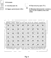
- Fig. 6 shows another embodiment in which a substrate 60 is provided, the substrate 60 being a metal substrate or it is a substrate coated with a metal layer.
- the substrate 60 is coated with an insulating layer 61; the insulating layer 61 is patterned by forming a matrix of holes defined by the outer circle of points 64.
- the SML is not shown to keep the figure simple, but it is formed under the OSL 62 and it is patterned as well with holes at the same position as the insulating layer 62 (also defined by the outer circle of points 64).
- the TCL is deposited on the rectangular area defined by the dashed line.
- the interconnections are made by laser and are defined by the black (full) circles 64.
- the OLED can be electrically connected to a power supply via an extension of the SML and an electrical connection to the substrate, or conductive layer on the substrate in case the substrate is non-conductive.
- the encapsulation is made before the interconnection step.
- Example 1 (not forming part of the present invention): Organic light emitting device comprising electrical interconnections
- a 100 mm x 100 mm glass substrate was provided.
- a 90 mm x 78 mm metal layer SML was deposited over the glass substrate.
- the metal layer is patterned forming parallel strips: wide strips (RA - region A) with the dimensions of 90 mm x 20 mm and narrow strips (RB - region B) with dimension of 90 mm x 3 mm; there is always a space of 1mm between the strips.
- the strips are formed in the following configuration: (RB) - 3x ((RA) - (RB)) ("-" indicates a lateral layer separation). This configuration is similar to the SML in Fig. 4 .
- An non-patterned 80 mm x 78 mm OSL comprising the following layers, was deposited over the SML as follows: 50 nm thick NPD layer doped with F4TCNQ; 10 nm thick non-doped NPD layer; 20 nm blue emitter host layer doped with a fluorescent emitter; 10 nm BPhen; 60 nm BPhen doped with Cs; and 20 nm Ag layer was deposited as TCL.
- the overlap between the OSL, (RA), and the TCL forms the bottom electrode.
- (RB) is the feed contact to the top electrode.
- the electrical interconnection was formed by applying laser pulses on the regions (RB); the laser was applied from the top-side (in other words, not through the substrate).
- the laser used in this example was a DPSS Nd:YAG laser operating at 1064 nm.
- the interconnecting points were fabricated over the 80 mm length of each of the regions (RB) (which length does overlap the OSL) with a linear density of 1 point / 250 ⁇ m.
- the regions extremities of the regions (RB) (which do not overlap the OSL) where connected to the negative pole of a voltage supply and the extremities of the regions (RA) were connected to the positive pole of the voltage supply.
- This device was formed with 3 light-emitting regions connected in parallel, all three regions worked with a high luminance and a high homogeneity of the emitting light intensity over the emitting surface.
- Example 2 (not forming part of the present invention): Organic light emitting device on a metal substrate and electrical interconnections
- Example 1 A 0,8 mm thick stainless steel plate with lateral dimensions of 100 mm x 100 mm, was provided as substrate.
- a 2,3 ⁇ m thick polyimide layer (PI2555 from HD microsystems) was deposited on the metal substrate by spin coating at 3500 rpm and heated at 180 °C for half an hour. The steps of Example 1) were repeated (expect for the first one: providing the glass substrate). The device worked as in Example 1), as expected.
- Example 3 (not forming part of the present invention): Organic light emitting device on a metal substrate and electrical interconnections
- a 0,8 mm thick stainless steel plate with lateral dimensions of 100 mm x 100 mm was provided as substrate.
- a 2,3 ⁇ m thick photodefineable polyimide layer (HD-8820 from HD microsystems) was deposited on the metal substrate by spin coating at 3500 rpm. The polyimide layer is heated at 120 °C for 3 minutes; the pattern is defined by exposing to a light pattern for 50 seconds, developed for 120 seconds and heated at 180 °C for half an hour.
- a 100 nm thick SML layer of Ag was deposited on the polyimide layer (RA) and on the exposed substrate areas (RB), as shown in Fig. 4 . In this case, the feed contact is provided by the substrate itself (the areas (RB)).
- the steps of depositing the OSL and the TCL were repeated as in Example 1).
- the electrical interconnection was formed by applying laser pulses on the regions (RB); the laser was applied from the top-side (in other words, not through the substrate).
- the laser used in this example was a pulsed Nd:YVO4 laser operating at 1064 nm.
- the interconnecting points were fabricated over the 80 mm length of each of the regions (RB) (which length does overlap the OSL) with a linear density of 1 point / 250 ⁇ m.
- Example 4 Organic light emitting device on a metal substrate and electrical interconnections
- Example 3 was repeated with the following modifications.
- the polyimide layer was patterned as in Fig. 5 .
- the SML was not deposited in contact with the metal substrate, it was patterned to only be deposited over the polyimide layer, as the in Fig. 5 .
- Example 5 Organic light emitting device with electrical interconnections
- a 0,8 mm thick stainless steel plate with lateral dimensions of 100 mm x 100 mm was provided as substrate.
- a 2,3 ⁇ m thick photo definable polyimide layer (HD-8820 from HD microsystems) was deposited on the metal substrate by spin coating.
- the polyimide layer is heated at 120 °C for 3 minutes; the pattern is defined by exposing to a light pattern for 50 seconds, developed for 120 seconds and heated at 180 °C for half an hour.
- the polyimide layer is patterned to expose the substrate as a matrix of holes. The spacing between row and columns of the matrix was 20 mm, and each hole had a diameter of 1 mm. A 100 nm thick SML layer of Ag was deposited on the polyimide layer.
- a frequency doubled Nd:YAG laser was used to remove the SML and the insulating layer in the holes, exposing the substrate.
- the photo definable polyimide layer or an additional photoresist could be used to pattern the SML, although it increases complexity.
- the electrical interconnection was formed by applying laser pulses on the center of each hole forming 3 adjacent interconnections; the laser was applied from the top-side (in other words, not through the substrate).
- the laser used in this example was a pulsed Nd:YAG laser operating at 1064 nm.
- the method resulted in a device depicted by Fig. 6 .
- the OLED showed a high homogeneity of the emitted light over the device's surface.
- Example 6 Encapsulated organic light emitting device with electrical interconnections
- the example 5 was repeated, however the device was encapsulated with a glass cover and step of making the electrical interconnections was done after the encapsulation, irradiating the laser through the glass cover.
- the advantage is that the interconnecting step could be done in air, whereas it has to be done under inert atmosphere for non-encapsulated samples, which are sensitive to oxygen, moisture, and dust.
- Example 7 Encapsulated organic light emitting device with electrical interconnections over glass
- Example 6 was repeated, with the following modification: A glass substrate comprising a relatively thick, non-patterned, metal layer of 500 nm (TML) was used in place of the metal substrate.
- TTL 500 nm
- Example 8 Organic light emitting device with maskless deposition
- a 0,8 mm thick stainless steel plate with lateral dimensions of 100 mm x 100 mm was provided as substrate.
- a 2,3 ⁇ m thick polyimide layer (PI2555 from HD microsystems) was deposited on the metal substrate by spin coating at 3500 rpm and heated at 180 °C for half an hour.
- a 100 nm thick SML layer of Ag was deposited on the polyimide layer.
- Example 1 The steps of depositing the OSL and the TCL were repeated as in Example 1), essentially unpatterned but with defining an area such that electrical connections from a power supply could be made to the electrodes.
- the electrical interconnection was formed by applying laser pulses on the center of each hole forming the interconnections; the laser was applied from the top-side (in other words, not through the substrate) using optical alignment (however it could be made without optical alignment).
- the interconnections were made 1 / mm in a matrix format.
- the OLED worked as expected with a very high homogeneity. With this highly simplified method it was possible to make a large area light emitting organic device without any mask or lithographic patterning step.
- the area covered by the TCL can extend over the area of the OSL providing an additional electrical contact to the conductor which supplies its current (e.g. to the metal substrate).
Landscapes
- Engineering & Computer Science (AREA)
- Manufacturing & Machinery (AREA)
- Physics & Mathematics (AREA)
- Electromagnetism (AREA)
- Optics & Photonics (AREA)
- Microelectronics & Electronic Packaging (AREA)
- Electroluminescent Light Sources (AREA)
Claims (7)
- Verfahren zum Herstellen einer top-emittierenden organischen lichtemittierenden Diode, wobei das Verfahren die folgenden Schritte in der folgenden Reihenfolge umfasst:- Bereitstellen eines Substrats, wobei das Substrat aus einem metallischen Material oder aus einem nicht-metallischem Material, das mit einer Metallschicht bedeckt ist, gebildet ist,- Bilden einer strukturierten isolierenden Schicht auf dem Substrat,- Bilden einer metallisierten Struktur, welche einen Abschnitt A und einen Abschnitt B umfasst, wobei der Abschnitt A über der isolierenden Schicht gebildet ist und eine Grundelektrode bereitstellt, und wobei der Abschnitt B mittels des metallischen Materials des Substrats oder mittels der Metallschicht auf dem nicht-metallischen Material des Substrats gebildet ist und einen Zuführungskontakt für eine Top-Elektrode bereitstellt,
wobei die Abschnitte A und B elektrisch voneinander isoliert sind,- Abscheiden einer organischen halbleitenden Schicht über der metallisierten Struktur,- Abscheiden einer transparenten leitfähigen Schicht über der organischen halbleitenden Schicht zum Bereitstellen einer Top-Elektrode und- Ausbilden eines elektrischen Kurzschlusses zwischen der Top-Elektrode und dem Zuführungskontakt in einem Verbindungsbereich, indem die Top-Elektrode mit dem Zuführungskontakt mittels Einstrahlen von Laserlicht durch die organische halbleitende Schicht in dem Verbindungsbereich elektrisch verbunden wird. - Verfahren nach Anspruch 1, wobei das Bilden der strukturierten isolierenden Schicht folgende Schritte umfasst:- Bilden einer isolierenden Schicht über dem Substrat und- Strukturieren der isolierenden Schicht.
- Verfahren nach Anspruch 2, wobei das Strukturieren der isolierenden Schicht eine Strukturierung der isolierenden Schicht mittels Laserablation umfasst.
- Verfahren nach einem der vorangehenden Ansprüche, wobei das Bilden der metallisierten Struktur folgende Schritte umfasst:- Abscheiden einer Metallschicht über dem Substrat und- Strukturieren der Metallschicht.
- Verfahren nach Anspruch 4, wobei das Strukturieren der Metallschicht ein Strukturieren der Metallschicht mittels Laserablation umfasst.
- Verfahren nach einem der vorangehenden Ansprüche, wobei das Bilden der metallisierten Struktur folgende Schritte umfasst:- Abscheiden einer Schicht aus einem Photolack über dem Substrat,- Abscheiden einer Metallschicht über der Photolackschicht und- Strukturieren der Metallschicht mittels teilweisem Entfernen des Photolacks.
- Verfahren nach einem der vorangehenden Ansprüche, weiter umfassend:- Verkapseln der organischen lichtemittierenden Diode und- Bilden eines elektrischen Kurzschlusses zwischen der Top-Elektrode und dem Zuführungskontakt mittels Einstrahlen von Laserlicht vor oder nach dem Verkapseln der organischen lichtemittierenden Diode.
Priority Applications (4)
| Application Number | Priority Date | Filing Date | Title |
|---|---|---|---|
| EP09015017.8A EP2333859B1 (de) | 2009-12-03 | 2009-12-03 | Verfahren zum Bilden einer organischen lichtemittierenden Diode |
| CN201010579211.7A CN102136549B (zh) | 2009-12-03 | 2010-12-03 | 用于在有机光电子器件中形成电互连的方法、用于制造有机光电子器件的方法以及有机发光器件 |
| JP2010270603A JP2011124231A (ja) | 2009-12-03 | 2010-12-03 | 有機光学電子装置における電気的相互接続部を形成する方法、有機光学電子装置を製造する方法、および、有機発光装置 |
| KR1020100122581A KR101742114B1 (ko) | 2009-12-03 | 2010-12-03 | 유기 광-전자 디바이스에 전기 상호접속부를 형성하기 위한 방법, 유기 광-전자 디바이스를 형성하기 위한 방법, 및 유기 발광 디바이스 |
Applications Claiming Priority (1)
| Application Number | Priority Date | Filing Date | Title |
|---|---|---|---|
| EP09015017.8A EP2333859B1 (de) | 2009-12-03 | 2009-12-03 | Verfahren zum Bilden einer organischen lichtemittierenden Diode |
Publications (2)
| Publication Number | Publication Date |
|---|---|
| EP2333859A1 EP2333859A1 (de) | 2011-06-15 |
| EP2333859B1 true EP2333859B1 (de) | 2017-09-13 |
Family
ID=42111106
Family Applications (1)
| Application Number | Title | Priority Date | Filing Date |
|---|---|---|---|
| EP09015017.8A Active EP2333859B1 (de) | 2009-12-03 | 2009-12-03 | Verfahren zum Bilden einer organischen lichtemittierenden Diode |
Country Status (1)
| Country | Link |
|---|---|
| EP (1) | EP2333859B1 (de) |
Cited By (1)
| Publication number | Priority date | Publication date | Assignee | Title |
|---|---|---|---|---|
| US10777693B2 (en) | 2013-12-17 | 2020-09-15 | Oxford University Innovation Limited | Photovoltaic device comprising a metal halide perovskite and a passivating agent |
Families Citing this family (7)
| Publication number | Priority date | Publication date | Assignee | Title |
|---|---|---|---|---|
| TWI565119B (zh) | 2011-05-27 | 2017-01-01 | 半導體能源研究所股份有限公司 | 發光裝置的製造方法及發光裝置 |
| KR102244374B1 (ko) | 2013-08-09 | 2021-04-26 | 가부시키가이샤 한도오따이 에네루기 켄큐쇼 | 발광 소자, 디스플레이 모듈, 조명 모듈, 발광 장치, 표시 장치, 전자 기기, 및 조명 장치 |
| TWI790559B (zh) | 2013-08-09 | 2023-01-21 | 日商半導體能源研究所股份有限公司 | 發光元件、顯示模組、照明模組、發光裝置、顯示裝置、電子裝置、及照明裝置 |
| US10153449B2 (en) | 2014-10-16 | 2018-12-11 | Semiconductor Energy Laboratory Co., Ltd. | Light-emitting element, light-emitting device, electronic device, and lighting device |
| DE102017200896A1 (de) * | 2017-01-20 | 2018-07-26 | Opvius Gmbh | Verfahren zur Herstellung eines organischen Halbleiterbauteils und organisches Halbleiterbauteil |
| DE102017101390A1 (de) * | 2017-01-25 | 2018-07-26 | Osram Oled Gmbh | Organisches Licht emittierendes Bauelement und Verfahren zur Herstellung eines organischen Licht emittierenden Bauelements |
| EP3620894A1 (de) * | 2018-09-04 | 2020-03-11 | Robert Bosch GmbH | Haptische schnittstelle, strukturierte schichtstruktur für eine haptische schnittstelle und verfahren zur herstellung davon |
Citations (1)
| Publication number | Priority date | Publication date | Assignee | Title |
|---|---|---|---|---|
| WO2007004115A2 (en) * | 2005-06-30 | 2007-01-11 | Koninklijke Philips Electronics N.V. | Organic electronic device and method for manufacture thereof |
Family Cites Families (4)
| Publication number | Priority date | Publication date | Assignee | Title |
|---|---|---|---|---|
| US6995035B2 (en) | 2003-06-16 | 2006-02-07 | Eastman Kodak Company | Method of making a top-emitting OLED device having improved power distribution |
| US7122489B2 (en) * | 2004-05-12 | 2006-10-17 | Matsushita Electric Industrial Co., Ltd. | Manufacturing method of composite sheet material using ultrafast laser pulses |
| US7733441B2 (en) * | 2004-06-03 | 2010-06-08 | Semiconductor Energy Labortory Co., Ltd. | Organic electroluminescent lighting system provided with an insulating layer containing fluorescent material |
| JP2009266451A (ja) | 2008-04-23 | 2009-11-12 | Sony Corp | 表示装置の製造方法および転写基板 |
-
2009
- 2009-12-03 EP EP09015017.8A patent/EP2333859B1/de active Active
Patent Citations (1)
| Publication number | Priority date | Publication date | Assignee | Title |
|---|---|---|---|---|
| WO2007004115A2 (en) * | 2005-06-30 | 2007-01-11 | Koninklijke Philips Electronics N.V. | Organic electronic device and method for manufacture thereof |
Cited By (3)
| Publication number | Priority date | Publication date | Assignee | Title |
|---|---|---|---|---|
| US10777693B2 (en) | 2013-12-17 | 2020-09-15 | Oxford University Innovation Limited | Photovoltaic device comprising a metal halide perovskite and a passivating agent |
| US11799039B2 (en) | 2013-12-17 | 2023-10-24 | Oxford University Innovation Limited | Photovoltaic device comprising a metal halide perovskite and a passivating agent |
| US12288825B2 (en) | 2013-12-17 | 2025-04-29 | Oxford Photovoltaics Limited | Photovoltaic device comprising a metal halide perovskite and a passivating agent |
Also Published As
| Publication number | Publication date |
|---|---|
| EP2333859A1 (de) | 2011-06-15 |
Similar Documents
| Publication | Publication Date | Title |
|---|---|---|
| EP2333859B1 (de) | Verfahren zum Bilden einer organischen lichtemittierenden Diode | |
| CN102549797B (zh) | 单片并联互连结构 | |
| CN102144314B (zh) | 用于制造发射辐射的有机器件的方法以及发射辐射的有机器件 | |
| EP2355199B1 (de) | Verfahren zur Herstellung einer organischen lichtemittierenden Vorrichtung | |
| US7563707B2 (en) | Laser process for reliable and low-resistance electrical contacts | |
| KR101742114B1 (ko) | 유기 광-전자 디바이스에 전기 상호접속부를 형성하기 위한 방법, 유기 광-전자 디바이스를 형성하기 위한 방법, 및 유기 발광 디바이스 | |
| KR101315086B1 (ko) | 유기 전자 장치 및 그 제조 방법 | |
| JP2013516735A (ja) | 有機発光ダイオード装置のマスクレス製造の方法 | |
| US6719916B2 (en) | Multilayer microstructures and laser based method for precision and reduced damage patterning of such structures | |
| CN101213682B (zh) | 用于在有机功能设备中形成电极层图案的方法 | |
| US9379349B2 (en) | OLED device with spatially isolated light-emitting areas | |
| US8816335B2 (en) | Method for creating serially-connected OLED devices | |
| US20040149986A1 (en) | Multilayer microstructures and laser based method for precision and reduced damage patterning of such structures | |
| JP5460291B2 (ja) | 有機発光装置の製造方法および有機発光装置 | |
| KR20080100058A (ko) | 발광 다이오드의 제조 방법 | |
| EP2148370A1 (de) | Struktur für elektrooptische Vorrichtungen | |
| CA2381643C (en) | Multilayer microstructures and laser based method for precision and reduced damage patterning of such structures |
Legal Events
| Date | Code | Title | Description |
|---|---|---|---|
| PUAI | Public reference made under article 153(3) epc to a published international application that has entered the european phase |
Free format text: ORIGINAL CODE: 0009012 |
|
| AK | Designated contracting states |
Kind code of ref document: A1 Designated state(s): AT BE BG CH CY CZ DE DK EE ES FI FR GB GR HR HU IE IS IT LI LT LU LV MC MK MT NL NO PL PT RO SE SI SK SM TR |
|
| AX | Request for extension of the european patent |
Extension state: AL BA RS |
|
| 17P | Request for examination filed |
Effective date: 20111212 |
|
| 17Q | First examination report despatched |
Effective date: 20141017 |
|
| REG | Reference to a national code |
Ref country code: DE Ref legal event code: R079 Ref document number: 602009048286 Country of ref document: DE Free format text: PREVIOUS MAIN CLASS: H01L0051000000 Ipc: H01L0051560000 |
|
| GRAP | Despatch of communication of intention to grant a patent |
Free format text: ORIGINAL CODE: EPIDOSNIGR1 |
|
| RIC1 | Information provided on ipc code assigned before grant |
Ipc: H01L 51/56 20060101AFI20170405BHEP |
|
| INTG | Intention to grant announced |
Effective date: 20170420 |
|
| GRAS | Grant fee paid |
Free format text: ORIGINAL CODE: EPIDOSNIGR3 |
|
| GRAA | (expected) grant |
Free format text: ORIGINAL CODE: 0009210 |
|
| AK | Designated contracting states |
Kind code of ref document: B1 Designated state(s): AT BE BG CH CY CZ DE DK EE ES FI FR GB GR HR HU IE IS IT LI LT LU LV MC MK MT NL NO PL PT RO SE SI SK SM TR |
|
| RAP1 | Party data changed (applicant data changed or rights of an application transferred) |
Owner name: NOVALED GMBH |
|
| REG | Reference to a national code |
Ref country code: GB Ref legal event code: FG4D |
|
| RIN1 | Information on inventor provided before grant (corrected) |
Inventor name: BLOCHWITZ-NIMOTH, JAN DR. Inventor name: JOBERT, PIERRE PAUL Inventor name: LESSMANN, RUDOLF DR. |
|
| REG | Reference to a national code |
Ref country code: CH Ref legal event code: EP |
|
| REG | Reference to a national code |
Ref country code: IE Ref legal event code: FG4D |
|
| REG | Reference to a national code |
Ref country code: FR Ref legal event code: PLFP Year of fee payment: 9 |
|
| REG | Reference to a national code |
Ref country code: AT Ref legal event code: REF Ref document number: 928947 Country of ref document: AT Kind code of ref document: T Effective date: 20171015 |
|
| REG | Reference to a national code |
Ref country code: DE Ref legal event code: R096 Ref document number: 602009048286 Country of ref document: DE |
|
| REG | Reference to a national code |
Ref country code: NL Ref legal event code: MP Effective date: 20170913 |
|
| REG | Reference to a national code |
Ref country code: LT Ref legal event code: MG4D |
|
| PG25 | Lapsed in a contracting state [announced via postgrant information from national office to epo] |
Ref country code: NO Free format text: LAPSE BECAUSE OF FAILURE TO SUBMIT A TRANSLATION OF THE DESCRIPTION OR TO PAY THE FEE WITHIN THE PRESCRIBED TIME-LIMIT Effective date: 20171213 Ref country code: SE Free format text: LAPSE BECAUSE OF FAILURE TO SUBMIT A TRANSLATION OF THE DESCRIPTION OR TO PAY THE FEE WITHIN THE PRESCRIBED TIME-LIMIT Effective date: 20170913 Ref country code: LT Free format text: LAPSE BECAUSE OF FAILURE TO SUBMIT A TRANSLATION OF THE DESCRIPTION OR TO PAY THE FEE WITHIN THE PRESCRIBED TIME-LIMIT Effective date: 20170913 Ref country code: FI Free format text: LAPSE BECAUSE OF FAILURE TO SUBMIT A TRANSLATION OF THE DESCRIPTION OR TO PAY THE FEE WITHIN THE PRESCRIBED TIME-LIMIT Effective date: 20170913 Ref country code: HR Free format text: LAPSE BECAUSE OF FAILURE TO SUBMIT A TRANSLATION OF THE DESCRIPTION OR TO PAY THE FEE WITHIN THE PRESCRIBED TIME-LIMIT Effective date: 20170913 |
|
| REG | Reference to a national code |
Ref country code: AT Ref legal event code: MK05 Ref document number: 928947 Country of ref document: AT Kind code of ref document: T Effective date: 20170913 |
|
| PG25 | Lapsed in a contracting state [announced via postgrant information from national office to epo] |
Ref country code: BG Free format text: LAPSE BECAUSE OF FAILURE TO SUBMIT A TRANSLATION OF THE DESCRIPTION OR TO PAY THE FEE WITHIN THE PRESCRIBED TIME-LIMIT Effective date: 20171213 Ref country code: GR Free format text: LAPSE BECAUSE OF FAILURE TO SUBMIT A TRANSLATION OF THE DESCRIPTION OR TO PAY THE FEE WITHIN THE PRESCRIBED TIME-LIMIT Effective date: 20171214 Ref country code: ES Free format text: LAPSE BECAUSE OF FAILURE TO SUBMIT A TRANSLATION OF THE DESCRIPTION OR TO PAY THE FEE WITHIN THE PRESCRIBED TIME-LIMIT Effective date: 20170913 Ref country code: LV Free format text: LAPSE BECAUSE OF FAILURE TO SUBMIT A TRANSLATION OF THE DESCRIPTION OR TO PAY THE FEE WITHIN THE PRESCRIBED TIME-LIMIT Effective date: 20170913 |
|
| PG25 | Lapsed in a contracting state [announced via postgrant information from national office to epo] |
Ref country code: NL Free format text: LAPSE BECAUSE OF FAILURE TO SUBMIT A TRANSLATION OF THE DESCRIPTION OR TO PAY THE FEE WITHIN THE PRESCRIBED TIME-LIMIT Effective date: 20170913 |
|
| PG25 | Lapsed in a contracting state [announced via postgrant information from national office to epo] |
Ref country code: PL Free format text: LAPSE BECAUSE OF FAILURE TO SUBMIT A TRANSLATION OF THE DESCRIPTION OR TO PAY THE FEE WITHIN THE PRESCRIBED TIME-LIMIT Effective date: 20170913 Ref country code: CZ Free format text: LAPSE BECAUSE OF FAILURE TO SUBMIT A TRANSLATION OF THE DESCRIPTION OR TO PAY THE FEE WITHIN THE PRESCRIBED TIME-LIMIT Effective date: 20170913 Ref country code: RO Free format text: LAPSE BECAUSE OF FAILURE TO SUBMIT A TRANSLATION OF THE DESCRIPTION OR TO PAY THE FEE WITHIN THE PRESCRIBED TIME-LIMIT Effective date: 20170913 |
|
| PG25 | Lapsed in a contracting state [announced via postgrant information from national office to epo] |
Ref country code: AT Free format text: LAPSE BECAUSE OF FAILURE TO SUBMIT A TRANSLATION OF THE DESCRIPTION OR TO PAY THE FEE WITHIN THE PRESCRIBED TIME-LIMIT Effective date: 20170913 Ref country code: EE Free format text: LAPSE BECAUSE OF FAILURE TO SUBMIT A TRANSLATION OF THE DESCRIPTION OR TO PAY THE FEE WITHIN THE PRESCRIBED TIME-LIMIT Effective date: 20170913 Ref country code: SM Free format text: LAPSE BECAUSE OF FAILURE TO SUBMIT A TRANSLATION OF THE DESCRIPTION OR TO PAY THE FEE WITHIN THE PRESCRIBED TIME-LIMIT Effective date: 20170913 Ref country code: IT Free format text: LAPSE BECAUSE OF FAILURE TO SUBMIT A TRANSLATION OF THE DESCRIPTION OR TO PAY THE FEE WITHIN THE PRESCRIBED TIME-LIMIT Effective date: 20170913 Ref country code: SK Free format text: LAPSE BECAUSE OF FAILURE TO SUBMIT A TRANSLATION OF THE DESCRIPTION OR TO PAY THE FEE WITHIN THE PRESCRIBED TIME-LIMIT Effective date: 20170913 Ref country code: IS Free format text: LAPSE BECAUSE OF FAILURE TO SUBMIT A TRANSLATION OF THE DESCRIPTION OR TO PAY THE FEE WITHIN THE PRESCRIBED TIME-LIMIT Effective date: 20180113 |
|
| REG | Reference to a national code |
Ref country code: DE Ref legal event code: R097 Ref document number: 602009048286 Country of ref document: DE |
|
| PLBE | No opposition filed within time limit |
Free format text: ORIGINAL CODE: 0009261 |
|
| STAA | Information on the status of an ep patent application or granted ep patent |
Free format text: STATUS: NO OPPOSITION FILED WITHIN TIME LIMIT |
|
| PG25 | Lapsed in a contracting state [announced via postgrant information from national office to epo] |
Ref country code: DK Free format text: LAPSE BECAUSE OF FAILURE TO SUBMIT A TRANSLATION OF THE DESCRIPTION OR TO PAY THE FEE WITHIN THE PRESCRIBED TIME-LIMIT Effective date: 20170913 |
|
| REG | Reference to a national code |
Ref country code: CH Ref legal event code: PL |
|
| 26N | No opposition filed |
Effective date: 20180614 |
|
| REG | Reference to a national code |
Ref country code: IE Ref legal event code: MM4A |
|
| PG25 | Lapsed in a contracting state [announced via postgrant information from national office to epo] |
Ref country code: LU Free format text: LAPSE BECAUSE OF NON-PAYMENT OF DUE FEES Effective date: 20171203 Ref country code: MT Free format text: LAPSE BECAUSE OF NON-PAYMENT OF DUE FEES Effective date: 20171203 |
|
| REG | Reference to a national code |
Ref country code: FR Ref legal event code: PLFP Year of fee payment: 10 |
|
| REG | Reference to a national code |
Ref country code: BE Ref legal event code: MM Effective date: 20171231 |
|
| PG25 | Lapsed in a contracting state [announced via postgrant information from national office to epo] |
Ref country code: IE Free format text: LAPSE BECAUSE OF NON-PAYMENT OF DUE FEES Effective date: 20171203 |
|
| PG25 | Lapsed in a contracting state [announced via postgrant information from national office to epo] |
Ref country code: CH Free format text: LAPSE BECAUSE OF NON-PAYMENT OF DUE FEES Effective date: 20171231 Ref country code: SI Free format text: LAPSE BECAUSE OF FAILURE TO SUBMIT A TRANSLATION OF THE DESCRIPTION OR TO PAY THE FEE WITHIN THE PRESCRIBED TIME-LIMIT Effective date: 20170913 Ref country code: BE Free format text: LAPSE BECAUSE OF NON-PAYMENT OF DUE FEES Effective date: 20171231 Ref country code: LI Free format text: LAPSE BECAUSE OF NON-PAYMENT OF DUE FEES Effective date: 20171231 |
|
| PG25 | Lapsed in a contracting state [announced via postgrant information from national office to epo] |
Ref country code: HU Free format text: LAPSE BECAUSE OF FAILURE TO SUBMIT A TRANSLATION OF THE DESCRIPTION OR TO PAY THE FEE WITHIN THE PRESCRIBED TIME-LIMIT; INVALID AB INITIO Effective date: 20091203 Ref country code: MC Free format text: LAPSE BECAUSE OF FAILURE TO SUBMIT A TRANSLATION OF THE DESCRIPTION OR TO PAY THE FEE WITHIN THE PRESCRIBED TIME-LIMIT Effective date: 20170913 |
|
| PG25 | Lapsed in a contracting state [announced via postgrant information from national office to epo] |
Ref country code: CY Free format text: LAPSE BECAUSE OF NON-PAYMENT OF DUE FEES Effective date: 20170913 |
|
| PG25 | Lapsed in a contracting state [announced via postgrant information from national office to epo] |
Ref country code: MK Free format text: LAPSE BECAUSE OF FAILURE TO SUBMIT A TRANSLATION OF THE DESCRIPTION OR TO PAY THE FEE WITHIN THE PRESCRIBED TIME-LIMIT Effective date: 20170913 |
|
| PG25 | Lapsed in a contracting state [announced via postgrant information from national office to epo] |
Ref country code: TR Free format text: LAPSE BECAUSE OF FAILURE TO SUBMIT A TRANSLATION OF THE DESCRIPTION OR TO PAY THE FEE WITHIN THE PRESCRIBED TIME-LIMIT Effective date: 20170913 |
|
| PG25 | Lapsed in a contracting state [announced via postgrant information from national office to epo] |
Ref country code: PT Free format text: LAPSE BECAUSE OF FAILURE TO SUBMIT A TRANSLATION OF THE DESCRIPTION OR TO PAY THE FEE WITHIN THE PRESCRIBED TIME-LIMIT Effective date: 20170913 |
|
| REG | Reference to a national code |
Ref country code: DE Ref legal event code: R079 Ref document number: 602009048286 Country of ref document: DE Free format text: PREVIOUS MAIN CLASS: H01L0051560000 Ipc: H10K0050000000 |
|
| P01 | Opt-out of the competence of the unified patent court (upc) registered |
Effective date: 20230515 |
|
| PGFP | Annual fee paid to national office [announced via postgrant information from national office to epo] |
Ref country code: DE Payment date: 20241001 Year of fee payment: 16 |
|
| PGFP | Annual fee paid to national office [announced via postgrant information from national office to epo] |
Ref country code: GB Payment date: 20241001 Year of fee payment: 16 |
|
| PGFP | Annual fee paid to national office [announced via postgrant information from national office to epo] |
Ref country code: FR Payment date: 20241001 Year of fee payment: 16 |