EP2325899A1 - Semiconductor device - Google Patents
Semiconductor device Download PDFInfo
- Publication number
- EP2325899A1 EP2325899A1 EP09810080A EP09810080A EP2325899A1 EP 2325899 A1 EP2325899 A1 EP 2325899A1 EP 09810080 A EP09810080 A EP 09810080A EP 09810080 A EP09810080 A EP 09810080A EP 2325899 A1 EP2325899 A1 EP 2325899A1
- Authority
- EP
- European Patent Office
- Prior art keywords
- layer
- light emitting
- quantum well
- semiconductor device
- composition
- Prior art date
- Legal status (The legal status is an assumption and is not a legal conclusion. Google has not performed a legal analysis and makes no representation as to the accuracy of the status listed.)
- Withdrawn
Links
Images


Classifications
-
- H—ELECTRICITY
- H10—SEMICONDUCTOR DEVICES; ELECTRIC SOLID-STATE DEVICES NOT OTHERWISE PROVIDED FOR
- H10H—INORGANIC LIGHT-EMITTING SEMICONDUCTOR DEVICES HAVING POTENTIAL BARRIERS
- H10H20/00—Individual inorganic light-emitting semiconductor devices having potential barriers, e.g. light-emitting diodes [LED]
- H10H20/80—Constructional details
- H10H20/81—Bodies
- H10H20/822—Materials of the light-emitting regions
- H10H20/824—Materials of the light-emitting regions comprising only Group III-V materials, e.g. GaP
- H10H20/825—Materials of the light-emitting regions comprising only Group III-V materials, e.g. GaP containing nitrogen, e.g. GaN
-
- H—ELECTRICITY
- H10—SEMICONDUCTOR DEVICES; ELECTRIC SOLID-STATE DEVICES NOT OTHERWISE PROVIDED FOR
- H10H—INORGANIC LIGHT-EMITTING SEMICONDUCTOR DEVICES HAVING POTENTIAL BARRIERS
- H10H20/00—Individual inorganic light-emitting semiconductor devices having potential barriers, e.g. light-emitting diodes [LED]
- H10H20/80—Constructional details
- H10H20/81—Bodies
- H10H20/811—Bodies having quantum effect structures or superlattices, e.g. tunnel junctions
-
- H—ELECTRICITY
- H10—SEMICONDUCTOR DEVICES; ELECTRIC SOLID-STATE DEVICES NOT OTHERWISE PROVIDED FOR
- H10H—INORGANIC LIGHT-EMITTING SEMICONDUCTOR DEVICES HAVING POTENTIAL BARRIERS
- H10H20/00—Individual inorganic light-emitting semiconductor devices having potential barriers, e.g. light-emitting diodes [LED]
- H10H20/80—Constructional details
- H10H20/81—Bodies
- H10H20/811—Bodies having quantum effect structures or superlattices, e.g. tunnel junctions
- H10H20/812—Bodies having quantum effect structures or superlattices, e.g. tunnel junctions within the light-emitting regions, e.g. having quantum confinement structures
Definitions
- the present invention relates to a semiconductor device.
- the present invention aims to provide a semiconductor device capable of obtaining a light emitting diode with high light emitting efficiency.
- a semiconductor device comprises an underlying layer; and a light emitting layer which is formed on the underlying layer and in which a barrier layer made of InAlGaN and a quantum well layer made of InGaN are alternately stacked.
- the present invention it is possible to provide a semiconductor device capable of obtaining a light emitting diode with high light emitting efficiency.
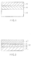
- FIG. 1 is cross sectional view schematically showing a basic structure of a semiconductor device (light emitting diode) according to a first embodiment of the present invention.
- the semiconductor device shown in FIG. 1 is configured with a substrate 10, an underlying layer 20 formed on the substrate 10, and a light emitting layer 30 formed on the underlying layer 20.
- the barrier layer 31 is made of InAlGaN (generally expressed as In x Al y Ga 1-x-y N (0 ⁇ x ⁇ 1, 0 ⁇ y ⁇ 1)) and has a thickness of 12.5 nm. Specifically, the barrier layer 31 is made of In 0.02 Al 0.33 Ga 0.65 N.
- the intermediate layer 32 is made of InGaN (generally expressed as In x Ga 1-x N (0 ⁇ x ⁇ 1)) and has a thickness of 0.5 nm. Specifically, the intermediate layer 32 is made of In 0.02 Ga 0.98 N.
- the quantum well layer 33 is made of InGaN (generally expressed as In x Ga 1-x N (0 ⁇ x ⁇ 1)) and has a thickness of 2.5 nm. Specifically, the quantum well layer 33 is made of In 0.15 Ga 0.85 N.
- the intermediate layer 34 is made of InGaN (generally expressed as In x Ga 1-x N (0 ⁇ x ⁇ 1)) and has a thickness of 0.5 nm. Specifically, the intermediate layer 34 is made of In 0.02 Ga 0.98 N.
- the barrier layer 35 is made of InAlGaN (generally expressed as In x Al y Ga 1-x-y N (0 ⁇ x ⁇ 1, 0 ⁇ y ⁇ 1)) and has a thickness of 11.5 nm. Specifically, the barrier layer 35 is made of In 0.02 Al 0.33 Ga 0.65 N.
- the stack structure in FIG. 2 is formed for 5 cycles. Then, an InAlGaN (generally expressed as In x Al y Ga 1-x-y N (0 ⁇ x ⁇ 1, 0 ⁇ y ⁇ 1)) layer having a thickness of 15 nm is formed as a cap layer at the uppermost layer. Specifically, the cap layer is made of In 0.02 Al 0.33 Ga 0.65 N.
- InAlGaN generally expressed as In x Al y Ga 1-x-y N (0 ⁇ x ⁇ 1, 0 ⁇ y ⁇ 1)
- the cap layer is made of In 0.02 Al 0.33 Ga 0.65 N.
- the aforementioned structure is formed by epitaxial growth of the underlying layer 20 and the light emitting layer 30 on the (0001) surface (that is, C surface) of the sapphire substrate 10.
- a metal organic chemical vapor deposition (MOCVD) method, molecular beam epitaxy (MBE) method or the like can be employed for the epitaxial growth method.
- the semiconductor device according to the present embodiment described above can obtain a light emitting diode with high light emitting efficiency and high luminance. The reasons therefor will be described below.
- FIG. 3 is a diagram showing a relationship between a lattice constant and a bandgap in a compound semiconductor.
- the lattice constant is larger in InGaN than in GaN, and the lattice constant of InGaN increases as an In composition of InGaN increases. Therefore, when the InGaN layer having a high In composition is grown on the GaN layer as in the quantum well layer, a compressive strain occurs in the planar direction (a-axis direction) and a tensile strain occurs in the growth direction (c-axis direction).
- the InGaN layer having a low In composition or the InAlGaN layer having a low In composition is provided as the barrier layer, thereby alleviating the compressive strain in the planar direction (a-axis direction).
- the tensile strain in the growth direction (c-axis direction) cannot be largely alleviated.
- the tensile strain in the c-axis direction is large, a piezoelectric field due to piezoelectric polarization is made larger.
- a possibility of recombination between electron and hole is lowered and the light emitting efficiency is lowered.
- the piezoelectric field due to the tensile strain in the c-axis direction increases along with an increase in In composition.
- the injected current density dependency of the quantum efficiency shows that the decrease of the quantum efficiency in a high injected current density region is remarkable, and it is not suitable for a light emitting diode used at the high injected current density.
- the In composition of the quantum well layer needs to be increased for elongating a light emitting wavelength (for reducing a bandgap). From the above, when the InGaN layer having a low In composition is employed as the barrier layer, it is difficult to elongate the light emitting wavelength without largely reducing the light emitting efficiency.
- the InAlGaN layer having a low In composition when employed as the barrier layer, the tensile strain in the growth direction (c-axis direction) can be largely alleviated.
- the InAlGaN layer is employed as the barrier layer, thereby elongating the light emitting wavelength without largely reducing the light emitting efficiency. Since the piezoelectric field can be reduced in the present embodiment, it is possible to prevent the decrease of the quantum efficiency in a high injected current density region, and the light emitting diode with high injected current density and high efficiency can be provided.
- InAlGaN as a barrier layer enables band gap energy of the barrier layer to increase, and overflow of carriers, particularly electrons, can be prevented.
- it is suitable for the light emitting diode used at the high injected current density. For example, it is possible to obtain a high power light emitting diode having current density of 100 A/cm 2 or more.
- the light emitting wavelength can be elongated more when the InAlGaN layer is employed as the barrier layer than when the InGaN layer is employed as the barrier layer.
- the light emitting wavelength can be elongated without largely reducing the light emitting efficiency. That is, when the light emitting diode having the same light emitting wavelength is manufactured, the In composition of the quantum well layer can be reduced in this embodiment. The description thereof will be made below. Originally, if the In composition of the InGaN quantum well layer is the same, the light emitting wavelength should not change.
- the InAlGaN layer is employed as the barrier layer so that the light emitting wavelength can be elongate, which may be based on the following reasons.
- a difference in bandgap and a difference in lattice constant between AlN and InN are larger than those between GaN and InN.
- a thermodynamic composition variation easily occurs.
- the InGaN layer having a high In composition is locally formed so that the light emitting wavelength can be elongated. Since the In composition of the quantum well layer can be reduced, the thermodynamic composition variation is prevented, and a thermodynamically stable crystal can be obtained. Thus, a semiconductor device with high reliability can be provided.
- the In composition of the quantum well layer can be reduced, it is possible to increase the thickness of the quantum well layer, and the current density per one quantum well layer can be reduced.
- the intermediate layer 32 is provided between the barrier layer 31 and the quantum well layer 33 and the intermediate layer 34 is provided between the barrier layer 35 and the quantum well layer 33 as shown in FIG. 2 .
- an intermediate layer is interposed between the barrier layer and the quantum well layer so that a lattice mismatch between the barrier layer and the quantum well layer can be restricted. Consequently, it is possible to restrict the occurrence of phase separation or defect and to improve the light emitting efficiency of the light emitting layer. This will be described below.
- the difference in lattice constant between AlN and InN is large.
- the Al composition of the InAlGaN barrier layer is reasonably high and the In composition of the InGaN quantum well layer is reasonably high.
- the InGaN intermediate layer having a low In composition is interposed between the barrier layer and the quantum well layer as long as it does not affect the band structure.
- the Ga composition is much higher than the In composition and GaN is dominant.
- GaN has an intermediate lattice constant between the AlN lattice constant and the InN lattice constant. Therefore, the InGaN intermediate layer is interposed between the InAlGaN barrier layer and the InGaN quantum well layer, thereby restricting the drastic lattice mismatch between the barrier layer and the quantum well layer. As a result, the occurrence of phase separation or defect can be restricted, thereby improving the light emitting efficiency.
- FIG. 5 is a diagram showing a measurement result of a semiconductor device (light emitting diode) according to a first comparative example of the present embodiment.
- the In composition of the quantum well layer is as high as 0.35 for making the barrier layer of InGaN and for elongating the light emitting wavelength.
- the light emitting intensity is more largely lowered in the comparative example than in the present embodiment.
- the comparative example it is assumed that since the In composition of the quantum well layer is high for achieving an elongated wavelength, the light emitting efficiency is largely lowered from the aforementioned reasons.
- FIG. 6 is a diagram showing a measurement result of a semiconductor device (light emitting diode) according to a second comparative example of the present embodiment.
- the barrier layer and the quantum well layer are stacked without providing the intermediate layer.
- the light emitting intensity is more largely lowered in the comparative example than in the present embodiment.
- the comparative example it is assumed that since the barrier layer and the quantum well layer are directly stacked without the intermediate layer, the light emitting efficiency is largely lowered from the aforementioned reasons.
- the Al composition of the barrier layer is preferably in the range of 0.2 to 0.4 and the In composition of the barrier layer is preferably in the range of 0.01 to 0.05.
- the thickness of the barrier layer is preferably in the range of 4 to 20 nm.
- the intermediate layer preferably has an In composition equal to or higher than that of the barrier layer.
- the In composition of the intermediate layer is preferably in the range of 0.01 to 0.05 similarly as the In composition of the barrier layer. In this manner, the drastic lattice mismatch can be restricted, thereby effectively restricting the occurrence of phase separation or defect.
- the In composition of the quantum well layer is preferably in the range of 0.1 to 0.3.
- the In composition of the quantum well layer is set to be higher than 0.3, an influence of the piezoelectric field is noticeable and the light emitting efficiency can be largely lowered. It is preferable to set the In composition of the quantum well layer at 0.3 or less and to adjust the Al composition of the barrier layer for controlling the light emitting wavelength. Furthermore, the thickness of the intermediate layer is preferably in the range of 0.5 to 1.5 nm.
- FIG. 7 is a cross sectional view schematically showing a structure of the semiconductor device (light emitting diode) according to the present embodiment.
- a sapphire substrate is employed for the substrate 10, and the upper surface (device forming surface) of the sapphire substrate 10 is the (0001) surface of sapphire crystal, that is, the C surface.
- An n-type GaN contact layer 21, an n-type GaN guide layer 22, the light emitting layer 30 having a multi quantum well structure, a p-type AlGaN overflow preventing layer 41, a p-type GaN layer 42 and a p-type GaN contact layer 43 are stacked on the upper surface (C surface) of the sapphire substrate 10.
- an n-side electrode 50 made of Ti/Pt/Au is formed on the exposed surface of the n-type GaN contact layer 21.
- a p-side electrode 60 made of Ni/Au is formed on the surface of the p-type GaN contact layer 43.
- the structure of the light emitting layer 30 is similar to the structure explained in the first embodiment.
- the overflow preventing layer is effective in the high power light emitting diode having the current density of, for example, about 100 A/cm 2 or more.
- the overflow preventing layer has the Al composition higher than that of the barrier layer.
- Each layer of the present semiconductor device is formed by the metal organic chemical vapor deposition (MOCVD) method.
- the materials therefor may employ trimethyl gallium (TMG), trimethyl aluminum (TMA), trimethyl indium (TMI) and bis (cyclopentadienyl) magnesium) (Cp2Mg).
- the gas material may employ ammonia (NH 3 ) and silane (SiH 4 ).
- the carrier gas may employ hydrogen and nitrogen.
- the sapphire substrate processed by organic cleaning and acid cleansing is introduced into a reaction chamber of the MOCVD apparatus and is put on a susceptor to be heated by high frequency.
- the sapphire substrate is raised in its temperature to 1100°C for 12 minutes under a nitrogen/hydrogen atmosphere at a normal pressure.
- gas phase etching is performed on the substrate surface to remove a native oxide film on the substrate surface.
- nitrogen/hydrogen is employed as a carrier gas to supply ammonia at a flow rate of 6 L/minute, TMG at a flow rate of 50 cc/minute and SiH 4 at a flow rate of 10 cc/minute, for 60 minutes, thereby forming the n-type GaN contact layer 21.
- the temperature is lowered to 1060°C and SiH 4 is lowered in its flow rate to 3 cc/minute, thereby forming the n-type GaN guide layer 22 for about 3 minutes.
- TMG and SiH 4 are stopped to lower the substrate temperature to 800°C.
- the carrier gas is switched to only nitrogen, and ammonia and TMG are supplied at a flow rate of 12 L/minute and at a flow rate of 3 cc/minute, respectively.
- TMI and SiH 4 are supplied therein at a flow rate of 5 cc/minute and at a flow rate of 1 cc/minute, respectively, for two minutes
- TMA is further added at a flow rate of 16 cc/minute and supplied for 12 minutes.
- the supply of TMA is stopped and the growth is performed for two minutes with TMG and SiH 4 being supplied.
- the amount of supply of TMI is increased to 80 cc/minute and the growth is performed for 40 seconds.
- TMG, TMA and Cp 2 Mg are supplied therein at a flow rate of 25 cc/minute, a flow rate of about 30 cc/minute and a flow rate of 6 cc/minute, respectively, for one minute to form the p-type AlGaN overflow preventing layer 41.
- the Al composition of p-type AlGaN is 0.2 or more. It is preferable that the Al composition of p-type AlGaN is higher than the Al composition of the InAlGaN barrier layer 31. This prevents the overflow of electron, and it is preferable for the semiconductor device which is used at high current density.
- Cp 2 Mg is supplied at a flow rate of 50 cc/minute for about three minutes from the above state, thereby forming the p-type GaN contact layer 43.
- the supply of organic metal material is stopped and only the carrier gas is continuously supplied so that the substrate temperature naturally decreases.
- the supply of ammonia stops when the substrate temperature reaches 500°C.
- part of the multilayered structure obtained in the above manner is removed by dry etching until it reaches the n-type GaN contact layer 21, and the n-side electrode 50 made of Ti/Pt/Au is formed on the exposed contact layer 21. Further, the p-side electrode 60 made of Ni/Au is formed on the p-type GaN contact layer 43.
- the operating voltage of the light emitting diode is 3.5 to 4 V at 20 mA and the light output is 10 mW.
- a peak with wavelength center of 500 nm is obtained from the wavelength measurement.
- the sapphire substrate was employed as the substrate in the first and second embodiments described above, but a GaN substrate, SiC substrate, ZnO substrate or the like may be employed. Further, the device forming surface is not limited to the C surface and each layer may be formed on a nonpolar surface. It is possible to apply a structure in which an electrode is provided on the backside of the wafer. Furthermore, it is possible to obtain a blue light emitting diode with high light emitting efficiency, in addition to a green light emitting diode with high light emitting efficiency.
Landscapes
- Led Devices (AREA)
Abstract
Description
- The present invention relates to a semiconductor device.
- In recent years, the research and development on light emitting diode (LED) using InGaN based semiconductor is being progressed (see Patent Document 1). However, the light emitting diode using InGaN based semiconductor has a problem that it is difficult to obtain a green color with high light emitting efficiency and high luminance.
-
- Patent Document 1:
JP-A 2002-43618 - The present invention aims to provide a semiconductor device capable of obtaining a light emitting diode with high light emitting efficiency.
- A semiconductor device according to an aspect of the present invention comprises an underlying layer; and a light emitting layer which is formed on the underlying layer and in which a barrier layer made of InAlGaN and a quantum well layer made of InGaN are alternately stacked.
- According to the present invention, it is possible to provide a semiconductor device capable of obtaining a light emitting diode with high light emitting efficiency.
-
-
FIG. 1 is a cross sectional view schematically showing a basic structure of a semiconductor device according to a first embodiment; -
FIG. 2 is a cross sectional view schematically showing a detailed structure of a light emitting layer according to the first embodiment; -
FIG. 3 is a diagram showing a relationship between a lattice constant and a bandgap; -
FIG. 4 is a diagram showing a measurement result of the semiconductor device according to the first embodiment; -
FIG. 5 is a diagram showing a measurement result of a semiconductor device according to a first comparative example of the first embodiment; -
FIG. 6 is a diagram showing a measurement result of a semiconductor device according to a second comparative example of the first embodiment; and -
FIG. 7 is a cross sectional view schematically showing a structure of a semiconductor device according to a second embodiment. - The embodiments according to the present invention will be described below with reference to the drawing.
-
FIG. 1 is cross sectional view schematically showing a basic structure of a semiconductor device (light emitting diode) according to a first embodiment of the present invention. The semiconductor device shown inFIG. 1 is configured with asubstrate 10, anunderlying layer 20 formed on thesubstrate 10, and alight emitting layer 30 formed on theunderlying layer 20. - A sapphire substrate is employed for the
substrate 10 and the upper surface (device forming surface) of thesapphire substrate 10 is the (0001) surface of sapphire crystal, that is, C surface. A GaN layer as theunderlying layer 20 is formed on the upper surface (C surface) of thesapphire substrate 10. Thelight emitting layer 30 having a multi quantum well structure is formed on theGaN layer 20. -
FIG. 2 is a cross sectional view schematically showing a detailed structure of thelight emitting layer 30 shown inFIG. 1. FIG. 2 shows only one cycle of thelight emitting layer 30 for convenience, but thelight emitting layer 30 shown inFIG. 2 is actually stacked in two or more cycles. As shown inFIG. 2 , thelight emitting layer 30 is configured in a stack structure made of abarrier layer 31, anintermediate layer 32, aquantum well layer 33, anintermediate layer 34 and abarrier layer 35. - The
barrier layer 31 is made of InAlGaN (generally expressed as InxAlyGa1-x-yN (0<x<1, 0<y<1)) and has a thickness of 12.5 nm. Specifically, thebarrier layer 31 is made of In0.02Al0.33Ga0.65N. - The
intermediate layer 32 is made of InGaN (generally expressed as InxGa1-xN (0<x<1)) and has a thickness of 0.5 nm. Specifically, theintermediate layer 32 is made of In0.02Ga0.98N. - The
quantum well layer 33 is made of InGaN (generally expressed as InxGa1-xN (0<x<1)) and has a thickness of 2.5 nm. Specifically, thequantum well layer 33 is made of In0.15Ga0.85N. - The
intermediate layer 34 is made of InGaN (generally expressed as InxGa1-xN (0<x<1)) and has a thickness of 0.5 nm. Specifically, theintermediate layer 34 is made of In0.02Ga0.98N. - The
barrier layer 35 is made of InAlGaN (generally expressed as InxAlyGa1-x-yN (0<x<1, 0<y<1)) and has a thickness of 11.5 nm. Specifically, thebarrier layer 35 is made of In0.02Al0.33Ga0.65N. - In the present embodiment, the stack structure in
FIG. 2 is formed for 5 cycles. Then, an InAlGaN (generally expressed as InxAlyGa1-x-yN (0<x<1, 0<y<1)) layer having a thickness of 15 nm is formed as a cap layer at the uppermost layer. Specifically, the cap layer is made of In0.02Al0.33Ga0.65N. - The aforementioned structure is formed by epitaxial growth of the
underlying layer 20 and thelight emitting layer 30 on the (0001) surface (that is, C surface) of thesapphire substrate 10. Specifically, a metal organic chemical vapor deposition (MOCVD) method, molecular beam epitaxy (MBE) method or the like can be employed for the epitaxial growth method. - The semiconductor device according to the present embodiment described above can obtain a light emitting diode with high light emitting efficiency and high luminance. The reasons therefor will be described below.
-
FIG. 3 is a diagram showing a relationship between a lattice constant and a bandgap in a compound semiconductor. As can be seen fromFIG. 3 , the lattice constant is larger in InGaN than in GaN, and the lattice constant of InGaN increases as an In composition of InGaN increases. Therefore, when the InGaN layer having a high In composition is grown on the GaN layer as in the quantum well layer, a compressive strain occurs in the planar direction (a-axis direction) and a tensile strain occurs in the growth direction (c-axis direction). In this case, the InGaN layer having a low In composition or the InAlGaN layer having a low In composition is provided as the barrier layer, thereby alleviating the compressive strain in the planar direction (a-axis direction). - However, when the InGaN layer having a low In composition is employed as the barrier layer, the tensile strain in the growth direction (c-axis direction) cannot be largely alleviated. When the tensile strain in the c-axis direction is large, a piezoelectric field due to piezoelectric polarization is made larger. Thus, a possibility of recombination between electron and hole is lowered and the light emitting efficiency is lowered. The piezoelectric field due to the tensile strain in the c-axis direction increases along with an increase in In composition. Further, when the piezoelectric field is large, the injected current density dependency of the quantum efficiency shows that the decrease of the quantum efficiency in a high injected current density region is remarkable, and it is not suitable for a light emitting diode used at the high injected current density. Thus, when the In composition of the quantum well layer is increased, the light emitting efficiency is lowered. On the other hand, as can be seen from
FIG. 3 , the In composition of the quantum well layer needs to be increased for elongating a light emitting wavelength (for reducing a bandgap). From the above, when the InGaN layer having a low In composition is employed as the barrier layer, it is difficult to elongate the light emitting wavelength without largely reducing the light emitting efficiency. - On the contrary, when the InAlGaN layer having a low In composition is employed as the barrier layer, the tensile strain in the growth direction (c-axis direction) can be largely alleviated. Thus, even if the In composition of the quantum well layer is increased for elongating the light emitting wavelength, a remarkable decrease in light emitting efficiency can be restricted. Therefore, as in the present embodiment, the InAlGaN layer is employed as the barrier layer, thereby elongating the light emitting wavelength without largely reducing the light emitting efficiency. Since the piezoelectric field can be reduced in the present embodiment, it is possible to prevent the decrease of the quantum efficiency in a high injected current density region, and the light emitting diode with high injected current density and high efficiency can be provided. In addition, using InAlGaN as a barrier layer enables band gap energy of the barrier layer to increase, and overflow of carriers, particularly electrons, can be prevented. Thus, it is suitable for the light emitting diode used at the high injected current density. For example, it is possible to obtain a high power light emitting diode having current density of 100 A/cm2 or more.
- According to the experimental result by the present inventors, it was confirmed that even when the In composition of the quantum well layer is the same, the light emitting wavelength can be elongated more when the InAlGaN layer is employed as the barrier layer than when the InGaN layer is employed as the barrier layer. Also from this viewpoint, in the present embodiment, the light emitting wavelength can be elongated without largely reducing the light emitting efficiency. That is, when the light emitting diode having the same light emitting wavelength is manufactured, the In composition of the quantum well layer can be reduced in this embodiment. The description thereof will be made below. Originally, if the In composition of the InGaN quantum well layer is the same, the light emitting wavelength should not change. Nevertheless, the InAlGaN layer is employed as the barrier layer so that the light emitting wavelength can be elongate, which may be based on the following reasons. As can be seen from
FIG. 3 , a difference in bandgap and a difference in lattice constant between AlN and InN are larger than those between GaN and InN. Thus, when the InAlGaN layer is employed as the barrier layer, a thermodynamic composition variation easily occurs. Thus, it is assumed that the InGaN layer having a high In composition is locally formed so that the light emitting wavelength can be elongated. Since the In composition of the quantum well layer can be reduced, the thermodynamic composition variation is prevented, and a thermodynamically stable crystal can be obtained. Thus, a semiconductor device with high reliability can be provided. In addition, since the In composition of the quantum well layer can be reduced, it is possible to increase the thickness of the quantum well layer, and the current density per one quantum well layer can be reduced. - As described above, in the present embodiment, the InAlGaN layer is employed as the barrier layer, thereby elongating the light emitting wavelength without largely reducing the light emitting efficiency. Consequently, it is possible to obtain a green color with high light emitting efficiency, which was conventionally difficult.
- Further, in the present embodiment, the
intermediate layer 32 is provided between thebarrier layer 31 and thequantum well layer 33 and theintermediate layer 34 is provided between thebarrier layer 35 and thequantum well layer 33 as shown inFIG. 2 . In this manner, an intermediate layer is interposed between the barrier layer and the quantum well layer so that a lattice mismatch between the barrier layer and the quantum well layer can be restricted. Consequently, it is possible to restrict the occurrence of phase separation or defect and to improve the light emitting efficiency of the light emitting layer. This will be described below. - As shown in
FIG. 3 , the difference in lattice constant between AlN and InN is large. Further, the Al composition of the InAlGaN barrier layer is reasonably high and the In composition of the InGaN quantum well layer is reasonably high. Thus, if the InAlGaN barrier layer and the InGaN quantum well layer are stacked without the intermediate layer, AlN of the barrier layer and InN of the quantum well layer are easily brought into direct contact. Consequently, a drastic lattice mismatch occurs and phase separation or crystal defect easily occurs near the interface between the barrier layer and the quantum well layer. In the present embodiment, the InGaN intermediate layer having a low In composition is interposed between the barrier layer and the quantum well layer as long as it does not affect the band structure. In other words, in the InGaN intermediate layer, the Ga composition is much higher than the In composition and GaN is dominant. As can be seen fromFIG. 3 , GaN has an intermediate lattice constant between the AlN lattice constant and the InN lattice constant. Therefore, the InGaN intermediate layer is interposed between the InAlGaN barrier layer and the InGaN quantum well layer, thereby restricting the drastic lattice mismatch between the barrier layer and the quantum well layer. As a result, the occurrence of phase separation or defect can be restricted, thereby improving the light emitting efficiency. -
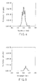
FIG. 4 is a diagram showing a measurement result of the semiconductor device (light emitting diode) according to the present embodiment. Specifically, the figure shows the measurement result by micro photoluminescence (PL). As shown inFIG. 4 , a green light emitting spectrum with a very strong light emitting intensity, whose center wavelength is 495 nm, is obtained. -
FIG. 5 is a diagram showing a measurement result of a semiconductor device (light emitting diode) according to a first comparative example of the present embodiment. In the first comparative example, the In composition of the quantum well layer is as high as 0.35 for making the barrier layer of InGaN and for elongating the light emitting wavelength. The light emitting intensity is more largely lowered in the comparative example than in the present embodiment. In the comparative example, it is assumed that since the In composition of the quantum well layer is high for achieving an elongated wavelength, the light emitting efficiency is largely lowered from the aforementioned reasons. -
FIG. 6 is a diagram showing a measurement result of a semiconductor device (light emitting diode) according to a second comparative example of the present embodiment. In the second comparative example, the barrier layer and the quantum well layer are stacked without providing the intermediate layer. The light emitting intensity is more largely lowered in the comparative example than in the present embodiment. In the comparative example, it is assumed that since the barrier layer and the quantum well layer are directly stacked without the intermediate layer, the light emitting efficiency is largely lowered from the aforementioned reasons. - Generally, the Al composition of the barrier layer is preferably in the range of 0.2 to 0.4 and the In composition of the barrier layer is preferably in the range of 0.01 to 0.05. The thickness of the barrier layer is preferably in the range of 4 to 20 nm. Further, the intermediate layer preferably has an In composition equal to or higher than that of the barrier layer. Particularly, the In composition of the intermediate layer is preferably in the range of 0.01 to 0.05 similarly as the In composition of the barrier layer. In this manner, the drastic lattice mismatch can be restricted, thereby effectively restricting the occurrence of phase separation or defect. The In composition of the quantum well layer is preferably in the range of 0.1 to 0.3. This is because when the In composition of the quantum well layer is set to be higher than 0.3, an influence of the piezoelectric field is noticeable and the light emitting efficiency can be largely lowered. It is preferable to set the In composition of the quantum well layer at 0.3 or less and to adjust the Al composition of the barrier layer for controlling the light emitting wavelength. Furthermore, the thickness of the intermediate layer is preferably in the range of 0.5 to 1.5 nm.
- Next, a second embodiment according to the present invention will be described. A basic structure thereof is similar as in the first embodiment, and the description of the concerns described in the first embodiment will be omitted.
-
FIG. 7 is a cross sectional view schematically showing a structure of the semiconductor device (light emitting diode) according to the present embodiment. - A sapphire substrate is employed for the
substrate 10, and the upper surface (device forming surface) of thesapphire substrate 10 is the (0001) surface of sapphire crystal, that is, the C surface. An n-typeGaN contact layer 21, an n-typeGaN guide layer 22, thelight emitting layer 30 having a multi quantum well structure, a p-type AlGaNoverflow preventing layer 41, a p-type GaN layer 42 and a p-typeGaN contact layer 43 are stacked on the upper surface (C surface) of thesapphire substrate 10. Further, an n-side electrode 50 made of Ti/Pt/Au is formed on the exposed surface of the n-typeGaN contact layer 21. Furthermore, a p-side electrode 60 made of Ni/Au is formed on the surface of the p-typeGaN contact layer 43. The structure of thelight emitting layer 30 is similar to the structure explained in the first embodiment. - The overflow preventing layer is effective in the high power light emitting diode having the current density of, for example, about 100 A/cm2 or more. As the overflow preventing layer, a layer having the composition of p-InuAlvGa1-u-vN (0=<u<1, 0<v<1) can be used in addition to the above example. In this case, it is preferable that the overflow preventing layer has the Al composition higher than that of the barrier layer.
- Also in the present embodiment, since the structure of the
light emitting layer 30 is similar as the structure explained in the first embodiment, similar effects as those explained in the first embodiment can be obtained. - In the following, a method for manufacturing the semiconductor device (light emitting diode) according to the present embodiment will be described.
- Each layer of the present semiconductor device is formed by the metal organic chemical vapor deposition (MOCVD) method. The materials therefor may employ trimethyl gallium (TMG), trimethyl aluminum (TMA), trimethyl indium (TMI) and bis (cyclopentadienyl) magnesium) (Cp2Mg). The gas material may employ ammonia (NH3) and silane (SiH4). The carrier gas may employ hydrogen and nitrogen.
- At first, the sapphire substrate processed by organic cleaning and acid cleansing is introduced into a reaction chamber of the MOCVD apparatus and is put on a susceptor to be heated by high frequency.
- Subsequently, the sapphire substrate is raised in its temperature to 1100°C for 12 minutes under a nitrogen/hydrogen atmosphere at a normal pressure. In the temperature rising process, gas phase etching is performed on the substrate surface to remove a native oxide film on the substrate surface.
- Next, nitrogen/hydrogen is employed as a carrier gas to supply ammonia at a flow rate of 6 L/minute, TMG at a flow rate of 50 cc/minute and SiH4 at a flow rate of 10 cc/minute, for 60 minutes, thereby forming the n-type
GaN contact layer 21. Subsequently, the temperature is lowered to 1060°C and SiH4 is lowered in its flow rate to 3 cc/minute, thereby forming the n-typeGaN guide layer 22 for about 3 minutes. - Next, the supply of TMG and SiH4 is stopped to lower the substrate temperature to 800°C. The carrier gas is switched to only nitrogen, and ammonia and TMG are supplied at a flow rate of 12 L/minute and at a flow rate of 3 cc/minute, respectively. After TMI and SiH4 are supplied therein at a flow rate of 5 cc/minute and at a flow rate of 1 cc/minute, respectively, for two minutes, TMA is further added at a flow rate of 16 cc/minute and supplied for 12 minutes. Thereafter, the supply of TMA is stopped and the growth is performed for two minutes with TMG and SiH4 being supplied. Thereafter, the amount of supply of TMI is increased to 80 cc/minute and the growth is performed for 40 seconds. A series of processings is repeated five times, and TMG and TMI are finally supplied at a flow rate of 3 cc/minute and at a flow rate of 5 cc/minute, respectively, for about 14 minutes, thereby forming the
light emitting layer 30 having a multi quantum well structure. The processing may not be repeated five times in the same structure. The flow rate of TMG, TMA or TMI may be varied, and the Al composition and In composition may be inclined in thebarrier layer 31 and theintermediate layer 32. The cycle of the multi quantum well structure is not limited to 5. It can be selected in the range of 2 to 10. - Next, the supply of TMG and TMI is stopped to raise the temperature to 1030°C with nitrogen and ammonia being supplied. The flow rate of ammonia is switched to 4 L/minute under the nitrogen/hydrogen atmosphere while the temperature is being held at 1030°C. TMG, TMA and Cp2Mg are supplied therein at a flow rate of 25 cc/minute, a flow rate of about 30 cc/minute and a flow rate of 6 cc/minute, respectively, for one minute to form the p-type AlGaN
overflow preventing layer 41. The Al composition of p-type AlGaN is 0.2 or more. It is preferable that the Al composition of p-type AlGaN is higher than the Al composition of theInAlGaN barrier layer 31. This prevents the overflow of electron, and it is preferable for the semiconductor device which is used at high current density. - Then, the supply of only TMA is stopped from the above state to switch the flow rate of Cp2Mg to 8 cc/minute for supply for about 6 minutes, thereby forming the p-
type GaN layer 42. - Then, Cp2Mg is supplied at a flow rate of 50 cc/minute for about three minutes from the above state, thereby forming the p-type
GaN contact layer 43. Subsequently, the supply of organic metal material is stopped and only the carrier gas is continuously supplied so that the substrate temperature naturally decreases. The supply of ammonia stops when the substrate temperature reaches 500°C. - Next, part of the multilayered structure obtained in the above manner is removed by dry etching until it reaches the n-type
GaN contact layer 21, and the n-side electrode 50 made of Ti/Pt/Au is formed on the exposedcontact layer 21. Further, the p-side electrode 60 made of Ni/Au is formed on the p-typeGaN contact layer 43. - Then, when the I-V characteristic is measured on the semiconductor device (light emitting diode) having the structure obtained in the above manner, an excellent characteristic can be obtained. The operating voltage of the light emitting diode is 3.5 to 4 V at 20 mA and the light output is 10 mW. A peak with wavelength center of 500 nm is obtained from the wavelength measurement.
- The sapphire substrate was employed as the substrate in the first and second embodiments described above, but a GaN substrate, SiC substrate, ZnO substrate or the like may be employed. Further, the device forming surface is not limited to the C surface and each layer may be formed on a nonpolar surface. It is possible to apply a structure in which an electrode is provided on the backside of the wafer. Furthermore, it is possible to obtain a blue light emitting diode with high light emitting efficiency, in addition to a green light emitting diode with high light emitting efficiency.
Claims (7)
- A semiconductor device characterized by comprising:an underlying layer; anda light emitting layer which is formed on the underlying layer and in which a barrier layer made of InAlGaN and a quantum well layer made of InGaN are alternately stacked.
- The semiconductor device according to claim 1, characterized in that the barrier layer has an In composition lower than that of the quantum well layer.
- The semiconductor device according to claim 2, characterized by further comprising an intermediate layer provided between the barrier layer and the quantum well layer adjacent to each other, made of InGaN and having an In composition lower than that of the quantum well layer.
- The semiconductor device according to claim 3, characterized by further comprising an overflow preventing layer formed on the light emitting layer and having an Al composition higher than that of the barrier layer.
- The semiconductor device according to claim 3, characterized by further comprising a p-InuAlvGa1-u-vN (0=<u<1, 0<v<1) layer formed on the light emitting layer.
- The semiconductor device according to claim 2, characterized in that the underlying layer is made of GaN.
- The semiconductor device according to claim 6, characterized in that the underlying layer is substantially formed on (0001) surface of a substrate.
Applications Claiming Priority (2)
| Application Number | Priority Date | Filing Date | Title |
|---|---|---|---|
| JP2008221471 | 2008-08-29 | ||
| PCT/JP2009/065195 WO2010024436A1 (en) | 2008-08-29 | 2009-08-31 | Semiconductor device |
Publications (2)
| Publication Number | Publication Date |
|---|---|
| EP2325899A1 true EP2325899A1 (en) | 2011-05-25 |
| EP2325899A4 EP2325899A4 (en) | 2015-04-29 |
Family
ID=41721595
Family Applications (1)
| Application Number | Title | Priority Date | Filing Date |
|---|---|---|---|
| EP09810080.3A Withdrawn EP2325899A4 (en) | 2008-08-29 | 2009-08-31 | SEMICONDUCTOR DEVICE |
Country Status (6)
| Country | Link |
|---|---|
| US (1) | US20100187497A1 (en) |
| EP (1) | EP2325899A4 (en) |
| JP (2) | JP2010080955A (en) |
| KR (1) | KR20110034689A (en) |
| CN (1) | CN102138227A (en) |
| WO (1) | WO2010024436A1 (en) |
Families Citing this family (27)
| Publication number | Priority date | Publication date | Assignee | Title |
|---|---|---|---|---|
| JP4881491B2 (en) | 2009-09-01 | 2012-02-22 | 株式会社東芝 | Semiconductor light emitting device |
| JP4940317B2 (en) * | 2010-02-25 | 2012-05-30 | 株式会社東芝 | Semiconductor light emitting device and manufacturing method thereof |
| JP5325171B2 (en) * | 2010-07-08 | 2013-10-23 | 株式会社東芝 | Semiconductor light emitting device |
| US9142413B2 (en) * | 2010-11-08 | 2015-09-22 | Georgia Tech Research Corporation | Methods for growing a non-phase separated group-III nitride semiconductor alloy |
| US20130082274A1 (en) * | 2011-09-29 | 2013-04-04 | Bridgelux, Inc. | Light emitting devices having dislocation density maintaining buffer layers |
| KR101262726B1 (en) * | 2011-12-30 | 2013-05-09 | 일진엘이디(주) | Nitride based light emitting device with p-type nitride layer |
| EP2820678B1 (en) * | 2012-02-28 | 2019-05-08 | Lumileds Holding B.V. | Integration of gallium nitride leds with aluminum gallium nitride/gallium nitride devices on silicon substrates for ac leds |
| CN105051918A (en) * | 2013-03-15 | 2015-11-11 | 索泰克公司 | Semiconductor structures having active regions comprising ingan, methods of forming such semiconductor structures, and light emitting devices formed from such semiconductor structures |
| US9343626B2 (en) | 2013-03-15 | 2016-05-17 | Soitec | Semiconductor structures having active regions comprising InGaN, methods of forming such semiconductor structures, and light emitting devices formed from such semiconductor structures |
| FR3003397B1 (en) * | 2013-03-15 | 2016-07-22 | Soitec Silicon On Insulator | Semiconductor structures with active regions including INGAN |
| TWI593135B (en) | 2013-03-15 | 2017-07-21 | 索泰克公司 | Semiconductor structure having an active region containing indium gallium nitride, a method of forming such a semiconductor structure, and a light-emitting element formed using the semiconductor structure |
| JP5606595B2 (en) * | 2013-06-28 | 2014-10-15 | 株式会社東芝 | Manufacturing method of semiconductor light emitting device |
| FR3012676A1 (en) | 2013-10-25 | 2015-05-01 | Commissariat Energie Atomique | QUANTUM WELL ELECTROLUMINESCENT DIODE SEPARATED BY BARRIER LAYERS OF INGAN HAVING VARIABLE INDIUM COMPOSITIONS |
| JP6281469B2 (en) * | 2014-11-03 | 2018-02-21 | 豊田合成株式会社 | Method for manufacturing light emitting device |
| US9985168B1 (en) | 2014-11-18 | 2018-05-29 | Cree, Inc. | Group III nitride based LED structures including multiple quantum wells with barrier-well unit interface layers |
| CN107207960B (en) * | 2015-02-02 | 2021-05-25 | 斯坦雷电气株式会社 | Manufacturing method of quantum dots and quantum dots |
| JP6764231B2 (en) * | 2015-02-06 | 2020-09-30 | スタンレー電気株式会社 | Manufacturing method of semiconductor nanoparticles and semiconductor nanoparticles |
| JP6764230B2 (en) * | 2015-02-06 | 2020-09-30 | スタンレー電気株式会社 | Manufacturing method of semiconductor nanoparticles |
| JP6128138B2 (en) * | 2015-02-10 | 2017-05-17 | ウシオ電機株式会社 | Semiconductor light emitting device |
| DE102016116425B4 (en) | 2016-09-02 | 2026-04-23 | OSRAM Opto Semiconductors Gesellschaft mit beschränkter Haftung | Optoelectronic component |
| US11393948B2 (en) | 2018-08-31 | 2022-07-19 | Creeled, Inc. | Group III nitride LED structures with improved electrical performance |
| JP6891865B2 (en) | 2018-10-25 | 2021-06-18 | 日亜化学工業株式会社 | Light emitting element |
| US11923398B2 (en) | 2019-12-23 | 2024-03-05 | Lumileds Llc | III-nitride multi-wavelength LED arrays |
| US11404473B2 (en) | 2019-12-23 | 2022-08-02 | Lumileds Llc | III-nitride multi-wavelength LED arrays |
| KR20220162167A (en) | 2020-05-04 | 2022-12-07 | 구글 엘엘씨 | Light emitting diode including an aluminum-containing layer therein and method related thereto |
| US11631786B2 (en) * | 2020-11-12 | 2023-04-18 | Lumileds Llc | III-nitride multi-wavelength LED arrays with etch stop layer |
| CN115458649B (en) * | 2022-10-21 | 2025-05-02 | 江西兆驰半导体有限公司 | Light-emitting diode epitaxial wafer and preparation method thereof, and light-emitting diode |
Family Cites Families (19)
| Publication number | Priority date | Publication date | Assignee | Title |
|---|---|---|---|---|
| US5684309A (en) * | 1996-07-11 | 1997-11-04 | North Carolina State University | Stacked quantum well aluminum indium gallium nitride light emitting diodes |
| JPH1065271A (en) * | 1996-08-13 | 1998-03-06 | Toshiba Corp | Gallium nitride based semiconductor light emitting device |
| JP3304782B2 (en) * | 1996-09-08 | 2002-07-22 | 豊田合成株式会社 | Semiconductor light emitting device |
| JPH10270756A (en) * | 1997-03-27 | 1998-10-09 | Sanyo Electric Co Ltd | Gallium nitride compound semiconductor device |
| JP3519990B2 (en) * | 1998-12-09 | 2004-04-19 | 三洋電機株式会社 | Light emitting device and manufacturing method thereof |
| JP4032636B2 (en) * | 1999-12-13 | 2008-01-16 | 日亜化学工業株式会社 | Light emitting element |
| JP4724901B2 (en) | 2000-07-21 | 2011-07-13 | パナソニック株式会社 | Manufacturing method of nitride semiconductor |
| EP1385241B1 (en) * | 2001-03-28 | 2008-12-31 | Nichia Corporation | Nitride semiconductor element |
| JP4161603B2 (en) * | 2001-03-28 | 2008-10-08 | 日亜化学工業株式会社 | Nitride semiconductor device |
| CN100521260C (en) * | 2002-07-16 | 2009-07-29 | 氮化物半导体株式会社 | Gallium nitride-based compound semiconductor device |
| JP2004200347A (en) * | 2002-12-18 | 2004-07-15 | Sumitomo Electric Ind Ltd | Light emitting diode with high heat dissipation performance |
| US20040161006A1 (en) * | 2003-02-18 | 2004-08-19 | Ying-Lan Chang | Method and apparatus for improving wavelength stability for InGaAsN devices |
| JP4412918B2 (en) * | 2003-05-28 | 2010-02-10 | シャープ株式会社 | Nitride semiconductor light emitting device and manufacturing method thereof |
| JP2004015072A (en) * | 2003-09-26 | 2004-01-15 | Nichia Chem Ind Ltd | Nitride semiconductor light emitting device |
| JP4389723B2 (en) * | 2004-02-17 | 2009-12-24 | 住友電気工業株式会社 | Method for forming a semiconductor device |
| CN100349306C (en) * | 2004-08-27 | 2007-11-14 | 中国科学院半导体研究所 | Blue light and yellow light quantum sink heap structure white light emitting diode and producing method |
| JP2007088270A (en) * | 2005-09-22 | 2007-04-05 | Matsushita Electric Works Ltd | Semiconductor light emitting element, lighting device using the same and manufacturing method of semiconductor light emitting element |
| JP2007214221A (en) * | 2006-02-08 | 2007-08-23 | Sharp Corp | Nitride semiconductor laser device |
| KR100753518B1 (en) * | 2006-05-23 | 2007-08-31 | 엘지전자 주식회사 | Nitride-based light emitting device |
-
2009
- 2009-08-31 WO PCT/JP2009/065195 patent/WO2010024436A1/en not_active Ceased
- 2009-08-31 KR KR1020117004435A patent/KR20110034689A/en not_active Ceased
- 2009-08-31 JP JP2009201071A patent/JP2010080955A/en active Pending
- 2009-08-31 EP EP09810080.3A patent/EP2325899A4/en not_active Withdrawn
- 2009-08-31 CN CN2009801334030A patent/CN102138227A/en active Pending
-
2010
- 2010-03-03 US US12/716,668 patent/US20100187497A1/en not_active Abandoned
-
2011
- 2011-09-26 JP JP2011209882A patent/JP5634368B2/en active Active
Also Published As
| Publication number | Publication date |
|---|---|
| WO2010024436A1 (en) | 2010-03-04 |
| KR20110034689A (en) | 2011-04-05 |
| JP5634368B2 (en) | 2014-12-03 |
| JP2011258994A (en) | 2011-12-22 |
| US20100187497A1 (en) | 2010-07-29 |
| EP2325899A4 (en) | 2015-04-29 |
| JP2010080955A (en) | 2010-04-08 |
| CN102138227A (en) | 2011-07-27 |
Similar Documents
| Publication | Publication Date | Title |
|---|---|---|
| US20100187497A1 (en) | Semiconductor device | |
| US8513694B2 (en) | Nitride semiconductor device and manufacturing method of the device | |
| CN115995514B (en) | A quantum well LED with AlGaN/InGaN superlattice barrier layer and its preparation method | |
| EP2518783B1 (en) | Nitride semiconductor light-emitting element and method for manufacturing same | |
| CN101188264B (en) | Nitride semiconductor light emitting device | |
| US20030211645A1 (en) | Gallium nitride-based semiconductor light emitting device and method | |
| US9755107B2 (en) | Group III nitride semiconductor light-emitting device | |
| US8716048B2 (en) | Light emitting device and method for manufacturing the same | |
| TW201011952A (en) | Group iii nitride based semiconductor light emitting element and epitaxial wafer | |
| JP2014518448A (en) | Low droop light emitting diode structure on gallium nitride semipolar substrate | |
| US20120138891A1 (en) | METHOD FOR REDUCTION OF EFFICIENCY DROOP USING AN (Al,In,Ga)N/Al(x)In(1-x)N SUPERLATTICE ELECTRON BLOCKING LAYER IN NITRIDE BASED LIGHT EMITTING DIODES | |
| EP2270879A1 (en) | Nitride semiconductor light emitting element | |
| CN103730557A (en) | Light-emitting diode with novel P-type electron barrier layer structure and growth method | |
| WO2017202328A1 (en) | Gallium nitride-based light emitting diode and preparation method therefor | |
| WO2015146069A1 (en) | Light emitting diode element | |
| CN108447952A (en) | A light-emitting diode epitaxial wafer and its preparation method | |
| US20120126283A1 (en) | High power, high efficiency and low efficiency droop iii-nitride light-emitting diodes on semipolar substrates | |
| EP2290708B1 (en) | Light-emitting element and a production method therefor | |
| US9818907B2 (en) | LED element | |
| CN118738241B (en) | Light emitting diode epitaxial wafer and preparation method thereof, LED | |
| Zakheim et al. | Blue LEDs–way to overcome efficiency droop | |
| CN104112799A (en) | Lattice-matched LED epitaxial structure and preparation method thereof | |
| WO2012058426A1 (en) | Light emitting diode for droop improvement | |
| KR20230015734A (en) | Light emitting device and method for manufacturing the same | |
| CN119230672B (en) | LED epitaxial wafer, preparation method thereof and LED |
Legal Events
| Date | Code | Title | Description |
|---|---|---|---|
| PUAI | Public reference made under article 153(3) epc to a published international application that has entered the european phase |
Free format text: ORIGINAL CODE: 0009012 |
|
| 17P | Request for examination filed |
Effective date: 20110223 |
|
| AK | Designated contracting states |
Kind code of ref document: A1 Designated state(s): AT BE BG CH CY CZ DE DK EE ES FI FR GB GR HR HU IE IS IT LI LT LU LV MC MK MT NL NO PL PT RO SE SI SK SM TR |
|
| AX | Request for extension of the european patent |
Extension state: AL BA RS |
|
| DAX | Request for extension of the european patent (deleted) | ||
| RA4 | Supplementary search report drawn up and despatched (corrected) |
Effective date: 20150327 |
|
| RIC1 | Information provided on ipc code assigned before grant |
Ipc: H01L 33/06 20100101AFI20150323BHEP Ipc: H01L 33/32 20100101ALI20150323BHEP |
|
| STAA | Information on the status of an ep patent application or granted ep patent |
Free format text: STATUS: THE APPLICATION HAS BEEN WITHDRAWN |
|
| 18W | Application withdrawn |
Effective date: 20150601 |