JP4724901B2 - Manufacturing method of nitride semiconductor - Google Patents
Manufacturing method of nitride semiconductor Download PDFInfo
- Publication number
- JP4724901B2 JP4724901B2 JP2000220454A JP2000220454A JP4724901B2 JP 4724901 B2 JP4724901 B2 JP 4724901B2 JP 2000220454 A JP2000220454 A JP 2000220454A JP 2000220454 A JP2000220454 A JP 2000220454A JP 4724901 B2 JP4724901 B2 JP 4724901B2
- Authority
- JP
- Japan
- Prior art keywords
- barrier layer
- layer
- nitride semiconductor
- substrate
- growth
- Prior art date
- Legal status (The legal status is an assumption and is not a legal conclusion. Google has not performed a legal analysis and makes no representation as to the accuracy of the status listed.)
- Expired - Fee Related
Links
Images


Landscapes
- Chemical Vapour Deposition (AREA)
- Semiconductor Lasers (AREA)
- Led Devices (AREA)
Description
【0001】
【発明の属する技術分野】
本発明は発光ダイオードや半導体レーザダイオード等の光デバイスに利用される窒化物半導体の製造方法に関する。
【0002】
【従来の技術】
III族元素としてAl、Ga、In等を含み、5族元素としてN等を含むAlGaInNで表される窒化物半導体は、可視光の発光デバイスや高温動作電子デバイス用の半導体材料として多用されるようになっており、青色や緑色の発光ダイオードや、青紫色のレーザダイオードの分野で実用化が進んでいる。
【0003】
この窒化物半導体を用いた発光素子の製造においては、有機金属気相成長(MOCVD)法によって窒化物半導体薄膜結晶を成長させるのが近来では主流である。この方法は、サファイアやSiC、GaN等からなる基板を設置した反応管内にIII族元素の原料ガスとして有機金属化合物ガス(トリメチルガリウム(以下、「TMG」と略称する。)、トリメチルアルミニウム(以下、「TMA」と略称する。)、トリメチルインジウム(以下、「TMI」と略称する。)等)と、V族元素の原料ガスとしてアンモニアやヒドラジン等を供給し、基板温度をおよそ700℃〜1100℃の高温で保持して、基板上にn型層と発光層とp型層とを成長させてこれらを積層形成するというものである。n型層の成長時にはn型不純物原料ガスとしてモノシラン(SiH4)やゲルマン(GeH4)等を、p型層の成長時にはp型不純物原料ガスとしてシクロペンタジエニルマグネシウム(Cp2Mg)やジメチル亜鉛(Zn(CH3)2)等をIII族元素の原料ガスと同時に流しながら成長させる。
【0004】
そして、この成長形成の後、n型層の表面およびp型層の表面のそれぞれにn側電極およびp側電極を形成し、チップ状に分離することによって、発光素子を得ることができる。
【0005】
発光層は、所望の発光波長となるようにInの組成を調整したInGaNを用い、これを発光層よりバンドギャップエネルギーの大きいクラッド層で挟み込んだダブルヘテロ構造や、更に発光層を量子サイズ効果が生じるような薄い層で形成した量子井戸構造が一般的に用いられているが、最近では、発光効率の高い量子井戸構造の方が主流となっている。
【0006】
この量子井戸構造は井戸層と呼ばれるバンドギャップエネルギーの小さい層を井戸層よりもバンドギャップエネルギーの大きい層で挟み込むことによって形成される。
【0007】
また、井戸層が一つである単一量子井戸よりも発光効率の高い多重量子井戸(MQW)は、InxGa1-xN(0<x<1)からなる井戸層と、InyAlzGa1-y-zN(0≦y<1、0≦z<1、0≦y+z<1、x>y)からなる障壁層を交互に積層することによって形成され、従来のMQWの作製方法としては以下の3通りに大別される。
【0008】
第一の従来の技術は、特開平10−12922号公報に開示されている。これは、AlGaNからなる障壁層とInGaNからなる井戸層を交互に積層したMQWからなる窒化物半導体発光素子であり、MOCVD装置を用いて、サファイア基板上にAlNからなるバッファ層、Siをド−プしたGaN層を順次に積層した後、MQWからなる発光層を積層し、その上にMgをドープしたクラッド層及びコンタクト層を順次に積層したものである。
【0009】
この発光素子におけるMQWの成長方法については、まず基板温度を1100℃に保持し、N2又はH2、アンモニア、TMG、TMAを導入してAl0.05Ga0.95Nからなる厚さ50Åの障壁層を形成し、続いて基板温度を800℃に下げて保持し、N2又はH2、アンモニア、TMG、TMIを供給し、シリコンと亜鉛がド−プされたIn0.20Ga0.80Nからなる厚さ50Åの井戸層を形成する。そして、前記障壁層と前記井戸層を交互に成長し、全体の厚さが0.055μmのMQWからなる発光層を形成する。この時、障壁層は井戸層の成長速度と同じにしている。
【0010】
この構造では、発光層に井戸層と障壁層との歪超格子からなるMQWを用いているため、転位の少ない良質な結晶を得ることができ、窒化物半導体発光素子の発光効率が向上することが示されている。
【0011】
第二の従来の技術は、特開平10−135514号公報に開示されている。これは、前記発光素子のMQWの成長方法において、基板温度を900℃に保持し、N2、TMG、アンモニアを導入して厚さ3.5nmのGaNからなる障壁層を形成する。次に、基板温度を750℃に保持しN2、TMG、アンモニアの他に、TMIを導入して厚さ3.5nmのIn0.16Ga0.84Nからなる井戸層を形成する。そして、前記障壁層と前記井戸層を交互に成長し、5層の障壁層と井戸層を形成する。さらに、基板温度を900℃に保持し、14nmのGaNからなる最上の障壁層を5段目の量子井戸層上に形成する。この時、障壁層は井戸層の成長速度と同じにしている。
【0012】
この構造では、Siド−プのGaN層およびMgド−プのクラッド層に接する側の層を障壁層とし、かつ各障壁層の厚みを均一にすることによって、発光する光の波長シフトが防止できることが示されている。
第三の従来の技術は、特開平11−224972号公報に開示されている。これは、前記発光素子のMQWの成長方法において、基板温度を750℃に保持して、In0.2Ga0.8Nからなる井戸層を25Åの膜厚で形成する。次に、TMIのモル比を変化させるのみで同じ基板温度で、In0.01Ga0.95Nからなる障壁層を50Åの膜厚で形成する。この操作を13回繰り返し、最後に井戸層を形成し、総膜厚が0.1μmの多重量子井戸構造からなる活性層を形成する。この時、障壁層は井戸層の成長速度と同じにしている。
【0013】
この例では、障壁層を井戸層よりもバンドギャップの大きいInGaNとして形成したものであり、井戸層の上にInGaNからなる障壁層を形成した場合、InGaNからなる障壁層はGaNやAlGaN結晶に比較して結晶が柔らかいため、MQWよりも上のクラッド層にクラックが発生し難くなり、前記クラッド層を厚くできるため、特に窒化物半導体からなる半導体レ−ザの高品質化に有効であることが示されている。
【0014】
また、障壁層もInGaNの場合、井戸層と障壁層が同じ温度で成長できるため、先に形成した井戸層の分解が抑制されるので、結晶性のよいMQWを形成できるし、井戸層と障壁層を連続して成長できるので、MQWの成長時間も短縮できることが示されている。
【0015】
【発明が解決しようとする課題】
しかしながら、前述のようなMQWの形成方法においては以下のような問題点がある。
【0016】
まず、第一の従来の技術においては、InGaNからなる井戸層を成長後、AlGaNからなる障壁層を成長させる基板温度(1100℃)まで昇温する過程において、井戸層が分解してしまうため、結晶性のすぐれた井戸層を成長させることは困難である。
【0017】
次に、第二の従来の技術においても、InGaNからなる井戸層を成長後、GaNからなる障壁層を成長させる基板温度(900℃)まで昇温する過程において、少なくとも井戸層の分解が発生するため、結晶性のすぐれた井戸層を成長させることは困難である。
【0018】
一方、第三の従来の技術においては、井戸層と障壁層を成長させる基板温度が同じであるため、井戸層の分解は少ない。しかしながら、MQWにおいて、障壁層が十分機能するためには、障壁層は井戸層に比較して十分低いIn組成にする必要がある。この例では、障壁層のIn組成は0.01であり、このような低いIn組成を制御することは困難である。
【0019】
また、前記障壁層のInGaNは、実質的にはGaNに近い結晶である。これより、GaNに近い結晶である障壁層を井戸層と同じ基板温度(750℃)で成長させることになるため、障壁層の結晶性は従来の技術1の1100℃付近で成長した場合に比較して悪くなる。
【0020】
このように、従来のMQWの製造方法では、障壁層の結晶性向上のために、障壁層を成長させる基板温度を井戸層を成長させる基板温度よりも上げると井戸層が劣化し、障壁層と井戸層を同じ基板温度で成長させると、障壁層の結晶性が不十分となり、MQWの品質が低下するという問題があった。
【0021】
また、高品質なMQWを作製するためには、障壁層は井戸層に比較して厚く形成する必要がある。前記3つの従来の技術に共通するように、障壁層と井戸層を同じ成長速度で成長させる方法では、障壁層を厚くした場合やMQWの周期数を増やした場合に成長時間が長くなり、MQWの製造コストが高くなる上、MQWの結晶性が低下するという問題があった。
【0022】
本発明において解決すべき課題は、井戸層の劣化を抑制し、かつ障壁層の結晶性を向上させることで、発光効率の向上したMQWの製造方法を提供することと、MQWの形成時間の短縮化により製造コストを低減した窒化物半導体からなる発光素子の製造方法を提供することである。
【0023】
【課題を解決するための手段】
本発明者らは、MQWの製造方法(特に、基板温度、成長速度、雰囲気の水素濃度及びV/III比)について鋭意検討を行った。その結果、井戸層の成長に適した基板温度で井戸総を成長した後に、基板を昇温しながら障壁層の一部(以下、「障壁層A」と略称する。)を成長し、さらに昇温後に略一定の基板温度で障壁層の一部(以下、「障壁層B」と略称する。)を成長した後、基板温度を井戸層を成長させる温度まで降温し、井戸層を成長させるといった工程を繰り返すことにより、結晶性に優れ、発光効率の高いMQW発光層を形成できることを見出した。
【0024】
次に、障壁層Bを成長させる際に、雰囲気の水素濃度を障壁層Aを成長させる場合よりも高くすることや、V/III比を障壁層Aを成長させる場合よりにすることによって、障壁層Bの結晶性を改善できることを見出した。
【0025】
また、障壁層Bを成長させる際に、井戸層および障壁層Aよりも速い成長速度で成長させることや、障壁層Bを成長した後、井戸層を成長させる基板温度まで降温する際にも、少なくとも障壁層の一部を成長させる工程を加えることによって、障壁層が厚い場合や、MQWの周期数が多い場合でも、MQWの形成時間がさらに短縮できることを見出した。
【0026】
このような構成によれば、MQWの形成時において、井戸層の分解を抑制できると同時に、障壁層の結晶性を向上させることができ、発光効率の高いMQW発光層を作製することが可能となる。また、MQW発光層の形成時間を短縮化することができるため、窒化物半導体からなる発光素子の製造コストを低減することが可能となる。
【0027】
【発明の実施の形態】
本願第1の発明は、基板の上に、窒化物半導体からなる井戸層と、前記井戸層よりもバンドギャップエネルギーが大きい窒化物半導体からなる障壁層と、を交互に積層した多重量子井戸構造を有する窒化物半導体を製造する方法であって、第1の基板温度で前記井戸層を成長させる第1の工程と、前記第1の基板温度から前記第1の基板温度より高い第2の基板温度に向かって昇温しながら前記障壁層を成長させる第2の工程と、前記第2の基板温度から前記第1の基板温度に降温する第3の工程と、を順に繰り返すことによって多重量子井戸を形成することを特徴とする窒化物半導体の製造方法である。
【0028】
この方法は、井戸層の成長直後より、昇温しながら障壁層を成長させるので、昇温時におけるInGaNからなる井戸層の分解が抑制できると同時に、障壁層の結晶性を高めることができるという作用を有する。
【0029】
本願第2の発明は、前記第2の工程により前記障壁層を成長させた後、前記第3の工程の前に、前記第2の基板温度を略一定に保った基板温度で更に前記障壁層を成長させる第4の工程を設けることを特徴とする窒化物半導体の製造方法であり、井戸層を成長させる基板温度より高い基板温度で保持した状態において、障壁層の一部を成長させるので、障壁層の結晶性をさらに高めることができるという作用を有する。
【0030】
本願第3の発明は、前記第4の工程における前記障壁層の成長の少なくとも一部における成長速度が、前記第2の工程における前記障壁層の成長速度より大きいことを特徴とする窒化物半導体の製造方法であり、井戸層よりも相対的に厚い障壁層や周期数の多いMQWを短時間で成長でき、ト−タルのMQWの成長時間を短縮できるため、MQWからなる窒化物半導体の製造コストを低減できるという作用を有する。
【0031】
本願第4の発明は、前記第4の工程における前記障壁層の成長時の少なくとも一部における雰囲気中の水素濃度が、前記第2の工程における前記障壁層の成長時の雰囲気中の水素濃度より大きいことを特徴とする窒化物半導体の製造方法であり、前記第4の工程で水素濃度を高めることにより、基板表面での原子のマイグレ−ションが促進され、障壁層の結晶性をさらに高めることができるという作用を有する。
【0032】
本願第5の発明は、前記第4の工程における前記障壁層の成長時の少なくとも一部におけるIII族原料供給量に対するV族原料供給量の比(以下V/III比と呼ぶ)が、前記第2の工程における前記障壁層の成長時のV/III比より小さいことを特徴とする窒化物半導体の製造方法であり、障壁層Bを成長させる際に、障壁層Bの結晶性を悪化させずにアンモニアの供給量を大幅に低減でき、MQWからなる窒化物半導体の製造コストを低減できるという作用を有する。
【0033】
本願第6の発明は、前記井戸層がInxGa1-xN(但し、0<x<1)であり、前記障壁層がInyAlzGa1-y-zN(但し、0≦y<1、0≦z<1、0≦y+z<1、x>y)であることを特徴とする窒化物半導体の製造方法であり、井戸層及び障壁層を構成する窒化物半導体材料を上記の材料に限定することで、MQWを高品質化することができ、光学的特性のすぐれたMQWからなる窒化物半導体を作製できるという作用を有する。
【0034】
本願第7の発明は、前記障壁層がGaNであることを特徴とする窒化物半導体の製造方法であり、障壁層の結晶性をさらに高めることができ、光学特性のすぐれたMQWからなる窒化物半導体を作製できるという作用を有する。
【0035】
本願第8の発明は、前記第1の基板温度が500℃〜900℃であり、前記第2の基板温度が800℃〜1200℃であることを特徴とする窒化物半導体の製造方法であり、前記第1の基板温度および前記第2の基板温度を上記の範囲に限定することにより、結晶性のすぐれた井戸層及び障壁層を作製できるという作用を有する。
【0036】
本願第9の発明は、前記障壁層の成長開始時のGa原料供給量が、前記井戸層の成長時のGa原料供給量より少ないことを特徴とする窒化物半導体の製造方法であり、井戸層の劣化が抑制できると同時に、障壁層の結晶性を高めることができるという作用を有する。
【0037】
本願第10の発明は、前記第3の工程の少なくとも一部において、前記障壁層を成長させることを特徴とする窒化物半導体の製造方法であり、降温時にも障壁層の一部を成長させることにより、特に障壁層を厚くする場合やMQWの周期数を多くする場合でもMQWの形成時間を短縮化することができ、MQWからなる窒化物半導体の製造コストを低減することできるという作用を有する。
【0038】
本願第11の発明は、前記基板がサファイアまたはSiCを含み、前記第1の基板温度より低温の基板温度で前記基板の上に窒化物半導体を含むバッファ層を形成し、前記バッファ層の上に窒化物半導体を含む下地層を形成し、前記下地層の上に前記多重量子井戸を形成することを特徴とする窒化物半導体の製造方法であり、高い結晶性をもつ下地層を作製でき、その上に成長させるMQWを高品質化できるため、MQWからなる発光層をもつ窒化物半導体発光素子の発光効率を高めることができるという作用を有する。
【0039】
本願第12の発明は、前記基板が窒化物半導体を含み、前記基板の上に窒化物半導体を含む下地層を形成し、前記下地層の上に前記多重量子井戸を形成することを特徴とする窒化物半導体の製造方法であり、さらに高い結晶性をもつ下地層を作製でき、その上に成長させるMQWを高品質化できるため、MQWからなる発光層をもつ窒化物半導体発光素子の発光効率を高めることができるという作用を有する。
【0040】
本願第13の発明は、前記基板がGaNであることを特徴とする窒化物半導体の製造方法であり、基板と前記下地層が同一材料であるため、さらに高い結晶性をもつ下地層を作製でき、その上に成長させるMQWを高品質化できるため、MQWからなる発光層をもつ窒化物半導体発光素子の発光効率を高めることができるという作用を有する。
【0041】
以下に、本発明の実施の形態の具体例を、図面を参照しながら説明する。
【0042】
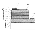
図1には、本発明の一実施の形態に係るMQWからなる窒化物半導体発光素子の層構造を表す断面図を示す。
【0043】
この発光素子は、サファイアからなる基板1の上に、GaNからなるバッファ層2と、GaNからなる第1のn型クラッド層3と、AlGaNからなる第2のn型クラッド層4と、InGaNからなる井戸層5およびGaNからなる障壁層6を交互に成長させたMQW層(5〜10)と、AlGaNからなるp型クラッド層11とが順に積層されている。また、p型クラッド層11の表面には透光性電極12、p側電極13が順に形成され、第1のn型クラッド層3の表面にはn側電極14が形成されている。
【0044】
この発光素子におけるMQWは、MOCVD法を用いて、以下の方法によって作製される。
【0045】
まず、反応管内に十分洗浄したサファイアからなる基板1を装入し、反応管内に窒素と水素を流しながら、基板1を約1050℃で10分間加熱し、基板1の表面のクリ−ニングを行う。
【0046】
次に、基板1の温度を550℃まで降下させ、窒素、TMG、アンモニアをそれぞれ流してGaNバッファ層2を基板1の上に形成する。バッファ層2を形成後は、窒素とアンモニアをそれぞれを流しながら基板1の温度を1050℃まで昇温し、この温度下おいて、窒素、水素、TMG、アンモニア、SiH4をそれぞれ流して第1のn型GaNクラッド層3を形成する。第1のn型GaNクラッド層3を形成後は、引き続き1050℃において、窒素、水素、TMG、TMA、アンモニアをそれぞれ流して第2のn型AlGaNクラッド層4を形成する。
【0047】
次に、水素、TMG、TMAの各供給を止めて、基板1の温度を750℃まで下げ、窒素、TMG、TMI、アンモニアをそれぞれ流して、InGaNからなる井戸層5を形成する。
【0048】
その後、TMIの供給のみを止めて、引き続き、基板温度を750℃から1050℃まで昇温しながら障壁層Aを形成し、更に1050℃において、窒素、水素、 TMG、アンモニアをそれぞれ流しながら、障壁層Bを形成し、障壁層Aと障壁層Bを合わせて障壁層6とする。次に、水素とTMGの供給を止め、基板1の温度を750℃まで下げる。あとは、井戸層5と障壁層6と同様の手順を繰返し、井戸層7、障壁層8、井戸層9、障壁層10を順次積層し、MQWを形成する。この方法によれば、井戸層の分解が抑制できると同時に、障壁層の結晶性を高めることができる。
【0049】
本発明者らの知見によれば、障壁層Bの成長速度は障壁層Aの成長速度より大きくすることが望ましい。具体的には、障壁層Aの成長速度は0.01μm/h〜0.5μm/hであるのに対し、障壁層Bの成長速度は0.1μm/h〜10μm/hであることが好ましい。障壁層Bの成長速度が0.1μm/hよりも小さいとMQWの形成に時間がかかり過ぎるし、10μm/hより大きいと障壁層Bの結晶性が悪化する。障壁層の膜厚は井戸層に比較して厚く形成する必要があり、特に、障壁層Bの成長時に、障壁層Aよりも高い成長速度とすることによって、高温(概略一定温度)での成長速度が大きくなるので、障壁層の結晶性が向上すると同時に、障壁層を厚くする場合や、MQWの周期数を増やす場合に、成長時間を従来よりも短縮することができ、MQWからなる窒化物半導体の製造コストを低減できる。
【0050】
次に、障壁層Bの成長時の雰囲気の水素濃度は障壁層Aの成長時の雰囲気の水素濃度よりも高くすることが望ましい。具体的には、障壁層Aの成長時の雰囲気の水素濃度が0%〜5%であるのに対し、障壁層Bの成長時の雰囲気の水素濃度は5%〜70%が好ましい。ここで、水素濃度は水素ガスの容量比である。障壁層Bの成長時の雰囲気の水素濃度が5%より低い場合は、障壁層Bの結晶性が悪化するし、70%以上では、基板面内での膜厚等の均一性が悪化する。
【0051】
障壁層Aにおいては、井戸層の分解を抑制することが重要となるため、障壁層の成長時の雰囲気の水素濃度は低い方が、井戸層の分解が抑えられる。これに対し、障壁層Bは障壁層の結晶性を向上させることが重要となるため、高温(1050℃)で障壁層Aよりも成長時の雰囲気の水素濃度を高めることにより、成長表面でのマイグレ−ションを促進し、障壁層の結晶性を向上させることができる。
【0052】
次に、障壁層Bの成長時のV/III比は障壁層Aの成長時のV/III比よりも小さくすることが望ましい。具体的には、障壁層AのV/III比が1×104〜2×105であるのに対し、障壁層BのV/III比は5×102〜1×104が好ましい。障壁層BのV/III比が5×102よりも小さい場合は、障壁層Bの成長時に成長表面での窒素分圧不足によりピット等が発生しやすくなり、1×104以上になると成長表面の極性が窒素面となることにより障壁層Bの表面モフォロギーが悪化するようになる。
【0053】
次に、MQWの井戸層はInxGa1-xN(0<x<y)、障壁層はInyAlzGa1-y-zN(0≦y<1、0≦z<1、0≦y+z<1、x>y)とすることが望ましい。井戸層の成長直後に昇温しながら障壁層の一部を成長させるので、障壁層の材料を窒化物半導体、すなわちInyAlzGa1-y-zN(0≦y<1、0≦z<1、0≦y+z<1、x>y)とすることにより、井戸層の劣化が抑制されると同時に、障壁層の結晶性も高めることができるため、発光特性のすぐれたMQWからなる窒化物半導体を作製することができる。
【0054】
また、障壁層をGaNとすれば、障壁層の結晶性をさらに高めることができる。
【0055】
次に、基板温度については、井戸層は500℃〜900℃の範囲が望ましい。井戸層では、成長時においても分解が発生するので、900℃よりも高いとInGaNの分解が促進されて井戸層がほとんど成長しなくなり、500℃よりも低いと井戸層の結晶性が悪くなる。一方、昇温後の基板温度は800℃〜1200℃が望ましい。基板温度がより高い方が障壁層の結晶性は向上するが1200℃よりも高いと、ウェハーの表面荒れが発生するし、MOCVD装置の基板加熱源への負荷も大きくなり、好ましくない。また、基板温度が800℃よりも低いと、十分な結晶性をもつ障壁層が成長できない。
【0056】
次に、少なくとも障壁層Aの成長開始時のGa原料供給量は井戸層のGa原料供給量より少なくすることが望ましい。具体的には、井戸層成長時のTMG供給量が2μmol/分〜10μmol/分であるのに対し、障壁層Aの成長開始時のTMG供給量は0.4μmol/分〜4μmol/分が好ましい。障壁層Aの成長開始時のTMG供給量が0.4μmol/分よりも小さいと、障壁層Aを成長させる際、井戸層の分解を抑制することが困難となるし、4μmol/分よりも大きいと、障壁層Aの結晶性が悪化する。これは、障壁層AのTMG供給量を増やすと井戸層の分解は抑制され易くなるが、障壁層を低温で比較的速い成長速度で成長させることになるので、障壁層の結晶性がより悪化するためである。
【0057】
また、障壁層Aを基板温度を昇温させながら成長させる際に、基板温度の上昇に伴い、障壁層Aの成長速度を徐々に速めることもできる。この場合、Ga原料供給量は障壁層Aの成長開始初期は0.4μmol/分〜4μmol/分で、障壁層Aの成長終了直前では20μmol/分〜100μmol/分とすることができる。
【0058】
次に、井戸層を成長させる基板温度よりも高い基板温度で障壁層を成長した後、基板温度を井戸層を成長させる温度まで降温する際にも、少なくとも障壁層の一部を成長させることが、成長時間短縮の点で望ましい。前記降温時は井戸層成長後の昇温時に比較して井戸層への影響(結晶性の劣化)が少なくなるため、前記昇温時に比較して、成長速度を早くできるという利点がある。なお、高温の方が障壁層の結晶性がよいことは明らかなため、降温開始時の成長速度を早くし、温度の低下と共に徐々に成長速度を遅くすることも可能である。これにより、MQWの成長時間が短縮され、MQW発光層からなる窒化物半導体の製造コストを低減することできる。
【0059】
次に、基板はサファイアやSiCを用い、その上にバッファ層を積層し、さらに窒化物半導体からなる下地層を成長させることにより、高い結晶性をもつ下地層を成長させることができ、その上に成長させるMQWの品質が向上するため、MQWからなる窒化物半導体の発光効率を高めることができる。
【0060】
さらに、基板を窒化物半導体基板とすることができる。これにより、基板と下地層の格子定数差および熱膨脹係数差を従来よりも減らすことができ、窒化物半導体からなる下地層の結晶性をさらに高めることができる。これにより、前記下地層の上に成長させるMQWの品質がさらに向上するため、MQWからなる窒化物半導体の発光効率を高めることができる。
【0061】
また、MQWの下地層は一般的にGaNが用いられており、基板をGaNとすることにより、基板と下地層が同一材料となり、さらに結晶性にすぐれた下地層を成長できるため、その上に積層するMQWの品質をさらに高めることができ、MQWからなる窒化物半導体の発光効率を高めることができる。
【0062】
上記以外にもサファイア、SiC、GaAs等の基板上に厚膜のGaNを積層したGaN積層基板を用いてもよいし、前記のGaN積層基板や前記の窒化物半導体基板上にSiO2等のマスクでパタ−ニングしたものを基板として用いても同様にMQWからなる窒化物半導体の発光効率を高めることができる。
【0063】
【実施例】
以下、本発明のMQW構造をもつ窒化ガリウム系化合物半導体の製造方法の具体例について図面を参照しながら説明する。
【0064】
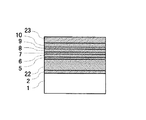
(実施例1)
図2は、本発明の実施例1に係るMQWからなる窒化物半導体の層構造を表す断面図であり、図3は、本発明の実施例1に係るMQWからなる窒化物半導体の成長プロファイル(基板温度、成長速度、水素濃度、アンモニア流量)を示す図である。
【0065】
先ず、表面を鏡面に仕上げられたサファイアの基板1をMOCVD装置の反応管内の基板ホルダーに載置した後、基板1の温度を1000℃に保ち、窒素を5リットル/分、水素を5リットル/分、で流しながら基板1を10分間加熱することにより、基板1の表面に付着している有機物等の汚れや水分を取り除いた。
【0066】
次に、基板1の温度を550℃にまで降下させ、キャリアガスとして窒素を16リットル/分、アンモニアを4リットル/分、TMGを40μmol/分、で供給して、GaNからなるバッファ層2を25nmの厚さで成長させた。
【0067】
次に、TMGの供給のみを止めて基板1の温度を1050℃まで昇温させた後、キャリアガスとして窒素と水素を各々13リットル/分と3リットル/分で流しながら、アンモニアを4リットル/分、TMGを80μmol/分、で供給して、アンドープのGaNからなる下地層22を2μmの厚さで成長させた。
【0068】
下地層22を成長後、TMGの供給を止め、基板1の温度を750℃にまで降下させ、この温度に維持して、キャリアガスとして窒素を14リットル/分、アンモニアを6リットル/分、TMGを4μmol/分、TMIを5μmol/分、で供給して、アンドープのIn0.15Ga0.85Nからなる量子井戸構造の井戸層5を2nmの厚さで成長させた。
【0069】
井戸層5を成長後、TMIの供給を止め、キャリアガスとして窒素を14リットル/分、アンモニアを6リットル/分、TMGを2μmol/分で供給して、基板1の温度を1050℃に向けて昇温させながら、引き続きアンドープのGaN(障壁層A)を3nmの厚さで成長させ、基板1の温度が1050℃に達したら、キャリアガスとして窒素と水素を各々15リットル/分と3リットル/分で流しながら、アンモニアを2リットル/分、TMGを40μmol/分、で供給して、引き続きアンドープのGaN(障壁層B)を12nmの厚さで成長させた。こうしてアンドープのGaNからなる厚さ15nmの障壁層6を形成した。そして、キャリアガスとして窒素を19リットル/分、アンモニアを1リットル/分で流しながら、基板温度を再度750℃にまで降下させ、井戸層5と障壁層6の製法と同様の手順を繰り返すことにより、井戸層7、障壁層8、井戸層9、障壁層10を形成した。
【0070】
障壁層10を成長後は、基板1の温度を1050℃に保ち、引き続き、キャリアガスとして窒素と水素を各々13リットル/分と3リットル/分で流しながら、アンモニアを4リットル/分、TMGを80μmol/分、で供給して、アンドープのGaNからなるキャップ層23を100nm成長させた。
【0071】
このようにして、3層の井戸層からなるMQWを形成し、試料1とした。
【0072】
(比較例1)
上記の実施例1の製造方法の中のMQWを形成する工程において、下地層22を成長後、TMGの供給を止め、基板1の温度を750℃にまで降下させ、750℃において、キャリアガスとして窒素を14リットル/分、アンモニアを6リットル/分、TMGを4μmol/分、TMIを5μmol/分、で供給して、アンドープのIn0.15Ga0.85Nからなる単一量子井戸構造の井戸層5を2nmの厚さで成長させた。次に、基板温度は750℃のまま保持し、キャリアガスとして窒素を14リットル/分で流しながら、アンモニアを6リットル/分、TMGを2μmol/分で供給してアンドープのGaNを15nmの厚さで成長させ、障壁層6とした。
【0073】
以降、井戸層5と障壁層6の製法と同様の手順を繰り返すことにより、井戸層7、障壁層8、井戸層9、障壁層10を順次に形成した。
【0074】
次に、キャリアガスとして窒素を14リットル/分、アンモニアを1リットル/分で流しながら、基板1の温度を1050℃まで昇温させ、昇温後はキャリアガスとして窒素と水素を各々13リットル/分と3リットル/分で流しながら、アンモニアを4リットル/分、TMGを80μmol/分、で供給してキャップ層23を100nm積層した。
【0075】
このようにして、実施例1と同一構造の3層の井戸層からなるMQWを形成し、試料2とした。
【0076】
まず、実施例1の試料1と、比較例1の試料2についてフォトルミネッセンス(PL)測定装置を用いて光学特性の比較を行なった。PL測定装置に用いた励起光はHe−Cdレーザ(波長325nm)で、励起強度は10mWとした。
【0077】
図4は、試料1および試料2のフォトルミネッセンススペクトルを示す図である。試料1のPLスペクトル31は試料2のPLスペクトル32に比較して約4倍の発光強度であった。これは、試料1の方がより高い温度で障壁層を成長したので、MQWの結晶性が向上したためと考えられる。また、昇温後(1050℃の一定温度)に障壁層の成長速度を20倍に高めることにより、試料1のMQWの成長時間が試料2よりも約30分間短縮できた。
【0078】
(実施例2)
本発明の第2の実施例である窒化物半導体を用いた発光素子の製造方法について図1を参照しながら説明する。
【0079】
先ず、表面を鏡面に仕上げられたサファイアの基板1をMOCVD装置の反応管内の基板ホルダーに載置した後、基板1の温度を1000℃に保ち、窒素を5リットル/分、水素を5リットル/分、で流しながら基板を10分間加熱することにより、基板1の表面に付着している有機物等の汚れや水分を取り除いた。
【0080】
次に、基板1の温度を550℃にまで降下させ、キャリアガスとして窒素を16リットル/分で流しながら、アンモニアを4リットル/分、TMGを40μmol/分、で供給して、アンドープのGaNからなるバッファ層2を25nmの厚さで成長させた。
【0081】
次に、TMGの供給を止めて1050℃まで昇温させた後、キャリアガスとして窒素と水素を各々13リットル/分と3リットル/分で流しながら、アンモニアを4リットル/分、TMGを80μmol/分、10ppm希釈のSiH4を10cc/分、で供給して、SiをドープしたGaNからなる第1のn型クラッド層3を2μmの厚さで成長させた。
【0082】
第1のn型クラッド層3を成長後、基板1の温度を1050℃に保ち、キャリアガスとして窒素と水素を各々15リットル/分と3リットル/分で流しながら、アンモニアを2リットル/分、TMGを40μmol/分、TMAを3μmol/分、で供給して、アンドープのAl0.05Ga0.95Nからなる第2のn型クラッド層4を20nmの厚さで成長させた。
【0083】
第2のn型クラッド層4を成長後、TMGとSiH4の供給を止め、基板温度を750℃にまで降下させ、750℃において、キャリアガスとして窒素を14リットル/分で流しながら、アンモニアを6リットル/分、TMGを4μmol/分、TMIを5μmol/分、で供給して、アンドープのIn0.15Ga0.85Nからなる量子井戸構造の井戸層5を2nmの厚さで成長させた。
【0084】
井戸層5を成長後、TMIの供給を止め、キャリアガスとして窒素を14リットル/分、アンモニアを6リットル/分、TMGを2μmol/分で供給して、基板1の温度を1050℃に向けて昇温させながら、引き続きアンドープのGaN(障壁層A)を3nmの厚さで成長させ、基板1の温度が1050℃に達したら、キャリアガスとして窒素と水素を各々15リットル/分と3リットル/分で流しながら、アンモニアを2リットル/分、TMGを40μmol/分、で供給して、引き続きアンドープのGaN(障壁層B)を12nmの厚さで成長させた。こうしてアンドープのGaNからなる厚さ15nmの障壁層6を形成した。そして、キャリアガスとして窒素を19リットル/分、アンモニアを1リットル/分で流しながら、基板温度を再度750℃にまで降下させ、井戸層5と障壁層6の製法と同様の手順を繰り返すことにより、井戸層7、障壁層8、井戸層9、障壁層10を順に形成した。
【0085】
障壁層10を形成後は、基板1の温度を1050℃に保ち、引き続き、キャリアガスとして窒素と水素を各々15リットル/分と3リットル/分で流しながら、アンモニアを2リットル/分、TMGを40μmol/分、TMAを3μmol/分、Cp2Mgを0.4μmol/分、で供給して、MgをドープさせたAl0.05Ga0.95Nからなるp型クラッド層11を0.2μmの厚さで成長させた。
【0086】
p型クラッド層11を成長後、TMGとTMAとCp2Mgの供給を止め、窒素を18リットル/分、アンモニアを2リットル/分、で流しながら、基板の温度を室温程度にまで冷却させて、基板の上に窒化物半導体が積層されたウェハーを反応管から取り出した。
【0087】
尚、有機金属化合物であるTMGと、TMIと、TMAと、Cp2Mgはすべて水素キャリアガスによって気化することで、反応管に供給した。
【0088】
このようにして形成した窒化ガリウム系化合物半導体からなる積層構造に対して、別途アニールを施すことなく、その表面上に、蒸着法により、ニッケル(Ni)と金(Au)をそれぞれ5nmの厚さで全面に積層した後、フォトリソグラフィ法とウェットエッチング法により、透光性電極12を形成した。
【0089】
この後、透光性電極12と露出したp型クラッド層11の上にCVD法によりSiO2からなる絶縁膜(図示せず)を0.5μmの厚さで堆積させ、フォトリソグラフィ法と反応性イオンエッチング法により、透光性電極12を覆うと同時にp型クラッド層11の表面の一部を露出させる絶縁膜からなるマスクを形成した。
【0090】
次に、上記のマスクを用いて、塩素系ガスを用いた反応性イオンエッチング法により、露出させたp型クラッド層11の表面側から、p型クラッド層11とMQW層(5〜10)と第2のn型クラッド層4を約0.4μmの深さで除去して、第1のn型クラッド層3の表面を露出させた。
【0091】
上記の工程の後、一旦、絶縁膜をウェットエッチング法により除去して、蒸着法およびフォトリソグラフィ法により、透光性電極12の表面上の一部と、露出させた第1のn型クラッド層3の表面の一部とに、0.1μm厚のチタン(Ti)と0.5μm厚のAuを積層して、それぞれp側電極13とn側電極14とした。その後、プラズマCVD法とフォトリソグラフィ法により、透光性電極12の表面を被覆する0.2μm厚のSiO2からなる絶縁性膜(図示せず)を形成した。
【0092】
この後、サファイアの基板1の裏面を研磨して100μm程度にまで薄くし、スクライブによりチップ状に分離した。このチップを電極形成面側を上向きにしてステムに接着した後、チップのp側電極13とn側電極14をそれぞれステム上の電極にワイヤで結線し、その後樹脂モールドして発光素子を作製し、試料3とした。この発光素子を20mAの順方向電流で駆動したところ、ピーク波長470nmの青色で発光した。このときの発光出力は4mWであり、順方向動作電圧は3.8Vであった。
【0093】
(実施例3)
本発明の第3の実施例である窒化物半導体を用いた発光素子の製造方法について図面を参照しながら説明する。
【0094】
図5は本発明の実施例3に係るMQW構造をもつ窒化物半導体からなる発光素子の層構造を表す断面図である。
【0095】
実施例2に示したMQW構造をもつ窒化物半導体からなる発光素子において、基板が窒化物半導体の場合について試作し、発光出力を調べた。例として、窒化物半導体基板がGaNである発光素子を作製した。基板は、HVPE法(ハイドライド気相成長)により、サファイア基板上に100μm厚のGaNを積層した後、基板表面の凹凸を除去するために、ダイヤモンドスラリーを用いて深さ10μmの研磨を行なった。研磨後は、GaN表面に発生した機械加工によるダメージ層を除去し、最後にサファイア基板を除去してGaN基板21とした。GaN基板21は研磨時の潤滑油、ワックス等の有機物や不純物を除去するため、有機洗浄および超純水洗浄を実施し、乾燥後に、MOCVD装置の反応管内の基板ホルダーに載置した。
【0096】
まず、GaN基板21の温度を室温から直接1050℃まで昇温させた後、キャリアガスとして窒素と水素を各々13リットル/分と3リットル/分で流しながら、アンモニアを4リットル/分、TMGを80μmol/分、10ppm希釈のSiH4を10cc/分、で供給して、SiをドープしたGaNからなる第1のn型クラッド層3を2μmの厚さで成長させた。
【0097】
その後は、実施例2と同様の成長手順により、第2のn型クラッド層4、井戸層5、障壁層6、井戸層7、障壁層8、井戸層9、障壁層10、MgドープAlGaNクラッド層11を順次に積層し、電極プロセスとして透光性電極12、p側電極13、n側電極14を形成して発光素子を作製し、試料4とした。この発光素子を20mAの順方向電流で駆動したところ、ピーク波長470nmの青色で発光した。このときの発光出力は4mWであり、順方向動作電圧は3.4Vであった。この場合、発光出力は実施例2で示したサファイア基板を用いた発光素子(試料3)と同等レベルのものが得られている。これより、基板がGaNの場合、実施例2と同様に発光素子の発光効率が大幅に向上し、順方向動作電圧がさらに低減されることを確認した。
【0098】
なお、以上説明した実施の形態では主として発光ダイオードに適用した例を説明したが、本発明は発光ダイオードに限らず、窒化物半導体を用いた半導体レーザ等の各種の半導体素子に適用することも可能である。
【0099】
【発明の効果】
以上のように本発明によれば、多重量子井戸構造(MQW)からなる窒化物半導体において、井戸層成長直後に基板を昇温しながら障壁層を成長させることによって、井戸層の劣化を抑制すると同時に、障壁層の結晶性を向上させることができ、前記窒化物半導体からなる発光素子における発光効率を向上させることができるという優れた効果が得られる。
【0100】
また、障壁層を厚く形成したり、MQWの周期数を増やしたりする場合に、MQW発光層の形成時間を従来よりも短縮化することができ、窒化物半導体からなる発光素子の製造コストを低減することが可能となる。
【図面の簡単な説明】
【図1】本発明の一実施の形態に係るMQWからなる窒化物半導体発光素子の層構造を表す断面図
【図2】本発明の実施例1に係るMQWからなる窒化物半導体の層構造を表す断面図
【図3】本発明の実施例1に係るMQWからなる窒化物半導体の成長プロファイル(基板温度、成長速度、水素濃度、アンモニア流量)を示す図
【図4】試料1および試料2のフォトルミネッセンススペクトルを示す図
【図5】本発明の実施例3に係るMQW構造をもつ窒化物半導体からなる発光素子の層構造を表す断面図
【符号の説明】
1 基板
2 バッファ層
3 第1のn型クラッド層
4 第2のn型クラッド層
5、7、9 井戸層
6、8、10 障壁層
11 p型クラッド層
12 透光性電極
13 p側電極
14 n側電極
21 GaN基板
22 下地層
23 キャップ層
31 試料1のPL強度
32 試料2のPL強度[0001]
BACKGROUND OF THE INVENTION
The present invention relates to a method for manufacturing a nitride semiconductor used in an optical device such as a light emitting diode or a semiconductor laser diode.
[0002]
[Prior art]
A nitride semiconductor represented by AlGaInN containing Al, Ga, In or the like as a Group III element and N or the like as a
[0003]
In the manufacture of light-emitting elements using nitride semiconductors, it is a mainstream in recent years to grow nitride semiconductor thin film crystals by metal organic chemical vapor deposition (MOCVD). In this method, an organometallic compound gas (trimethylgallium (hereinafter abbreviated as “TMG”), trimethylaluminum (hereinafter, abbreviated as “TMG”) is used as a group III element source gas in a reaction tube provided with a substrate made of sapphire, SiC, GaN, or the like. Abbreviated as “TMA”), trimethylindium (hereinafter abbreviated as “TMI”), etc., and ammonia, hydrazine or the like as the source gas of the group V element, and the substrate temperature is about 700 ° C. to 1100 ° C. The n-type layer, the light-emitting layer, and the p-type layer are grown on the substrate by stacking these layers. When growing the n-type layer, monosilane (SiH) is used as the n-type impurity source gas. Four ) And germane (GeH Four ) Or the like as a p-type impurity source gas during the growth of the p-type layer. 2 Mg) or dimethylzinc (Zn (CH Three ) 2 ) Etc. while growing simultaneously with the source gas of the group III element.
[0004]
Then, after this growth and formation, an n-side electrode and a p-side electrode are formed on the surface of the n-type layer and the surface of the p-type layer, respectively, and separated into chips, whereby a light emitting element can be obtained.
[0005]
The light emitting layer uses InGaN whose In composition is adjusted so that the desired light emission wavelength is obtained, and a double hetero structure in which this is sandwiched by a clad layer having a band gap energy larger than that of the light emitting layer, and the light emitting layer has a quantum size effect. A quantum well structure formed of such a thin layer is generally used, but recently, a quantum well structure having a high luminous efficiency has become the mainstream.
[0006]
This quantum well structure is formed by sandwiching a layer having a smaller band gap energy called a well layer between layers having a larger band gap energy than the well layer.
[0007]
In addition, a multiple quantum well (MQW) having a higher light emission efficiency than a single quantum well having a single well layer is made of In x Ga 1-x A well layer composed of N (0 <x <1) and In y Al z Ga 1-yz N (0 ≦ y <1, 0 ≦ z <1, 0 ≦ y + z <1, x> y) is formed by alternately laminating barrier layers, and the following three methods for manufacturing a conventional MQW are provided. It is divided roughly into.
[0008]
The first conventional technique is disclosed in Japanese Patent Laid-Open No. 10-12922. This is a nitride semiconductor light emitting device made of MQW in which barrier layers made of AlGaN and well layers made of InGaN are alternately stacked, and a buffer layer made of AlN and Si are doped on a sapphire substrate using an MOCVD apparatus. After the stacked GaN layers are sequentially stacked, a light emitting layer made of MQW is stacked, and a cladding layer and a contact layer doped with Mg are sequentially stacked thereon.
[0009]
Regarding the growth method of MQW in this light emitting device, first, the substrate temperature is maintained at 1100 ° C. 2 Or H 2 Introducing ammonia, TMG, TMA, Al 0.05 Ga 0.95 A barrier layer having a thickness of 50 mm made of N is formed, and subsequently the substrate temperature is lowered to 800 ° C. and maintained. 2 Or H 2 , Ammonia, TMG, TMI, and silicon and zinc doped In 0.20 Ga 0.80 A well layer made of N and having a thickness of 50 mm is formed. Then, the barrier layer and the well layer are alternately grown to form a light emitting layer made of MQW having a total thickness of 0.055 μm. At this time, the barrier layer has the same growth rate as the well layer.
[0010]
In this structure, the MQW made of the strained superlattice of the well layer and the barrier layer is used for the light emitting layer, so that a high-quality crystal with few dislocations can be obtained, and the light emission efficiency of the nitride semiconductor light emitting device is improved. It is shown.
[0011]
The second prior art is disclosed in Japanese Patent Laid-Open No. 10-135514. This is because the substrate temperature is maintained at 900 ° C. in the MQW growth method of the light emitting element, and N 2 Then, TMG and ammonia are introduced to form a barrier layer made of GaN having a thickness of 3.5 nm. Next, the substrate temperature is maintained at 750 ° C., and in addition to N2, TMG, and ammonia, TMI is introduced to form a 3.5 nm thick In 0.16 Ga 0.84 A well layer made of N is formed. Then, the barrier layers and the well layers are alternately grown to form five barrier layers and well layers. Furthermore, the substrate temperature is maintained at 900 ° C., and the uppermost barrier layer made of 14 nm of GaN is formed on the fifth quantum well layer. At this time, the barrier layer has the same growth rate as the well layer.
[0012]
This structure prevents the wavelength shift of the emitted light by making the layer on the side in contact with the Si-doped GaN layer and the Mg-doped cladding layer a barrier layer and making the thickness of each barrier layer uniform. It has been shown that it can.
A third conventional technique is disclosed in Japanese Patent Laid-Open No. 11-224972. This is because the substrate temperature is kept at 750 ° C. in the MQW growth method of the light emitting element, and the InW 0.2 Ga 0.8 A well layer made of N is formed with a thickness of 25 mm. Next, at the same substrate temperature only by changing the molar ratio of TMI, In 0.01 Ga 0.95 A barrier layer made of N is formed to a thickness of 50 mm. This operation is repeated 13 times. Finally, a well layer is formed, and an active layer having a multiple quantum well structure with a total film thickness of 0.1 μm is formed. At this time, the barrier layer has the same growth rate as the well layer.
[0013]
In this example, the barrier layer is formed as InGaN having a larger band gap than the well layer, and when the barrier layer made of InGaN is formed on the well layer, the barrier layer made of InGaN is compared with GaN or AlGaN crystal. Since the crystal is soft, it is difficult for cracks to occur in the cladding layer above the MQW, and the cladding layer can be thickened, which is particularly effective for improving the quality of a semiconductor laser made of a nitride semiconductor. It is shown.
[0014]
Further, when the barrier layer is also InGaN, the well layer and the barrier layer can be grown at the same temperature, so that the decomposition of the well layer formed earlier can be suppressed. It has been shown that the MQW growth time can be shortened because the layers can be grown continuously.
[0015]
[Problems to be solved by the invention]
However, the MQW formation method as described above has the following problems.
[0016]
First, in the first conventional technique, after the well layer made of InGaN is grown, the well layer is decomposed in the process of raising the temperature to the substrate temperature (1100 ° C.) for growing the barrier layer made of AlGaN. It is difficult to grow a well layer having excellent crystallinity.
[0017]
Next, also in the second conventional technique, at least the well layer is decomposed in the process of growing the well layer made of InGaN to the substrate temperature (900 ° C.) for growing the barrier layer made of GaN. Therefore, it is difficult to grow a well layer with excellent crystallinity.
[0018]
On the other hand, in the third conventional technique, since the substrate temperature for growing the well layer and the barrier layer is the same, the decomposition of the well layer is small. However, in MQW, in order for the barrier layer to function sufficiently, the barrier layer needs to have a sufficiently low In composition compared to the well layer. In this example, the In composition of the barrier layer is 0.01, and it is difficult to control such a low In composition.
[0019]
The InGaN of the barrier layer is substantially a crystal close to GaN. As a result, the barrier layer, which is a crystal close to GaN, is grown at the same substrate temperature (750 ° C.) as that of the well layer. Therefore, the crystallinity of the barrier layer is compared with that in the case of growing near 1100 ° C. in the
[0020]
Thus, in the conventional MQW manufacturing method, in order to improve the crystallinity of the barrier layer, when the substrate temperature for growing the barrier layer is raised above the substrate temperature for growing the well layer, the well layer deteriorates, When the well layer is grown at the same substrate temperature, there is a problem that the crystallinity of the barrier layer becomes insufficient and the quality of MQW is lowered.
[0021]
In order to produce a high-quality MQW, the barrier layer needs to be formed thicker than the well layer. As is common to the three conventional techniques, in the method of growing the barrier layer and the well layer at the same growth rate, the growth time becomes longer when the barrier layer is thickened or the number of MQW cycles is increased. In addition to the increase in the manufacturing cost, the crystallinity of MQW is reduced.
[0022]
The problems to be solved in the present invention are to provide a method of manufacturing MQW with improved light emission efficiency by suppressing deterioration of the well layer and improving the crystallinity of the barrier layer, and shortening the formation time of MQW It is an object to provide a method for manufacturing a light-emitting element made of a nitride semiconductor whose manufacturing cost is reduced by the manufacturing process.
[0023]
[Means for Solving the Problems]
The present inventors diligently studied the manufacturing method of MQW (in particular, the substrate temperature, the growth rate, the hydrogen concentration in the atmosphere, and the V / III ratio). As a result, after the whole well is grown at a substrate temperature suitable for the growth of the well layer, a part of the barrier layer (hereinafter referred to as “barrier layer A”) is grown while the temperature of the substrate is raised, and further increased. After a portion of the barrier layer is grown at a substantially constant substrate temperature after heating (hereinafter referred to as “barrier layer B”), the substrate temperature is lowered to a temperature at which the well layer is grown, and the well layer is grown. It has been found that an MQW light emitting layer having excellent crystallinity and high light emission efficiency can be formed by repeating the steps.
[0024]
Next, when the barrier layer B is grown, the hydrogen concentration in the atmosphere is set higher than when the barrier layer A is grown, and the V / III ratio is set higher than that when the barrier layer A is grown. It has been found that the crystallinity of layer B can be improved.
[0025]
Further, when the barrier layer B is grown, the barrier layer B is grown at a growth rate higher than that of the well layer and the barrier layer A, and after the barrier layer B is grown, the temperature is lowered to the substrate temperature at which the well layer is grown. It has been found that by adding a process for growing at least a part of the barrier layer, the MQW formation time can be further shortened even when the barrier layer is thick or the number of periods of the MQW is large.
[0026]
According to such a configuration, when the MQW is formed, decomposition of the well layer can be suppressed, and at the same time, the crystallinity of the barrier layer can be improved, and an MQW light emitting layer with high luminous efficiency can be manufactured. Become. In addition, since the formation time of the MQW light emitting layer can be shortened, the manufacturing cost of the light emitting element made of a nitride semiconductor can be reduced.
[0027]
DETAILED DESCRIPTION OF THE INVENTION
First application The invention has a nitride structure having a multiple quantum well structure in which a well layer made of a nitride semiconductor and a barrier layer made of a nitride semiconductor having a band gap energy larger than that of the well layer are alternately stacked on a substrate. A method of manufacturing a semiconductor, comprising: a first step of growing the well layer at a first substrate temperature; and a second substrate temperature higher than the first substrate temperature from the first substrate temperature. A multiple quantum well is formed by sequentially repeating a second step of growing the barrier layer while raising the temperature and a third step of lowering the temperature from the second substrate temperature to the first substrate temperature. This is a method for manufacturing a nitride semiconductor.
[0028]
In this method, since the barrier layer is grown while raising the temperature immediately after the growth of the well layer, it is possible to suppress the decomposition of the well layer made of InGaN at the time of raising the temperature, and to improve the crystallinity of the barrier layer. Has an effect.
[0029]
Second application In the invention, after the barrier layer is grown in the second step, the barrier layer is further grown at a substrate temperature at which the second substrate temperature is kept substantially constant before the third step. Providing a fourth step. Nitride semiconductor features In this manufacturing method, since a part of the barrier layer is grown in a state where the substrate temperature is maintained higher than the substrate temperature at which the well layer is grown, the crystallinity of the barrier layer can be further enhanced.
[0030]
Third application In the invention, the growth rate in at least a part of the growth of the barrier layer in the fourth step is higher than the growth rate of the barrier layer in the second step. Nitride semiconductor features In this manufacturing method, a barrier layer relatively thicker than the well layer and an MQW having a large number of cycles can be grown in a short time, and the total MQW growth time can be shortened. The cost can be reduced.
[0031]
Application No. 4 According to the present invention, the hydrogen concentration in the atmosphere in at least part of the growth of the barrier layer in the fourth step is greater than the hydrogen concentration in the atmosphere during the growth of the barrier layer in the second step. Nitride semiconductor features In this manufacturing method, by increasing the hydrogen concentration in the fourth step, the migration of atoms on the substrate surface is promoted, and the crystallinity of the barrier layer can be further increased.
[0032]
Application No. 5 In the invention, the ratio of the Group V material supply amount to the Group III material supply amount (hereinafter referred to as the V / III ratio) in at least a part of the growth of the barrier layer in the fourth step is the second step. Less than the V / III ratio during the growth of the barrier layer in Nitride semiconductor features In the manufacturing method, when the barrier layer B is grown, the supply amount of ammonia can be significantly reduced without deteriorating the crystallinity of the barrier layer B, and the manufacturing cost of the nitride semiconductor made of MQW can be reduced. Have
[0033]
Application No. 6 In the present invention, the well layer is In x Ga 1-x N (where 0 <x <1), and the barrier layer is In y Al z Ga 1-yz N (where 0 ≦ y <1, 0 ≦ z <1, 0 ≦ y + z <1, x> y). Nitride semiconductor features In this manufacturing method, the nitride semiconductor material constituting the well layer and the barrier layer is limited to the above-described material, so that the MQW can be improved in quality and the nitride semiconductor made of MQW having excellent optical characteristics. It has the effect | action that can be produced.
[0034]
Application No. 7 According to the present invention, the barrier layer is GaN. Nitride semiconductor features This method has the effect that the crystallinity of the barrier layer can be further increased, and a nitride semiconductor made of MQW having excellent optical properties can be produced.
[0035]
Application No. 8 According to the invention, the first substrate temperature is 500 ° C. to 900 ° C., and the second substrate temperature is 800 ° C. to 1200 ° C. Nitride semiconductor features In this manufacturing method, the first substrate temperature and the second substrate temperature are limited to the above ranges, whereby a well layer and a barrier layer with excellent crystallinity can be produced.
[0036]
Application No. 9 According to the present invention, the Ga source supply amount at the start of growth of the barrier layer is less than the Ga source supply amount at the time of growth of the well layer. Nitride semiconductor features This method has the effect of suppressing the deterioration of the well layer and at the same time improving the crystallinity of the barrier layer.
[0037]
Application No. 10 According to the present invention, the barrier layer is grown in at least a part of the third step. Nitride semiconductor features By growing a part of the barrier layer even when the temperature is lowered, the MQW formation time can be shortened even when the barrier layer is thickened or the number of MQW cycles is increased. It has the effect | action that the manufacturing cost of the nitride semiconductor which consists of can be reduced.
[0038]
Application No. 11 In the invention, the substrate includes sapphire or SiC, a buffer layer including a nitride semiconductor is formed on the substrate at a substrate temperature lower than the first substrate temperature, and the nitride semiconductor is formed on the buffer layer. And forming the multiple quantum well on the underlayer. Nitride semiconductor features In this manufacturing method, an underlying layer having high crystallinity can be produced, and the quality of MQW grown thereon can be improved, so that the luminous efficiency of a nitride semiconductor light emitting device having a light emitting layer made of MQW can be increased. It has the action.
[0039]
Application No. 12 In the invention, the substrate includes a nitride semiconductor, a base layer including the nitride semiconductor is formed on the substrate, and the multiple quantum well is formed on the base layer. Nitride semiconductor features In this manufacturing method, an underlayer having higher crystallinity can be produced, and the quality of MQW grown thereon can be improved, so that the light emission efficiency of a nitride semiconductor light emitting device having a light emitting layer made of MQW can be improved. Has the effect of being able to.
[0040]
Application No. 13 According to the invention, the substrate is GaN. Nitride semiconductor features Since the substrate and the underlayer are made of the same material, an underlayer having higher crystallinity can be produced, and the quality of MQW grown on the underlayer can be improved, so that a light emitting layer made of MQW is provided. It has the effect | action that the luminous efficiency of the nitride semiconductor light-emitting device can be improved.
[0041]
Hereinafter, specific examples of embodiments of the present invention will be described with reference to the drawings.
[0042]
FIG. 1 is a cross-sectional view showing the layer structure of a nitride semiconductor light emitting device made of MQW according to an embodiment of the present invention.
[0043]
The light-emitting element includes a
[0044]
The MQW in this light emitting element is manufactured by the following method using the MOCVD method.
[0045]
First, a sufficiently cleaned
[0046]
Next, the temperature of the
[0047]
Next, supply of hydrogen, TMG, and TMA is stopped, the temperature of the
[0048]
Thereafter, only the supply of TMI is stopped, and subsequently the barrier layer A is formed while raising the substrate temperature from 750 ° C. to 1050 ° C., and further at 1050 ° C., while flowing nitrogen, hydrogen, TMG, and ammonia, respectively, Layer B is formed, and barrier layer A and barrier layer B are combined to form
[0049]
According to the knowledge of the present inventors, it is desirable that the growth rate of the barrier layer B is larger than the growth rate of the barrier layer A. Specifically, the growth rate of the barrier layer A is 0.01 μm / h to 0.5 μm / h, while the growth rate of the barrier layer B is preferably 0.1 μm / h to 10 μm / h. . If the growth rate of the barrier layer B is lower than 0.1 μm / h, it takes too much time to form MQW, and if it is higher than 10 μm / h, the crystallinity of the barrier layer B deteriorates. The barrier layer needs to be formed thicker than the well layer. In particular, when the barrier layer B is grown, the growth rate is higher than that of the barrier layer A, so that the barrier layer is grown at a high temperature (approximately constant temperature). Since the speed is increased, the crystallinity of the barrier layer is improved, and at the same time, when the barrier layer is thickened or when the number of MQW cycles is increased, the growth time can be shortened compared to the prior art. Semiconductor manufacturing costs can be reduced.
[0050]
Next, it is desirable that the hydrogen concentration in the atmosphere during the growth of the barrier layer B is higher than the hydrogen concentration in the atmosphere during the growth of the barrier layer A. Specifically, the hydrogen concentration in the atmosphere during the growth of the barrier layer A is 0% to 5%, while the hydrogen concentration in the atmosphere during the growth of the barrier layer B is preferably 5% to 70%. Here, the hydrogen concentration is a volume ratio of hydrogen gas. When the hydrogen concentration in the atmosphere during the growth of the barrier layer B is lower than 5%, the crystallinity of the barrier layer B is deteriorated, and when it is 70% or more, the uniformity of the film thickness in the substrate surface is deteriorated.
[0051]
In the barrier layer A, since it is important to suppress the decomposition of the well layer, the decomposition of the well layer is suppressed when the hydrogen concentration in the atmosphere during the growth of the barrier layer is low. On the other hand, since it is important for the barrier layer B to improve the crystallinity of the barrier layer, by increasing the hydrogen concentration in the growth atmosphere at a high temperature (1050 ° C.) than the barrier layer A, Migration can be promoted and the crystallinity of the barrier layer can be improved.
[0052]
Next, it is desirable that the V / III ratio during the growth of the barrier layer B is smaller than the V / III ratio during the growth of the barrier layer A. Specifically, the V / III ratio of the barrier layer A is 1 × 10. Four ~ 2x10 Five In contrast, the V / III ratio of the barrier layer B is 5 × 10 2 ~ 1x10 Four Is preferred. The V / III ratio of the barrier layer B is 5 × 10 2 When the barrier layer B is smaller than that, pits and the like are likely to occur due to insufficient nitrogen partial pressure on the growth surface during the growth of the barrier layer B. Four If it becomes above, the surface morphology of the barrier layer B will deteriorate by the polarity of the growth surface becoming a nitrogen surface.
[0053]
Next, the well layer of MQW is InxGa 1-x N (0 <x <y), the barrier layer is In y Al z Ga 1-yz N (0 ≦ y <1, 0 ≦ z <1, 0 ≦ y + z <1, x> y) is desirable. Since part of the barrier layer is grown while raising the temperature immediately after the growth of the well layer, the material of the barrier layer is a nitride semiconductor, that is, In y Al z Ga 1-yz By setting N (0 ≦ y <1, 0 ≦ z <1, 0 ≦ y + z <1, x> y), the deterioration of the well layer can be suppressed and the crystallinity of the barrier layer can be enhanced. Therefore, a nitride semiconductor made of MQW having excellent emission characteristics can be manufactured.
[0054]
If the barrier layer is GaN, the crystallinity of the barrier layer can be further increased.
[0055]
Next, as for the substrate temperature, the well layer is preferably in the range of 500 ° C to 900 ° C. In the well layer, decomposition occurs at the time of growth. If the temperature is higher than 900 ° C., the decomposition of InGaN is promoted so that the well layer hardly grows. On the other hand, the substrate temperature after the temperature rise is desirably 800 ° C. to 1200 ° C. When the substrate temperature is higher, the crystallinity of the barrier layer is improved. However, when the temperature is higher than 1200 ° C., the surface of the wafer is roughened, and the load on the substrate heating source of the MOCVD apparatus is increased, which is not preferable. If the substrate temperature is lower than 800 ° C., a barrier layer having sufficient crystallinity cannot be grown.
[0056]
Next, it is desirable that at least the Ga source supply amount at the start of growth of the barrier layer A be smaller than the Ga source supply amount of the well layer. Specifically, the TMG supply amount during the well layer growth is 2 μmol / min to 10 μmol / min, whereas the TMG supply amount at the start of the growth of the barrier layer A is preferably 0.4 μmol / min to 4 μmol / min. . If the TMG supply amount at the start of the growth of the barrier layer A is smaller than 0.4 μmol / min, it becomes difficult to suppress the decomposition of the well layer when growing the barrier layer A, and it is larger than 4 μmol / min. As a result, the crystallinity of the barrier layer A deteriorates. This is because when the TMG supply amount of the barrier layer A is increased, the decomposition of the well layer is easily suppressed, but the barrier layer is grown at a relatively low growth rate at a low temperature, so that the crystallinity of the barrier layer is further deteriorated. It is to do.
[0057]
Further, when growing the barrier layer A while raising the substrate temperature, the growth rate of the barrier layer A can be gradually increased as the substrate temperature rises. In this case, the Ga material supply amount is 0.4 μmol / min to 4 μmol / min at the beginning of growth of the barrier layer A, and can be 20 μmol / min to 100 μmol / min immediately before the growth of the barrier layer A is completed.
[0058]
Next, after growing the barrier layer at a substrate temperature higher than the substrate temperature at which the well layer is grown, at least part of the barrier layer can be grown when the substrate temperature is lowered to the temperature at which the well layer is grown. It is desirable in terms of shortening the growth time. When the temperature is lowered, the influence on the well layer (deterioration of crystallinity) is less than when the temperature is increased after the well layer is grown. Therefore, there is an advantage that the growth rate can be increased compared with the case where the temperature is raised. Since it is clear that the crystallinity of the barrier layer is better at higher temperatures, it is possible to increase the growth rate at the start of temperature decrease and gradually decrease the growth rate as the temperature decreases. Thereby, the growth time of MQW is shortened and the manufacturing cost of the nitride semiconductor which consists of a MQW light emitting layer can be reduced.
[0059]
Next, the substrate is made of sapphire or SiC, and a buffer layer is stacked thereon, and further, a base layer made of a nitride semiconductor is grown, whereby a base layer having high crystallinity can be grown. Since the quality of MQW to be grown is improved, the light emission efficiency of the nitride semiconductor made of MQW can be increased.
[0060]
Furthermore, the substrate can be a nitride semiconductor substrate. As a result, the lattice constant difference and the thermal expansion coefficient difference between the substrate and the underlayer can be reduced as compared with the conventional case, and the crystallinity of the underlayer made of a nitride semiconductor can be further enhanced. As a result, the quality of MQW grown on the underlying layer is further improved, so that the light emission efficiency of the nitride semiconductor made of MQW can be increased.
[0061]
In addition, GaN is generally used for the MQW underlayer, and by using GaN as the substrate, the substrate and the underlayer can be made of the same material, and further, an underlayer having excellent crystallinity can be grown thereon. The quality of the MQW to be stacked can be further improved, and the light emission efficiency of the nitride semiconductor made of MQW can be increased.
[0062]
In addition to the above, a GaN laminated substrate in which a thick GaN layer is laminated on a substrate of sapphire, SiC, GaAs or the like may be used, or SiO on the GaN laminated substrate or the nitride semiconductor substrate. 2 Even if a substrate patterned with a mask such as the above is used as the substrate, the light emission efficiency of the nitride semiconductor made of MQW can be similarly increased.
[0063]
【Example】
Hereinafter, a specific example of a method for producing a gallium nitride compound semiconductor having an MQW structure according to the present invention will be described with reference to the drawings.
[0064]
Example 1
FIG. 2 is a cross-sectional view showing a layer structure of a nitride semiconductor made of MQW according to Example 1 of the present invention, and FIG. 3 shows a growth profile of a nitride semiconductor made of MQW according to Example 1 of the present invention ( It is a figure which shows a substrate temperature, a growth rate, a hydrogen concentration, and an ammonia flow rate.
[0065]
First, a
[0066]
Next, the temperature of the
[0067]
Next, only the supply of TMG was stopped and the temperature of the
[0068]
After the
[0069]
After the
[0070]
After the growth of the
[0071]
In this manner, MQW composed of three well layers was formed and used as
[0072]
(Comparative Example 1)
In the process of forming MQW in the manufacturing method of the first embodiment, after the
[0073]
Thereafter, by repeating the same procedure as the manufacturing method of the
[0074]
Next, the temperature of the
[0075]
In this manner, MQW composed of three well layers having the same structure as that of Example 1 was formed and used as
[0076]
First, the optical characteristics of
[0077]
FIG. 4 is a diagram showing photoluminescence spectra of
[0078]
(Example 2)
A method for manufacturing a light-emitting device using a nitride semiconductor according to a second embodiment of the present invention will be described with reference to FIG.
[0079]
First, a
[0080]
Next, the temperature of the
[0081]
Next, after the supply of TMG was stopped and the temperature was raised to 1050 ° C., nitrogen and hydrogen were flowed at 13 liters / minute and 3 liters / minute respectively as carrier gases, while ammonia was 4 liters / minute and TMG was 80 μmol / minute. Min, 10ppm diluted SiH Four Was supplied at 10 cc / min, and the first n-
[0082]
After growing the first n-
[0083]
After growing the second n-
[0084]
After the
[0085]
After the
[0086]
After growing the p-
[0087]
In addition, TMG, TMI, TMA, and Cp which are organometallic compounds 2 All Mg was vaporized with a hydrogen carrier gas and supplied to the reaction tube.
[0088]
The laminated structure formed of the gallium nitride compound semiconductors formed in this manner has a thickness of 5 nm each for nickel (Ni) and gold (Au) on the surface thereof by vapor deposition without annealing. Then, the
[0089]
Thereafter,
[0090]
Next, the p-
[0091]
After the above steps, the insulating film is once removed by wet etching, and a part of the surface of the
[0092]
Thereafter, the back surface of the
[0093]
(Example 3)
A method for manufacturing a light-emitting device using a nitride semiconductor according to a third embodiment of the present invention will be described with reference to the drawings.
[0094]
FIG. 5 is a cross-sectional view showing a layer structure of a light emitting device made of a nitride semiconductor having an MQW structure according to Example 3 of the invention.
[0095]
In the light-emitting element made of a nitride semiconductor having the MQW structure shown in Example 2, the case where the substrate was a nitride semiconductor was prototyped and the light emission output was examined. As an example, a light emitting device in which the nitride semiconductor substrate is GaN was manufactured. The substrate was laminated by HVPE (hydride vapor phase growth) on a sapphire substrate with 100 μm thick GaN, and then polished to a depth of 10 μm using diamond slurry in order to remove irregularities on the substrate surface. After polishing, the damaged layer by machining generated on the GaN surface was removed, and finally the sapphire substrate was removed to obtain a
[0096]
First, after raising the temperature of the
[0097]
Thereafter, the second n-
[0098]
In the embodiment described above, an example mainly applied to a light emitting diode has been described. However, the present invention is not limited to a light emitting diode, but can be applied to various semiconductor elements such as a semiconductor laser using a nitride semiconductor. It is.
[0099]
【The invention's effect】
As described above, according to the present invention, in a nitride semiconductor having a multiple quantum well structure (MQW), by suppressing the deterioration of the well layer by growing the barrier layer while heating the substrate immediately after the well layer growth, At the same time, the crystallinity of the barrier layer can be improved, and an excellent effect can be obtained in that the light emission efficiency of the light emitting element made of the nitride semiconductor can be improved.
[0100]
In addition, when the barrier layer is formed thick or the number of MQW cycles is increased, the time for forming the MQW light emitting layer can be shortened compared to the conventional case, and the manufacturing cost of the light emitting element made of a nitride semiconductor can be reduced. It becomes possible to do.
[Brief description of the drawings]
FIG. 1 is a cross-sectional view showing a layer structure of a nitride semiconductor light emitting device made of MQW according to an embodiment of the present invention.
FIG. 2 is a sectional view showing a layer structure of a nitride semiconductor made of MQW according to Example 1 of the present invention.
FIG. 3 is a diagram showing a growth profile (substrate temperature, growth rate, hydrogen concentration, ammonia flow rate) of a nitride semiconductor composed of MQW according to Example 1 of the present invention.
FIG. 4 shows photoluminescence spectra of
FIG. 5 is a cross-sectional view showing a layer structure of a light-emitting element made of a nitride semiconductor having an MQW structure according to Example 3 of the invention.
[Explanation of symbols]
1 Substrate
2 Buffer layer
3 First n-type cladding layer
4 Second n-type cladding layer
5, 7, 9 well layer
6, 8, 10 Barrier layer
11 p-type cladding layer
12 Translucent electrode
13 p-side electrode
14 n-side electrode
21 GaN substrate
22 Underlayer
23 Cap layer
31 PL intensity of
32 PL intensity of
Claims (10)
Priority Applications (1)
| Application Number | Priority Date | Filing Date | Title |
|---|---|---|---|
| JP2000220454A JP4724901B2 (en) | 2000-07-21 | 2000-07-21 | Manufacturing method of nitride semiconductor |
Applications Claiming Priority (1)
| Application Number | Priority Date | Filing Date | Title |
|---|---|---|---|
| JP2000220454A JP4724901B2 (en) | 2000-07-21 | 2000-07-21 | Manufacturing method of nitride semiconductor |
Publications (3)
| Publication Number | Publication Date |
|---|---|
| JP2002043618A JP2002043618A (en) | 2002-02-08 |
| JP2002043618A5 JP2002043618A5 (en) | 2007-08-30 |
| JP4724901B2 true JP4724901B2 (en) | 2011-07-13 |
Family
ID=18715063
Family Applications (1)
| Application Number | Title | Priority Date | Filing Date |
|---|---|---|---|
| JP2000220454A Expired - Fee Related JP4724901B2 (en) | 2000-07-21 | 2000-07-21 | Manufacturing method of nitride semiconductor |
Country Status (1)
| Country | Link |
|---|---|
| JP (1) | JP4724901B2 (en) |
Cited By (1)
| Publication number | Priority date | Publication date | Assignee | Title |
|---|---|---|---|---|
| US9614121B1 (en) | 2016-01-27 | 2017-04-04 | Samsung Electronics Co., Ltd. | Method of fabricating semiconductor light emitting device |
Families Citing this family (17)
| Publication number | Priority date | Publication date | Assignee | Title |
|---|---|---|---|---|
| WO2003068699A1 (en) | 2002-02-15 | 2003-08-21 | Showa Denko K.K. | Group iii nitride semiconductor crystal, production method thereof and group iii nitride semiconductor epitaxial wafer |
| WO2005034253A1 (en) * | 2003-10-02 | 2005-04-14 | Showa Denko K.K. | Nitride semiconductor; light-emitting device, light-emitting diode, laser device and lamp using the semiconductor; and production methods thereof |
| JP2005129923A (en) * | 2003-10-02 | 2005-05-19 | Showa Denko Kk | Nitride semiconductor, light emitting element using it, light emitting diode, laser element, lamp, and manufacturing method for those |
| GB2407701A (en) | 2003-10-28 | 2005-05-04 | Sharp Kk | Manufacture of a semiconductor light-emitting device |
| JP4619647B2 (en) * | 2003-11-28 | 2011-01-26 | シャープ株式会社 | Method for manufacturing compound semiconductor device |
| JP4389723B2 (en) | 2004-02-17 | 2009-12-24 | 住友電気工業株式会社 | Method for forming a semiconductor device |
| JP4617922B2 (en) * | 2005-02-25 | 2011-01-26 | ソニー株式会社 | Manufacturing method of semiconductor device |
| JP2006332258A (en) | 2005-05-25 | 2006-12-07 | Matsushita Electric Ind Co Ltd | Nitride semiconductor device and its manufacturing method |
| KR100833434B1 (en) * | 2006-06-30 | 2008-05-29 | 주식회사 하이닉스반도체 | Method of manufacturing a flash memory device |
| JP2010021290A (en) * | 2008-07-09 | 2010-01-28 | Sumitomo Electric Ind Ltd | Method for manufacturing quantum well structure |
| JP4917585B2 (en) * | 2008-08-26 | 2012-04-18 | 住友電気工業株式会社 | Method for manufacturing nitride-based semiconductor optical device and method for manufacturing epitaxial wafer |
| CN102138227A (en) | 2008-08-29 | 2011-07-27 | 株式会社东芝 | Semiconductor device |
| JP2010123920A (en) | 2008-10-20 | 2010-06-03 | Sumitomo Electric Ind Ltd | Method for manufacturing nitride semiconductor light emitting element, and method for manufacturing epitaxial wafer |
| JP5394717B2 (en) * | 2008-12-15 | 2014-01-22 | 日本オクラロ株式会社 | Manufacturing method of nitride semiconductor optical device |
| JP4987994B2 (en) * | 2010-02-17 | 2012-08-01 | 株式会社東芝 | Method for crystal growth of nitride semiconductor |
| JP2015115343A (en) * | 2013-12-09 | 2015-06-22 | シャープ株式会社 | Method of manufacturing nitride semiconductor element |
| CN112768578A (en) * | 2021-02-07 | 2021-05-07 | 厦门乾照光电股份有限公司 | Semiconductor epitaxial structure, manufacturing method thereof and LED chip |
Citations (2)
| Publication number | Priority date | Publication date | Assignee | Title |
|---|---|---|---|---|
| JP2000049377A (en) * | 1998-07-30 | 2000-02-18 | Matsushita Electric Ind Co Ltd | Manufacture of gallium nitride compound semiconductor light-emitting device |
| JP2000077783A (en) * | 1998-08-27 | 2000-03-14 | Nec Corp | Growth method of indium-containing nitride semiconductor crystal |
-
2000
- 2000-07-21 JP JP2000220454A patent/JP4724901B2/en not_active Expired - Fee Related
Patent Citations (2)
| Publication number | Priority date | Publication date | Assignee | Title |
|---|---|---|---|---|
| JP2000049377A (en) * | 1998-07-30 | 2000-02-18 | Matsushita Electric Ind Co Ltd | Manufacture of gallium nitride compound semiconductor light-emitting device |
| JP2000077783A (en) * | 1998-08-27 | 2000-03-14 | Nec Corp | Growth method of indium-containing nitride semiconductor crystal |
Cited By (1)
| Publication number | Priority date | Publication date | Assignee | Title |
|---|---|---|---|---|
| US9614121B1 (en) | 2016-01-27 | 2017-04-04 | Samsung Electronics Co., Ltd. | Method of fabricating semiconductor light emitting device |
Also Published As
| Publication number | Publication date |
|---|---|
| JP2002043618A (en) | 2002-02-08 |
Similar Documents
| Publication | Publication Date | Title |
|---|---|---|
| JP3639789B2 (en) | Nitride semiconductor light emitting device | |
| US6455877B1 (en) | III-N compound semiconductor device | |
| JP4724901B2 (en) | Manufacturing method of nitride semiconductor | |
| US7998773B2 (en) | Method of growing semiconductor heterostructures based on gallium nitride | |
| JP4948720B2 (en) | Nitrogen compound semiconductor laminate, light emitting element, optical pickup system, and method for producing nitrogen compound semiconductor laminate. | |
| US5923950A (en) | Method of manufacturing a semiconductor light-emitting device | |
| US7646027B2 (en) | Group III nitride semiconductor stacked structure | |
| WO2011125449A1 (en) | Nitrogen compound semiconductor light emitting element and manufacturing method thereof | |
| JP2001160627A (en) | Group iii nitride compound semiconductor light emitting element | |
| JP2001160627A5 (en) | ||
| JPH06177423A (en) | Blue light emitting element | |
| JP2000232238A (en) | Nitride semiconductor light-emitting element and manufacture thereof | |
| KR100884288B1 (en) | Nitride semiconductor, light-emitting device, light-emitting diode, laser device and lamp using the semiconductor, and production methods thereof | |
| JP4734786B2 (en) | Gallium nitride compound semiconductor substrate and manufacturing method thereof | |
| JP5073624B2 (en) | Method for growing zinc oxide based semiconductor and method for manufacturing semiconductor light emitting device | |
| JP5401145B2 (en) | Method for producing group III nitride laminate | |
| US6365923B1 (en) | Nitride semiconductor light-emitting element and process for production thereof | |
| JP4214859B2 (en) | Method for manufacturing gallium nitride (GaN) substrate | |
| JP2010199236A (en) | Light emitting element producing method and light emitting element | |
| JP4103309B2 (en) | Method for manufacturing p-type nitride semiconductor | |
| JP2713094B2 (en) | Semiconductor light emitting device and method of manufacturing the same | |
| KR101008856B1 (en) | Production method of group ? nitride semiconductor element | |
| JP2005340762A (en) | Group iii nitride semiconductor light-emitting element | |
| JP3884969B2 (en) | Semiconductor light emitting device and manufacturing method thereof | |
| JPH09129929A (en) | Blue light emitting element and its manufacture |
Legal Events
| Date | Code | Title | Description |
|---|---|---|---|
| A521 | Written amendment |
Free format text: JAPANESE INTERMEDIATE CODE: A523 Effective date: 20070713 |
|
| A621 | Written request for application examination |
Free format text: JAPANESE INTERMEDIATE CODE: A621 Effective date: 20070713 |
|
| RD01 | Notification of change of attorney |
Free format text: JAPANESE INTERMEDIATE CODE: A7421 Effective date: 20070820 |
|
| RD01 | Notification of change of attorney |
Free format text: JAPANESE INTERMEDIATE CODE: A7421 Effective date: 20091119 |
|
| A977 | Report on retrieval |
Free format text: JAPANESE INTERMEDIATE CODE: A971007 Effective date: 20100414 |
|
| A131 | Notification of reasons for refusal |
Free format text: JAPANESE INTERMEDIATE CODE: A131 Effective date: 20100601 |
|
| A521 | Written amendment |
Free format text: JAPANESE INTERMEDIATE CODE: A523 Effective date: 20100730 |
|
| A131 | Notification of reasons for refusal |
Free format text: JAPANESE INTERMEDIATE CODE: A131 Effective date: 20101026 |
|
| A521 | Written amendment |
Free format text: JAPANESE INTERMEDIATE CODE: A523 Effective date: 20101214 |
|
| A01 | Written decision to grant a patent or to grant a registration (utility model) |
Free format text: JAPANESE INTERMEDIATE CODE: A01 Effective date: 20110315 |
|
| A61 | First payment of annual fees (during grant procedure) |
Free format text: JAPANESE INTERMEDIATE CODE: A61 Effective date: 20110328 |
|
| FPAY | Renewal fee payment (event date is renewal date of database) |
Free format text: PAYMENT UNTIL: 20140422 Year of fee payment: 3 |
|
| LAPS | Cancellation because of no payment of annual fees |