KR20220162167A - Light emitting diode including an aluminum-containing layer therein and method related thereto - Google Patents
Light emitting diode including an aluminum-containing layer therein and method related thereto Download PDFInfo
- Publication number
- KR20220162167A KR20220162167A KR1020227038267A KR20227038267A KR20220162167A KR 20220162167 A KR20220162167 A KR 20220162167A KR 1020227038267 A KR1020227038267 A KR 1020227038267A KR 20227038267 A KR20227038267 A KR 20227038267A KR 20220162167 A KR20220162167 A KR 20220162167A
- Authority
- KR
- South Korea
- Prior art keywords
- layer
- active
- aluminum
- led structure
- led
- Prior art date
Links
- 229910052782 aluminium Inorganic materials 0.000 title claims abstract description 91
- XAGFODPZIPBFFR-UHFFFAOYSA-N aluminium Chemical compound [Al] XAGFODPZIPBFFR-UHFFFAOYSA-N 0.000 title claims abstract description 88
- 238000000034 method Methods 0.000 title claims description 73
- 239000000463 material Substances 0.000 claims description 86
- 238000002360 preparation method Methods 0.000 claims description 76
- 230000004888 barrier function Effects 0.000 claims description 65
- 238000000151 deposition Methods 0.000 claims description 44
- 239000004065 semiconductor Substances 0.000 claims description 35
- 239000000758 substrate Substances 0.000 claims description 31
- 239000000956 alloy Substances 0.000 claims description 14
- 229910045601 alloy Inorganic materials 0.000 claims description 14
- 239000011149 active material Substances 0.000 claims description 8
- 230000000903 blocking effect Effects 0.000 claims description 8
- 229910002704 AlGaN Inorganic materials 0.000 claims description 5
- 238000002347 injection Methods 0.000 claims description 4
- 239000007924 injection Substances 0.000 claims description 4
- 239000010410 layer Substances 0.000 description 409
- 230000008569 process Effects 0.000 description 32
- 229910002601 GaN Inorganic materials 0.000 description 24
- JMASRVWKEDWRBT-UHFFFAOYSA-N Gallium nitride Chemical compound [Ga]#N JMASRVWKEDWRBT-UHFFFAOYSA-N 0.000 description 20
- 230000007547 defect Effects 0.000 description 14
- 238000004519 manufacturing process Methods 0.000 description 11
- 239000000203 mixture Substances 0.000 description 10
- 239000012535 impurity Substances 0.000 description 7
- 150000004767 nitrides Chemical class 0.000 description 7
- 230000008901 benefit Effects 0.000 description 6
- 238000013459 approach Methods 0.000 description 5
- 230000008021 deposition Effects 0.000 description 5
- 229910052738 indium Inorganic materials 0.000 description 5
- 230000014759 maintenance of location Effects 0.000 description 5
- 238000012545 processing Methods 0.000 description 5
- 230000015572 biosynthetic process Effects 0.000 description 4
- 239000003086 colorant Substances 0.000 description 4
- 238000010348 incorporation Methods 0.000 description 4
- 230000010354 integration Effects 0.000 description 4
- 239000011229 interlayer Substances 0.000 description 4
- 230000009467 reduction Effects 0.000 description 4
- QVGXLLKOCUKJST-UHFFFAOYSA-N atomic oxygen Chemical compound [O] QVGXLLKOCUKJST-UHFFFAOYSA-N 0.000 description 3
- 238000010586 diagram Methods 0.000 description 3
- 238000009826 distribution Methods 0.000 description 3
- 238000001312 dry etching Methods 0.000 description 3
- 230000006872 improvement Effects 0.000 description 3
- APFVFJFRJDLVQX-UHFFFAOYSA-N indium atom Chemical compound [In] APFVFJFRJDLVQX-UHFFFAOYSA-N 0.000 description 3
- 239000001301 oxygen Substances 0.000 description 3
- 229910052760 oxygen Inorganic materials 0.000 description 3
- -1 AlGaN Chemical compound 0.000 description 2
- 230000003190 augmentative effect Effects 0.000 description 2
- 230000009286 beneficial effect Effects 0.000 description 2
- 230000000694 effects Effects 0.000 description 2
- 238000012986 modification Methods 0.000 description 2
- 230000004048 modification Effects 0.000 description 2
- 230000010287 polarization Effects 0.000 description 2
- 239000002243 precursor Substances 0.000 description 2
- 230000005855 radiation Effects 0.000 description 2
- 238000001228 spectrum Methods 0.000 description 2
- 238000012546 transfer Methods 0.000 description 2
- 229910005540 GaP Inorganic materials 0.000 description 1
- UFHFLCQGNIYNRP-UHFFFAOYSA-N Hydrogen Chemical compound [H][H] UFHFLCQGNIYNRP-UHFFFAOYSA-N 0.000 description 1
- XUIMIQQOPSSXEZ-UHFFFAOYSA-N Silicon Chemical compound [Si] XUIMIQQOPSSXEZ-UHFFFAOYSA-N 0.000 description 1
- 230000009471 action Effects 0.000 description 1
- RNQKDQAVIXDKAG-UHFFFAOYSA-N aluminum gallium Chemical compound [Al].[Ga] RNQKDQAVIXDKAG-UHFFFAOYSA-N 0.000 description 1
- 238000003491 array Methods 0.000 description 1
- 238000005229 chemical vapour deposition Methods 0.000 description 1
- 239000013078 crystal Substances 0.000 description 1
- 238000012938 design process Methods 0.000 description 1
- 238000003795 desorption Methods 0.000 description 1
- 238000011161 development Methods 0.000 description 1
- 239000002019 doping agent Substances 0.000 description 1
- 230000005684 electric field Effects 0.000 description 1
- 238000005516 engineering process Methods 0.000 description 1
- 230000001747 exhibiting effect Effects 0.000 description 1
- 238000001914 filtration Methods 0.000 description 1
- 230000006870 function Effects 0.000 description 1
- 239000007789 gas Substances 0.000 description 1
- 238000005247 gettering Methods 0.000 description 1
- 239000001257 hydrogen Substances 0.000 description 1
- 229910052739 hydrogen Inorganic materials 0.000 description 1
- 239000004973 liquid crystal related substance Substances 0.000 description 1
- 230000004807 localization Effects 0.000 description 1
- 238000004020 luminiscence type Methods 0.000 description 1
- 229910052751 metal Inorganic materials 0.000 description 1
- 239000002184 metal Substances 0.000 description 1
- 230000000877 morphologic effect Effects 0.000 description 1
- 230000003287 optical effect Effects 0.000 description 1
- 238000005457 optimization Methods 0.000 description 1
- 238000013386 optimize process Methods 0.000 description 1
- 238000005191 phase separation Methods 0.000 description 1
- 239000000376 reactant Substances 0.000 description 1
- 230000006798 recombination Effects 0.000 description 1
- 238000005215 recombination Methods 0.000 description 1
- 230000003252 repetitive effect Effects 0.000 description 1
- 229910052710 silicon Inorganic materials 0.000 description 1
- 239000010703 silicon Substances 0.000 description 1
- 239000002356 single layer Substances 0.000 description 1
- 230000009466 transformation Effects 0.000 description 1
- 230000005428 wave function Effects 0.000 description 1
Images


Classifications
-
- H—ELECTRICITY
- H01—ELECTRIC ELEMENTS
- H01L—SEMICONDUCTOR DEVICES NOT COVERED BY CLASS H10
- H01L33/00—Semiconductor devices having potential barriers specially adapted for light emission; Processes or apparatus specially adapted for the manufacture or treatment thereof or of parts thereof; Details thereof
- H01L33/02—Semiconductor devices having potential barriers specially adapted for light emission; Processes or apparatus specially adapted for the manufacture or treatment thereof or of parts thereof; Details thereof characterised by the semiconductor bodies
- H01L33/04—Semiconductor devices having potential barriers specially adapted for light emission; Processes or apparatus specially adapted for the manufacture or treatment thereof or of parts thereof; Details thereof characterised by the semiconductor bodies with a quantum effect structure or superlattice, e.g. tunnel junction
- H01L33/06—Semiconductor devices having potential barriers specially adapted for light emission; Processes or apparatus specially adapted for the manufacture or treatment thereof or of parts thereof; Details thereof characterised by the semiconductor bodies with a quantum effect structure or superlattice, e.g. tunnel junction within the light emitting region, e.g. quantum confinement structure or tunnel barrier
-
- H—ELECTRICITY
- H01—ELECTRIC ELEMENTS
- H01L—SEMICONDUCTOR DEVICES NOT COVERED BY CLASS H10
- H01L27/00—Devices consisting of a plurality of semiconductor or other solid-state components formed in or on a common substrate
- H01L27/15—Devices consisting of a plurality of semiconductor or other solid-state components formed in or on a common substrate including semiconductor components having potential barriers, specially adapted for light emission
- H01L27/153—Devices consisting of a plurality of semiconductor or other solid-state components formed in or on a common substrate including semiconductor components having potential barriers, specially adapted for light emission in a repetitive configuration, e.g. LED bars
- H01L27/156—Devices consisting of a plurality of semiconductor or other solid-state components formed in or on a common substrate including semiconductor components having potential barriers, specially adapted for light emission in a repetitive configuration, e.g. LED bars two-dimensional arrays
-
- H—ELECTRICITY
- H01—ELECTRIC ELEMENTS
- H01L—SEMICONDUCTOR DEVICES NOT COVERED BY CLASS H10
- H01L33/00—Semiconductor devices having potential barriers specially adapted for light emission; Processes or apparatus specially adapted for the manufacture or treatment thereof or of parts thereof; Details thereof
- H01L33/005—Processes
- H01L33/0062—Processes for devices with an active region comprising only III-V compounds
- H01L33/0075—Processes for devices with an active region comprising only III-V compounds comprising nitride compounds
-
- H—ELECTRICITY
- H01—ELECTRIC ELEMENTS
- H01L—SEMICONDUCTOR DEVICES NOT COVERED BY CLASS H10
- H01L33/00—Semiconductor devices having potential barriers specially adapted for light emission; Processes or apparatus specially adapted for the manufacture or treatment thereof or of parts thereof; Details thereof
- H01L33/02—Semiconductor devices having potential barriers specially adapted for light emission; Processes or apparatus specially adapted for the manufacture or treatment thereof or of parts thereof; Details thereof characterised by the semiconductor bodies
- H01L33/04—Semiconductor devices having potential barriers specially adapted for light emission; Processes or apparatus specially adapted for the manufacture or treatment thereof or of parts thereof; Details thereof characterised by the semiconductor bodies with a quantum effect structure or superlattice, e.g. tunnel junction
-
- H—ELECTRICITY
- H01—ELECTRIC ELEMENTS
- H01L—SEMICONDUCTOR DEVICES NOT COVERED BY CLASS H10
- H01L33/00—Semiconductor devices having potential barriers specially adapted for light emission; Processes or apparatus specially adapted for the manufacture or treatment thereof or of parts thereof; Details thereof
- H01L33/02—Semiconductor devices having potential barriers specially adapted for light emission; Processes or apparatus specially adapted for the manufacture or treatment thereof or of parts thereof; Details thereof characterised by the semiconductor bodies
- H01L33/10—Semiconductor devices having potential barriers specially adapted for light emission; Processes or apparatus specially adapted for the manufacture or treatment thereof or of parts thereof; Details thereof characterised by the semiconductor bodies with a light reflecting structure, e.g. semiconductor Bragg reflector
-
- H—ELECTRICITY
- H01—ELECTRIC ELEMENTS
- H01L—SEMICONDUCTOR DEVICES NOT COVERED BY CLASS H10
- H01L33/00—Semiconductor devices having potential barriers specially adapted for light emission; Processes or apparatus specially adapted for the manufacture or treatment thereof or of parts thereof; Details thereof
- H01L33/02—Semiconductor devices having potential barriers specially adapted for light emission; Processes or apparatus specially adapted for the manufacture or treatment thereof or of parts thereof; Details thereof characterised by the semiconductor bodies
- H01L33/12—Semiconductor devices having potential barriers specially adapted for light emission; Processes or apparatus specially adapted for the manufacture or treatment thereof or of parts thereof; Details thereof characterised by the semiconductor bodies with a stress relaxation structure, e.g. buffer layer
-
- H—ELECTRICITY
- H01—ELECTRIC ELEMENTS
- H01L—SEMICONDUCTOR DEVICES NOT COVERED BY CLASS H10
- H01L33/00—Semiconductor devices having potential barriers specially adapted for light emission; Processes or apparatus specially adapted for the manufacture or treatment thereof or of parts thereof; Details thereof
- H01L33/02—Semiconductor devices having potential barriers specially adapted for light emission; Processes or apparatus specially adapted for the manufacture or treatment thereof or of parts thereof; Details thereof characterised by the semiconductor bodies
- H01L33/14—Semiconductor devices having potential barriers specially adapted for light emission; Processes or apparatus specially adapted for the manufacture or treatment thereof or of parts thereof; Details thereof characterised by the semiconductor bodies with a carrier transport control structure, e.g. highly-doped semiconductor layer or current-blocking structure
- H01L33/145—Semiconductor devices having potential barriers specially adapted for light emission; Processes or apparatus specially adapted for the manufacture or treatment thereof or of parts thereof; Details thereof characterised by the semiconductor bodies with a carrier transport control structure, e.g. highly-doped semiconductor layer or current-blocking structure with a current-blocking structure
-
- H—ELECTRICITY
- H01—ELECTRIC ELEMENTS
- H01L—SEMICONDUCTOR DEVICES NOT COVERED BY CLASS H10
- H01L33/00—Semiconductor devices having potential barriers specially adapted for light emission; Processes or apparatus specially adapted for the manufacture or treatment thereof or of parts thereof; Details thereof
- H01L33/02—Semiconductor devices having potential barriers specially adapted for light emission; Processes or apparatus specially adapted for the manufacture or treatment thereof or of parts thereof; Details thereof characterised by the semiconductor bodies
- H01L33/26—Materials of the light emitting region
- H01L33/30—Materials of the light emitting region containing only elements of Group III and Group V of the Periodic Table
- H01L33/32—Materials of the light emitting region containing only elements of Group III and Group V of the Periodic Table containing nitrogen
-
- H—ELECTRICITY
- H01—ELECTRIC ELEMENTS
- H01L—SEMICONDUCTOR DEVICES NOT COVERED BY CLASS H10
- H01L33/00—Semiconductor devices having potential barriers specially adapted for light emission; Processes or apparatus specially adapted for the manufacture or treatment thereof or of parts thereof; Details thereof
- H01L33/44—Semiconductor devices having potential barriers specially adapted for light emission; Processes or apparatus specially adapted for the manufacture or treatment thereof or of parts thereof; Details thereof characterised by the coatings, e.g. passivation layer or anti-reflective coating
- H01L33/46—Reflective coating, e.g. dielectric Bragg reflector
Landscapes
- Engineering & Computer Science (AREA)
- Power Engineering (AREA)
- Computer Hardware Design (AREA)
- Microelectronics & Electronic Packaging (AREA)
- Manufacturing & Machinery (AREA)
- Physics & Mathematics (AREA)
- Condensed Matter Physics & Semiconductors (AREA)
- General Physics & Mathematics (AREA)
- Led Devices (AREA)
- Luminescent Compositions (AREA)
Abstract
발광 다이오드(LED) 구조체는 활성화될 때 LED 구조체로부터 광을 방출하는 적어도 하나의 알루미늄 함유 양자우물(QW) 스택을 구비하는 액티브 영역을 포함한다. LED 구조체는 수정된 내부 양자 효율 값을 나타내는데, 이 값은 QW 스택 내에 알루미늄을 포함하지 않는 LED 구조체보다 높습니다. LED 구조체는 또한 수정된 피크 파장을 나타내는데, 이 피크 파장은 수정되지 않은 LED 구조체의 수정되지 않은 피크 파장보다 길다.A light emitting diode (LED) structure includes an active region having at least one aluminum-containing quantum well (QW) stack that, when activated, emits light from the LED structure. The LED structure exhibits a modified internal quantum efficiency value, which is higher than an LED structure that does not contain aluminum within the QW stack. The LED structure also exhibits a modified peak wavelength, which peak wavelength is longer than the unmodified peak wavelength of the unmodified LED structure.
Description
본 출원은 "성능 및 지향성 향상을 위한 LED 구조체의 양자우물 하부의 추가층"이라는 명칭의 2020년 5월 4일자 미국특허출원 일련번호 제63/019,735호 및 "알루미늄 함유층을 내부에 포함하는 발광 다이오드 및 이와 관련한 방법"이라는 명칭의 2021년 1월 8일자 미국특허출원 일련번호 제63/135,288호의 우선권을 주장하며, 둘 다 그 전체 내용을 참조에 의해 본 명세서 내에 포함한다.This application is filed on May 4, 2020, entitled "Additional layer under quantum well of LED structure for improving performance and directivity," US Patent Application Serial No. 63/019,735 and "Light emitting diode containing aluminum-containing layer U.S. Patent Application Serial No. 63/135,288, filed on January 8, 2021, entitled "And Methods Related Thereto", both of which are incorporated herein by reference in their entirety.
본 개시의 태양들은 대체로 여러 가지 유형의 디스플레이에 사용되는 것과 같은 발광 소자에 관한 것이고, 구체적으로는 발광 소자의 액티브층에 대한 액티브 소자의 통합성 개선에 관한 것이다.Aspects of the present disclosure generally relate to light emitting devices such as those used in various types of displays, and specifically to improving the integration of an active device to an active layer of the light emitting device.
보다 나은 사용자 경험을 제공하고 새로운 애플리케이션을 가능하게 하기 위해 디스플레이에서 발광체(예: 픽셀)의 수를 계속 증가시킬 필요가 있지만, 디스플레이 포맷에서 발광체 수를 늘리는 것은 어려운 일이 되었다. 발광체의 수와 밀도 둘 다를 증가시키도록 보다 작은 발광체를 달성하기 위해, 마이크로LED 구조체 또는 나노 발광체와 같은 소형 발광 다이오드(LED)의 사용 가능성은 매력적이다. 그러나 현재 이용 가능한 마이크로LED 구조체를 대량으로, 고밀도로 그리고 각기 다른 색상(예컨대, 적색, 녹색, 청색)을 생성할 수 있게 만들기 위한 기술은 번거롭고 시간을 많이 소요하며 비용이 많이 들거나, 혹은 성능에 제약이 있는 LED 구조체가 만들어 낸다.While there is a continuing need to increase the number of illuminants (eg pixels) in a display to provide a better user experience and enable new applications, increasing the number of illuminants in a display format has become a challenge. To achieve smaller light emitters to increase both the number and density of light emitters, the possibility of using miniature light emitting diodes (LEDs), such as microLED structures or nano light emitters, is attractive. However, currently available technologies for making microLED structures capable of producing large quantities, high densities, and different colors (e.g., red, green, blue) are cumbersome, time-consuming, costly, or performance-limited. It is created by an LED structure with
InGaN(Indium-Gallium-Nitride) 양자우물(QW) 구조체에 기초한 고효율 LED와 같은 최신 LED 구조체는 희망하는 방출 특성을 갖는 발광을 생성하기 위해 협력하도록 구성된 다양한 재료층들을 정확하게 형성할 것을 요구한다.State-of-the-art LED structures, such as high-efficiency LEDs based on Indium-Gallium-Nitride (InGaN) quantum well (QW) structures, require precise formation of various material layers configured to cooperate to produce light emission with desired emission characteristics.
도 1은 일반적으로 구현되는 종래 기술의 에피택셜 층 LED 구조체(100)를 도시한다. LED 구조체(100)는 하나 이상의 벌크층 또는 준비층(120)을 지지하기 위한, 반도체 기판이라고도 알려진, 반도체 템플릿(110)을 포함한다. 액티브 다중 양자우물(MQW) 영역(130)은 벌크층 또는 준비층(120) 위에 형성된다. 벌크층 또는 준비층(120)은, 예를 들어, 격자 부정합 및/또는 열팽창 계수 불일치 효과 감소, 및/또는 반도체 템플릿(100)으로부터 액티브 MQW 영역(130)으로의 결함 필터링을 제공하도록 구성된 하나의 재료로 된 두꺼운 층이거나 혹은 2가지 이상의 재료로 된 구조체이다. 벌크층 또는 준비층(120)의 재료 조성은 액티브 MQW 영역(130)을 위한 재료 선택에 있어서 더 많은 유연성을 얻도록 조정되고, 따라서 희망하는 발광 특성을 갖는 액티브 영역의 형성을 가능하게 한다. 마지막으로, 하나 이상의 p층(140)이 액티브 QW 위에 증착되어 LED 구조체(100)에 전자 접속성을 제공하는 p-n 다이오드를 형성한다. P층(140)은 p도핑층 및/또는 접촉층을 포함한다. 그런 다음 LED 구조체(100)는 정해진 애플리케이션을 위한 희망하는 마이크로LED 폼팩터를 형성하도록 에칭되거나 혹은 그렇지 않으면 형상화된다. 1 shows a conventionally implemented epitaxial
종래 기술의 LED 구조체(100)가 마이크로LED를 설계하기 위한 프레임워크를 제공하지만, 재료 선택의 범위, 특정 에피택셜 증착 조건 및 이 둘의 조합이 가능하다. 예를 들어, 마이크로LED 구조체 내에 특정 재료층을 포함하면 보다 높은 방사 효율을 제공하는 결함 감소 및 방출 파장의 편이 감소와 같은 유리한 광학적 특성 및 전기적 특성을 제공하는 것으로 알려져 있다. 그러나 지금까지는 적색 파장에서 높은 효율과 높은 휘도를 갖는 마이크로LED, 특히 InGaN(인듐-갈륨-질화물) 또는 InGaP(인듐-갈륨-인화물) 기반의 마이크로LED는 생산이 어려웠다.While the prior
아래에서는 하나 이상의 태양을 간략하게 요약하여 제시함으로써 그러한 태양에 대한 기본적인 이해를 제공한다. 이러한 요약은 생각할 수 있는 모든 태양에 대해 광범위하게 개괄하는 것이 아니고, 또한 모든 태양의 핵심적이거나 혹은 중요한 요소를 식별하거나 혹은 임의의 혹은 모든 태양의 범위를 설명하고자 하는 것이 아니다. 그 목적은 하나 이상의 태양에 대한 일부 개념을 나중에 제시할 상세한 설명의 서두로서 단순화한 형태로 제시하는 데 있다.The following briefly summarizes one or more aspects to provide a basic understanding of those aspects. This summary is not intended to be a comprehensive overview of all conceivable aspects, nor is it intended to identify key or critical elements of all aspects, or to delineate the extent of any or all aspects. Its purpose is to present some concepts of one or more aspects in a simplified form as a prelude to the more detailed description that is presented later.
본 개시의 태양은 발광 소자의 성능을 개선하는 기술 및 구조를 제시한다.Aspects of this disclosure present techniques and structures that improve the performance of light emitting devices.
특정 실시예에서, 발광 다이오드(LED) 구조체는, 반도체 템플릿 위에 형성된 벌크층 또는 준비층; 벌크층 또는 준비층 위에 형성되고, 벌크층 또는 준비층 위에 형성된 제1 배리어층, 제1 배리어층 위에 형성된 적어도 하나의 알루미늄 함유 액티브 양자우물(QW) 스택, 및 액티브 QW 스택 위에 형성된 제2 배리어층을 포함하는 액티브 영역; 및 액티브 영역 위에 형성된 적어도 하나의 p층을 포함하고, 적어도 하나의 액티브 QW 스택이 주입 전류에 의해 구동될 때 액티브 영역이 LED 구조체로부터 광을 방출한다. In certain embodiments, a light emitting diode (LED) structure may include a bulk or preparatory layer formed over a semiconductor template; A first barrier layer formed on the bulk layer or the preparation layer, formed on the bulk layer or the preparation layer, at least one aluminum-containing active quantum well (QW) stack formed on the first barrier layer, and a second barrier layer formed on the active QW stack. an active area including; and at least one p-layer formed over the active region, wherein the active region emits light from the LED structure when the at least one active QW stack is driven by an injection current.
다른 실시예에서, 발광 다이오드(LED) 구조체는, 반도체 템플릿; 반도체 템플릿 위에 형성된 제1 준비층; 제1 준비층 위에 형성된 제2 준비층; 제2 준비층 위에 형성된 적어도 하나의 액티브 양자우물(QW)층; 및 액티브 QW층 위에 형성된 적어도 하나의 p층을 포함하고, 액티브 QW층은 활성화될 때 LED 구조체로부터 광을 방출한다.In another embodiment, a light emitting diode (LED) structure includes a semiconductor template; a first preparation layer formed on the semiconductor template; a second preparation layer formed on the first preparation layer; at least one active quantum well (QW) layer formed on the second preparation layer; and at least one p-layer formed over the active QW layer, wherein the active QW layer emits light from the LED structure when activated.
다른 실시예에서, 방법은 반도체 기판 위에 발광 다이오드(LED) 구조체를 형성한다. 방법은 반도체 기판 위에 적어도 하나의 준비층을 증착하는 단계; 적어도 하나의 준비층 위에 액티브 다중 양자우물(MQW) 영역을 형성하는 단계; 및 액티브 MQW 영역에 p층을 증착하는 단계를 포함한다. 액티브 MQW 영역을 형성하는 단계는 제1 배리어 재료를 증착하는 단계, 액티브 QW 재료를 증착하는 단계, 및 제2 배리어 재료를 증착하는 단계를 포함한다. 액티브 MQW 영역을 형성하는 단계는 선택적으로 제1 배리어 재료와 액티브 QW 재료 사이에 하부층을 증착하는 단계, 하부층과 액티브 QW 재료 사이에 중간층을 증착하는 단계, 및 QW 액티브 재료와 제2 배리어 재료 사이에 캡층을 증착하는 단계를 포함한다. QW 액티브 재료 증착 단계, 하부층 증착 단계, 중간층 증착 단계 및 캡층 증착 단계 중 적어도 하나의 단계가 알루미늄을 혼입하는 단계를 포함한다.In another embodiment, a method forms a light emitting diode (LED) structure over a semiconductor substrate. The method includes depositing at least one preparation layer over a semiconductor substrate; forming an active multiple quantum well (MQW) region on at least one preparation layer; and depositing a p-layer in the active MQW region. Forming the active MQW region includes depositing a first barrier material, depositing an active QW material, and depositing a second barrier material. Forming the active MQW region optionally includes depositing an underlayer between the first barrier material and the active QW material, depositing an intermediate layer between the underlayer and the active QW material, and between the QW active material and the second barrier material. Depositing a cap layer. At least one of depositing the QW active material, depositing the lower layer, depositing the middle layer, and depositing the cap layer includes incorporating aluminum.
첨부 도면은 일부 구현만을 예시하며 따라서 발명의 범위를 제한하는 것으로 간주되어서는 안 된다.
도 1은 일반적으로 구현되는 종래 기술의 마이크로LED 구조체를 도시한다.
도 2는, 실시예에서, 디스플레이에서 사용하기 위해 단일 기판에 의해 지지되는 다중 마이크로LED 구조체를 갖는 하나의 예시적인 LED 어레이의 일부분을 도시하는 평면도이다.
도 3은, 실시예에서, 모폴로지(morphology) 및 변형(strain) 특성이 개선된 제1 및 제2 준비층을 구비하는 하나의 예시적인 마이크로LED 구조체를 개략적으로 도시하는 단면도이다.
도 4는, 실시예에서, 모폴로지 및 변형 특성이 개선된 인액티브 QW층 및 AlGaN층을 구비하는 하나의 예시적인 LED 구조체를 개략적으로 도시하는 단면도이다.
도 5는, 실시예에서, 지향성이 개선된 하나의 예시적인 LED 구조체를 개략적으로 도시하는 단면도이다.
도 6은, 실시예에서, 정공 누설을 감소시키는 것에 의해 성능이 개선된 하나의 예시적인 LED 구조체를 개략적으로 도시하는 단면도이다.
도 7은, 실시예에서, 액티브 다중 양자우물(MQW) 영역 내에 알루미늄을 포함하는 하나의 예시적인 마이크로LED 구조체를 개략적으로 도시하는 단면도이다.
도 8a 및 도 8b는, 실시예에서, 액티브 MQW 영역 내에 알루미늄을 함유하는 하부층을 포함하는 예시적인 마이크로LED 구조체를 개략적으로 도시하는 단면도들이다.
도 9는, 실시예에서, 액티브 MQW 영역 내에 액티브 QW 위에 위치되는 알루미늄을 함유하는 캡층을 포함하는 하나의 예시적인 마이크로LED 구조체를 개략적으로 도시하는 단면도이다.
도 10은, 실시예에서, 적어도 하나의 액티브 QW층 내에 혼입된 알루미늄을 포함하는 하나의 예시적인 마이크로LED 구조체를 개략적으로 도시하는 단면도이다.
도 11은, 실시예에서, 도 10의 마이크로LED 구조체와 유사하고 알루미늄을 함유하는 하부층을 더 포함하는 하나의 예시적인 마이크로LED 구조체를 개략적으로 도시하는 단면도이다.
도 12는, 실시예에서, 도 10의 마이크로LED 구조체와 유사하고 알루미늄을 함유하는 캡층을 더 포함하는 하나의 예시적인 마이크로LED 구조체를 개략적으로 도시하는 단면도이다.
도 13은, 실시예에서, 도 12의 마이크로LED 구조체와 유사하고 알루미늄을 함유하는 하부층을 더 포함하는 하나의 예시적인 마이크로LED 구조체를 개략적으로 도시하는 단면도이다.
도 14는, 실시예에서, 마이크로LED 구조체를 제조하기 위한 하나의 예시적인 프로세스를 도시하는 흐름도이다.The accompanying drawings illustrate only some implementations and, therefore, should not be regarded as limiting the scope of the invention.
1 shows a commonly implemented prior art microLED structure.
2 is a plan view illustrating a portion of one exemplary LED array having multiple microLED structures supported by a single substrate for use in a display, in an embodiment.
3 is a cross-sectional view schematically illustrating one exemplary microLED structure having first and second preparation layers with improved morphology and strain characteristics, in an embodiment.
4 is a cross-sectional view schematically illustrating one example LED structure comprising an AlGaN layer and an inactive QW layer with improved morphology and strain characteristics, in an embodiment.
5 is a cross-sectional view schematically illustrating one exemplary LED structure with improved directivity in an embodiment.
6 is a cross-sectional view schematically illustrating one exemplary LED structure in which performance is improved by reducing hole leakage, in an embodiment.
7 is a cross-sectional view schematically illustrating one exemplary microLED structure comprising aluminum in an active multiple quantum well (MQW) region, in an embodiment.
8A and 8B are cross-sectional views schematically illustrating an exemplary microLED structure including an underlayer containing aluminum in an active MQW region, in an embodiment.
9 is a cross-sectional view schematically illustrating one exemplary microLED structure including an aluminum-containing cap layer positioned over an active QW in an active MQW region, in an embodiment.
10 is a cross-sectional view schematically illustrating one exemplary microLED structure comprising aluminum incorporated in at least one active QW layer, in an embodiment.
FIG. 11 is a cross-sectional view schematically illustrating one exemplary microLED structure similar to the microLED structure of FIG. 10 and further comprising an underlayer containing aluminum, in an embodiment.
FIG. 12 is a cross-sectional view schematically illustrating one exemplary microLED structure similar to the microLED structure of FIG. 10 and further including a capping layer containing aluminum, in an embodiment.
FIG. 13 is a cross-sectional view schematically illustrating one exemplary microLED structure similar to the microLED structure of FIG. 12 and further including an underlayer containing aluminum, in an embodiment.
14 is a flow diagram illustrating one exemplary process for fabricating a microLED structure, in an embodiment.
첨부 도면과 연관지어 아래에 제시된 상세한 설명은 여러 가지 구성 형태를 설명하고자 하는 것이며, 여기서 설명하는 개념을 실시할 수 있는 유일한 구성 형태를 나타내고자 하는 것은 아니다. 상세한 설명은 여러 가지 개념에 대한 완전한 이해를 제공하기 위한 특정 세부 사항을 포함하고 있다. 그렇지만, 이와 같은 특정 세부 사항 없이도 이러한 개념을 실시할 수 있음은 통상의 기술자라면 명확히 알 것이다. 어떤 경우에는, 이러한 개념을 모호하게 하지 않도록 공지의 컴포넌트를 블록 다이어그램 형태로 표시한다. The detailed description presented below in connection with the accompanying drawings is intended to illustrate various configurations and is not intended to represent the only configurations in which the concepts described herein may be practiced. The detailed description includes specific details for providing a thorough understanding of various concepts. However, it will be apparent to those skilled in the art that these concepts may be practiced without these specific details. In some instances, well-known components are shown in block diagram form so as not to obscure these concepts.
특정 애플리케이션의 경우, 적녹청(RGB) 파장에서 작동하는 마이크로LED 구조체는 스마트워치, 스마트폰 및 텔레비전과 같은 저비용, 저전력 소비 애플리케이션을 위한 저충진률(low fill factor), 저밀도 디스플레이에 결합된다. 이러한 저밀도 디스플레이에서, 각각의 색상의 마이크로LED 구조체는 별도로 제조된 다음, 충진률이 낮은 RGB 픽셀들로 된 별도의 디스플레이 백패널로 전송되고 결합되어 예를 들어 소비 전력이 보다 낮다는 이점과 함께 기존의 액정 디스플레이 또는 유기 발광 다이오드 디스플레이와 동등한 풀컬러를 제공한다.For specific applications, microLED structures operating at red, green and blue (RGB) wavelengths are coupled to low fill factor, low density displays for low cost, low power consumption applications such as smartwatches, smartphones and televisions. In these low-density displays, each color's microLED structure is fabricated separately, then transferred to a separate display backpanel of low-fill RGB pixels and combined, for example, with the advantage of lower power consumption than conventional It provides full color equivalent to a liquid crystal display or an organic light emitting diode display.
다른 애플리케이션 접근 방식에서는, 증강현실(AR) 또는 가상현실(VR) 이미지를 위한 컴팩트형 라이트필드 디스플레이(light field display)와 같은 새로운 등급의 디스플레이 애플리케이션을 가능하게 하는 고밀도 발광체 어레이를 형성하기 위해 마이크로LED 구조체(예컨대, 폼팩터가 10미크론 이하인 LED)가 사용될 수 있다. 이와 같은 고밀도 마이크로LED 구조체 어레이를 달성하는 한 가지 방법은 단일 기판 위에 미크론 규모의 이미터(emitter)를 단일구조(monolithic)로 통합하는 것이다. 그러나 (적색, 녹색 및 청색과 같은) 각기 다른 범위의 파장의 광을 방출하도록 의도된 마이크로LED 구조체들의 구조와 재료 조성에 있어서의 차이 및 별도로 형성된 마이크로LED 구조체들을 고밀도로 백패널에 전달하는 데 필요한 정확도를 달성함에 있어서의 어려움으로 인해, 각기 다른 파장으로 발광하는 마이크로LED 구조체들을 단일구조로 통합하는 것은 본질적으로 문제가 있다. 예를 들어, 높은 휘도와 효율로 작동하는 청색 및 녹색 마이크로LED 구조체들은 호환 가능한 재료를 사용하여 만들 수 있지만, 비슷한 휘도와 효율을 갖는 적색(또는 장파장 녹색, 호박색 또는 적주황색(red-orange)) 마이크로LED 구조체를 만들어 내는 것은 어려운 것으로 입증되었다. 예를 들어, 청색 및 녹색의 가시광선 파장 범위의 마이크로 LED 구조체는 효율이 높은 것으로 나타났지만, 적색 가시광선 파장 범위의 마이크로 LED 구조체는 생산하기가 훨씬 어려웠다.In another application approach, microLEDs are used to form high-density illuminant arrays that enable a new class of display applications, such as compact light field displays for augmented reality (AR) or virtual reality (VR) images. Structures (eg, LEDs with a form factor of 10 microns or less) may be used. One way to achieve such a high-density array of microLED structures is to monolithically integrate micron-scale emitters onto a single substrate. However, differences in the structure and material composition of the microLED structures intended to emit light in different ranges of wavelengths (such as red, green and blue) and the accuracy required to deliver the separately formed microLED structures to the backpanel at a high density Integrating microLED structures that emit at different wavelengths into a single structure is inherently problematic due to the difficulty in achieving . For example, blue and green microLED structures that operate at high luminance and efficiency can be made using compatible materials, but red (or long-wavelength green, amber, or red-orange) with similar luminance and efficiency. Creating microLED structures has proven difficult. For example, micro LED structures in the blue and green visible wavelength range have been shown to be highly efficient, but micro LED structures in the red visible wavelength range are much more difficult to produce.
"극성 InGaN/GaN 양자우물: 캐리어 국소화의 녹색갭 문제에 대한 영향 재탐색"이라는 명칭으로 된 Tanner 등의 2020년 1월 28일자 논문은 매우 낮은 것으로 알려진 (예컨대, 620nm 이상에서의) InGaN의 적색 LED의 내부 양자 효율(IQE)을 논의하고 있다(예컨대, IQE가 본질적으로 0임을 나타내는 Tanner 도 1 참조). 여기서 설명하는 실시예는 LED 구조체의 여러 층들 내에 알루미늄을 포함하는 것을 개시하며, 635nm 파장에서 12% 이상의 IQE 값을 달성했다. 예시적인 QW 구조층 조성은 GaN, AlGaN, GaN, InxGa1-xN 및 AlGaN 중 하나 이상을 포함한다. 개선된 LED 구조체는 또한 알루미늄을 포함하는 하나 이상의 추가 중간층을 포함할 수 있다.A paper titled "Polar InGaN/GaN quantum wells: re-exploring the impact of carrier localization on the green-gap problem" by Tanner et al. The internal quantum efficiency (IQE) of an LED is discussed (eg, see Tanner Figure 1, which shows that the IQE is essentially zero). The embodiments described herein disclose the inclusion of aluminum in several layers of an LED structure, and achieved an IQE value of greater than 12% at a wavelength of 635 nm. Exemplary QW structure layer compositions include one or more of GaN, AlGaN, GaN, InxGa1-xN and AlGaN. The improved LED structure may also include one or more additional interlayers comprising aluminum.
본 실시예의 하나의 태양은 디스플레이 장치의 요구를 충족시키기 위해 디스플레이 소자(예컨대, 픽셀)를 형성하는 발광 구조체들의 수와 밀도가 증가되어야 하고 이에 따라 발광 효율과 품질을 유지하면서 발광 구조체의 크기가 감소될 필요가 있다는 인식을 포함한다. 보다 작은 발광 구조체를 달성하기 위해 소형 LED(예컨대, 마이크로 LED 구조체 또는 나노 이미터)를 사용하는 것이 매력적이지만, 소형 LED를 대량으로, 고밀도로 그리고 각기 다른 색상(예컨대, 적색, 녹색, 청색)을 생성할 수 있게 만들기 위한 몇 가지 기법들은 현재 번거롭고, 시간을 많이 소요하며, 비용이 많이 들거나, 혹은 성능에 제약이 있는 구조체를 만들어낸다. 라이트필드 디스플레이와 같은 보다 정교한 디스플레이 아키텍처는 소형 LED 구조체를 사용함으로써 이점을 얻을 수 있지만, 이러한 디스플레이의 요구 사항은 소형 LED의 구현을 어렵게 한다. 본 실시예는 각기 다른 색상을 생성하는 다수의 소형 발광 구조체를 동일한 기판(예컨대, 단일 집적 반도체 장치) 상에 단일구조로 통합할 수 있게 하는 신규한 기법을 제공하는 것에 의해 이 문제를 해결한다.One aspect of this embodiment is that the number and density of light emitting structures that form a display element (eg, pixel) must be increased to meet the needs of a display device, and accordingly, the size of the light emitting structure is reduced while maintaining luminous efficiency and quality. It includes the recognition that there is a need to be Although it is attractive to use small LEDs (eg, micro LED structures or nano emitters) to achieve smaller light emitting structures, small LEDs can be used in large quantities, at high densities, and in different colors (eg, red, green, blue). Some techniques for making them createable currently result in cumbersome, time-consuming, expensive, or performance-limited structures. More sophisticated display architectures, such as lightfield displays, can benefit from using smaller LED structures, but the requirements of these displays make implementation of smaller LEDs difficult. The present embodiment solves this problem by providing a novel technique that enables the integration of multiple small light emitting structures each producing different colors into a single structure on the same substrate (eg, a single integrated semiconductor device).
예를 들어 에피택셜 성장 및 건식 에칭 또는 선택적 영역 성장(SAG)과 같은 발광 구조체를 제조하는 특정 반도체 처리 기법을 사용하는 것은 다수의 마이크로LED를 단일 집적 반도체 장치 위에 단일구조로 통합하기 위한 유망한 접근법을 제공한다. 발광 구조체를 만들기 위해 템플릿 위에서 성장한 재료 또는 재료들의 품질은 LED의 성능 특성에 큰 영향을 미친다. Using certain semiconductor processing techniques to fabricate light emitting structures, for example epitaxial growth and dry etching or selective area growth (SAG), is a promising approach for integrating multiple microLEDs into a single structure onto a single integrated semiconductor device. to provide. The quality of the material or materials grown on the template to make the light emitting structure has a great influence on the performance characteristics of the LED.
이를 위해, 고품질의 액티브 (예컨대, 발광) 영역을 구비하는 소형 발광 구조체의 형성을 가능하게 하는 구조적 구성 형태가 필요하다. 예를 들어, QW 기반 LED의 경우, 제작 프로세스를 복잡하게 만들 수 있는 추가층들을 전략적인 포함시키면 발광 구조체의 모폴로지 및/또는 지향성을 개선하거나 혹은 향상시키는 기능을 얻을 수 있다. To this end, a structural configuration that enables the formation of a compact light emitting structure having a high quality active (eg, light emitting) region is required. For example, in the case of QW-based LEDs, the ability to improve or enhance the morphology and/or directivity of the light emitting structure can be achieved by strategic inclusion of additional layers that can complicate the fabrication process.
본 명세서에서 개시하는 하나의 접근법은 밴드갭이 높은 재료 또는 층을 LED 구조체에 혼입하는 것을 포함한다. 통상의 반도체 장치에 있어서, 밴드갭이 높은 층은 장치 작동에 필요하거나 혹은 어떤 식으로든 장치 성능을 향상시키지 않는 한 일반적으로 포함되지 않는다. 그러나 여기서 설명하는 실시예는 발광 다중 양자우물(NQW) 액티브 영역 이전에 (예컨대, 그 하부 또는 아래에서) 성장했거나 혹은 MQW 액티브 영역 자체에 통합되어 액티브 양자우물의 품질을 개선하고 액티브 양자우물에 의해 생성되는 광에 보다 우수한 지향성을 제공하는 알루미늄 함유층을 구현한다. 이 실시예는 치수가 10미크론 이하이고 전자기 스펙트럼 전체의 파장 범위에 걸쳐 작동하는 다수의 고휘도 마이크로LED 구조체를 지금까지는 불가능했던 광범위한 신규의 애플리케이션을 가능하게 하는 단일구조 구조체로 제공한다.One approach disclosed herein involves incorporating a high bandgap material or layer into the LED structure. In conventional semiconductor devices, high bandgap layers are generally not included unless required for device operation or to improve device performance in some way. However, the embodiments described herein are either grown before (e.g., under or below) the light emitting multiple quantum well (NQW) active region or integrated into the MQW active region itself to improve the quality of the active quantum well and to be induced by the active quantum well. An aluminum-containing layer that provides better directivity to the generated light is implemented. This embodiment provides multiple high-brightness microLED structures with dimensions of 10 microns or less and operating across the wavelength range of the entire electromagnetic spectrum in a monolithic structure that enables a wide range of novel applications that have not been possible heretofore.
아래의 논의가 적색 파장 범위에서 작동하는 마이크로LED 구조체의 개선에 초점을 맞추고 있지만, 여기서 설명하는 기술과 구조체는 가시광선(장파장 녹색, 호박색 및 적주황색 포함), 적외선 또는 자외선 파장과 같은 다른 파장에서 작동하는 다른 마이크로 혹은 더 큰 LED 및 기타 반도체 기반 발광체에도 또한 적용될 수 있다. 적색 파장 범위의 첫 번째 예는 0.59μm 내지 0.76μm이다. 적색 파장 범위의 더 좁은 두 번째 예는 0.61μm 내지 0.76μm이다.Although the discussion below focuses on improving microLED structures that operate in the red wavelength range, the techniques and structures described herein can operate at other wavelengths, such as visible (including long-wavelength green, amber, and red-orange), infrared, or ultraviolet wavelengths. It could also be applied to other micro or larger LEDs that work and other semiconductor-based light emitters. A first example of a red wavelength range is 0.59 μm to 0.76 μm. A second narrower example of the red wavelength range is 0.61 μm to 0.76 μm.
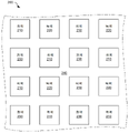
도 2는 단일 기판(240)에 의해 지지되는 다수의 마이크로LED 구조체(210, 220, 230)를 구비하는 하나의 예시적인 LED 어레이(200)의 일부분을 도시하는 평면도이며, 이 LED 어레이(200)는 디스플레이에 사용될 수 있다. 마이크로LED 구조체들(210, 220, 230)은 각각 적색, 녹색 및 청색 파장의 광을 방출할 수 있다. 비록 LED 어레이(200)의 일부분이 16개의 마이크로LED 구조체를 갖는 것으로 도시되어 있지만, LED 어레이(200)는 예를 들어 디스플레이에 사용될 수 있는 마이크로LED 구조체들(210, 220, 230)로 된 훨씬 더 큰 어레이일 수 있고, 마이크로LED 구조체들(210, 220, 230)은 픽셀들(예컨대, 마이크로LED 구조체들(210, 220, 230)의 그룹 또는 서브 어레이)로 배열될 수 있다. 이러한 경우, 특정 애플리케이션용으로 LED 어레이(200)를 맞춤화하기 위해 제조 도중에 픽셀들의 배열 형태, 그 형상, 개수, 크기 및 상응하는 파장 방출을 구성할 수 있다. 특정 실시예에서, LED 어레이(200)는 라이트필드 애플리케이션에 사용되는 것과 같은 고해상도, 고밀도 디스플레이에 사용된다. 다른 실시예에서, LED 어레이(200)는 증강 현실(AR) 또는 가상 현실(VR) 애플리케이션을 위한 컴팩트 디스플레이에 포함될 수 있다.2 is a plan view illustrating a portion of one
특히, 고밀도의 이미터를 얻기 위해, 서로 호환될 수 있는 프로세스들을 이용하여 단일구조로 통합되게 마이크로LED 구조체들(210, 220, 230)을 기판(240) 위에 형성하는 것이 바람직하다. 즉, 별도의 기판 위에 각각의 유형의 마이크로LED 구조체를 형성하고(예컨대, 제1 기판 위의 하나 이상의 적색 발광 마이크로LED 구조체, 제2 기판 위의 하나 이상의 녹색 발광 마이크로LED 구조체 및 제2 기판 위의 하나 이상의 청색 발광 마이크로LED 구조체), 그 다음에 각각의 마이크로LED 구조체를 제4 기판으로 전사하여 디스플레이에 사용할 마이크로LED 어레이를 형성하는 대신, 3가지 유형 전부의 마이크로LED 구조체(210, 220, 230)의 어레이가 기판(240) 위에 직접 형성된다. 3가지 유형 전부의 마이크로LED 구조체(210, 220, 230)를 어레이로 기판(240)(예컨대, 단일 기판) 위에 바로 형성하는 것에 의해, 보다 고밀도의 LED 어레이가 형성될 수 있다. 달리 말하면, 각각의 색상의 마이크로LED 구조체(210, 220, 230)를 별도의 웨이퍼에 형성하고 각각의 LED를 다른 기판으로 전사하여 디스플레이용 LED 어레이를 형성하는 대신, 마이크로LED 구조체들(210, 220, 230)이 기판(240) 위에 바로 형성되기 때문에 LED 어레이(200)는 보다 고밀도를 달성한다.In particular, to obtain a high-density emitter, it is desirable to form the
그러나 풀컬러 디스플레이(예컨대, 적녹청(RGB) 디스플레이)를 생산하는 데 필요한 파장 범위에 걸쳐 효율적인 발광에 맞는 프로세스 및 재료를 이용하여 마이크로LED 구조체를 형성하는 것이 극히 어렵다는 것이 기존의 문헌에 잘 정리되어 있다. 인듐-갈륨-질화물(InGaN) QW를 기반으로 하는 것과 같은 고효율이며 대형(예컨대, 치수가 수백 미크론)인 질화물 기반의 청색 LED 및 알루미늄-갈륨-인듐-인화물(AlGaInP)을 기반으로 하는 것과 같은 고효율이며 대형인 인화물 기반 적색 LED는 쉽게 구할 수 있지만, 비슷하게 높은 효율로 작동하는 녹색 LED의 부재로부터 초래되는 "녹색갭"이 수십 년 동안 알려져 왔다. 각각의 방출 범위(예컨대, 적색, 녹색, 청색)의 각각의 유형의 LED를 형성하는 전통적인 접근 방법은 그 자체로 최적화된 프로세스를 사용하고 나서 만들어진 LED 구조체를 별도의 디스플레이 기판으로 전사하여 LED 어레이를 형성한다. 이러한 접근 방법은 독립적으로 형성된 마이크로LED 구조체를 별도의 디스플레이 기판으로 전사할 수 있게 하기 위해 요구되는 LED의 최소 크기 및 고밀도 마이크로LED 어레이를 형성하도록 마이크로LED 구조체를 정확하게 정렬하기 위해 필요한 정렬 적합성(alignment fidelity)과 관련한 제약이 있다. 본 실시예의 하나의 태양은 단일 기판 위에 마이크로LED 구조체들(예컨대, 적색, 녹색 및 청색 발광 마이크로LED 구조체들)의 어레이를 형성하여 유사한 휘도와 효율 레벨을 갖는 풀컬러 이미지를 만들어 내는 것이 매우 어렵다는 인식을 포함한다.However, it is well documented in the literature that it is extremely difficult to form microLED structures using processes and materials tailored to efficient light emission across the wavelength range required to produce full color displays (e.g., red, green and blue (RGB) displays). have. High efficiency, such as those based on indium-gallium-nitride (InGaN) QW, large (e.g. hundreds of microns in dimension) nitride-based blue LEDs and high efficiency, such as those based on aluminum-gallium-indium-phosphide (AlGaInP) Phosphide-based red LEDs are readily available, but the “green gap” resulting from the absence of green LEDs operating at similarly high efficiencies has been known for decades. The traditional approach of forming each type of LED of each emission range (e.g., red, green, blue) uses an in-house optimized process and then transfers the resulting LED structure to a separate display substrate to form an LED array. form This approach provides the minimum size of LED required to enable transfer of the independently formed microLED structure to a separate display substrate and the alignment fidelity required to accurately align the microLED structure to form a high-density microLED array. ) has some limitations. One aspect of this embodiment is the recognition that it is very difficult to form an array of microLED structures (e.g., red, green and blue light emitting microLED structures) on a single substrate to produce a full color image with similar luminance and efficiency levels. includes
본 실시예는 다수의 색상의 마이크로LED 구조체들의 단일구조 통합과 호환되는 재료 및 제조 프로세스를 사용하면서 보다 긴 파장에서 고효율 마이크로LED 구조체를 달성하도록 액티브 소자를 양자우물(QW) 내에 포함시키는 것을 제어하기 위한 마이크로LED 구조체 디자인 및 제조 프로세스를 이용하여 이 문제를 해결한다. 보다 구체적으로, 본 실시예는 보다 짧은 파장(예컨대, 청색 및 녹색)의 고효율 마이크로LED 구조체의 제조에 호환되는 재료를 이용하여 보다 긴 파장(예컨대, 적색)의 고효율 마이크로LED 구조체의 형성을 가능하게 하고 이에 따라 각기 다른 색상을 발광하는 마이크로LED 구조체들의 단일구조로 통합된 어레이의 구현을 가능하게 하는 장치 구조체 및 제조 프로세스를 개시한다. 그러나 여기서 개시하는 기술이 예를 들어 적색 전용 마이크로LED 구조체를 포함하는, 모든 크기와 구성 형태의 에피택셜하게 형성되는 LED에 적용될 수 있음을 강조하는 바이다.This embodiment provides a method for controlling the incorporation of an active device into a quantum well (QW) to achieve a high-efficiency microLED structure at longer wavelengths while using materials and fabrication processes compatible with monolithic integration of multi-color microLED structures. This problem is solved by using a microLED structure design and manufacturing process for More specifically, this embodiment enables the formation of high-efficiency microLED structures of longer wavelengths (eg, red) using materials compatible with the manufacture of high-efficiency microLED structures of shorter wavelengths (eg, blue and green). and thus a device structure and fabrication process enabling the realization of a monolithically integrated array of microLED structures that emit different colors. However, it is emphasized that the techniques disclosed herein are applicable to epitaxially formed LEDs of all sizes and configurations, including, for example, red-only microLED structures.
위에서 언급한 바와 같이, 별도로 제조되는 고효율이고 대형인 질화물 기반 청색 LED와 인화물 기반 적색 LED가 공지되어 있다. 보다 긴 파장의 LED(예컨대, 적색)을 위한 질화물 기반 QW 발광 구조체를 형성할 때, 층 균일성을 유지하고 결함을 제어하면서 보다 긴 파장 방출을 달성하기 위해 QW 내의 필요한 액티브 재료, 예컨대 인듐(In)의 백분율 조성을 증가시키는 것은 어렵다. 특히, 특별히 높은 반응물질 증기압 하에서, QW 내에서 양호한 균일성을 갖는 희망하는 높은 백분율의 In을 얻는 것은 어렵다. 인듐 백분율의 감소는 공칭적인 디자인의 LED보다 QW 구조체로부터 더 짧은 파장이 방출되는 것으로 이어진다. 또한, In 클러스터링, 상 분리 및 피팅(pitting)과 같은 결함이 QW 구조체 내에서 흔히 나타난다. 적절한 재료 품질을 유지하면서 이루어지는 In 조성의 개선이 통상의 갈륨질화물(GaN)/InGaN/GaN 재료 및 성장 기술의 한계에 도달하기 전에 성장 조건 파라미터(예컨대, 온도, 시간, 증기압)를 통해 이용 가능한 조정은 제한적이다.As mentioned above, separately manufactured high-efficiency and large-size nitride-based blue LEDs and phosphide-based red LEDs are known. When forming a nitride-based QW light emitting structure for longer wavelength LEDs (eg, red), a necessary active material in the QW, such as indium (Indium), is required to achieve longer wavelength emission while maintaining layer uniformity and controlling defects. ) is difficult to increase. In particular, it is difficult to obtain the desired high percentage of In with good uniformity within the QW, especially under high reactant vapor pressures. A reduction in the percentage of indium leads to shorter wavelengths being emitted from the QW structure than the nominally designed LED. In addition, defects such as In clustering, phase separation and pitting are common in QW structures. Tuning available through growth condition parameters (e.g., temperature, time, vapor pressure) before improvements in In composition while maintaining adequate material quality reach the limits of conventional gallium nitride (GaN)/InGaN/GaN materials and growth techniques. is limited
MQW 구조체에 액티브 InGaN QW층을 증착하기 전에 알루미늄(Al)으로 된 얇은 층을 하부층으로 포함시키면 QW 내의 정공 농도가 증가함으로 인해 청색 LED 성능의 개선이 이루어지고 알루미늄 갈륨 질화물(AlGaN)/InGaN 계면에서의 추가적인 분극 전하 전하 및 점 결함의 어느 정도의 감소 가능성에 기여하는 것으로 나타났다. 이러한 기술은 1nm AlGaN층, 3.5nm 두께의 InGaN QW층 그 다음으로 배리어층으로 5nm GaN충을 적층하는 것을 이용하여 실리콘 기판 위에 청색 LED를 생성하는 데 사용되었다("Si(111) 기판 위에서 성장한 InGaN/GaN MQW에 얇은 AlGaN 중간층을 구비하는 고효율 청색 LED", S. Kimura 외, Proc. of SPIE Vol. 9748, 97481U). 하부층으로 Al과 같은 재료를 포함하면 액티브 영역 내 캐리어 분포 및 결함 감소에 도움이 되는 것으로 보인다.Inclusion of a thin layer of aluminum (Al) as an underlayer before depositing the active InGaN QW layer on the MQW structure improves the blue LED performance due to the increase in the hole concentration in the QW and at the aluminum gallium nitride (AlGaN)/InGaN interface. It has been shown that the additional polarization of charge contributes to some degree of reduction potential of charge and point defects. This technique was used to create a blue LED on a silicon substrate using a layer of 1 nm AlGaN, a 3.5 nm thick InGaN QW layer followed by a layer of 5 nm GaN as a barrier layer ("InGaN grown on a Si(111) substrate"). /High Efficiency Blue LED with Thin AlGaN Interlayer on GaN MQW", S. Kimura et al., Proc. of SPIE Vol. 9748, 97481U). Including a material such as Al as the bottom layer appears to help reduce defects and carrier distribution in the active region.
그러나 InGaN QW 내에 Al을 포함하는 것은 청색 LED에 대해서는 가능하지만, 통념에 의하면 적색 LED에 Al을 포함하는 것은 적절하지 않을 것이다. 특히, Al은 In에 비해 밴드갭이 더 넓은 재료이기 때문에, QW 구조체 내에 Al을 포함하면 QW의 전체 밴드갭이 더 넓어질 수 있으며, 이에 따라 이미터 파장에 청색 편이(즉, 보다 짧은 파장을 향한 편이)가 일어날 수 있다. 이러한 청색 편이는 청색 LED에 대해서는 쉽게 보상할 수 있지만, 적색 LED의 일반적인 목적은 보다 긴 파장의 발광을 달성하는 것이고 이에 따라 적색 LED의 QW 구조체 내에 Al을 포함하는 것은 역효과를 낳는 것으로 보일 것이다.However, while inclusion of Al in InGaN QWs is possible for blue LEDs, conventional wisdom would not be appropriate to include Al in red LEDs. In particular, since Al is a material with a wider bandgap than In, the inclusion of Al in the QW structure can lead to a wider overall bandgap of the QW, thereby giving the emitter wavelength a blue shift (i.e., a shorter wavelength). direction) can occur. While this blue shift can easily be compensated for for blue LEDs, the general purpose of red LEDs is to achieve longer wavelength emission and thus including Al in the QW structure of a red LED would appear to be counterproductive.
이전에는, 질화물 기반 청색 LED의 방출 파장을 녹색 및 심지어 적주황색 파장까지 확장하고자 하는 시도에서 QW 구조체를 캡핑하기 위해 얇은 AlGaN층(예컨대, 1 내지 2nm 두께의 층)이 사용하는 것이 행해졌었다. 예를 들어, 1nm 두께의 AlGaN층이 3nm 두께의 InGaN QW 층 바로 위에 캡층으로 증착되고 나서, MQW 구조에서 10nm 두께의 InGaN 배리어층으로 덮혀 외부 양자 효율(EQE) 값이 11% 내지 20% 범위인 녹황색, 황색 및 호박색 파장에서의 발광을 달성한다(Hashimoto, "신규한 액티브 영역을 이용한 녹색갭 처리", www.compoundsemiconductor.net, 2014년 3월, p.44). Hashimoto의 논문은 AlGaN 캡층이 전자의 파동 함수를 우물의 내부를 향해 편이시켜, 전자-정공 중첩 및 복사 재결합을 증가시키고 그리고 InGaN 우물 뒤의 표면의 평활도를 회복시키면서 전자 오버플로우에 대한 장벽을 생성하는 역할을 하는 것으로 추측한다. 또 다른 예로, 동일한 기술, 즉 1nm 두께의 AlGaN층을 각각의 QW층(즉, 755℃에서 성장한 3nm 두께의 인듐-갈륨-질화물(InGaN) 액티브층에 후속하는 역시 동일한 온도에서 성장한 1nm AlGaN층 위에 855℃에서 성장한 10nm InGaN층을 배리어층으로 덮음)의 캡층으로 포함시키면 EQE값이 2.9%로 낮음에도 불구하고 적색 파장 범위 중의 보다 짧은 가장자리에 있는 629nm의 파장에서 작동하는 LED를 생성하는 것으로 나타났다(J.I. Hwang 외, "(0001) 극성 구조 위에서 성장한 InGaN 기반 적색 LED의 개발", Applied Physics Express 7, 071003(2014)). 그러나 AlGaN 캡층은 적색 LED의 보다 짧은 파장을 향한 발광 편이 및 낮은 EQE값의 일반적인 원인인 QW 구조체 자체 내의 In과 관련된 결함을 방지하는 것으로 보이지는 않는다. 사실, Hwang 외는 생성된 LED를 구동하는 주입 전류의 증가와 함께 방출 파장에서 적색 편이가 없는 것을 특별히 언급하고 있다. 또한, 위에서 보고된 실험 결과 전부에서, LED 장치들 각각은 각 면의 치수가 수백 미크론인 대면적 장치이다.Previously, it has been done to use thin AlGaN layers (eg, 1-2 nm thick layers) to cap QW structures in attempts to extend the emission wavelengths of nitride-based blue LEDs to green and even red-orange wavelengths. For example, a 1 nm thick AlGaN layer is deposited as a capping layer directly over a 3 nm thick InGaN QW layer, then covered with a 10 nm thick InGaN barrier layer in an MQW structure to achieve an external quantum efficiency (EQE) value in the range of 11% to 20%. Luminescence at green-yellow, yellow and amber wavelengths is achieved (Hashimoto, "Green-gap treatment using a novel active region", www.compoundsemiconductor.net, March 2014, p.44). Hashimoto's paper demonstrates that the AlGaN cap layer shifts the wave function of electrons toward the interior of the well, increasing electron-hole overlap and radiative recombination and creating a barrier to electron overflow while restoring the smoothness of the surface behind the InGaN well. assumed to play a role. In another example, using the same technique, a 1 nm thick AlGaN layer is placed on top of each QW layer (i.e. a 1 nm AlGaN layer grown at 755°C followed by a 3 nm thick indium-gallium-nitride (InGaN) active layer also grown at 755°C). Inclusion of a 10 nm InGaN layer grown at 855 °C as a capping layer (covered with a barrier layer) has been shown to produce an LED operating at a wavelength of 629 nm, which is on the shorter edge of the red wavelength range, despite a low EQE of 2.9% ( J.I. Hwang et al, "Development of InGaN-based red LEDs grown on (0001) polar structures", Applied Physics Express 7, 071003 (2014). However, the AlGaN cap layer does not appear to prevent In-related defects within the QW structure itself, which is a common cause of emission shift towards shorter wavelengths and low EQE values of red LEDs. In fact, Hwang et al. specifically note the absence of a redshift in the emission wavelength with an increase in the injection current driving the resulting LED. Further, in all of the experimental results reported above, each of the LED devices is a large-area device with dimensions on each side of hundreds of microns.
아래에서 보다 상세하게 논의하는 예상치 못한 결과로, 그러한 통념과 반대로, MQW 구조체 내에 균일하게 혹은 그 안의 하나 이상의 장소에 Al을 포함하는 것이 보다 긴 파장 방출의 고효율 생성을 포함하는 적색 LED의 성능 개선을 실제로 초래하는 것을 알았다. 특히, 액티브 양자우물 자체의 내에서도 하부층, 캡층 및 그 조합에 알루미늄을 적절하게 혼입함으로써 한 변의 치수가 1미크론정도로 작은 마이크로LED의 경우에서도 고효율과 함께 그리고 가시광선 스펙트럼의 (예컨대 635nm보다 긴) 적색 범위 내에서 예상치 못한 적색 LED의 성능 개선이 초래되었다.Contrary to conventional wisdom, with unexpected consequences discussed in more detail below, the inclusion of Al either uniformly within the MQW structure or at one or more locations therein may improve the performance of red LEDs, including high-efficiency production of longer wavelength emission. I found out what actually causes it. In particular, even in the case of a microLED with a side dimension as small as 1 micron, by appropriately incorporating aluminum into the lower layer, cap layer, and combinations thereof, even within the active quantum well itself, with high efficiency and a red range of the visible light spectrum (e.g., longer than 635 nm) An unexpected improvement in the performance of red LEDs within
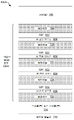
도 3은 모폴로지 및 변형 특성이 개선된 제1 및 제2 준비층(320, 330)을 구비하는 하나의 예시적인 마이크로LED 구조체(300)를 개략적으로 도시하는 단면도이다. LED 구조체(300)는 반도체 템플릿(310)(예컨대, 지지층)의 표면 위에 형성된다. LED 구조체(300)는 반도체 템플릿(310) 위에 형성되거나, 성장하거나(예컨대, 에피택셜 성장) 혹은 증착된 제1 준비층(320)(준비층 1), 제1 준비층(320) 위에 형성되거나, 성장하거나 혹은 증착된 제2 준비층(330)(준비층 2), 제2 준비 층(330) 위에 형성되거나, 성장하거나 혹은 증착된 액티브 QW 영역(340), 및 액티브 QW 영역(340) 위에 형성되거나, 성장하거나 혹은 증착된 접촉층들(예컨대, p도핑층)을 포함하는 p층들(350)을 포함한다. 일부 구현예에서, 반도체 템플릿(310) 위의 LED 구조체(300)의 위치, 형상 및 크기를 규정하기 위해 에피택셜 성장 및 건식 에칭 또는 선택적 영역 성장과 같은 기술이 사용될 수 있다. 3 is a schematic cross-sectional view of one
제1 준비층(320)과 제2 준비층(330)은 액티브 QW 영역(340)의 형성을 위해 사용되는 표면이 액티브 QW 영역(340)이 개선된 재료 특성과 발광 성능을 가지기에 적절한 모폴로지 및 변형을 가지게 준비하도록 구성된다. 이를 위해, 제1 준비층(320), 제2준비 층(330) 또는 이 둘 다가 알루미늄 함유층과 같이 밴드갭이 높은 재료를 포함한다. 예를 들어, 알루미늄 함유층은 5% 내지 100% 범위의 Al 조성을 갖는 AlInGaN 합금을 포함한다. 제1 및 제2 준비층(320, 330) 각각은 그 두께가 0.3나노미터 내지 250나노미터일 수 있다.The
액티브 QW 영역(340)은 LED 구조체(300)가 작동하는 동안 발광하도록 구성된다.
하나의 예에서, 제1 준비층(320)은 알루미늄 함유층이고 초격자(superlattice)를 포함한다. 초격자는 예를 들어 AlInGaN층과 AlGaN층이 교대로 적층되는 것에 의해 형성될 수 있다. 일 예에서, 초격자는 각기 다른 Al 및 In 조성을 갖는 AlInGaN층 및 AlGaN층이 교대로 적층되는 것에 의해 형성될 수 있다. 다른 예에서, 제1 준비층(120)은 벌크층이다. 벌크층은 알루미늄 함유층일 수 있다. 액티브 QW 영역(340)과 달리, 제1 및 제2 준비층(320, 330) 각각은 각각 액티브 QW 영역(340)과 동일한 가시광선 파장의 광을 방출하도록 구성되지 않는다. 예를 들어, 액티브 QW 영역(340)이 적색 파장의 광을 방출하도록 의도된 경우, 제1 또는 제2 준비층에 포함된 초격자는 액티브 QW 영역(340)의 의도된 기능과 간섭하지 않도록 녹색, 청색 또는 심지어 자외선 파장의 파장과 연관될 수 있다.In one example, the
일예로, 제2 준비층(330)은 위에서 언급한 바와 같이 알루미늄 함유층일 수 있다. 일 예에서, 제2 준비층(330)은 초격자, 벌크층, LED 구조체(300)의 작동 중에 액티브 QW 영역(340)과 동일한 파장의 광을 방출하도록 구성되지 않은 하나 이상의 QW 구조체를 포함할 수 있다. 또한, 제2 준비층(330)이 단일 양자우물 또는 다중 양자우물을 포함하는 경우, 제2 준비층(330)은 단일 양자우물 또는 다중 양자우물의 아래에 또는 그 위에 형성된 AlGaN층과 같은 밴드갭이 높은 중간층을 추가로 포함할 수 있다. 각각이 Al 함유층과 같이 밴드갭이 높은 재료를 혼입한 제1 및 제2 준비층들(320, 330)을 포함하면 액티브 QW 영역(340)의 발광 특성이 개선된다. 예를 들어 고온에 대한 내성 증가, 이동 불순물 가둠, 변형 특성 개선 및 액티브 QW 영역의 화학양론 최적화와 같은 그렇지만 이에 한정되지는 않는 유리한 효과를 제공하는 것에 의해, 액티브 QW의 방출 파장 사양, 방출 파장 피크 축소 및 방출 강도와 같은 발광 성능이 개선될 수 있다.For example, the second preparation layer 330 may be an aluminum-containing layer as described above. In one example, the second preparation layer 330 may include a superlattice, bulk layer, or one or more QW structures that are not configured to emit light of the same wavelength as the
도 4는 모폴로지 및 변형 특성이 개선된 하나의 예시적인 LED 구조체(400)를 개략적으로 도시하는 단면도이다. LED 구조체(400)는 도 3의 LED 구조체(300)와 유사하고, GaN 템플릿 또는 지지층일 수 있는 반도체 템플릿(310)의 표면 위에 형성된다. LED 구조체(400)는 인액티브 QW층(410), AlGaN층(420), 액티브 QW 영역(340) 및 p층(350)을 포함한다. 인액티브 QW층(410)과 AlGaN층(420)의 단일한 조합만이 도시되어 있지만, LED 구조체(400)는 인액티브 QW층(410)과 AlGaN층(420)의 다수의 또는 반복적인 조합을 포함할 수 있다. 인액티브 QW층(410)은 액티브 QW 영역(340)의 방출 파장보다 짧은 파장과 연관될 수 있다. 예를 들어, 액티브 QW 영역(340)이 적색 파장의 광을 방출하도록 구성되면, 인액티브 QW층(410)은 녹색, 청색 또는 자외선의 파장과 연관될 수 있다. AlGaN층(420)은 In 대비 5% 내지 100% 범위의 Al 조성을 갖는 AlInGaN 합금과 같이 AlGaN을 포함하는 여러 가지 합금으로 만들어질 수 있다.4 is a cross-sectional view schematically illustrating one
도 3의 LED 구조체(300)와 비교하여. LED 구조체(400)는 인액티브 QW층(410)에 적어도 하나의 QW를 포함하며, AlGaN층(420)이 적어도 하나의 QW 위에 형성된다. 예를 들어, 단일의 또는 다수의 인액티브 QW를 포함할 수 있는 인액티브 QW층(410)은 제1 준비층(320)에 상응하고, AlGaN층(420)은 제2 준비층(330)에 상응한다. 비록 도 4가 인액티브 QW층(410) 및 AlGaN층(420)의 단일 쌍만을 도시하고 있지만, LED 구조체(400)는 그 범위를 벗어나지 않으면서 인액티브 QW층(410) 및 AlGaN층(420)의 다수의 적층된 쌍을 포함할 수 있다.Compared to the
도 5는 지향성이 개선된 하나의 예시적인 LED 구조체(500)를 개략적으로 도시하는 단면도이다. LED 구조체(500)는 도 3의 LED 구조체(300)와 유사하고, 반도체 템플릿(310)의 표면 위에 형성된다. LED 구조체(500)는 제1 준비층(320), 반사층(510), 액티브 QW 영역(340) 및 p층(350)을 포함한다. 반사층(510)은 AlInN/GaN 하부 거울 또는 AlInGaN/InGaN 하부 거울일 수 있으며, 액티브 QW 영역(340)보다 먼저 형성될 수 있다. 다른 예에서, 반사층(510)은 각기 다른 Al 및 In 조성을 갖는 AlInGaN/AlInGaN을 포함할 수 있다. 따라서, 반사 층(510)은 반사 스택을 형성하는 적어도 하나의 알루미늄 함유층을 포함할 수 있다. 반사층(510)이 AlInN/GaN 하부 거울인 경우, AlInN층은 GaN에 격자 정합될 수 있는 In 대비 약 82%의 Al 함량을 가지며, 이에 따라 In 대비 대략 50%의 Al 함량을 갖는 AlGaN/GaN 시스템과 비슷한 7%의 높은 굴절율 차이를 유지하면서 후속하는 액티브층에서의 변형과 관련한 문제를 방지할 수 있다.5 is a schematic cross-sectional view of one
또한, 반사층(510)은 액티브 QW 영역(340)에 의해 생성되는 방사 패턴이 특정 애플리케이션에 맞춰질 수 있게 하고 이에 따라 액티브 QW(340)로부터의 방출의 지향성을 개선시키는 분포 브래그 반사기(DBR)일 수 있거나 혹은 그 역할을 하도록 구성될 수 있다. 예를 들어, 반사층(510)이 DBR이거나 DBR로 작동하도록 구성되면, LED 구조체(500)는 공진 공동 LED 또는 수직 공동 표면 발광 레이저(VCSEL)로 작동하도록 구성될 수 있다. 즉, p층(350)과 반사층(510)이 QW(340)를 함유하는 공진 공동을 형성하고, 이에 따라 LED 구조체(500)가 액티브 QW(340)로부터 나오는 광의 의도된 방출 파장에 대한 액티브 QW(340)의 두께에 따라 공진 공동 LED 또는 VCSEL로 작동할 수 있다.Reflective layer 510 may also be a distributed Bragg reflector (DBR) that allows the radiation pattern produced by
위에서 설명한 LED 구조체들(300, 400, 500) 각각은 에피택셜 성장 및 건식 에칭 또는 선택적 영역 성장과 같은 기술에 의해 직경 크기 또는 피처 크기가 최대 1미크론이도록 제조될 수 있고, 이는 고밀도 애플리케이션에 적합하다. 특정 실시예에서, 직경 크기는 1미크론보다 크고, 예를 들어 1미크론 내지 10미크론이다.Each of the
알루미늄 함유층을 사용하면 소형 LED의 제조 및 이러한 소형 LED의 단일구조 통합과 관련하여 LED 구조체(300, 400, 500)에 의해 제공되는 모폴로지, 변형 및 지향성 이점 외에 다른 이점이 있다. 이러한 알루미늄 함유층은 불순물을 포획하는 게터(getter)로 작용할 수 있고, 이에 의해 LED 구조체의 패시브 영역에 불순물들을 국부화시킴으로써 액티브 영역(예컨대, 액티브 QW 영역(340))의 불순물을 감소시킬 수 있다. 또한, 포획되거나 국부화된 불순물은 후속 공정 작업에서 고온이 가해지는 경우에도 이동이 방지될 수 있다. 도 4의 예에서. 인액티브 QW층(410) 위에 성장한 AlGaN층(420)은 불순물(예컨대, 산소)을 게터링하여 불순물(예컨대, 산소)이 액티브 QW 영역(340)에 혼입되는 것을 감소시키는 데 사용될 수 있다. 도 5의 예에서, 반사층(510)을 형성하기 위해 사용되는 AlInN층 또한 산소 게터링층의 역할을 할 수 있다.The use of an aluminum-containing layer provides other advantages in addition to the morphological, strain and directivity advantages provided by
도 6은 정공 누설을 감소시키는 것에 의해 성능이 개선된 하나의 예시적인 LED 구조체(600)를 개략적으로 도시하는 단면도이다. LED 구조체(600)는 도 3의 LED 구조체(300)와 유사하며, 반도체 템플릿(310)의 표면 위에 형성된다. LED 구조체(600)는 제1 준비층(320), 정공 차단층(610), 액티브 QW 영역(340) 및 p층(350)을 포함한다. 정공 차단층(610)은 반도체 템플릿(310) 및 제1 준비층(320)으로부터 액티브 QW 영역(340)으로의 정공 오버플로우 및 액티브 QW 영역(34)으로부터 제1 준비층(320) 및 반도체 템플릿(310)으로의 정공 오버플로우를 방지한다. 특정 실시예에서, 정공 차단층(610)은 n-AlGaN을 포함할 수 있다. 다른 실시예에서, 정공 차단층(610)은 액티브 QW 영역(340)의 방출 효율을 개선하는 AlGaN/GaN층 또는 InAlN/GaN층으로 형성된 초격자이다. 그러나 정공 차단층(610)은 n-AlGaN, n-도핑된 AlGaN/GaN 초격자 및 n-도핑된 InAlN/GaN 초격자를 포함하는 다른 적당한 재료를 사용할 수 있다. 6 is a schematic cross-sectional view of one
도 7은 액티브 MQW 영역(730) 내에 알루미늄이 도입된 하나의 예시적인 마이크로LED 구조체(700)를 개략적으로 도시하는 단면도이다. 마이크로LED 구조체(700)는 하나 이상의 벌크층 또는 준비층(720), 액티브 MQW 영역(730) 및 적어도 하나의 p층(740)을 지지하기 위한, 반도체 기판이라고도 알려진, 반도체 템플릿(710)을 포함한다. 액티브 MQW 영역(730)은 벌크층 또는 준비층(720) 위에 형성될 수 있고, 알루미늄을 포함하는 적어도 하나의 액티브 QW 스택(732)을 포함하는데, 액티브 QW 스택은 인접 배리어층(734)(예컨대, GaN 또는 InGaN 배리어층)을 구비한다. 각각의 액티브 QW 스택(732)은 알루미늄 함유 재료로 된 단일 층을 포함할 수 있거나, 혹은 각기 다른 재료로 된 2 이상의 층을 포함하되 이 층들 중 적어도 하나의 층이 알루미늄을 함유할 수 있다. 도 7의 예는 각각이 인접 배리어층(734)을 갖는 4개의 액티브 QW 스택(732)을 구비하는 액티브 MQW 영역(730)을 도시하고 있지만, 마이크로LED 구조체(700)의 희망하는 발광 성능에 따라 더 적거나 혹은 더 많은 수의 액티브 QW 스택(732) 및 상응하는 배리어층(734)이 포함될 수 있다.FIG. 7 is a schematic cross-sectional view of one
위에서 언급한 바와 같이, In에 비해 밴드갭이 더 넓은 재료인 Al을 포함하면 만들어지는 마이크로LED 구조체로부터 보다 짧은 파장의 발광이 이루어질 것으로 보일 것이다. 그러나 그러한 직관과는 반대로, Al을 적절하게 포함하면 Al을 포함하지 않는 마이크로LED 구조체와 비교하여 효율과 광발광 성능이 더 높은 마이크로LED 구조체가 만들어진다. 구체적으로, Al을 포함하면 위에서 논의한 바와 같이 LED 구조체 전체에 걸쳐 전류 밀도가 증가하면서 마이크로LED 구조체로부터 방출되는 파장이 보다 짧은 파장을 향해 편이되고(예컨대, 청색 편이), 이에 따라 청색 편이를 보상하기 위해 전체 마이크로LED 구조체의 조정이 필요하다. 액티브 QW 영역의 그리고 그 주변의 특정 층과 같이 액티브 QW 스택(732) 내에 Al을 혼입하는 여러 가지 방법을 개시하는데, 이에 대해서는 아래에서 보다 상세하게 설명한다.As mentioned above, the inclusion of Al, which is a material with a wider bandgap than In, would seem to result in shorter wavelength light emission from the resulting microLED structure. Contrary to that intuition, however, appropriate inclusion of Al results in microLED structures with higher efficiency and photoluminescent performance compared to microLED structures that do not contain Al. Specifically, the inclusion of Al shifts the wavelength emitted from the microLED structure toward a shorter wavelength (e.g., blue-shift) while increasing the current density across the LED structure as discussed above, thereby compensating for the blue-shift. For this, it is necessary to adjust the entire microLED structure. Several methods of incorporating Al into the active QW stack 732, such as specific layers in and around the active QW region, are described in more detail below.
도 8a 및 도 8b는 액티브 MQW 영역(830A, 830B) 내에 알루미늄을 함유하는 하부층을 각각 포함하는 예시적인 마이크로LED 구조체들(800A, 800B)을 개략적으로 도시하는 단면도들이다. 마이크로LED 구조체들(800A, 800B)은 도 7의 마이크로LED 구조체(700)와 유사하다. 액티브 MQW 영역(830A, 830B)은 벌크층 또는 준비층(720) 위에 형성된다. 도 8a는 4개의 액티브 QW층(832)으로 된, 집합적으로 QW 스택이라고 하는, 스택을 포함하는 마이크로LED 구조체(800A)의 액티브 MQW 영역(830A)을 도시한다. 각각의 QW층(832)은 배리어층(734)에 의해 분리되는 층들의 쌍들을 형성하도록 각각의 AlGa(In)N 하부층(836)(이하, Al 하부층(836))의 상부에 증착된다. Al 하부층(836)은 그 두께 범위가 수 원자층 내지 수 나노미터일 수 있다. 이러한 두께를 넘어서면, Al 하부층(836)이 마이크로LED 구조체에 밴드갭 증가로 인한 바람직하지 않은 청색 편이를 초래할 수 있다. 액티브 QW층(832)은 InGaN으로 형성될 수 있다. Al 하부층(836)은 AlGaN, AlInN 및 InAlGaN 중 하나와 같은 알루미늄을 포함하는 합금이며, 다시 말해 마이크로LED 구조체(800A)와 같은 질화물 기반 마이크로LED 구조체의 제조 공정과 호환된다. Al 하부층(836)은 중간층이라고 말할 수 있다.8A and 8B are cross-sectional views schematically illustrating
QW 기반 LED 구조체의 액티브 QW층 아래에 AlGaN 하부층을 포함하는 것은 청색 파장에서 실시된 바 있으며, 이는 Al의 도입에 의해 초래되는 방출 파장의 청색 편이가 청색 LED와 호환된다는 점에서 개념적으로 타당하다. 그러나 Al 하부층(836)의 추가로 포함하는 것이 액티브 MQW 영역(830A)의 유효 밴드갭을 더 넓히는 것처럼 보일 것이지만, Al 하부층(836) 내에 Al을 포함하는 것은 액티브 QW층(832) 내에서 고함량의 In을 함유하는 재료의 품질 및 균일도를 개선하는 결과를 가져온다. AlGaN 또는 AlInN 하부층을 포함하면 액티브 QW층이 성장하는 결정 표면 모폴로지를 수정하여 결함을 줄이고 배리어층(734)의 성장 도중과 같은 고온 처리 도중의 재료 안정성을 개선하는 것으로 보인다. 따라서 액티브 MQW 영역(830A)의 충분히 넓은 밴드갭으로부터 발생되는 어떠한 청색 편이도 개선된 성장 모드 및 액티브 QW층(832) 내에서의 결함 감소에 의해 극복되는 것으로 보인다. 결과적으로, 마이크로LED 구조체(800A)는 도 8A에 도시된 피처들의 조합을 구비하지 않는 마이크로LED 구조체와 비교하여 예기치 않게 훨씬 우수한 효율과 보다 긴 파장 방출을 나타낸다. 예를 들어, 마이크로LED 구조체(800A)는, 그 외에는 유사한 재료 구조를 갖는 종래 기술의 LED 구조체(100)와 비교하여, 인가된 전류 밀도의 증가와 함께 파장에서 10nm 이하의 청색 편이를 갖는 유사한 피크 IQE값을 나타내는 것으로 판명되었다.Including an AlGaN sublayer under the active QW layer of a QW-based LED structure has been practiced at blue wavelengths, which makes conceptual sense in that the blue shift in emission wavelength caused by the introduction of Al is compatible with blue LEDs. However, while the additional inclusion of an Al sublayer 836 would appear to widen the effective band gap of the active MQW region 830A, the inclusion of Al in the Al sublayer 836 results in a high content in the
도 8b는 도 8a의 마이크로LED 구조체(800A)와 유사하지만 액티브 MQW 영역(830B)의 Al 하부층(836)과 액티브 QW층(832) 사이에 중간층(838)을 포함하는 마이크로LED 구조체(800B)를 도시한다. 증간층(838)은 GaN과 같은 전통적인 배리어층 재료 또는 질화물 기반 마이크로LED 제조와 호환되는 여러 가지 조성의 AlGaN, InGaN 및 AlInGaN 재료와 같은 기타 재료로 형성될 수 있다. Al 하부층(836)과 중간층(838)의 조합은 액티브 QW층(832)의 접착성과 균일성을 더 개선하고, 액티브 QW층(832)의 계면에서의 그리고 액티브 QW층 내의 결함을 감소시키고, 그리고 각각의 액티브 QW층(832) 내의 In 보유를 증가시킨다. 결과적으로, 마이크로LED 구조체(800B)의 발광은 적색 파장을 향해 편이되고, 마이크로LED 구조체(800B)의 양자 효율 성능은 Al 하부층(836)을 포함하지 않는 마이크로LED 구조체와 비교하여 개선된다. FIG. 8B shows a
도 9는 도 7의 마이크로LED 구조체(700)와 유사하고, 벌크층 또는 준비층(720) 위에 형성되는 액티브 MQW 영역(930) 내의 액티브 QW층(832) 위에 위치되는 알루미늄을 함유하는 캡층(932)(이하 Al 캡층(932)이라 함)을 더 포함하는 하나의 예시적인 마이크로LED 구조체(900)를 개략적으로 도시하는 단면도이다. 예를 들어, 두께가 대략 1나노미터 이하인 AlGaN 층이 캡층(932)으로 사용될 수 있다. Al 캡층(932)은 다른 중간층으로 지칭될 수 있다. Al 캡층(932)의 포함하는 것이 보기에는 액티브 MQW 영역(930)의 유효 밴드갭을 더 넓게 하는 결과를 초래하지만, Al 캡층(932)은 다수의 이점을 제공하는데, Al 캡층(932)은, Al 캡층(932)이 마이크로LED 구조체(800A, 800B)의 Al 하부층(836)과 같이 액티브 QW층(832)과 배리어층(734) 간의 변형의 균형을 맞추는 역할을 함으로써 액티브 QW층(832)의 성장 전후의 모폴로지를 맞출 수 있게 하고, 액티브 QW층(832) 내에 In을 유지하고, 그리고/또는 청색 편이를 최소화하면서 장파장 방출에 도움이 되는 대역 정렬을 제공하는 것과 같은 많은 이점을 제공한다. 따라서 액티브 QW층(832)은 보다 나은 In 유지성 및 균일성을 나타냄으로써, 도 9에 도시된 피처들의 조합이 없는 마이크로LED와 비교하여 효율을 훨씬 우수하게 하고 보다 긴 파장을 방출하게 한다. FIG. 9 shows a
Al 캡층(932)은 전체 구조체에 포함될 수 있는 임의의 전자 차단층 및 p층으로부터 나오는 수소를 포함하는 점결함의 이동을 막는 장벽의 역할을 할 수 있다. 그러나 여기서 Al 캡층(932)이 액티브 QW층(832) 자체 내의 결함을 방지하는 데 항상 도움이 되지 않을 수 있고 따라서 도 8a 및 도 8b에 도시된 바와 같은 Al 하부층(836)을 포함하는 것과 같은 추가적인 조치가 잠재적으로 필요하다는 것이 알려졌다.The
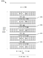
도 10은 벌크층 또는 예비층(720) 위에 형성된 액티브 MQW 영역(1030)의 적어도 하나의 액티브 QW층(1032) 내에 알루미늄을 포함하는 하나의 예시적인 마이크로LED 구조체(1000)를 개략적으로 도시하는 단면도이다. 집합적으로 QW 스택이라고 하는, 4개의 액티브 QW층(832)을 갖는 것으로 도시되어 있지만, 액티브 MQW 영역(1030)은 그 범위를 벗어나지 않으면서 더 많거나 혹은 더 적은 수의 액티브 QW층(1032)을 포함할 수 있다. 특정 실시예에서, 액티브 QW층(1032)을 증착하는 동안, Al을 액티브 QW층(1032)의 합금 조성에 예를 들어 0.01 내지 5%의 농도로 혼입시키기 위해 Al 함유 가스가 특정 농도로 도입된다. 특정 실시예에서, 이 프로세스는 Al을 포함하도록 액티브 MQW 영역(1030) 내의 모든 액티브 QW층(1032)에 대해 수행된다. 다른 실시예에서, 유사한 프로세스가 액티브 MQW 영역(1030)의 각각의 액티브 QW층(1032)에 포함된 Al의 양을 변화시키기 위해 사용된다. 예를 들어, 특정 QW층 내의 Al 포함은 유사 합금, 디지털 합금 또는 단주기 초격자의 형태일 수 있다. 액티브 MQW 영역(1030) 내에서, 액티브 QW층(1032)은 GaN과 같은 적절한 재료로 형성된 배리어층(734)에 의해 분리된다.FIG. 10 is a cross-sectional schematic illustration of one
액티브 QW층(1032) 내에 Al을 포함하는 것은 In 분포 균일성을 개선하고, 보통 액티브 QW층(1032)의 증착 도중에 요구되는 것보다 높은 대략 100℃의 온도를 요구하는, 배리어층(734)의 성장과 같은, 후속하는 고온 처리 중에 액티브 QW층(1032)으로부터 In이 탈리되는 것을 방지한다. Al의 포함하면 QW 변형을 보상함으로써 분극 유도 전기장을 수정하는 것으로 보인다. 달리 말하면, 액티브 QW층(1032)을 증착하는 동안 Al을 포함하는 것은 In 함유성 및 In 유지성을 개선하고, In 함량이 높은 InGaN 재료와 관련된 결함을 감소시키고 그리고/또는 액티브 QW층(1032) 내의 InGaN 안정성을 향상시킴으로써, Al과 같은 밴드갭이 보다 넓은 물질을 포함하는 것의 잠재적인 부작용을 극복하는 것으로 보인다. 또한, Al은 적외선, 가시광선 및 자외선 파장에서 작동하도록 구성된 (치수가 대략 수백 미크론 이상인) 전통적인 LED 및 마이크로LED 구조체 둘 다를 포함하는 발광 구조체의 다양한 파장들을 위해 액티브 MQW 영역(1030) 내의 도펀트(dopant)로 사용될 수 있다. Al은 금속 유기화학 기상 증착(MOCVD) 시스템과 같이 QW 구조체를 생성하는 데 일반적으로 사용되는 시스템에서 쉽게 이용할 수 있는 표준 전구체이기 때문에 유리하다.Including Al in the active QW layer 1032 improves the In distribution uniformity and of the
Al의 액티브 QW층(1032)에의 혼입은 액티브 QW 재료의 성장 조건(예컨대, 온도, 압력, 시간)에 따라 달라지고, 따라서 액티브 QW층(1032)에 포함되는 Al의 양은 액티브 QW층(1032)의 희망하는 성질을 제공하도록 조정될 수 있다. 액티브 MQW 영역(1030)이 4개의 액티브 QW층(1032)을 갖는 것으로 도시되어 있지만, 마이크로LED 구조체(1000)의 희망하는 발광 특성 및 작동 특성을 얻기 위해 더 많거나 혹은 더 적은 수의 액티브 QW층(1032) 및 이에 상응하는 수의 배리어층(734)이 포함될 수 있다. The incorporation of Al into the active QW layer 1032 depends on the growth conditions (e.g., temperature, pressure, time) of the active QW material, and therefore the amount of Al included in the active QW layer 1032 can be tuned to provide the desired properties of While the
도 11은 도 10의 마이크로LED 구조체(1000)와 유사하고 도 8a 및 도 8b의 마이크로LED 구조체(800A, 800B)의 하부층(836)과 같이 알루미늄을 함유하는 하부층을 더 포함하는 하나의 예시적인 마이크로LED 구조체(1100)를 개략적으로 도시하는 단면도이다. 액티브 MQW 영역(1130)은 벌크층 또는 준비층(720) 위에 형성되고, Al 하부층(836) 및 액티브 QW층(1032)의 조합을 포함하는데 둘 다 Al을 포함한다. Al 하부층(836)은 액티브 QW층(1032)의 증착 균일성 및 접착성을 촉진함으로써 도 11의 피처들을 포함하지 않는 마이크로LED 구조체의 적색 파장에서의 양자 효율과 비교하여 적색 파장에서의 양자 효율을 개선하는 것으로 보인다. 특정 실시예에서, (도 8b에 도시된 바와 같은) 중간층(838)이 Al 하부층(836)과 액티브 QW층(1032) 사이에 포함될 수 있다.FIG. 11 is an
도 12는 도 10의 마이크로LED 구조체(1000)와 유사하고 도 9의 마이크로LED 구조체(900)의 Al 캡층(932)을 더 포함하는 하나의 예시적인 마이크로LED 구조체(1200)를 개략적으로 도시하는 단면도이다. 마이크로LED 구조체(1200)의 액티브 MQW 영역(1230)은 벌크층 또는 준비층(720) 위에 형성되고, 역시 Al을 포함하는 액티브 QW층(1032)을 갖는 Al 캡층(932)을 포함한다. 액티브 능동 QW층(1032)을 Al 캡층(932)으로 덮은 조합은 액티브 QW층(1032) 내의 In 유지를 촉진함으로써 액티브 MQW 영역(1230)이 없는 마이크로LED 구조체의 적색 파장에서의 양자 효율과 비교하여 적색 파장에서의 양자 효율 개선을 유도한다.FIG. 12 is a cross-sectional schematic illustration of one
도 13은 도 12의 마이크로LED 구조체(1200)와 유사하고 도 8b의 Al 하부층(836)을 더 포함하는 하나의 예시적인 마이크로LED 구조체(1300)를 개략적으로 도시하는 단면도이다. 마이크로LED 구조체(1300)는 벌크층 또는 준비층(720) 위에 형성된 액티브 MQW 영역(1330)을 구비하며, 액티브 MQW 영역은 각각의 QW층(1032)에 대해 Al 하부층(836) 및 Al 캡층(932)을 포함하고 Al 하부층(836) 및 Al 캡층(932)에 인접한 배리어층(734)을 더 포함한다. 선택적으로, 도 13에 도시된 바와 같이. Al 하부층(836)이 예를 들어 AlGa(In)N인 경우, 중간층(838)이 Al 하부층(836)과 액티브 QW층(1032) 사이에 배치될 수 있다. 액티브 MQW 영역(1330) 내에 Al을 포함하면 각각의 액티브 QW층(1032) 내의 In 분포 균일성을 개선하고, 액티브 MQW 영역(1330) 내의 In 보유를 촉진하고, 배리어층(734)이 성장하는 동안 액티브 QW층(1032)으로부터 In이 탈리되는 것을 감소시킨다. 따라서 마이크로LED 구조체(1300)는 도 8b, 도 9 및 도 10에 도시된 마이크로LED 구조체들의 유익한 효과를 결합한다.FIG. 13 is a cross-sectional view schematically illustrating one
도 14는 마이크로LED 구조체를 제조하기 위한 하나의 예시적인 프로세스(1400)를 도시하는 흐름도이다. 프로세스(1400)는 예를 들어 MOCVD 시스템 또는 마이크로LED 제조에 적합한 다른 시스템 내에서 이루어질 수 있다. 프로세스(1400)의 블록(1410)에서, 하나 이상의 벌크층 또는 준비층이 기판 위에 증착된다. 블록(1410)의 일 예에서, 제1 및 제2 준비층(320, 330)이 반도체 템플릿(310) 위에 증착된다. 블록(1410)의 다른 예에서, 벌크층 또는 준비층(720)이 반도체 템플릿(710) 위에 증착된다. 블록(1412)은 선택적인 단계이다. 포함되는 경우, 블록(1412)에서, 프로세스(1400)는 하나 이상의 배리어 재료를 증착한다. 블록(1412)의 일 예에서, 배리어층(734)은 벌크층 또는 예비층(720) 위에 증착된다. 특정 실시예에서, 블록(1412)에서 배리어 재료를 별도로 증착하는 대신 제1 배리어 재료가 블록(1410)에서 증착된 하나 이상의 벌크층 또는 준비층(720)에 혼입될 수 있음에 유의하자. 14 is a flow diagram illustrating one
블록(1420)은 결정 단계이다. 블록(1420)에서 Al을 갖는 하부층을 추가하는 것으로 결정되면, 프로세스(1400)는 블록(1422)으로 이어지고, 그렇지 않으면 프로세스(1400)는 블록(1424)으로 이어진다. 블록(1422)에서, 프로세스(1400)는 Al을 함유하는 하부층을 증착한다. 블록(1422)의 일 예에서, Al 하부층(836)은 이전에 증착된 층 위에 증착된다.
블록(1424)은 결정 단계이다. 블록(1424)에서 중간층을 추가하는 것으로 결정되면, 프로세스(1400)는 블록(1426)으로 이어지고, 그렇지 않으면 프로세스(1400)는 블록(1430)으로 이어진다. 블록(1426)에서, 프로세스(1400)는 이전에 증착된 층 위에 중간층을 증착한다. 블록(1426)의 일 예에서, 중간층(838)은 Al 하부층(836) 위에 증착된다.
블록(1430)은 결정 단계이다. 블록(1430)에서 액티브 QW층에 Al을 포함하기로 결정되면, 프로세스(1400)는 블록(1432)으로 이어지고, 그렇지 않으면 프로세스(1400)는 블록(1440)으로 이어진다. 블록(1432)에서, 프로세스(1400)는 Al을 혼입한 액티브 QW 재료를 증착한다. 블록(1432)의 일 예에서, 액티브 QW층(1032)이 배리어층(734) 위에 증착될 때 Al이 추가된다. 블록(1432)의 다른 예에서, 액티브 QW층(1032)이 Al 하부층(836) 위에 증착될 때 Al이 추가된다. 블록(1432)의 다른 예에서, 액티브 QW층(1032)이 중간층(838) 위에 증착될 때 Al이 추가된다. 그런 다음, 프로세스(1400)는 블록(1450)으로 이어진다. 블록(1440)에서, 프로세스(1400)는 Al을 추가하지 않고 액티브 QW 재료를 증착한다. 블록(1440)의 일 예에서, 액티브 QW 영역(340)이 제2 준비층(330) 위에 증착된다. 블록(1440)의 다른 예에서, 액티브 QW 층(832)이 Al 하부층(836) 위에 증착된다. 블록(1440)의 다른 예에서, 액티브 QW층(832)이 중간층(838) 위에 증착된다. 블록(1440)의 다른 예에서, 액티브 QW층(832)이 배리어층(734) 위에 증착된다.
블록(1450)은 결정 단계이다. 블록(1450)에서 Al 캡층을 포함하는 것으로 결정되면, 프로세스(1400)는 블록(1452)으로 이어지고, 그렇지 않으면 프로세스(1400)는 블록(1470)으로 이어진다. 블록(1452)에서, 프로세스(1400)는 Al 캡층을 증착한다. 블록(1452)의 일 예에서, Al 캡층(932)이 액티브 QW층(832) 위에 증착된다. 블록(1542)의 다른 예에서, Al 캡층(932)이 액티브 QW층(1032) 위에 증착된다.
블록(1470)은 결정 단계이다. 블록(1470)에서 추가 QW층이 증착되어야 하는 것으로 결정되면, 프로세스(1400)는 블록(1412)으로 이어지고, 그렇지 않으면, 프로세스(1400)는 블록(1480)으로 이어진다. 따라서 블록들(1412 내지 1470)은 추가될 각각의 추가 QW층에 대해 반복된다.Block 1470 is a decision step. If it is determined at block 1470 that an additional QW layer is to be deposited, then
블록(1480)에서, 프로세스(1400)는 배리어 재료를 증착한다. 블록(1480)의 일 예에서, 배리어층(734)은 액티브 QW 스택(732) 위에 증착된다. 블록(1480)의 다른 예에서, 배리어층(734)은 액티브 QW층(832) 위에 증착된다. 블록(1480)의 다른 예에서, 배리어층(734)은 Al 캡층(932) 위에 증착된다. 블록(1482)에서, 프로세스(1400)는 하나 이상의 p층을 증착한다. 블록(1482)의 일 예에서, 하나 이상의 p층(350)이 액티브 QW 영역(340) 위에 증착된다. 블록(1482)의 다른 예에서, p층(740)은 배리어층(734) 위에 증착된다. 그런 다음, 프로세스(1400)가 종료될 수 있다.At
본 개시는 마이크로LED 구조체로부터 방출되는 적색 파장에서의 성능을 개선하는 기술 및 구조를 사용하는 여러 가지 실시예를 설명한다. 적색 파장에서 발광하는 마이크로LED 구조체에 논의의 초점이 맞추어져 있지만, 설명한 실시예의 기술과 구조는 보다 짧은 가시광선 파장 및 적외선 파장과 같은 다른 파장 범위에서 작동하는 LED의 성능을 조정하는 데에도 또한 사용될 수 있다. 또한, 개시된 실시예가 기본적으로 질화물 기반 마이크로LED 구조체를 예시하고 있지만, 밴드갭 및 결함 처리를 위한 유사한 재료 및 적층 구조 수정이 인화물 기반 LED 구조체와 같은 다른 발광 구조체에 대해 적용될 수 있다. 또한, 개시된 실시예가 QW 구조체를 생성하는 데 일반적으로 사용되는 MOCVD 시스템에서 쉽게 이용 가능한 표준 전구체인 Al을 포함하는 것에 관한 것이지만, 마이크로LED 구조체의 MQW 영역 내에, 마이크로LED 구조체로부터의 희망하는 발광을 추가로 처리하기 위해 다른 재료를 포함하는 것을 고려할 수 있다. 더욱이, 추가 중간층이 예컨대 도 9의 액티브 QW층(832)과 Al 캡층(932) 사이에 그리고/또는 도 12 및 도 13의 액티브 QW층(1032)과 Al 캡층(932) 사이에 포함될 수 있다.This disclosure describes several embodiments that use techniques and structures to improve performance at red wavelengths emitted from microLED structures. Although the focus of the discussion is on microLED structures that emit at red wavelengths, the techniques and structures of the described embodiments can also be used to tune the performance of LEDs operating in other wavelength ranges, such as shorter visible wavelengths and infrared wavelengths. can Further, while the disclosed embodiments primarily illustrate nitride-based microLED structures, similar material and stack structure modifications for bandgap and defect handling can be applied to other light emitting structures, such as phosphide-based LED structures. Further, while the disclosed embodiments are directed to including Al, which is a standard readily available precursor in MOCVD systems commonly used to create QW structures, within the MQW region of the microLED structure, the desired emission from the microLED structure is added. You may consider including other materials for processing. Moreover, additional interlayers may be included, for example, between
LED 구조체는 적어도 하나의 양자우물을 갖는 액티브 영역을 포함할 수 있고, 액티브 영역은 LED 구조체와 연관된 발광을 제공하도록 구성된다. 일정량의 알루미늄이 적어도 하나의 양자우물 내에 혼입된다. LED 구조체의 액티브 영역은 적어도 하나의 양자우물 내에 혼입된 알루미늄의 양보다 많은 양의 알루미늄을 혼입한 적어도 하나의 알루미늄 함유층을 더 포함할 수 있다. 하나 이상의 양자우물 내에 혼입된 알루미늄의 양은 하나 이상의 양자우물의 0.01 내지 5%이다. LED 구조체는 수정된 내부 양자 효율 값을 나타내는데, 이는 적어도 하나의 양자우물 내에 혼입된 알루미늄의 양이 없는 수정되지 않은 LED 구조체에 의해 나타나는 수정되지 않은 내부 양자 효율 값보다 높다. LED 구조체는 수정된 피크 파장에서 작동하는데, 이는 적어도 하나의 양자우물 내에 혼입된 알루미늄의 양이 없는 수정되지 않은 LED 구조체의 수정되지 않은 피크 파장보다 길다. LED 구조체의 직경은 10미크론 미만이다.The LED structure can include an active region having at least one quantum well, the active region configured to provide light emission associated with the LED structure. A certain amount of aluminum is incorporated into at least one quantum well. The active region of the LED structure may further include at least one aluminum-containing layer incorporating a greater amount of aluminum than the amount of aluminum incorporated in the at least one quantum well. The amount of aluminum incorporated into the one or more quantum wells is 0.01 to 5% of the one or more quantum wells. The LED structure exhibits a modified internal quantum efficiency value that is higher than the unmodified internal quantum efficiency value exhibited by an unmodified LED structure without the amount of aluminum incorporated in the at least one quantum well. The LED structure operates at a modified peak wavelength, which is longer than the unmodified peak wavelength of an unmodified LED structure without the amount of aluminum incorporated in the at least one quantum well. The diameter of the LED structure is less than 10 microns.
LED 구조체는 LED 구조체와 연관된 발광을 제공하도록 구성된 액티브 영역을 포함하고, 액티브 영역은 배리어층 및 액티브 QW층을 포함하고, 액티브 QW층은 실질적으로 주 액티브 QW 재료로 이루어지되, 액티브 QW층은 액티브 QW층 내에 혼입된 일정량의 부 재료를 추가로 포함하고, 부 재료는 주 액티브 QW 재료보다 더 넓은 밴드갭을 나타낸다. 액티브 영역은 액티브 양자우물층 내에 혼입된 부 재료의 양보다 더 많은 양의 부 재료를 혼입한 적어도 하나의 중간층을 더 포함할 수 있다. 적어도 하나의 중간층은 배리어층과 액티브 양자우물층 사이에 배치된다. 적어도 하나의 중간층은 하부층일 수 있다. 적어도 하나의 중간층은 캡층일 수 있다. 부 재료는 알루미늄이다. LED 구조체는 수정된 내부 양자 효율 값을 나타내는데, 이 값은 적어도 하나의 양자우물 전체에 분포된 부 재료의 양이 없는 수정되지 않은 LED 구조체에 의해 나타나는 수정되지 않은 내부 양자 효율 값보다 높다. LED 구조체는 수정된 피크 파장에서 작동하는데, 이 피크 파장은 적어도 하나의 양자우물 전체에 분포된 부 재료의 양이 없는 수정되지 않은 LED 구조체가 작동하는 수정되지 않은 피크 파장보다 길다. LED 구조체의 직경은 10미크론 미만이다.The LED structure includes an active region configured to provide light emission associated with the LED structure, the active region including a barrier layer and an active QW layer, the active QW layer consisting substantially of a primary active QW material, the active QW layer comprising an active QW layer. It further includes a certain amount of sub-material incorporated into the QW layer, wherein the sub-material exhibits a wider bandgap than the main active QW material. The active region may further include at least one intermediate layer in which an amount of the sub material is incorporated in a larger amount than the amount of the sub material included in the active quantum well layer. At least one intermediate layer is disposed between the barrier layer and the active quantum well layer. At least one intermediate layer may be a lower layer. At least one intermediate layer may be a capping layer. The secondary material is aluminum. The LED structure exhibits a modified internal quantum efficiency value, which value is higher than the unmodified internal quantum efficiency value exhibited by an unmodified LED structure without the amount of secondary material distributed throughout the at least one quantum well. The LED structure operates at a modified peak wavelength, which peak wavelength is greater than the unmodified peak wavelength at which an unmodified LED structure without an amount of secondary material distributed throughout the at least one quantum well operates. The diameter of the LED structure is less than 10 microns.
방법은 배리어층 및 액티브 양자우물층을 포함하는 적어도 하나의 양자우물 영역을 포함하는 발광 다이오드(LED) 구조체를 형성한다. 적어도 하나의 양자우물 영역을 형성할 때, 주 액티브 양자우물 재료는 주 액티브 양자우물 재료보다 더 넓은 밴드갭을 나타내는 일정량의 부 재료와 함께 증착된다. 부 재료의 양은 주 액티브 양자우물 재료의 0.01 내지 5%이다. 주 액티브 양자우물 재료를 일정량의 부 재료와 함께 증착하는 것은 주 액티브 재료와 부 재료의 유사 합금을 형성하는 것을 포함한다.A method forms a light emitting diode (LED) structure comprising at least one quantum well region comprising a barrier layer and an active quantum well layer. When forming the at least one quantum well region, the main active quantum well material is deposited together with a certain amount of auxiliary material exhibiting a wider bandgap than the main active quantum well material. The amount of the secondary material is 0.01 to 5% of the main active quantum well material. Depositing the main active quantum well material together with an amount of the sub material includes forming a pseudo alloy of the main active material and the sub material.
피처들의 조합combination of features
아래의 실시예들 및 서로 호환 가능한 이러한 실시예들의 임의의 조합도 생각할 수 있다.The embodiments below and any combination of these embodiments compatible with each other are contemplated.
(A) 발광 다이오드(LED) 구조체는 반도체 템플릿 위에 형성된 벌크층 또는 준비층, 벌크층 또는 준비층 위에 형성된 액티브 영역 및 액티브 영역 위에 형성된 적어도 하나의 p층을 포함한다. 액티브 영역은 벌크층 또는 준비층 위에 형성된 제1 배리어층, 제1 배리어층 위에 형성된 적어도 하나의 알루미늄 함유 액티브 양자우물(QW) 스택, 및 액티브 QW 스택 위에 형성된 제2 배리어층을 포함한다. 적어도 하나의 액티브 QW 스택이 주입 전류에 의해 구동될 때 액티브 영역은 LED 구조체로부터 광을 방출한다.(A) A light emitting diode (LED) structure includes a bulk layer or preparation layer formed on a semiconductor template, an active region formed on the bulk layer or preparation layer, and at least one p-layer formed on the active region. The active region includes a first barrier layer formed over the bulk layer or preparation layer, at least one aluminum-containing active quantum well (QW) stack formed over the first barrier layer, and a second barrier layer formed over the active QW stack. The active region emits light from the LED structure when at least one active QW stack is driven by the injection current.
(B) (A)에서 설명한 LED 구조체에 있어서, 액티브 영역이 LED 구조체로부터 적색 파장의 광을 방출하도록 구성된다.(B) In the LED structure described in (A), the active region is configured to emit light of a red wavelength from the LED structure.
(C) (A) 또는 (B)에서 설명한 LED 구조체에 있어서, 적어도 하나의 액티브 QW 스택이 (a) 제1 배리어층 위에 형성된 알루미늄 함유 하부층 및 (b) 알루미늄 함유 하부층 위에 형성된 액티브 QW층을 포함한다.(C) The LED structure described in (A) or (B), wherein at least one active QW stack includes (a) an aluminum-containing lower layer formed on the first barrier layer and (b) an active QW layer formed on the aluminum-containing lower layer. do.
(D) (A) 내지 (C) 중 어느 하나에서 설명한 LED 구조체에 있어서, 알루미늄 함유 하부층이 AlGa(In)N, AlGaN, AlInN 및 InAlGaN으로 이루어진 군으로부터 선택된 합금을 포함한다.(D) The LED structure described in any one of (A) to (C), wherein the aluminum-containing underlayer comprises an alloy selected from the group consisting of AlGa(In)N, AlGaN, AlInN, and InAlGaN.
(E) (A) 내지 (D) 중 어느 하나에서 설명한 LED 구조체에 있어서, 적어도 하나의 액티브 QW 스택이 (c) 액티브 QW층 위에 형성된 알루미늄 함유 캡층을 더 포함한다.(E) The LED structure described in any one of (A) to (D), wherein the at least one active QW stack further includes (c) an aluminum-containing cap layer formed over the active QW layer.
(F) (A) 내지 (E) 중 어느 하나에서 설명한 LED 구조체에 있어서, 알루미늄 함유 캡층 1nm 두께의 AlGaN 재료를 포함한다.(F) In the LED structure described in any one of (A) to (E), the aluminum-containing cap layer includes an AlGaN material with a thickness of 1 nm.
(G) (A) 내지 (F) 중 어느 하나에서 설명한 LED 구조체에 있어서, 적어도 하나의 액티브 QW 스택이 (a) 제1 배리어층 위에 형성된 알루미늄 함유 하부층, (b) 알루미늄 함유 하부층 위에 형성된 중간층 및 (c) 중간층 위에 형성된 액티브 QW층을 포함한다.(G) The LED structure described in any one of (A) to (F), wherein at least one active QW stack comprises (a) an aluminum-containing lower layer formed on the first barrier layer, (b) an aluminum-containing lower layer formed on the aluminum-containing lower layer, and (c) an active QW layer formed on the intermediate layer.
(H) (A) 내지 (G) 중 어느 하나에서 설명한 LED 구조체에 있어서, 중간층이 GaN, AlGaN, InGaN 및 AlInGaN으로 이루어진 군으로부터 선택된 재료를 포함한다. (H) In the LED structure described in any one of (A) to (G), the intermediate layer includes a material selected from the group consisting of GaN, AlGaN, InGaN, and AlInGaN.
(I) (A) 내지 (H) 중 어느 하나에서 설명한 LED 구조체에 있어서, 적어도 하나의 액티브 QW 스택이 제1 배리어층 위에 형성된 알루미늄 함유 QW층을 포함한다.(I) In the LED structure described in any one of (A) to (H), at least one active QW stack includes an aluminum-containing QW layer formed over the first barrier layer.
(J) (A) 내지 (I) 중 어느 하나에서 설명한 LED 구조체에 있어서, 알루미늄 함유 QW층이 유사 합금, 디지털 합금 및 단주기 초격자 중 하나를 포함한다.(J) In the LED structure described in any one of (A) to (I), the aluminum-containing QW layer includes one of a pseudo alloy, a digital alloy and a short period superlattice.
(K) (A) 내지 (J) 중 어느 하나에서 설명한 LED 구조체에 있어서, 적어도 하나의 액티브 QW 스택이 (a) 제1 배리어층 위에 형성된 알루미늄 함유 하부층 및 (b) 알루미늄 함유 하부층 위에 형성된 알루미늄 함유 액티브 QW층을 포함한다.(K) The LED structure described in any one of (A) to (J), wherein at least one active QW stack comprises (a) an aluminum-containing lower layer formed over the first barrier layer and (b) an aluminum-containing lower layer formed over the aluminum-containing lower layer. An active QW layer is included.
(L) (A) 내지 (K) 중 어느 하나에서 설명한 LED 구조체에 있어서, 적어도 하나의 액티브 QW 스택이 (a) 제1 배리어층 위에 형성된 알루미늄 함유 액티브 QW층 및 (b) 액티브 QW층 위에 형성된 알루미늄 함유 캡층을 포함한다.(L) In the LED structure described in any one of (A) to (K), at least one active QW stack is formed on (a) an aluminum-containing active QW layer formed over the first barrier layer and (b) formed over the active QW layer. and an aluminum-containing cap layer.
(M) (A) 내지 (K) 중 어느 하나에서 설명한 LED 구조체에 있어서, 적어도 하나의 액티브 QW 스택이 (a) 제1 배리어층 위에 형성된 알루미늄 함유 하부층, (b) 알루미늄 함유 하부층 위에 형성된 알루미늄 함유 액티브 QW층 및 (c) 알루미늄 함유 액티브 QW층 위에 형성된 알루미늄 함유 캡층을 포함한다.(M) The LED structure described in any one of (A) to (K), wherein at least one active QW stack comprises (a) an aluminum-containing lower layer formed on the first barrier layer, and (b) an aluminum-containing lower layer formed on the aluminum-containing lower layer. and (c) an aluminum-containing cap layer formed on the aluminum-containing active QW layer.
(N) (A) 내지 (M) 중 어느 하나에서 설명한 LED 구조체에 있어서, 복수의 마이크로LED 구조체가 청색 파장의 광을 방출하는 청색 마이크로LED 구조체, 녹색 파장의 광을 방출하는 녹색 마이크로LED 구조체 및 적색 파장의 광을 방출하는 적색 마이크로LED 구조체 각각을 포함하는 어레이로서 기판 템플릿 위에 단일구조로 형성된다.(N) In the LED structure described in any one of (A) to (M), a plurality of microLED structures emit blue wavelength light, a green microLED structure emits green wavelength light, and An array including each of the red microLED structures emitting light of a red wavelength is formed as a single structure on a substrate template.
(O) 발광 다이오드(LED) 구조체는 반도체 템플릿; 반도체 템플릿 위에 형성된 제1 준비층; 제1 준비층 위에 형성된 제2 준비층; 제2 준비층 위에 형성된 적어도 하나의 액티브 양자우물(QW)층; 및 액티브 QW층 위에 형성된 적어도 하나의 p층을 포함하고, 액티브 QW층은 활성화될 때 LED 구조체로부터 광을 방출한다.(O) a light emitting diode (LED) structure comprising a semiconductor template; a first preparation layer formed on the semiconductor template; a second preparation layer formed on the first preparation layer; at least one active quantum well (QW) layer formed on the second preparation layer; and at least one p-layer formed over the active QW layer, wherein the active QW layer emits light from the LED structure when activated.
(P) (O)에서 설명한 LED 구조체에서, 제1 준비층이 인액티브 QW를 포함하고, 제2 준비층은 알루미늄 함유 하부층을 포함한다.(P) In the LED structure described in (O), the first preparation layer includes an inactive QW, and the second preparation layer includes an aluminum-containing lower layer.
(Q) (O) 또는 (P)에서 설명한 LED 구조체에서, 제2 준비층이 반사층을 포함한다.(Q) In the LED structure described in (O) or (P), the second preparation layer includes a reflective layer.
(R) (O) 내지 (Q) 중 어느 하나에서 설명한 LED 구조체에서, 제2 준비층이 정공 차단층을 포함한다.(R) In the LED structure described in any one of (O) to (Q), the second preparation layer includes a hole blocking layer.
(S) 방법은 반도체 기판 위에 발광 다이오드(LED) 구조체를 형성한다. 방법은 반도체 기판 위에 적어도 하나의 준비층을 증착하는 단계; 적어도 하나의 준비층 위에 액티브 다중 양자우물(MQW) 영역을 형성하는 단계; 및 액티브 MQW 영역에 p층을 증착하는 단계를 포함한다. 액티브 MQW 영역을 형성하는 단계는 제1 배리어 재료를 증착하는 단계, 액티브 QW 재료를 증착하는 단계, 및 제2 배리어 재료를 증착하는 단계를 포함한다. 액티브 MQW 영역을 형성하는 단계는 선택적으로 제1 배리어 재료와 액티브 QW 재료 사이에 하부층을 증착하는 단계, 하부층과 액티브 QW 재료 사이에 중간층을 증착하는 단계, 및 QW 액티브 재료와 제2 배리어 재료 사이에 캡층을 증착하는 단계를 포함한다. QW 액티브 재료 증착 단계, 하부층 증착 단계, 중간층 증착 단계 및 캡층 증착 단계 중 적어도 하나의 단계가 알루미늄을 혼입하는 단계를 포함한다.(S) method forms a light emitting diode (LED) structure on a semiconductor substrate. The method includes depositing at least one preparation layer over a semiconductor substrate; forming an active multiple quantum well (MQW) region on at least one preparation layer; and depositing a p-layer in the active MQW region. Forming the active MQW region includes depositing a first barrier material, depositing an active QW material, and depositing a second barrier material. Forming the active MQW region optionally includes depositing an underlayer between the first barrier material and the active QW material, depositing an intermediate layer between the underlayer and the active QW material, and between the QW active material and the second barrier material. Depositing a cap layer. At least one of depositing the QW active material, depositing the lower layer, depositing the middle layer, and depositing the cap layer includes incorporating aluminum.
이에 따라, 도시된 구현예들에 따라 본 개시를 설명했지만, 통상의 기술자는 실시예들에 대한 변형이 있을 수 있고 이러한 변형은 본 개시의 범위 내에 있을 것이라는 점을 쉽게 알 것이다. 따라서 첨부된 특허청구범위의 범위를 벗어나지 않으면서 통상의 기술자에 의해 많은 수정이 이루어질 수 있다. 상술한 방법 및 시스템에 대해 그 범위를 벗어나지 않으면서 변경을 행할 수 있다. 따라서 위의 설명에 포함되거나 혹은 첨부 도면에 도시된 사항을 예시적으로 해석해야 하며 제한적인 의미로 해석해서는 안 된다는 점에 유의해야 한다. 아래의 특허청구범위는 여기서 설명하는 모든 일반적이고 그리고 특정한 피처들 및 언어적인 문제로 그 사이에 있다고 할 수 있는 본 방법 및 시스템의 범위 내의 모든 사항을 포함하고자 하는 것이다.Thus, although the present disclosure has been described in terms of illustrated implementations, those skilled in the art will readily appreciate that variations to the embodiments may be made and such variations will fall within the scope of the present disclosure. Accordingly, many modifications may be made by those skilled in the art without departing from the scope of the appended claims. Changes may be made to the methods and systems described above without departing from their scope. Therefore, it should be noted that matters contained in the above description or shown in the accompanying drawings should be interpreted as illustrative and not in a limiting sense. The following claims are intended to cover all general and specific features described herein and all matter within the scope of the method and system that may be said to lie therebetween as a matter of language.
Claims (19)
반도체 템플릿 위에 형성된 벌크층 또는 준비층;
벌크층 또는 준비층 위에 형성되고,
벌크층 또는 준비층 위에 형성된 제1 배리어층,
제1 배리어층 위에 형성된 적어도 하나의 알루미늄 함유 액티브 양자우물(QW) 스택, 및
액티브 QW 스택 위에 형성된 제2 배리어층을 포함하는 액티브 영역; 및
액티브 영역 위에 형성된 적어도 하나의 p층을 포함하고,
적어도 하나의 액티브 QW 스택이 주입 전류에 의해 구동될 때 액티브 영역이 LED 구조체로부터 광을 방출하는 것을 특징으로 하는 LED 구조체.As a light emitting diode (LED) structure,
a bulk layer or preparation layer formed on the semiconductor template;
Formed on the bulk layer or preparation layer,
A first barrier layer formed on the bulk layer or the preparation layer;
at least one aluminum-containing active quantum well (QW) stack formed over the first barrier layer; and
an active region including a second barrier layer formed over the active QW stack; and
at least one p-layer formed over the active region;
An LED structure wherein an active region emits light from the LED structure when at least one active QW stack is driven by an injection current.
액티브 영역이 LED 구조체로부터 적색 파장의 광을 방출하도록 구성되는 것을 특징으로 하는 LED 구조체.The method of claim 1,
An LED structure, characterized in that the active area is configured to emit light of a red wavelength from the LED structure.
적어도 하나의 액티브 QW 스택이 (a) 제1 배리어층 위에 형성된 알루미늄 함유 하부층 및 (b) 알루미늄 함유 하부층 위에 형성된 액티브 QW층을 포함하는 것을 특징으로 하는 LED 구조체.The method of claim 1,
An LED structure, wherein at least one active QW stack includes (a) an aluminum-containing lower layer formed over the first barrier layer and (b) an active QW layer formed over the aluminum-containing lower layer.
알루미늄 함유 하부층이 AlGa(In)N, AlGaN, AlInN 및 InAlGaN으로 이루어진 군으로부터 선택된 합금을 포함하는 것을 특징으로 하는 LED 구조체.The method of claim 3,
An LED structure, wherein the aluminum-containing underlayer comprises an alloy selected from the group consisting of AlGa(In)N, AlGaN, AlInN and InAlGaN.
적어도 하나의 액티브 QW 스택이 (c) 액티브 QW층 위에 형성된 알루미늄 함유 캡층을 더 포함하는 것을 특징으로 하는 LED 구조체.The method of claim 3,
An LED structure, wherein the at least one active QW stack further comprises (c) an aluminum-containing capping layer formed over the active QW layer.
알루미늄 함유 캡층 1nm 두께의 AlGaN 재료를 포함하는 것을 특징으로 하는 LED 구조체.The method of claim 5,
An LED structure comprising an aluminum-containing cap layer of AlGaN material with a thickness of 1 nm.
적어도 하나의 액티브 QW 스택이 (a) 제1 배리어층 위에 형성된 알루미늄 함유 하부층, (b) 알루미늄 함유 하부층 위에 형성된 중간층 및 (c) 중간층 위에 형성된 액티브 QW층을 포함하는 것을 특징으로 하는 LED 구조체.The method of claim 1,
An LED structure, wherein the at least one active QW stack includes (a) an aluminum-containing lower layer formed over the first barrier layer, (b) an intermediate layer formed over the aluminum-containing lower layer, and (c) an active QW layer formed over the intermediate layer.
중간층이 GaN, AlGaN, InGaN 및 AlInGaN으로 이루어진 군으로부터 선택된 재료를 포함하는 것을 특징으로 하는 LED 구조체.The method of claim 7,
An LED structure, characterized in that the intermediate layer comprises a material selected from the group consisting of GaN, AlGaN, InGaN and AlInGaN.
적어도 하나의 액티브 QW 스택이 제1 배리어층 위에 형성된 알루미늄 함유 QW층을 포함하는 것을 특징으로 하는 LED 구조체.The method of claim 1,
An LED structure, wherein at least one active QW stack includes an aluminum-containing QW layer formed over the first barrier layer.
알루미늄 함유 QW층이 유사 합금, 디지털 합금 및 단주기 초격자 중 하나를 포함하는 것을 특징으로 하는 LED 구조체.The method of claim 9,
An LED structure, characterized in that the aluminum-containing QW layer comprises one of a pseudo alloy, a digital alloy and a short period superlattice.
적어도 하나의 액티브 QW 스택이 (a) 제1 배리어층 위에 형성된 알루미늄 함유 하부층 및 (b) 알루미늄 함유 하부층 위에 형성된 알루미늄 함유 액티브 QW층을 포함하는 것을 특징으로 하는 LED 구조체.The method of claim 1,
An LED structure, wherein the at least one active QW stack includes (a) an aluminum-containing lower layer formed over the first barrier layer and (b) an aluminum-containing active QW layer formed over the aluminum-containing lower layer.
적어도 하나의 액티브 QW 스택이 (a) 제1 배리어층 위에 형성된 알루미늄 함유 액티브 QW층 및 (b) 액티브 QW층 위에 형성된 알루미늄 함유 캡층을 포함하는 것을 특징으로 하는 LED 구조체.The method of claim 1,
An LED structure, wherein at least one active QW stack includes (a) an aluminum-containing active QW layer formed over the first barrier layer and (b) an aluminum-containing cap layer formed over the active QW layer.
적어도 하나의 액티브 QW 스택이 (a) 제1 배리어층 위에 형성된 알루미늄 함유 하부층, (b) 알루미늄 함유 하부층 위에 형성된 알루미늄 함유 액티브 QW층 및 (c) 알루미늄 함유 액티브 QW층 위에 형성된 알루미늄 함유 캡층을 포함하는 것을 특징으로 하는 LED 구조체.The method of claim 1,
wherein the at least one active QW stack includes (a) an aluminum-containing lower layer formed over the first barrier layer, (b) an aluminum-containing active QW layer formed over the aluminum-containing lower layer, and (c) an aluminum-containing cap layer formed over the aluminum-containing active QW layer. LED structure, characterized in that.
복수의 마이크로LED 구조체가 청색 파장의 광을 방출하는 청색 마이크로LED 구조체, 녹색 파장의 광을 방출하는 녹색 마이크로LED 구조체 및 적색 파장의 광을 방출하는 적색 마이크로LED 구조체 각각을 포함하는 어레이로서 기판 템플릿 위에 단일구조로 형성된 것을 특징으로 하는 LED 구조체.The method of claim 1,
A plurality of microLED structures are formed on a substrate template as an array each including a blue microLED structure emitting light of a blue wavelength, a green microLED structure emitting light of a green wavelength, and a red microLED structure emitting light of a red wavelength, respectively. LED structure, characterized in that formed in a single structure.
반도체 템플릿;
반도체 템플릿 위에 형성된 제1 준비층;
제1 준비층 위에 형성된 제2 준비층;
제2 준비층 위에 형성된 적어도 하나의 액티브 양자우물(QW)층; 및
액티브 QW층 위에 형성된 적어도 하나의 p층을 포함하고,
액티브 QW층은 활성화될 때 LED 구조체로부터 광을 방출하는 것을 특징으로 하는 LED 구조체.As a light emitting diode (LED) structure,
semiconductor template;
a first preparation layer formed on the semiconductor template;
a second preparation layer formed on the first preparation layer;
at least one active quantum well (QW) layer formed on the second preparation layer; and
at least one p-layer formed over the active QW layer;
The LED structure, characterized in that the active QW layer emits light from the LED structure when activated.
제1 준비층이 인액티브 QW를 포함하고, 제2 준비층은 알루미늄 함유 하부층을 포함하는 것을 특징으로 하는 LED 구조체.The method of claim 15
An LED structure, characterized in that the first preparation layer includes an inactive QW, and the second preparation layer includes an aluminum-containing lower layer.
제2 준비층이 반사층을 포함하는 것을 특징으로 하는 LED 구조체.The method of claim 15
The LED structure, characterized in that the second preparation layer comprises a reflective layer.
제2 준비층이 정공 차단층을 포함하는 것을 특징으로 하는 LED 구조체.The method of claim 15
The LED structure, characterized in that the second preparation layer comprises a hole blocking layer.
반도체 기판 위에 적어도 하나의 준비층을 증착하는 단계;
적어도 하나의 준비층 위에 액티브 다중 양자우물(MQW) 영역을 형성하는 단계; 및
액티브 MQW 영역에 p층을 증착하는 단계를 포함하고,
액티브 MQW 영역을 형성하는 단계가
제1 배리어 재료를 증착하는 단계,
액티브 QW 재료를 증착하는 단계, 및
제2 배리어 재료를 증착하는 단계를 포함하고;
액티브 MQW 영역을 형성하는 단계는 선택적으로
제1 배리어 재료와 액티브 QW 재료 사이에 하부층을 증착하는 단계,
하부층과 액티브 QW 재료 사이에 중간층을 증착하는 단계, 및
QW 액티브 재료와 제2 배리어 재료 사이에 캡층을 증착하는 단계를 포함하고;
QW 액티브 재료 증착 단계, 하부층 증착 단계, 중간층 증착 단계 및 캡층 증착 단계 중 적어도 하나의 단계가 알루미늄을 혼입하는 단계를 포함하는 것을 특징으로 하는 방법.A method of forming a light emitting diode (LED) structure on a semiconductor substrate,
depositing at least one preparation layer over the semiconductor substrate;
forming an active multiple quantum well (MQW) region on at least one preparation layer; and
depositing a p-layer in the active MQW region;
The step of forming an active MQW region is
depositing a first barrier material;
depositing an active QW material; and
depositing a second barrier material;
Forming an active MQW region is optionally
depositing an underlayer between the first barrier material and the active QW material;
depositing an intermediate layer between the lower layer and the active QW material; and
depositing a cap layer between the QW active material and the second barrier material;
wherein at least one of depositing the QW active material, depositing the lower layer, depositing the middle layer, and depositing the cap layer comprises incorporating aluminum.
Applications Claiming Priority (5)
| Application Number | Priority Date | Filing Date | Title |
|---|---|---|---|
| US202063019765P | 2020-05-04 | 2020-05-04 | |
| US63/019,765 | 2020-05-04 | ||
| US202163135288P | 2021-01-08 | 2021-01-08 | |
| US63/135,288 | 2021-01-08 | ||
| PCT/US2021/030699 WO2021226121A1 (en) | 2020-05-04 | 2021-05-04 | Light emitting diodes with aluminum-containing layers integrated therein and associated methods |
Publications (1)
| Publication Number | Publication Date |
|---|---|
| KR20220162167A true KR20220162167A (en) | 2022-12-07 |
Family
ID=78293294
Family Applications (1)
| Application Number | Title | Priority Date | Filing Date |
|---|---|---|---|
| KR1020227038267A KR20220162167A (en) | 2020-05-04 | 2021-05-04 | Light emitting diode including an aluminum-containing layer therein and method related thereto |
Country Status (7)
| Country | Link |
|---|---|
| US (1) | US20210343897A1 (en) |
| EP (1) | EP4147280A4 (en) |
| JP (1) | JP2023528183A (en) |
| KR (1) | KR20220162167A (en) |
| CN (1) | CN115485861A (en) |
| TW (1) | TW202230837A (en) |
| WO (1) | WO2021226121A1 (en) |
Families Citing this family (2)
| Publication number | Priority date | Publication date | Assignee | Title |
|---|---|---|---|---|
| CN114203870B (en) * | 2021-12-13 | 2023-03-31 | 聚灿光电科技(宿迁)有限公司 | LED epitaxial structure and preparation method and application thereof |
| US20240234396A1 (en) * | 2023-01-11 | 2024-07-11 | Innovation Semiconductor | Color-tunable led elements and display systems and methods thereof |
Family Cites Families (8)
| Publication number | Priority date | Publication date | Assignee | Title |
|---|---|---|---|---|
| JP2001053339A (en) * | 1999-08-11 | 2001-02-23 | Toshiba Corp | Semiconductor light-emitting device and manufacture thereof |
| GB2407701A (en) * | 2003-10-28 | 2005-05-04 | Sharp Kk | Manufacture of a semiconductor light-emitting device |
| CN102138227A (en) * | 2008-08-29 | 2011-07-27 | 株式会社东芝 | Semiconductor device |
| CN102136536A (en) * | 2010-01-25 | 2011-07-27 | 亚威朗(美国) | Strain balanced light emitting device |
| US9252329B2 (en) * | 2011-10-04 | 2016-02-02 | Palo Alto Research Center Incorporated | Ultraviolet light emitting devices having compressively strained light emitting layer for enhanced light extraction |
| JPWO2015146069A1 (en) * | 2014-03-28 | 2017-04-13 | パナソニックIpマネジメント株式会社 | Light emitting diode element |
| US10396240B2 (en) * | 2015-10-08 | 2019-08-27 | Ostendo Technologies, Inc. | III-nitride semiconductor light emitting device having amber-to-red light emission (>600 nm) and a method for making same |
| US10586829B2 (en) * | 2018-01-23 | 2020-03-10 | Light Share, LLC | Full-color monolithic micro-LED pixels |
-
2021
- 2021-05-04 KR KR1020227038267A patent/KR20220162167A/en not_active Application Discontinuation
- 2021-05-04 WO PCT/US2021/030699 patent/WO2021226121A1/en unknown
- 2021-05-04 JP JP2022567172A patent/JP2023528183A/en active Pending
- 2021-05-04 US US17/307,561 patent/US20210343897A1/en active Pending
- 2021-05-04 TW TW110116022A patent/TW202230837A/en unknown
- 2021-05-04 EP EP21799577.8A patent/EP4147280A4/en active Pending
- 2021-05-04 CN CN202180032578.3A patent/CN115485861A/en active Pending
Also Published As
| Publication number | Publication date |
|---|---|
| EP4147280A1 (en) | 2023-03-15 |
| CN115485861A (en) | 2022-12-16 |
| JP2023528183A (en) | 2023-07-04 |
| EP4147280A4 (en) | 2024-06-12 |
| TW202230837A (en) | 2022-08-01 |
| US20210343897A1 (en) | 2021-11-04 |
| WO2021226121A1 (en) | 2021-11-11 |
Similar Documents
| Publication | Publication Date | Title |
|---|---|---|
| US8399876B2 (en) | Semiconductor dies, light-emitting devices, methods of manufacturing and methods of generating multi-wavelength light | |
| TWI527262B (en) | Solid state light emitting devices based on crystallographically relaxed structures | |
| JP5270088B2 (en) | Vertical light emitting device and manufacturing method thereof | |
| KR101964890B1 (en) | Nano-structured light emitting device | |
| JP2024056843A (en) | Led arrays | |
| TWI493747B (en) | Light emitting diodes and manufacture thereof | |
| TW202224216A (en) | Rgb monolithic integrated high purity microled display device | |
| KR20220162167A (en) | Light emitting diode including an aluminum-containing layer therein and method related thereto | |
| US11715813B2 (en) | Quantum well-based LED structure enhanced with sidewall hole injection | |
| JP2023536363A (en) | LED device and method for manufacturing LED device | |
| US20230163238A1 (en) | Quantum well-based led structure enhanced with sidewall hole injection | |
| JP2003017741A (en) | GaN-BASED LIGHT EMITTING ELEMENT | |
| CN114424350A (en) | Light emitting diode array | |
| US20230369549A1 (en) | High color purity micro-led display | |
| CN213366616U (en) | Micro light emitting diode array | |
| US20240186451A1 (en) | Combination of strain management layers for light emitting elements | |
| EP4423795A1 (en) | Light emitting diodes containing epitaxial light control features |
Legal Events
| Date | Code | Title | Description |
|---|---|---|---|
| E902 | Notification of reason for refusal |