EP2322953A1 - Capteur d'image de distance et procédé pour générer un signal d'image par le procédé de temps de vol - Google Patents
Capteur d'image de distance et procédé pour générer un signal d'image par le procédé de temps de vol Download PDFInfo
- Publication number
- EP2322953A1 EP2322953A1 EP09803021A EP09803021A EP2322953A1 EP 2322953 A1 EP2322953 A1 EP 2322953A1 EP 09803021 A EP09803021 A EP 09803021A EP 09803021 A EP09803021 A EP 09803021A EP 2322953 A1 EP2322953 A1 EP 2322953A1
- Authority
- EP
- European Patent Office
- Prior art keywords
- imaging
- window
- distance
- time
- pulses
- Prior art date
- Legal status (The legal status is an assumption and is not a legal conclusion. Google has not performed a legal analysis and makes no representation as to the accuracy of the status listed.)
- Granted
Links
- 238000000034 method Methods 0.000 title claims description 31
- 238000002366 time-of-flight method Methods 0.000 title claims description 17
- 238000003384 imaging method Methods 0.000 claims abstract description 295
- 230000005855 radiation Effects 0.000 claims abstract description 91
- 238000012545 processing Methods 0.000 claims abstract description 9
- 238000001514 detection method Methods 0.000 claims description 51
- 238000012546 transfer Methods 0.000 claims description 37
- 230000001678 irradiating effect Effects 0.000 claims description 7
- 230000004044 response Effects 0.000 claims description 6
- 238000005259 measurement Methods 0.000 abstract description 66
- 230000001965 increasing effect Effects 0.000 abstract description 15
- 239000004065 semiconductor Substances 0.000 description 28
- 238000010586 diagram Methods 0.000 description 16
- 101100314162 Candida albicans (strain SC5314 / ATCC MYA-2876) YBL053 gene Proteins 0.000 description 15
- 101150044955 tof1 gene Proteins 0.000 description 15
- VYPSYNLAJGMNEJ-UHFFFAOYSA-N Silicium dioxide Chemical compound O=[Si]=O VYPSYNLAJGMNEJ-UHFFFAOYSA-N 0.000 description 6
- 229910052681 coesite Inorganic materials 0.000 description 4
- 229910052906 cristobalite Inorganic materials 0.000 description 4
- 229910052682 stishovite Inorganic materials 0.000 description 4
- 229910052905 tridymite Inorganic materials 0.000 description 4
- 230000008859 change Effects 0.000 description 3
- 230000003247 decreasing effect Effects 0.000 description 3
- 230000003111 delayed effect Effects 0.000 description 3
- 239000000758 substrate Substances 0.000 description 3
- 238000012935 Averaging Methods 0.000 description 2
- XUIMIQQOPSSXEZ-UHFFFAOYSA-N Silicon Chemical compound [Si] XUIMIQQOPSSXEZ-UHFFFAOYSA-N 0.000 description 2
- 230000000052 comparative effect Effects 0.000 description 2
- 238000009413 insulation Methods 0.000 description 2
- 230000008569 process Effects 0.000 description 2
- 230000000630 rising effect Effects 0.000 description 2
- 229910052710 silicon Inorganic materials 0.000 description 2
- 239000010703 silicon Substances 0.000 description 2
- 239000000377 silicon dioxide Substances 0.000 description 2
- 239000007787 solid Substances 0.000 description 2
- 101100370014 Neurospora crassa (strain ATCC 24698 / 74-OR23-1A / CBS 708.71 / DSM 1257 / FGSC 987) tof-1 gene Proteins 0.000 description 1
- 238000009825 accumulation Methods 0.000 description 1
- 230000007423 decrease Effects 0.000 description 1
- 238000009792 diffusion process Methods 0.000 description 1
- 230000000694 effects Effects 0.000 description 1
- 230000002708 enhancing effect Effects 0.000 description 1
- 238000011156 evaluation Methods 0.000 description 1
- 238000002474 experimental method Methods 0.000 description 1
- 238000012986 modification Methods 0.000 description 1
- 230000004048 modification Effects 0.000 description 1
- 230000010363 phase shift Effects 0.000 description 1
- 230000009467 reduction Effects 0.000 description 1
Images


Classifications
-
- H01L27/14603—
-
- G—PHYSICS
- G01—MEASURING; TESTING
- G01S—RADIO DIRECTION-FINDING; RADIO NAVIGATION; DETERMINING DISTANCE OR VELOCITY BY USE OF RADIO WAVES; LOCATING OR PRESENCE-DETECTING BY USE OF THE REFLECTION OR RERADIATION OF RADIO WAVES; ANALOGOUS ARRANGEMENTS USING OTHER WAVES
- G01S17/00—Systems using the reflection or reradiation of electromagnetic waves other than radio waves, e.g. lidar systems
- G01S17/02—Systems using the reflection of electromagnetic waves other than radio waves
- G01S17/06—Systems determining position data of a target
- G01S17/08—Systems determining position data of a target for measuring distance only
- G01S17/10—Systems determining position data of a target for measuring distance only using transmission of interrupted, pulse-modulated waves
-
- G—PHYSICS
- G01—MEASURING; TESTING
- G01S—RADIO DIRECTION-FINDING; RADIO NAVIGATION; DETERMINING DISTANCE OR VELOCITY BY USE OF RADIO WAVES; LOCATING OR PRESENCE-DETECTING BY USE OF THE REFLECTION OR RERADIATION OF RADIO WAVES; ANALOGOUS ARRANGEMENTS USING OTHER WAVES
- G01S17/00—Systems using the reflection or reradiation of electromagnetic waves other than radio waves, e.g. lidar systems
- G01S17/88—Lidar systems specially adapted for specific applications
- G01S17/89—Lidar systems specially adapted for specific applications for mapping or imaging
- G01S17/894—3D imaging with simultaneous measurement of time-of-flight at a 2D array of receiver pixels, e.g. time-of-flight cameras or flash lidar
-
- G—PHYSICS
- G01—MEASURING; TESTING
- G01S—RADIO DIRECTION-FINDING; RADIO NAVIGATION; DETERMINING DISTANCE OR VELOCITY BY USE OF RADIO WAVES; LOCATING OR PRESENCE-DETECTING BY USE OF THE REFLECTION OR RERADIATION OF RADIO WAVES; ANALOGOUS ARRANGEMENTS USING OTHER WAVES
- G01S7/00—Details of systems according to groups G01S13/00, G01S15/00, G01S17/00
- G01S7/48—Details of systems according to groups G01S13/00, G01S15/00, G01S17/00 of systems according to group G01S17/00
- G01S7/483—Details of pulse systems
- G01S7/486—Receivers
- G01S7/4861—Circuits for detection, sampling, integration or read-out
- G01S7/4863—Detector arrays, e.g. charge-transfer gates
-
- H01L31/02024—
-
- H—ELECTRICITY
- H04—ELECTRIC COMMUNICATION TECHNIQUE
- H04N—PICTORIAL COMMUNICATION, e.g. TELEVISION
- H04N13/00—Stereoscopic video systems; Multi-view video systems; Details thereof
- H04N13/20—Image signal generators
- H04N13/204—Image signal generators using stereoscopic image cameras
- H04N13/254—Image signal generators using stereoscopic image cameras in combination with electromagnetic radiation sources for illuminating objects
-
- H—ELECTRICITY
- H04—ELECTRIC COMMUNICATION TECHNIQUE
- H04N—PICTORIAL COMMUNICATION, e.g. TELEVISION
- H04N25/00—Circuitry of solid-state image sensors [SSIS]; Control thereof
- H04N25/40—Extracting pixel data from image sensors by controlling scanning circuits, e.g. by modifying the number of pixels sampled or to be sampled
Definitions
- the present invention relates to distance image sensors and method for generating image signals by time-of-flight method.
- Patent literature 1 describes a solid state imaging device capable of performing simultaneous electronic shutter operation on all pixels.
- the solid state imaging device closes the 1 st transfer gates all together after resetting every photodiodes to accumulate the electric charge on each of the photodiodes. After a certain shutter time has elapsed, the 1 st transfer gates are opened all together to transfer the accumulated electric charge to respective charge accumulation areas.
- Patent literature 2 describes an active pixel sensor array which performs electronic shutter operation.
- Patent literature 3 describes a pixel circuit for distance image sensors, in which an oxide film is formed on a silicon substrate, and two photo gate electrodes for transferring the charge are provided on the oxide film. In an edge area of the oxide film, a floating diffusion layer is provided for taking out the charge.
- Patent literature 4 describes a method and device for detecting and demodulating intensity-modulated radiation field.
- the method and device controls an electronic switch for sensor element so as to transfer signal charge, which is generated by a photo sensitive portion of a sensor element array, to memory cell in sync with the modulated signal, which is generated by a light source, as well as controlling the memory cell so as to transfer the signal charge stored in the memory cell to an evaluation unit.
- Patent literature 5 describes an active pixel sensor.
- the active pixel sensor has: a photodetection area which generates photocharge, which is collected as signal charge, from the input light; and a transistor which transfers the signal charge from the photodetection area to a sense node connected to an input of an amplifier within the pixel.
- Patent literature 6 describes a three-dimensional imaging system which uses TOF method. Each pixel of the three-dimensional imaging system includes a pixel detector, a charge collector and an electronic shutter; the electronic shutter is disposed between the pixel detector and the charge collector.
- Non patent literature 1 describes a distance measuring sensor using a CCD. Delayed time of reflected light is measured as a phase shift amount between two detection periods.
- Non patent literature 1 Ryohei Miyagawa, Takeo Kanade, "CCD-based range-finding sensor, "IEEE Trans. Electron Devices, vol. 44, no. 10, pp.1648-1652 (1997 ).
- the present invention has been made in view of the above circumstances, and has an object to provide a distance image sensor and method for generating image signal by time-of-flight method capable of increasing the distance measurement range without reducing the distance resolution.
- An aspect of the invention is a distance image sensor using time-of-flight method.
- the distance image sensor includes (a) a radiation source that generates radiation pulses to irradiate an object for measuring time-of-flight; (b) an image generating unit including a controller that generates control signals indicating 1st to n-th imaging timings corresponding to 1st to n-th times-of-flight (n>1) different from each other, a pixel array of a plurality of pixels including a detection element for sensing incident radiation to generate electric charge, and a signal generator that generates 1st to n-th element image signals corresponding respectively to the 1st to n-th imaging timings responding to the control signals; and (c) a processing unit that combines the 1st to n-th element image signals to generate an image signal including distance information concerning the object.
- the detection element of each pixel generates 1st and 2nd electric charges respectively responding to an incident radiation that enters the detection element in 1st and 2nd imaging windows at each of the 1st to n-th imaging timings.
- Each pixel provides 1st and 2nd element signals from the 1st and 2nd electric charges corresponding respectively to the 1st and 2nd imaging windows.
- the 1st imaging window set immediately before imaging time prescribed from a reference time, has a predetermined duration.
- the 2nd imaging window set immediately after the imaging time, has a predetermined duration.
- the i-th element image signal (1 ⁇ i ⁇ n) includes the 1st and 2nd element signals of each pixel at the i-th imaging timing.
- each of the times-of-flight covers distance measurement ranges which are different from each other. Also, since the 1st to n-th element image signals are generated at the 1st to n-th imaging timings corresponding to the 1st to n-th times-of-flight, each of the 1st to n-th element image signals has distance information of the object within the distance ranges different from each other. Since the image signal is generated by combining these 1st to n-th element image signals, distance information of the object in a wide distance range can be obtained.
- the distance range information concerning the object in a wide distance range is obtained by plural times of measurements by time-of-flight method. Therefore, the width of the radiation pulses does not have to be increased to obtain distance information of the object in a wide distance range. Therefore, the distance resolution is not reduced in each time-of-flight measurement.
- the radiation source provides 1st to n-th pulse trains as the radiation pulses to be irradiated to the object in each of the I st to n-th frames arranged in order with respect to a time axis.
- the 1st to n-th pulses are shifted respectively by shift amounts different from each other from the start point of the 1st to n-th frames.
- the imaging time is prescribed at predetermined time from the start point of each frame.
- Each of the 1st to n-th frames includes the 1st and 2nd imaging windows.
- the duration of each of the 1st to n-th pulses is not more than the period of the 1 st imaging window.
- the duration of each of the 1st to n-th pulses is not more than the period of the 2nd imaging window.
- the 1st to n-th pulses for measurement of 1st to n-th times-of-flight, the 1st to n-th pulses, which are shifted by shift amounts different from each other, are used.
- the 1st to n-th pulses are irradiated to the object in the 1st to n-th frames which are arranged in order with respect to the time axis.
- Plural times of time-of-flight measurement can be performed by associating the 1st to n-th pulses with the 1st and 2nd imaging windows in the 1st to n-th frames, respectively.
- each of the 1st to n-th frames includes the 1st and 2nd imaging windows and a charge discarding window different from the 1st and 2nd imaging windows, and the pixel discards electric charge of the detection element in the charge discarding window.
- the distance image sensor since the electric charge of the detection element is discarded in the charge discard window, background noises affecting the detection element can be removed.
- the pixel includes 1 st and 2nd transfer gates each of which is turned on in the 1st and 2nd imaging windows at the 1st to n-th imaging timings and connected to the detection element, and 1 st and 2nd discard gates which are connected to the detection element and turned on in the charge discarding window.
- the detection element is located between the 1st transfer gate and the 2nd transfer gate.
- the detection element is located between the 1st discard gate and the 2nd discard gate.
- the pixel array of the distance image sensor may include an array of pixels having above structure.
- the pulse width of the 1st to n-th pulses is prescribed so as to generate an image signal including the distance information using a linear response area. According to the distance image sensor, since the linear response area is used, distance accuracy can be ensured in full range of the time-of-flight measurement.
- the radiation source provides a single pulse to a single frame as the radiation pulse.
- the 1st to n-th imaging timings are set within the single frame.
- the imaging times of the 1st to n-th imaging timings are shifted from the start point of the single frame by shift amounts different from each other.
- the 1st imaging window is provided immediately before the imaging time of the 1 st imaging timing
- the 2nd imaging window is provided immediately after the imaging time of the n-th imaging timing.
- a window for taking in electric charge corresponding to an incident radiation entering the detection element is prescribed.
- the window is used for both of the 1 st and 2nd imaging windows.
- the duration of the single pulse is not more than the period of the 1st and 2nd imaging windows.
- 1st and 2nd imaging windows are provided respectively before and after the imaging time at each of the 1st to n-th imaging timings. Therefore, the 1st and a plurality of the 2nd imaging windows are arranged alternately to configure a row of imaging windows. At the top of the row of imaging windows, a single 1st imaging window is set, and a single 2nd imaging window is set at the last thereof. In the row of imaging windows, one or a plurality of common imaging windows are set between the single 1st imaging window and the single 2nd imaging window. The common imaging windows are provided for both of the 1st imaging window and the 2nd imaging window. The 1st to n-th element image signals are generated at n imaging times in the row of imaging windows.
- the single frame includes the 1st and 2nd imaging windows and a charge discarding window different from the 1 st imaging window and the 2nd imaging window.
- the pixel discards electric charge of the detection element in the charge discarding window. According to the distance image sensor, since the electric charge of the detection element is discarded in the charge discarding window, background noises affecting the detection element can be removed.
- the pixel includes 1st to j-th transfer gates in a 1st group disposed at one side of the detection element, (j+1)-th to (n+1)-th transfer gates in a 2nd group disposed at the other side of the detection element, and 1st and 2nd discard gates which are connected to the detection element and turned on in the charge discarding window.
- the 1st to (n+1)-th transfer gates are turned on at any of the 1st to n-th imaging timings.
- the detection element is located between the 1st discard gate and the 2nd discard gate.
- the pixel array of the distance image sensor may include an array of pixels having the above structure.
- Another aspect of the invention is a method for generating image signals including distance information concerning an object by time-of-flight method using a pixel array including a plurality of pixels and a radiation source for measuring time-of-flight.
- the method includes (a) a step of generating 1st to n-th element image signals by carrying out a plurality of imagings at 1st to n-th times-of-flight (n>1) different from each other using a detection element of the pixel array; and (b) a step of generating an image signal including distance information concerning the object by combining the 1st to n-th element image signals.
- Each pixel generates 1 st and 2nd electric charges in 1 st and 2nd imaging windows at the 1st to n-th imaging timings, respectively.
- the 1st imaging window set immediately before imaging time prescribed from a reference time, has a predetermined duration.
- the 2nd imaging window set immediately after the imaging time, has a predetermined duration.
- Each pixel provides 1st and 2nd element signals corresponding respectively to the amounts of the 1 st and 2nd electric charges.
- the i-th element image signal (1 ⁇ i ⁇ n) includes the 1st and 2nd element signals of the plurality of pixels at the i-th imaging timing.
- each of the times-of-flight covers distance measurement ranges different from each other. Also, since the 1st to n-th element image signals are generated at 1st to n-th imaging timings corresponding to the 1st to n-th times-of-flight, each of the 1st to n-th element image signals has distance information of the object in distance ranges different from each other. Since the image signal is generated by combining the 1st to n-th element image signals, distance information of the object in a wide distance range can be obtained.
- the distance range information concerning the object is obtained in a wide distance range by plural times-of-flight. Therefore, the width of the radiation pulse does not have to be increased to obtain distance information of the object in a wide distance range. Therefore, in each of the time-of-flight measurements, the distance resolution is not reduced.
- the step of generating the 1st to n-th element image signals includes the step of irradiating the object with radiation pulses for measuring the time-of-flight.
- 1st to n-th pulses for irradiating the object in each of the 1st to n-th frames arranged in order with respect to a time axis are emitted.
- the 1st to n-th pulses are shifted respectively by shift amounts different from each other from the start point of the 1 st to n-th frames.
- the reference time is the start point of each of the frames.
- Each of the 1st to n-th frames includes the 1st and the 2nd imaging windows.
- the duration of each of the 1st to n-th pulses is not more than the period of the 1st imaging window.
- the duration of each of the 1 st to n-th pulses is not more than the period of the 2nd imaging window.
- the 1st to n-th pulses which are shifted by shift amounts different from each other, are used for measurement of the 1st to n-th times-of-flight.
- the 1st to n-th pulses are irradiated to the object in the 1st to n-th frames arranged in order with respect to the time axis.
- Plural times of time-of-flight measurement can be performed by using the 1 st to n-th pulses and using the 1 st and 2nd imaging windows in the 1 st to n-th frames, respectively.
- the step of generating the 1st to n-th element image signals includes the step of irradiating the object with radiation pulses for measuring the time-of-flight. Radiation pulses or a single pulse is emitted in a single frame.
- the 1st to n-th imaging timings are set within the single frame.
- the 1st to n-th imaging timings are shifted by shift amounts different from each other from the start point of the single frame.
- Each of the 1st and 2nd imaging windows is provided between the neighboring imaging timings among the 1st to n-th imaging timings.
- the 1st and 2nd imaging windows are provided before and after the imaging time at each of the 1st to n-th imaging timings. Therefore, a plurality of 1st imaging windows and a plurality of 2nd imaging windows are arranged alternately to configure the row of the imaging windows.
- the single 1st imaging window is set; the single 2nd imaging window is set at the last thereof.
- one or a plurality of common imaging windows are set between the single 1st imaging window and the single 2nd imaging window.
- the common imaging window is provided for both of the 1st imaging window and the 2nd imaging window.
- a distance image sensor and a method for generating image signal by time-of-flight method capable of increasing distance measurement range without reducing the distance resolution are provided.
- Fig. 1 is a diagram illustrating a distance image sensor by using time-of-flight method according to the embodiment.
- a distance image sensor 11 includes a radiation source 13, an image generating unit 15 and a processing unit 17.
- the radiation source 13 In order to measure time-of flight, the radiation source 13 generates radiation pulses L p for irradiating an object.
- the radiation source 13 includes, for example, a semiconductor light-emitting element 13a and a drive circuit 13b for the light-emitting element 13a, and the drive circuit 13b drives the light-emitting element responding to a timing signal.
- a light-emitting diode or a laser diode is used for the semiconductor light-emitting element 13a.
- the radiation source 13 can use radiation within a range of wavelength including near-infrared region, visible light or the like.
- the light source which provides near-infrared region light, visible light or the like, emits light pulses for TOF measurement.
- the image generating unit 15 includes a controller 21, a pixel array 23 and a signal generator 25.
- the controller 21 of the image generating unit 15 generates a control signal indicating 1st to n-th imaging timings corresponding to 1st to n-th times-of-flight (n>1) TOF 1 to TOFn which are different from each other.
- the pixel array 23 includes a plurality of pixels 27, and the pixels 27 are arranged, for example, in lines and columns.
- Each of the pixels 27 includes a detection element that senses incident radiation L R and generates electric charge.
- a detection element for example, a photogate or the like may be employed.
- the signal generator 17 generates 1st to n-th element image signals S E1 to S En corresponding respectively to imagings at 1st to n-th imaging timings responding to the control signal.
- the processing unit 17 combines the 1st to n-th element image signals S E1 to S En to generate an image signal S IMAGE including distance information concerning the object.
- the detection element of each of the pixels 27 generates 1st and 2nd electric charges responding to an incident radiation entering the detection element in 1st and 2nd imaging windows W PU1 and W PU2 at each imaging timing.
- Each of the pixels 27 provides 1st and 2nd output signals S1 and S2 corresponding respectively to the 1st and 2nd electric charges in the 1st and 2nd imaging windows W PU1 and W PU2 .
- the 1st imaging window W PU1 is set immediately before imaging time T PU prescribed from a reference time
- the 2nd imaging window W PU2 is set immediately after the imaging time T PU . Therefore, n times of flight (TOF) can be measured based on the ratio between the 1 st and 2nd electric charges in n imagings.
- TOF n times of flight
- the 1st and 2nd imaging windows W PU1 and W PU2 have a predetermined duration P WIN.
- An i-th element image signal (1 ⁇ i ⁇ n) includes 1st and 2nd element signals S1 and S2 of each pixel 27 at the i-th imaging timing.
- the measurements of the respective times-of-flight TOF1 to TOFn cover distance measurement ranges different from each other. Also, since the 1st to n-th element image signals S E1 to S En are generated at 1st to n-th imaging timings corresponding to the 1st to n-th times-of-flight TOF1 to TOFn, each of the 1st to n-th element image signals S E1 to S En has distance information of the object in distance ranges different from each other. Since an image signal S IMAGE is generated by combining these 1st to n-th element image signals S E1 to S En , distance information of the object can be obtained in a wide distance range.
- Fig. 1 illustrates a distance image sensor system 31.
- the system 31 includes a distance image sensor 11 and an external unit 33.
- the external unit 33 may be, for example, a display unit, an output device or the like.
- the output device is, for example, an interface unit.
- the signal generator 25 includes means 25a, 25b and 25c for generating 1st to n-th element image signals S E1 to S En from the 1st and 2nd element signals S1 and S2 which are provided by each of the pixels 27.
- Each of the 1st to n-th element image signals S E1 to S En includes image information and distance information of the object which is imaged at 1st to n-th imaging timings. Since the 1st to n-th imaging timings are arranged at predetermined intervals respectively, it becomes possible to perform imaging in a desired distance measurement range using the 1st to n-th imaging timings. On the other hand, the distance resolution is prescribed by each measurement of the 1st to n-th times-of-flight TOF1 to TOFn.
- Figs. 2(a) to 2(c) illustrate an image in which the image signal S IMAGE is displayed on a display unit 33.
- Fig. 2(a) illustrates an object to be imaged.
- Fig. 2(b) illustrates a brightness image which is generated by processing the 1st to n-th element image signals S E1 to S En .
- Fig. 2(c) illustrates an image in which the image signal S IMAGE is output on the display unit.
- tone displayed is modified in accordance with the distance between the distance image sensor 11 and the object.
- the displayed image can be color-coded in accordance with the distance between the distance image sensor 11 and the object.
- Figs. 3(a) to 3(c) illustrate a structure of the pixel for the distance image sensor of the embodiment.
- Fig. 3(a) is a plan view illustrating an essential part of the pixel 27.
- Fig. 3(b) and Fig. 3(c) illustrate a cross-section taken along the lines I-I and II-II respectively indicated in Fig. 3(a) .
- the pixel 27 is formed on a semiconductor substrate P-sub such as silicon substrate.
- the pixel 27 includes a photogate PG, 1st and 2nd transfer gates TX 1 and TX 2 and 1st and 2nd discard gates TX BCD .
- the photogate PG senses the incident radiation L R and generates electric charge.
- the photogate PG is connected to 1st and 2nd floating semiconductor areas FD 1 and FD 2 via the 1st and 2nd transfer gates TX1 and TX2.
- the photogate PG is also connected to 1st and 2nd semiconductor areas FD BCD via the 1st and 2nd discard gates TX BCD respectively.
- the 1 st and 2nd semiconductor areas FD BCD are connected to charge discard line, for example, V DD .
- the photogate PG is provided between the 1st and 2nd transfer gates TX1 and TX2 as well as between the 1st and 2nd discard gates TX BCD .
- the 1st and 2nd floating semiconductor areas FD 1 and FD 2 and the 1st and 2nd semiconductor areas FD BCD are n-type semiconductor areas formed in, for example, p-type semiconductor areas p-well and p-epi.
- the 1 st and 2nd floating semiconductor areas FD 1 and FD 2 are connected to the 1st and 2nd n-type semiconductor areas FDR via reset gates Reset, and these semiconductor areas FDR are applied with a reset voltage.
- the reset gate Reset has a thin MIS (preferably, MOS) structure, and between the reset gate Reset and the p-type semiconductor area p-well, a gate insulation film is provided made of, for example, a thin SiO 2 .
- the photogate PG, the 1st and 2nd transfer gates TX1 and TX2 and the 1st and 2nd discard gates TX BCD have a thick MIS (preferably, MOS) structure, between the photogate PG and the 1st and 2nd transfer gates TX1 and TX2 as well as between the 1st and 2nd discard gates TX BCD and n-type semiconductor embedded area n-buried, a gate insulation film is provided made of, for example, a thin SiO 2 .
- the 1st and 2nd floating semiconductor areas FD 1 and FD 2 and the 1st and 2nd floating semiconductor areas FD BCD are in contact with the edge of the n-type semiconductor embedded area n-buried.
- the pixel 27 includes amplifiers Amp1 and Amp2 connected to the 1st and 2nd floating semiconductor areas FD 1 and FD 2 , respectively.
- Each of the amplifiers Amp1 and Amp2 includes a source follower amplifier.
- each of the amplifiers Amp1 and Amp2 includes an amplifier transistor, and the gates of these transistors are connected to the 1st and 2nd floating semiconductor areas FD 1 and FD 2 respectively.
- the source of the amplifier transistor is connected to a column line of the pixel array 23.
- the conduction of the amplifier transistor is made by a selection transistor.
- the selection transistor and the amplifier transistor are connected across a power source line and the column line, and the selection transistor is connected to the amplifier transistor in series.
- An imaging window A has the start time prescribed from the start point of the frame Frame and has a predetermined period To, and also an imaging window B has the start time prescribed from the end point of the imaging window A, and has a predetermined period T 0 .
- the frame Frame includes a charge discarding window C different from the imaging windows A and B.
- the transfer gates TX1 and TX2 are turned on, respectively.
- the width of the 1st imaging window A is identical to that of the 2nd imaging window B.
- the pixel array receives a received pulse P R , which is delayed by a delay time (TOF) corresponding to the distance between the distance image sensor and the object.
- the photogate PG generates electric charge responding to the received pulse P R .
- the electric charge is transferred to the 1st and 2nd floating semiconductor areas FD 1 and FD 2 respectively in the 1st and 2nd imaging windows A and B.
- the delay time of the pulse PR is identical to the reciprocating time of the light between the distance image sensor and the object.
- an electric charge ⁇ Q1 generated in the 1st imaging window A is transferred to the 1st floating semiconductor area FD1 via the 1st transfer gate TX1.
- the discard gate TX BCD is not turned on as illustrated in Fig. 5(b) .
- an electric charge ⁇ Q2 generated in the 2nd imaging window B is transferred to the 2nd floating semiconductor area FD2 via the 2nd transfer gate TX2 as illustrated in Fig. 5(c) .
- the discard gate TX BCD is not turned on in the 2nd imaging window B as illustrated in Fig. 5(d) .
- an electric charge (background charge) ⁇ Q3 generated in the charge discarding window C is transferred to the semiconductor area FD BCD via the discard gate TX BCD as illustrated in Fig. 5(e) .
- the 1st and 2nd transfer gates TX1 and TX2 are not turned on as illustrated in Fig. 5(f) .
- Fig. 6 illustrates the configuration of the image generating unit.
- the control of the pixel operation is carried out by each circuit of the image generating unit in Fig. 6.
- Fig. 6 illustrates the pixel array 23.
- the pixel array 23 has a PG driver 21a provided at one side thereof.
- the PG driver 21a is connected to the photogate PG of each of the pixels 27 to drive each pixel 27.
- a PGD clock generator 21b is connected to the PG driver 21a and generates timing clock for the PG driver 21 a.
- the PGD clock generator 21b being connected to a timing generator 21c, generates clock prescribing operation timing of the image generating unit 15.
- the signal generator 25 reads signals generated by the pixel array 23 in order.
- the signals are converted into voltage signals on the column line by using a current source 25a, which is a load of a source follower type amplifier of the pixel 27.
- the voltage signals are processed by a noise cancel circuit 25b and stored in a memory circuit within the noise cancel circuit 25b. Reset noises are removed from the pixel by the processing in the noise cancel circuit 25b.
- the data of the memory circuit in the noise cancel circuit 25b is transferred to an output drive circuit 25e in order.
- the output drive circuit 25e provides the 1st to n-th element image signals S E1 to S En .
- the processing unit 17 combines n element image signals S E1 to S En to generate the image signal S IMAGE which includes distance information concerning the object.
- Figs. 7(a) and 7(b) illustrate pixel distribution characteristics.
- the distribution characteristics are measured at the timing shown in Fig. 7(a) .
- the timings for the 1st and 2nd imaging windows A and B are prescribed.
- the width of the 1st and 2nd imaging windows A and B is, for example, 100 nanoseconds (ns).
- the delay time is adjusted by modifying the output timing of the radiation pulse with respect to the imaging time which is prescribed by the 1st and 2nd imaging windows A and B.
- the width of the radiation pulse is, for example, 100 nanoseconds.
- the signals V1, V2 of the output signals for the pixel change substantially lineally with respect to the delay time.
- Figs. 8(a) and 8(b) illustrate pixel distribution characteristics in which short pulses are used.
- the measurement of the distribution characteristics is carried out at the timing indicated in Fig. 8(a) .
- the timings of the 1st and 2nd imaging windows A and B are prescribed in one frame.
- the width of the 1 st and 2nd imaging windows A and B is, for example, 100 nanoseconds (ns).
- the delay time is adjusted by modifying the output timing of the radiation pulses with respect to the imaging time which is prescribed by the 1 st and 2nd imaging windows A and B.
- the width of the radiation pulse is smaller than the width of the 1st and 2nd imaging windows A and B, for example, 10 nanoseconds.
- the delay time is measured from a point of reference when the falling of the projection pulse coincides with the imaging time of the 1st and 2nd imaging windows A and B.
- each of the output signals V1 andV2 of the pixel changes substantially linearly with respect to the delay time.
- the signal V1-V2 also changes substantially linearly. Since the signal V1+V2 is substantially constant in the period width of the imaging windows, the electric charge is distributed corresponding to the delay time. Since the output value is zero excepting a period when the 1 st and 2nd imaging windows A and B and the radiation pulse overlap with each other, the operation of the charge discarding gate can be confirmed.
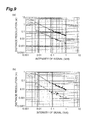
- Figs. 9(a) and 9(b) show diagrams representing the relationship between the radiation pulse width and the width of the imaging windows, and distance resolution.
- Fig. 9(a) represents a relationship between the intensity of radiation pulse and the distance resolution in a distance measurement performed every 30 frames per second. In the measurement, the width of radiation pulses of 100 ns or 0 ns was used.
- Fig. 9(b) represents a relationship between the intensity of radiation pulse and the distance resolution in a distance measurement performed every 3 frames per second. In the measurement, the width of radiation pulses of 100 ns or 0 ns was used.
- the distance resolution is enhanced as the intensity of the radiation pulse is increased.
- the width of the radiation pulse is changed from 100 ns to 10 ns, the distance resolution decreases to 1/10. Therefore, the distance resolution changes in proportion to the radiation pulse width; therefore, the distance resolution changes linearly with respect to the radiation pulse width from the radiation source as well as decreasing along with the radiation pulse width.
- the resolution values which were obtained from the experiments conducted by the inventor. Measuring method: radiation pulse 100ns, radiation pulse 10ns 30 frames per sec. 29 mm: 2.3 mm (without averaging process) 3 frames per sec., 9.1mm, 1.3mm, (with averaging process)
- Figs. 10(a) and 10(b) are diagrams representing an example of a measurement timing.
- the radiation source 13 provides 1st to n-th pulse trains (5 pulses in Figs. 10(a) and 10(b) ) P T1 to P T5 , which is irradiated as radiation pulses to an object in each of the 1st to n-th frames (5 frames in Figs. 10(a) and 10(b) ) arranged in order with respect to a time axis.
- the 1st to n-th frames are prescribed by control signals.
- each of the imaging times T PU1 to T PU5 is prescribed at a position of a predetermined time ⁇ T PD from the start point of the frame.
- Each frame includes the imaging windows A and B.
- the width of the pulses P T1 to P T5 is smaller than the width of the 1st and 2nd imaging windows. Alternatively, the width of the pulses P T1 to P T5 may be not more than the width of the 1st and 2nd imaging windows.
- Fig. 10(b) shows the start points of the five frames which are arranged in order with respect to a time axis as origin which are the start point of the respective frames (hereinafter, referred to as "reduced time axis").
- Fig. 10(b) illustrates that the 1st to n-th pulses P T1 to P T5 are shifted respectively by shift amounts different from each other, from the start point of the 1st to 5-th frames.
- 1st to n-th pulses P T1 to P T5 which are shifted by shift amounts different from each other, are used.
- the 1st to n-th pulses P T1 to P T5 are irradiated to the object from the 1st to n-th frames Frame 1 to Frame 5 which are arranged in order with respect to the time axis.
- the times-of-flight TOF1 to TOF5 can be measured plural times.
- Each of the 1st to n-th frames Frame 1 to Frame 5 includes a charge discarding window C different from the imaging windows A and B.
- a charge discarding window C different from the imaging windows A and B.
- the period of the charge discarding window C is used for reading the output signals S1 and S2 which are generated by the pixels in the imaging windows A and B.
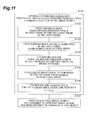
- Fig. 11 is a flowchart representing major steps in the method of generating an image signal S IMAGE by time-of-flight method using the pixel array 23 and the radiation source 13.
- step S101 using the detection element of the pixel array 23, 1 st to n-th imagings are carried out at the 1st to n-th times-of-flight TOF1 to TOFn different from each other to generatelst to n-th element image signals S E1 to S En .
- the 1st to n-th element image signals S E1 to S En are combined to generate an image signal S IMAGE including distance information concerning the object.
- step S101 includes the following steps.
- step S102 1st imaging is made using the imaging windows A and B in the 1st frame by emitting a 1st pulse in the 1st frame among the 1st to n-th frames which are arranged in order with respect to the time axis.
- step S103 a 1 st element image signal S E1 is generated by reading the 1 st image obtained in step S102 from the pixel array.
- step S104 in an i-th frame among the 2nd to n-th frames arranged in order with respect to the time axis, an i-th pulse is emitted to carry out i-th imaging by using the imaging windows A and B in the i-th frame.
- step S105 the i-th image obtained in step S104 is read from the pixel array to generate an i-th element image signal S Ei .
- step S 106 the i-th imaging and generation of the i-th element image signal S Ei are repeated.
- the 1st to n-th pulses which are shifted by shift amounts different from each other, are used. These pulses are irradiated to the object respectively in the 1st to n-th frames arranged in order with respect to the time axis.
- Plural times of measurement of the times-of-flight TOF1 to TOFn can be made by associating each of the 1st to n-th pulses with the 1st and 2nd imaging windows respectively in the 1 st to n-th frames.
- each of the times-of-flight covers distance measuring ranges different from each other. Also, since the element image signals S E1 to S En are generated at n imaging timings corresponding to the times-of-flight TOF1 to TOFn, each of the element image signals S E1 to S En has distance information of the object in distance ranges different from each other. Since the image signal S IMAGE is generated by combining these element image signals S E1 to S En , the distance information of the object can be obtained in a wide distance range.
- 1 st and 2nd signals S1 and S2 responding to the incident radiation entering the detection element of the pixel are generated in the imaging windows A and B, and by plural times of time-of-flight measurement, the distance range information concerning the object is obtained in desired distance range. Therefore, the width of the radiation pulses does not have to be increased to obtain distance information of an object in a wide distance range. Accordingly, the distance resolution is not reduced in each time-of-flight measurement.
- the radiation source 13 provides a single pulse P T0 as a radiation pulse to a single frame Frame0.
- Fig. 12(a) represents timings in which single frame is used. The frame is prescribed by control signals.
- the 1st to n-th imaging timings in the 1st to n-th frames (in this example, T PU1 , T PU2, and T PU3 ) are set within the single frame Frame0.
- the imaging times T PU1 , T PU2 and T PU3 of the imaging timings are shifted from the start point of the single frame Frame0 by shift amounts different from each other.
- a window corresponding to the incident radiation entering the detection element is prescribed for taking electric charge to the floating semiconductor area.
- the imaging window A is provided; and immediately after each of the imaging times, the imaging window B is provided. Therefore, the windows between these imaging windows are used as common imaging windows A and B.
- the imaging windows A and B are arranged alternately to constitute a row of the imaging windows.
- a single pickup window A is set; and at the last thereof, a single imaging window B is set.
- one or a plurality of common imaging windows are set between the 1st single imaging window and the 2nd single imaging window.
- the common imaging windows are provided for both of the 1st imaging window and the 2nd imaging window. Therefore, before and after the imaging time in each of the 1st to n-th imaging timings, 1st and 2nd imaging windows are provided. At the plurality of imaging times in the row of the imaging windows, a plurality of element image signals is generated.
- the duration of the single pulse P T0 is equal to that of the 1st imaging window A; and the duration of the single pulse P T0 is equal to the period of the 2nd imaging window B.
- the duration of the single pulse P T0 is prescribed from the start point of the frame Frame0. From the end point of the single pulse P T0 , a row of a predetermined number of windows is prescribed. Windows within a window row are prescribed by the turn-on of the transfer gates TXi different from each other.
- the single frame Frame0 includes a charge discarding window with a period different from the period of the row of the windows.
- the pixel 27 discards the electric charge of the detection element through the charge discarding window. With this arrangement, background noises affecting the detection element are removed.
- Fig. 13 is a plan view illustrating a structure of a pixel applicable to this embodiment. Comparing the pixel in Fig. 13 to that in Fig. 3(a) , the structure of the pixel in Fig. 13 is identical to that of the pixel in Fig. 3(a) excepting the structure of the transfer gate.
- the pixel in Fig. 13 includes the 1st to j-th transfer gates (TX1 and TX3 in Fig. 13 ) in a first group, which are disposed at the one side of the photogate PG, and the (j+1)-th to (n+1)-th transfer gates (TX2 and TX4 in Fig. 13 ) in a second group, which are disposed at the other side of the photogate PG.
- the 1st to (n+1)-th transfer gates (TX1 to TX4 in Fig. 13 ) are turned on at any of the 1st to n-th imaging timings.
- Each of the 1st to (n+1)-th transfer gates (TX1 to TX4 in Fig. 13 ) is connected to one of the 1st to (n+1)-th floating semiconductor areas (FD1 to FD4 in Fig. 13 ).
- the photogate PG is located between the discard gates TX BCD .
- Fig. 12(b) represents the signals which are generated by the selection gates TX1 to TX4 responding to the delay of pulse.
- the reference of the delay time is prescribed by the rising time of the radiation pulse.
- the selection gates TX1 to TX4 take in a pulse delayed due to times-of-flight and generates signals V TX1 , V TX2 , V TX3 and V TX4 shown in Fig. 12(b).
- Fig. 12(b) illustrates that the transfer gates TX1 to TX4 generate signals different from each other responding to the delay time.
- Fig. 12(b) illustrates characteristics corresponding to those in Fig. 7(b) and Fig. 8(b) .
- one single pulse T P0 is used, but the time-of-flight measurement can be made plural times by using three or more rows of the imaging windows. During the imaging period, one of the transfer gates TX1 to TX4 is turned on.
- Fig. 14 is a flowchart representing major steps in the method of generating an image signal S IMAGE by time-of-flight method using the pixel array 23 and the radiation source 13.
- step S201 n-times of imaging is made by times-of-flight TOF1 to TOFn, which are different from each other, using the detection element of the pixel array 23 to generate element image signals S E1 to S En .
- step S208 element image signals S E1 to S En are combined to generate an image signal S IMAGE .
- step S201 includes the following steps.
- step S202 radiation pulses are irradiated to the object to measure the time-of-flight.
- step S203 1st imaging is made in the 1st imaging window within the plurality of window rows.
- step S204 the 1st image obtained in step S203 is read from the pixel array to generate a 1st element image signal S E1 .
- step S205 i-th imaging is made in the i-th imaging window immediately after the (i-1)-th window.
- step S206 the i-th image obtained in step S205 is read from the pixel array to generate a 1st element image signal S Ei .
- step S207 the i-th imaging and the generation of i-th element image signal S Ei are repeated.
- the imaging is made plural times using a single radiation pulse and three or more imaging windows.
- the times-of-flight TOF1 to TOFn are different from each other, different measurement ranges are covered by the different times-of-flight.
- the element image signals S E1 to S En are generated at n-times of imaging timings corresponding to the times-of-flight TOF1 to TOFn, each of the element image signals S E1 to S En has different distance information of the object in distance ranges different from each other. Since these element image signals S E1 to S En are combined to generate the image signal S IMAGE , distance information of the object can be obtained in a wide distance range.
- the 1st and 2nd output signals S1 and S2 which correspond to the incident radiation entering the detection element of the pixel, are generated by the imaging window A and the imaging window B at the 1st to n-th imaging timings, distance range information concerning the object is obtained in a desired range by plural times of time-of-flight measurement. Accordingly, the width of radiation pulse does not have to be increased to obtain distance information of the object in a wide distance range. Therefore, the distance resolution is not reduced in each time-of-flight measurement.
- frames Frame 1 to Frame 4 are disposed along the time axis.
- Each of the frames Frame 1 to Frame 4 is provided with imaging windows A and B.
- the width of the imaging windows A and B is 100 nanoseconds; the imaging window A is disposed being adjusted to the start point of the frame, and the imaging window B is disposed immediately after the imaging window A.
- the frames Frame 1 to Frame 4 are provided with pulses P T1 to P T4 respectively.
- the width of the pulse P T for time-of-flight is 25 nanoseconds.
- the pulse P T1 is shifted by a shift amount of 75 nanoseconds from the start point of the frame Frame 1; the pulse P T2 is shifted by a shift amount of 50 nanoseconds from the start point of the frame Frame 2; pulse P T3 is shifted by a shift amount of 25 nanoseconds from the start point of the frame Frame 3; and the pulse P T4 is provided to the start point of the frame Frame 4.
- the measurement range is 3.75 m.
- the frame Frame 1 a range of 3.75 m from the sensor can be measured; when the frame Frame 2 is used, a range of from 3.75 m to 7.5m can be measured;when the frame Frame 3 is used, a range of from 7.5 m to 11.25 m can be measured; and when the frame Frame 4 is used, a range of from 11.25 m to 15 m can be measured.
- the measurement range is 15 m that is the same as the measurement range using a pulse width of 100 nanoseconds.
- the distance image sensor since the pulse width can be reduced, compared to the distance measurement using the pulse width of 100 nanoseconds, the distance resolution is enhanced.
- the width of the pulse P T is 100 nanoseconds (comparative example)
- electron (N B ) generated by photogate responding to background light was 10 4 , 10 5
- the distance resolution ⁇ L is 0.040 m, 0.045 m respectively.
- the width of the pulse P T was 25 nanoseconds
- electron (N B ) generated by the photogate responding to background light was 10 4 , 10 5
- the distance resolution ⁇ L was 0.010 m, 0.011 m respectively.
- frames Frame 1 to Frame 4 are arranged along the time axis.
- Each of the frames Frame 1 to Frame 4 is provided with imaging windows A and B.
- the width of the imaging windows A and B is 25 nanoseconds; the imaging window A is disposed at a time shifted by 75 nanoseconds from the start point of the frame, and the imaging window B is disposed immediately after imaging window A.
- the frames Frame 1 to Frame 4 are provided with pulses P T1 to P T4 respectively as same as Example 1.
- the inventor estimated the resolution in the distance measurement as shown in Fig. 16(b) .
- electron number (N R ) due to random noise on the readout circuit and electron (N B ) which is generated by the photogate responding to the background light is 100, 10 5 respectively, and when the duty ratio of the pulses of the light source is 0.1, the distance resolution of the distance image sensor of the pulse P T of 100 nanoseconds (comparative example) was estimated.
- the distance resolution ⁇ L was approximate 4.5 cm or less with respect to the measuring range of 15 m.
- the distance resolution of the distance image sensor with a pulse P T of 25 nanoseconds was estimated.
- the distance resolution ⁇ L was approx. 1.1 cm or less, 1 cm or less, respectively, with respect to the distance measurement range of 15 m.
- frames Frame 1 to Frame 7 are arranged along the time axis.
- the frames Frame1 to Frame 7 are provided with imaging windows A and B.
- the width of the imaging windows A and B is 100 nanoseconds; the imaging window A is disposed being aligned with the start point of the frame; and the imaging window B is disposed immediately after the imaging window A.
- the frames Frame 1 to Frame 7 are provided with pulses P T1 to P T7 as same as Example 1.
- the width of the imaging windows A and B is 100 nanoseconds, and the width of pulses P T1 to P T7 for time-of-flight is 25 nanoseconds.
- the delay time of the signals from the pixel displaced from the linear change with respect to the delay time near 0 second and 10 nanoseconds.
- This non-linearity reduces the distance accuracy.
- the distance accuracy can be maintained to a predetermined value.
- the width and the shift amount of the pulses P T1 to P T7 the distance can be determined based on the relationship between the delay time and the distance using linear area of each of the pulses P T1 to P T7 .
- the pulse P T1 is provided crossing the changing time between the imaging window A and the imaging window B.
- the falling of the pulse P T2 is shifted by +3 nanoseconds from the time as reference.
- the pulse P T2 is shifted by a shift amount of -4 nanoseconds with respect to the shift amount of the pulse P T1 .
- the pulse P T3 is shifted by a shift amount of -4 nanoseconds with respect to the shift amount of the pulse P T2 .
- the pulses P T4 to P T7 are also shifted by a predetermined adjustment amount (-4 nanoseconds) with respect to the shift amount of the pulses P T3 to P T6 in the neighboring frames as reference. Therefore, the difference between the shift amount of the radiation pulse in a frame and the shift amount of the radiation pulse in the neighboring frame is smaller than the width of the radiation pulse.
- the distance image sensor since the linear response area is used, distance accuracy is ensured in entire time-of-flight measurement range.
- embodiments of the invention relate to TOF distance image sensor and method based on range shift operation, and are constituted as described below.
- small duty ratio i. e. short period pulsed light
- generated electric charge is discarded without being accumulated.
- the imaging is made plural times while shifting the relative relationship between the emitting radiation timing of the light pulse and the imaging windows to generate a plurality of element image signals. By combining these element image signals, a desired distance resolution is ensured and the distance measurement range can be increased.
- the distance image sensor having the structure for discarding electric charge carries out the imaging while shifting the relative relationship between the emitting timing of short-period light pulse and the imaging windows for the imaging.
- the images are combined and used for distance measurement. With this, while maintaining high distance resolution, a wide distance measurement range is ensured.
- the distance image sensor and method according to the embodiment read the signals from the pixel at every timing of a plurality of imaging timings by using prescribed imaging windows. With this arrangement, as the signals within one frame, a plurality of element image signals, the ranges of which are shifted by a different value from each other, are read out.
- the distance image sensor and method according to the embodiment use a plurality of distance measurement ranges which are shifted so as to have shift amounts different from each other and carry out the measurement of the distance using distance measurement pulses which are arranged so that the distance measurement ranges are overlapped with each other. Distance measurement ranges different from each other are allotted to each distance measurement using the pulses, and the pulses are adjusted so that the difference of the shift amount among the distance measurement pulses is smaller than the pulse width of the distance measurement pulses. With this arrangement, the measurement can be made linearly in a wide measurement range.
Landscapes
- Engineering & Computer Science (AREA)
- Physics & Mathematics (AREA)
- Electromagnetism (AREA)
- Computer Networks & Wireless Communication (AREA)
- General Physics & Mathematics (AREA)
- Radar, Positioning & Navigation (AREA)
- Remote Sensing (AREA)
- Multimedia (AREA)
- Signal Processing (AREA)
- Optical Radar Systems And Details Thereof (AREA)
- Solid State Image Pick-Up Elements (AREA)
- Transforming Light Signals Into Electric Signals (AREA)
Applications Claiming Priority (2)
| Application Number | Priority Date | Filing Date | Title |
|---|---|---|---|
| JP2008196616A JP5585903B2 (ja) | 2008-07-30 | 2008-07-30 | 距離画像センサ、及び撮像信号を飛行時間法により生成する方法 |
| PCT/JP2009/063582 WO2010013779A1 (fr) | 2008-07-30 | 2009-07-30 | Capteur d'image de distance et procédé pour générer un signal d'image par le procédé de temps de vol |
Publications (3)
| Publication Number | Publication Date |
|---|---|
| EP2322953A1 true EP2322953A1 (fr) | 2011-05-18 |
| EP2322953A4 EP2322953A4 (fr) | 2012-01-25 |
| EP2322953B1 EP2322953B1 (fr) | 2013-01-30 |
Family
ID=41610477
Family Applications (1)
| Application Number | Title | Priority Date | Filing Date |
|---|---|---|---|
| EP09803021A Active EP2322953B1 (fr) | 2008-07-30 | 2009-07-30 | Capteur d'image de distance et procédé pour générer un signal d'image par le procédé de temps de vol |
Country Status (5)
| Country | Link |
|---|---|
| US (1) | US8537218B2 (fr) |
| EP (1) | EP2322953B1 (fr) |
| JP (1) | JP5585903B2 (fr) |
| KR (1) | KR101508410B1 (fr) |
| WO (1) | WO2010013779A1 (fr) |
Cited By (24)
| Publication number | Priority date | Publication date | Assignee | Title |
|---|---|---|---|---|
| BE1020078A3 (fr) * | 2011-07-15 | 2013-04-02 | Softkinetic Sensors Nv | Procede et appareil de prise de vues a technique du temps de vol pour fournir des informations de distance. |
| EP2290393A3 (fr) * | 2009-08-14 | 2013-05-08 | Fraunhofer-Gesellschaft zur Förderung der angewandten Forschung e.V. | Concept de mesure optique de distance |
| US20130235160A1 (en) * | 2012-03-06 | 2013-09-12 | Microsoft Corporation | Optical pulse shaping |
| CN104914446A (zh) * | 2015-06-19 | 2015-09-16 | 南京理工大学 | 基于光子计数的三维距离图像时域实时去噪方法 |
| EP3159711A1 (fr) * | 2015-10-23 | 2017-04-26 | Xenomatix NV | Système et procédé pour mesurer une distance par rapport à un objet |
| EP3301477A1 (fr) | 2016-10-03 | 2018-04-04 | Xenomatix NV | Système de télémétrie d'un objet |
| EP3301479A1 (fr) | 2016-10-03 | 2018-04-04 | Xenomatix NV | Procédé d'atténuation d'éclairage d'arrière-plan à partir d'une valeur d'exposition d'un pixel dans une mosaïque, et pixel pour une utilisation dans celle-ci |
| EP3301478A1 (fr) | 2016-10-03 | 2018-04-04 | Xenomatix NV | Système de détermination d'une distance par rapport à un objet |
| EP3301480A1 (fr) | 2016-10-03 | 2018-04-04 | Xenomatix NV | Système et procédé pour mesurer une distance par rapport à un objet |
| CN108430851A (zh) * | 2015-12-24 | 2018-08-21 | Lg 电子株式会社 | 夜间图像显示装置及其图像处理方法 |
| WO2019115839A1 (fr) | 2017-12-15 | 2019-06-20 | Xenomatix Nv | Système et procédé de détermination de la distance d'un objet |
| EP3550329A1 (fr) | 2018-04-04 | 2019-10-09 | Xenomatix NV | Système et procédé pour mesurer une distance par rapport à un objet |
| CN111226434A (zh) * | 2017-10-20 | 2020-06-02 | 国立大学法人静冈大学 | 距离图像测定装置以及距离图像测定方法 |
| US10764518B2 (en) | 2017-04-23 | 2020-09-01 | Xenomatix Nv | Pixel structure |
| WO2021113001A1 (fr) * | 2019-12-03 | 2021-06-10 | Apple Inc. | Réseau configurable de détecteurs de photon unique |
| US11371833B2 (en) | 2019-02-11 | 2022-06-28 | Apple Inc. | Calibration of depth sensing using a sparse array of pulsed beams |
| US11415679B2 (en) | 2015-08-20 | 2022-08-16 | Apple Inc. | SPAD array with gated histogram construction |
| US11500094B2 (en) | 2019-06-10 | 2022-11-15 | Apple Inc. | Selection of pulse repetition intervals for sensing time of flight |
| US11555900B1 (en) | 2019-07-17 | 2023-01-17 | Apple Inc. | LiDAR system with enhanced area coverage |
| US11681027B2 (en) | 2017-06-29 | 2023-06-20 | Apple Inc. | Time-of-flight depth mapping with parallax compensation |
| US11681028B2 (en) | 2021-07-18 | 2023-06-20 | Apple Inc. | Close-range measurement of time of flight using parallax shift |
| US11852727B2 (en) | 2017-12-18 | 2023-12-26 | Apple Inc. | Time-of-flight sensing using an addressable array of emitters |
| US11874374B2 (en) | 2016-12-30 | 2024-01-16 | Xenomatix Nv | System for characterizing surroundings of a vehicle |
| US11992192B2 (en) | 2018-07-23 | 2024-05-28 | Olympus Corporation | Endoscope apparatus |
Families Citing this family (57)
| Publication number | Priority date | Publication date | Assignee | Title |
|---|---|---|---|---|
| KR101666020B1 (ko) | 2010-06-25 | 2016-10-25 | 삼성전자주식회사 | 깊이 영상 생성 장치 및 그 방법 |
| JP5518667B2 (ja) * | 2010-10-12 | 2014-06-11 | 浜松ホトニクス株式会社 | 距離センサ及び距離画像センサ |
| GB2486208A (en) | 2010-12-06 | 2012-06-13 | Melexis Tessenderlo Nv | Demodulation sensor and method for detection and demodulation of temporarily modulated electromagnetic fields for use in Time of Flight applications. |
| JP5829036B2 (ja) | 2011-03-31 | 2015-12-09 | 本田技研工業株式会社 | 単位画素の信号加算方法 |
| JP5635938B2 (ja) | 2011-03-31 | 2014-12-03 | 本田技研工業株式会社 | 固体撮像装置 |
| JP5635937B2 (ja) | 2011-03-31 | 2014-12-03 | 本田技研工業株式会社 | 固体撮像装置 |
| JP5660959B2 (ja) | 2011-03-31 | 2015-01-28 | 本田技研工業株式会社 | 受光装置 |
| JP2013076645A (ja) * | 2011-09-30 | 2013-04-25 | Stanley Electric Co Ltd | 距離画像生成装置および距離画像生成方法 |
| KR101863626B1 (ko) | 2011-11-02 | 2018-07-06 | 삼성전자주식회사 | 영상 처리 장치 및 방법 |
| US8642938B2 (en) | 2012-01-13 | 2014-02-04 | Omnivision Technologies, Inc. | Shared time of flight pixel |
| US8686367B2 (en) | 2012-03-01 | 2014-04-01 | Omnivision Technologies, Inc. | Circuit configuration and method for time of flight sensor |
| US10324033B2 (en) | 2012-07-20 | 2019-06-18 | Samsung Electronics Co., Ltd. | Image processing apparatus and method for correcting an error in depth |
| US9786252B2 (en) | 2012-09-10 | 2017-10-10 | Samsung Electronics Co., Ltd. | Method and apparatus for suppressing background light in time of flight sensor |
| FR2998683B1 (fr) * | 2012-11-27 | 2016-01-15 | Saint Louis Inst | Procede d imagerie 3d |
| JP6025081B2 (ja) * | 2013-02-28 | 2016-11-16 | 株式会社テクノロジーハブ | 距離画像センサ |
| US9134114B2 (en) | 2013-03-11 | 2015-09-15 | Texas Instruments Incorporated | Time of flight sensor binning |
| KR102007277B1 (ko) | 2013-03-11 | 2019-08-05 | 삼성전자주식회사 | 3차원 이미지 센서의 거리 픽셀 및 이를 포함하는 3차원 이미지 센서 |
| US10216266B2 (en) * | 2013-03-14 | 2019-02-26 | Qualcomm Incorporated | Systems and methods for device interaction based on a detected gaze |
| US9204143B2 (en) | 2013-03-15 | 2015-12-01 | Samsung Electronics Co., Ltd. | Image sensor, operation method thereof, and system including the same |
| JP6176777B2 (ja) * | 2013-03-25 | 2017-08-09 | 国立大学法人静岡大学 | 画素回路及び撮像素子 |
| KR102061699B1 (ko) | 2013-06-19 | 2020-01-02 | 삼성전자주식회사 | 이미지 센서, 이를 포함하는 이미지 처리 시스템 및 이의 동작 방법 |
| CN103412314B (zh) * | 2013-08-01 | 2015-07-29 | 清华大学 | 一种基于天体辐射信号相干性的成像方法 |
| JP2015043488A (ja) * | 2013-08-26 | 2015-03-05 | 清水建設株式会社 | 遠隔操作装置及びそれを用いた遠隔施工方法 |
| US9182490B2 (en) | 2013-11-27 | 2015-11-10 | Semiconductor Components Industries, Llc | Video and 3D time-of-flight image sensors |
| US10230914B2 (en) | 2014-02-07 | 2019-03-12 | National University Corporation Shizuoka University | Charge modulation element and solid-state imaging device |
| JP6320154B2 (ja) * | 2014-04-25 | 2018-05-09 | キヤノン株式会社 | 撮像装置及び撮像装置の駆動方法 |
| US9523765B2 (en) * | 2014-07-14 | 2016-12-20 | Omnivision Technologies, Inc. | Pixel-level oversampling for a time of flight 3D image sensor with dual range measurements |
| JP6520053B2 (ja) * | 2014-11-06 | 2019-05-29 | 株式会社デンソー | 光飛行型測距装置 |
| JP6539990B2 (ja) * | 2014-11-14 | 2019-07-10 | 株式会社デンソー | 光飛行型測距装置 |
| US10422879B2 (en) | 2014-11-14 | 2019-09-24 | Denso Corporation | Time-of-flight distance measuring device |
| JP6424581B2 (ja) * | 2014-11-21 | 2018-11-21 | 株式会社デンソー | 光飛行型測距装置 |
| US20160290790A1 (en) * | 2015-03-31 | 2016-10-06 | Google Inc. | Method and apparatus for increasing the frame rate of a time of flight measurement |
| JP6406449B2 (ja) * | 2015-06-24 | 2018-10-17 | 株式会社村田製作所 | 距離センサ |
| JP6651720B2 (ja) * | 2015-07-10 | 2020-02-19 | 株式会社ニコン | 撮像素子および撮像装置 |
| EP3379291A4 (fr) * | 2015-11-16 | 2018-12-05 | Panasonic Intellectual Property Management Co., Ltd. | Dispositif d'imagerie et élément d'imagerie à semi-conducteurs utilisé dans ce dernier |
| FR3043797A1 (fr) * | 2015-11-16 | 2017-05-19 | Stmicroelectronics (Grenoble 2) Sas | |
| FR3043796A1 (fr) | 2015-11-16 | 2017-05-19 | Stmicroelectronics (Grenoble 2) Sas | |
| WO2017098725A1 (fr) | 2015-12-08 | 2017-06-15 | パナソニックIpマネジメント株式会社 | Dispositif d'imagerie à état solide, dispositif de mesure de distance et procédé de mesure de distance |
| EP3414599B1 (fr) | 2016-02-08 | 2019-12-18 | Denso Corporation | Dispositif de mesure de distance par temps de vol et procédé de détection d'erreur multivoie |
| WO2017138032A1 (fr) | 2016-02-08 | 2017-08-17 | Denso Corporation | Dispositif de mesure de distance par temps de vol et procédé de détection d'erreur multivoie |
| EP3418772A4 (fr) | 2016-02-17 | 2019-03-13 | Panasonic Intellectual Property Management Co., Ltd. | Dispositif de mesure de distance |
| US10291895B2 (en) | 2016-10-25 | 2019-05-14 | Omnivision Technologies, Inc. | Time of flight photosensor |
| JP6735515B2 (ja) * | 2017-03-29 | 2020-08-05 | パナソニックIpマネジメント株式会社 | 固体撮像装置 |
| JP2018185179A (ja) * | 2017-04-25 | 2018-11-22 | 株式会社リコー | 測距装置、監視装置、3次元計測装置、移動体、ロボット及び測距方法 |
| US11442169B2 (en) | 2017-08-08 | 2022-09-13 | National University Corporation Shizuoka University | Distance-image-measuring apparatus and distance-image-measuring method |
| US20190187256A1 (en) * | 2017-12-19 | 2019-06-20 | Samsung Electronics Co., Ltd. | Non-spad pixels for direct time-of-flight range measurement |
| TWI801572B (zh) * | 2018-07-24 | 2023-05-11 | 南韓商三星電子股份有限公司 | 影像感測器、成像單元及生成灰階影像的方法 |
| US11294039B2 (en) * | 2018-07-24 | 2022-04-05 | Samsung Electronics Co., Ltd. | Time-resolving image sensor for range measurement and 2D greyscale imaging |
| JP2022020871A (ja) * | 2018-12-06 | 2022-02-02 | パナソニックIpマネジメント株式会社 | 物体認識装置、物体認識方法、およびプログラム |
| JP7531140B2 (ja) * | 2018-12-06 | 2024-08-09 | パナソニックIpマネジメント株式会社 | 距離情報取得装置、距離情報取得方法、およびプログラム |
| KR102646902B1 (ko) * | 2019-02-12 | 2024-03-12 | 삼성전자주식회사 | 거리 측정을 위한 이미지 센서 |
| CN110276286B (zh) * | 2019-06-13 | 2022-03-04 | 中国电子科技集团公司第二十八研究所 | 一种基于tx2的嵌入式全景视频拼接系统 |
| US20220357445A1 (en) | 2019-06-25 | 2022-11-10 | National University Corporation Shizuoka University | Distance image measuring device |
| KR20210055821A (ko) | 2019-11-07 | 2021-05-18 | 삼성전자주식회사 | 깊이의 측정 범위에 기초하여 동작하는 센서 및 이를 포함하는 센싱 시스템 |
| KR20220009223A (ko) | 2020-07-15 | 2022-01-24 | 삼성전자주식회사 | 멀티-탭 구조를 갖는 거리 픽셀 및 이를 포함하는 비행 거리 센서 |
| KR20220018215A (ko) * | 2020-08-06 | 2022-02-15 | 삼성전자주식회사 | 비행 거리 센서 및 비행 거리 센서의 거리 측정 방법 |
| WO2023199979A1 (fr) * | 2022-04-13 | 2023-10-19 | 凸版印刷株式会社 | Dispositif de capture d'image de distance et procédé de capture d'image de distance |
Citations (3)
| Publication number | Priority date | Publication date | Assignee | Title |
|---|---|---|---|---|
| US20020149694A1 (en) * | 2001-04-16 | 2002-10-17 | Asahi Kogaku Kogyo Kabushiki Kaisha | Three-dimensional image capturing device |
| WO2005076037A1 (fr) * | 2004-02-04 | 2005-08-18 | Elbit Systems Ltd. | Synchronisation d'image |
| WO2008152647A2 (fr) * | 2007-06-15 | 2008-12-18 | Ben Gurion University Of The Negev Research And Development Authority | Procédé et appareil d'imagerie tridimensionnelle |
Family Cites Families (10)
| Publication number | Priority date | Publication date | Assignee | Title |
|---|---|---|---|---|
| KR900019510A (ko) * | 1989-05-31 | 1990-12-24 | 강진구 | 디지탈 화상처리장치에 있어서 신호지연 조정방식 |
| DE4440613C1 (de) | 1994-11-14 | 1996-07-25 | Leica Ag | Vorrichtung und Verfahren zur Detektion und Demodulation eines intensitätsmodulierten Strahlungsfeldes |
| JPH09178853A (ja) * | 1995-12-25 | 1997-07-11 | Hitachi Ltd | イメージングレーザー測距装置 |
| DE69729648T2 (de) | 1996-01-22 | 2005-06-09 | California Institute Of Technology, Pasadena | Aktivpixelsensormatrix mit mehrfachauflösungsausgabe |
| US5986297A (en) | 1996-05-22 | 1999-11-16 | Eastman Kodak Company | Color active pixel sensor with electronic shuttering, anti-blooming and low cross-talk |
| JP3874135B2 (ja) | 1997-12-05 | 2007-01-31 | 株式会社ニコン | 固体撮像素子 |
| US6323942B1 (en) | 1999-04-30 | 2001-11-27 | Canesta, Inc. | CMOS-compatible three-dimensional image sensor IC |
| EP1423731B1 (fr) * | 2001-08-06 | 2006-10-04 | Siemens Aktiengesellschaft | Procede et dispositif pour acquerir une image telemetrique tridimensionnelle |
| JP4280822B2 (ja) | 2004-02-18 | 2009-06-17 | 国立大学法人静岡大学 | 光飛行時間型距離センサ |
| US7781811B2 (en) * | 2005-08-30 | 2010-08-24 | National University Corporation Shizuoka University | Semiconductor range-finding element and solid-state imaging device |
-
2008
- 2008-07-30 JP JP2008196616A patent/JP5585903B2/ja active Active
-
2009
- 2009-07-30 KR KR1020117002911A patent/KR101508410B1/ko active IP Right Grant
- 2009-07-30 WO PCT/JP2009/063582 patent/WO2010013779A1/fr active Application Filing
- 2009-07-30 US US13/056,697 patent/US8537218B2/en active Active
- 2009-07-30 EP EP09803021A patent/EP2322953B1/fr active Active
Patent Citations (3)
| Publication number | Priority date | Publication date | Assignee | Title |
|---|---|---|---|---|
| US20020149694A1 (en) * | 2001-04-16 | 2002-10-17 | Asahi Kogaku Kogyo Kabushiki Kaisha | Three-dimensional image capturing device |
| WO2005076037A1 (fr) * | 2004-02-04 | 2005-08-18 | Elbit Systems Ltd. | Synchronisation d'image |
| WO2008152647A2 (fr) * | 2007-06-15 | 2008-12-18 | Ben Gurion University Of The Negev Research And Development Authority | Procédé et appareil d'imagerie tridimensionnelle |
Non-Patent Citations (4)
| Title |
|---|
| See also references of WO2010013779A1 * |
| SHOJI KAWAHITO ET AL: "A CMOS Time-of-Flight Range Image Sensor With Gates-on-Field-Oxide Structure", IEEE SENSORS JOURNAL, IEEE SERVICE CENTER, NEW YORK, NY, US, vol. 7, no. 12, 1 December 2007 (2007-12-01), pages 1578-1586, XP011196172, ISSN: 1530-437X, DOI: 10.1109/JSEN.2007.907561 * |
| STOPPA D ET AL: "A 16xl6-pixel range-finding CMOS image sensor", SOLID-STATE CIRCUITS CONFERENCE, 2004. ESSCIRC 2004. PROCEEDING OF THE 30TH EUROPEAN, IEEE, PISCATAWAY, NJ, USA, 21 September 2004 (2004-09-21), pages 419-422, XP010740129, DOI: 10.1109/ESSCIR.2004.1356707 ISBN: 978-0-7803-8480-4 * |
| TOMONARI SAWADA ET AL: "TOF range image sensor using a range-shift technique", 2008 IEEE SENSORS,LECCE, ITALY, IEEE, PISCATAWAY, NJ, USA, 26 October 2008 (2008-10-26), pages 1390-1393, XP031375344, ISBN: 978-1-4244-2580-8 * |
Cited By (45)
| Publication number | Priority date | Publication date | Assignee | Title |
|---|---|---|---|---|
| EP2290393A3 (fr) * | 2009-08-14 | 2013-05-08 | Fraunhofer-Gesellschaft zur Förderung der angewandten Forschung e.V. | Concept de mesure optique de distance |
| US8792087B2 (en) | 2009-08-14 | 2014-07-29 | Fraunhofer-Gesellschaft Zur Foerderung Der Angewandten Forschung E.V. | Concept for optical distance measurement |
| BE1020078A3 (fr) * | 2011-07-15 | 2013-04-02 | Softkinetic Sensors Nv | Procede et appareil de prise de vues a technique du temps de vol pour fournir des informations de distance. |
| US20130235160A1 (en) * | 2012-03-06 | 2013-09-12 | Microsoft Corporation | Optical pulse shaping |
| CN104914446B (zh) * | 2015-06-19 | 2017-06-27 | 南京理工大学 | 基于光子计数的三维距离图像时域实时去噪方法 |
| CN104914446A (zh) * | 2015-06-19 | 2015-09-16 | 南京理工大学 | 基于光子计数的三维距离图像时域实时去噪方法 |
| US11415679B2 (en) | 2015-08-20 | 2022-08-16 | Apple Inc. | SPAD array with gated histogram construction |
| WO2017068199A1 (fr) | 2015-10-23 | 2017-04-27 | Xenomatix Nv | Système et procédé de détermination d'une distance par rapport à un objet |
| US10921454B2 (en) | 2015-10-23 | 2021-02-16 | Xenomatix Nv | System and method for determining a distance to an object |
| EP3159711A1 (fr) * | 2015-10-23 | 2017-04-26 | Xenomatix NV | Système et procédé pour mesurer une distance par rapport à un objet |
| CN108430851A (zh) * | 2015-12-24 | 2018-08-21 | Lg 电子株式会社 | 夜间图像显示装置及其图像处理方法 |
| CN108430851B (zh) * | 2015-12-24 | 2021-03-09 | Lg 电子株式会社 | 夜间图像显示装置及其图像处理方法 |
| US10830891B2 (en) | 2015-12-24 | 2020-11-10 | Lg Electronics Inc. | Night image display apparatus and image processing method thereof |
| EP3395636A4 (fr) * | 2015-12-24 | 2019-07-24 | LG Electronics Inc. -1- | Appareil d'affichage d'image nocturne et son procédé de traitement d'image |
| EP3301480A1 (fr) | 2016-10-03 | 2018-04-04 | Xenomatix NV | Système et procédé pour mesurer une distance par rapport à un objet |
| EP3789792A1 (fr) | 2016-10-03 | 2021-03-10 | Xenomatix NV | Procédé d'atténuation d'éclairage d'arrière-plan à partir d'une valeur d'exposition d'un pixel dans une mosaïque, et pixel pour une utilisation dans celle-ci |
| WO2018065429A1 (fr) | 2016-10-03 | 2018-04-12 | Xenomatix Nv | Système et procédé de détermination d'une distance par rapport à un objet |
| US11513199B2 (en) | 2016-10-03 | 2022-11-29 | Xenomatix Nv | System and method for determining a distance to an object |
| WO2018065427A1 (fr) | 2016-10-03 | 2018-04-12 | Xenomatix Nv | Système de détermination d'une distance par rapport à un objet |
| US11543501B2 (en) | 2016-10-03 | 2023-01-03 | Xenomatix Nv | Method for subtracting background light from an exposure value of a pixel in an imaging array, and pixel for use in same |
| US11029391B2 (en) | 2016-10-03 | 2021-06-08 | Xenomatix Nv | System for determining a distance to an object |
| EP3301477A1 (fr) | 2016-10-03 | 2018-04-04 | Xenomatix NV | Système de télémétrie d'un objet |
| WO2018065428A2 (fr) | 2016-10-03 | 2018-04-12 | Xenomatix Nv | Système de détermination d'une distance par rapport à un objet |
| WO2018065426A1 (fr) | 2016-10-03 | 2018-04-12 | Xenomatix Nv | Procédé pour soustraire une lumière d'arrière-plan d'une valeur d'exposition d'un pixel dans un réseau d'imagerie, et pixel destiné à être utilisé dans celui-ci |
| US10852400B2 (en) | 2016-10-03 | 2020-12-01 | Xenomatix Nv | System for determining a distance to an object |
| EP3301478A1 (fr) | 2016-10-03 | 2018-04-04 | Xenomatix NV | Système de détermination d'une distance par rapport à un objet |
| EP3301479A1 (fr) | 2016-10-03 | 2018-04-04 | Xenomatix NV | Procédé d'atténuation d'éclairage d'arrière-plan à partir d'une valeur d'exposition d'un pixel dans une mosaïque, et pixel pour une utilisation dans celle-ci |
| US11874374B2 (en) | 2016-12-30 | 2024-01-16 | Xenomatix Nv | System for characterizing surroundings of a vehicle |
| US10764518B2 (en) | 2017-04-23 | 2020-09-01 | Xenomatix Nv | Pixel structure |
| US11681027B2 (en) | 2017-06-29 | 2023-06-20 | Apple Inc. | Time-of-flight depth mapping with parallax compensation |
| CN111226434A (zh) * | 2017-10-20 | 2020-06-02 | 国立大学法人静冈大学 | 距离图像测定装置以及距离图像测定方法 |
| CN111226434B (zh) * | 2017-10-20 | 2022-05-31 | 国立大学法人静冈大学 | 距离图像测定装置以及距离图像测定方法 |
| US11405577B2 (en) | 2017-10-20 | 2022-08-02 | National University Corporation Shizuoka University | Distance image measurement device and distance image measurement method |
| US10768301B2 (en) | 2017-12-15 | 2020-09-08 | Xenomatix Nv | System and method for determining a distance to an object |
| WO2019115839A1 (fr) | 2017-12-15 | 2019-06-20 | Xenomatix Nv | Système et procédé de détermination de la distance d'un objet |
| US11852727B2 (en) | 2017-12-18 | 2023-12-26 | Apple Inc. | Time-of-flight sensing using an addressable array of emitters |
| EP3550329A1 (fr) | 2018-04-04 | 2019-10-09 | Xenomatix NV | Système et procédé pour mesurer une distance par rapport à un objet |
| US11992192B2 (en) | 2018-07-23 | 2024-05-28 | Olympus Corporation | Endoscope apparatus |
| US11371833B2 (en) | 2019-02-11 | 2022-06-28 | Apple Inc. | Calibration of depth sensing using a sparse array of pulsed beams |
| US12117286B2 (en) | 2019-02-11 | 2024-10-15 | Apple Inc. | Depth sensing using a sparse array of pulsed beams |
| US11500094B2 (en) | 2019-06-10 | 2022-11-15 | Apple Inc. | Selection of pulse repetition intervals for sensing time of flight |
| US11555900B1 (en) | 2019-07-17 | 2023-01-17 | Apple Inc. | LiDAR system with enhanced area coverage |
| WO2021113001A1 (fr) * | 2019-12-03 | 2021-06-10 | Apple Inc. | Réseau configurable de détecteurs de photon unique |
| US11733359B2 (en) | 2019-12-03 | 2023-08-22 | Apple Inc. | Configurable array of single-photon detectors |
| US11681028B2 (en) | 2021-07-18 | 2023-06-20 | Apple Inc. | Close-range measurement of time of flight using parallax shift |
Also Published As
| Publication number | Publication date |
|---|---|
| EP2322953A4 (fr) | 2012-01-25 |
| US8537218B2 (en) | 2013-09-17 |
| JP5585903B2 (ja) | 2014-09-10 |
| WO2010013779A1 (fr) | 2010-02-04 |
| JP2010032425A (ja) | 2010-02-12 |
| KR20110044862A (ko) | 2011-05-02 |
| US20110157354A1 (en) | 2011-06-30 |
| EP2322953B1 (fr) | 2013-01-30 |
| KR101508410B1 (ko) | 2015-04-07 |
Similar Documents
| Publication | Publication Date | Title |
|---|---|---|
| EP2322953B1 (fr) | Capteur d'image de distance et procédé pour générer un signal d'image par le procédé de temps de vol | |
| EP3615959B1 (fr) | Structure de pixels | |
| US10690755B2 (en) | Solid-state imaging device having increased distance measurement accuracy and increased distance measurement range | |
| EP3625589B1 (fr) | Système et procédé pour mesurer une distance par rapport à un objet | |
| EP3789792B1 (fr) | Procédé d'atténuation d'éclairage d'arrière-plan à partir d'une valeur d'exposition d'un pixel dans une mosaïque, et pixel pour une utilisation dans celle-ci | |
| EP2629330B1 (fr) | Capteur de distance et capteur d'images de distance | |
| US10684371B2 (en) | Ranging method and ranging device | |
| US10666875B2 (en) | Solid-state imaging device | |
| US8947645B2 (en) | Photoelectric conversion element, light receiving device, light receiving system, and distance measuring device | |
| EP3550329A1 (fr) | Système et procédé pour mesurer une distance par rapport à un objet | |
| WO2013145420A1 (fr) | Capteur télémétrique et capteur d'image télémétrique | |
| WO2010047247A1 (fr) | Dispositif emetteur de lumiere, systeme recepteur de lumiere et systeme de capture d'image | |
| US20200096619A1 (en) | Time of flight sensor | |
| JP2021039066A (ja) | 光検出装置及び電子装置 | |
| US9053998B2 (en) | Range sensor and range image sensor | |
| US20230296738A1 (en) | Distance measurement device, distance measurement method, and phase detection device | |
| JP2012083219A (ja) | 距離センサ及び距離画像センサ |
Legal Events
| Date | Code | Title | Description |
|---|---|---|---|
| PUAI | Public reference made under article 153(3) epc to a published international application that has entered the european phase |
Free format text: ORIGINAL CODE: 0009012 |
|
| 17P | Request for examination filed |
Effective date: 20110211 |
|
| AK | Designated contracting states |
Kind code of ref document: A1 Designated state(s): AT BE BG CH CY CZ DE DK EE ES FI FR GB GR HR HU IE IS IT LI LT LU LV MC MK MT NL NO PL PT RO SE SI SK SM TR |
|
| AX | Request for extension of the european patent |
Extension state: AL BA RS |
|
| DAX | Request for extension of the european patent (deleted) | ||
| A4 | Supplementary search report drawn up and despatched |
Effective date: 20111228 |
|
| RIC1 | Information provided on ipc code assigned before grant |
Ipc: G01S 7/487 20060101ALI20111221BHEP Ipc: H04N 5/335 20110101ALI20111221BHEP Ipc: H01L 27/146 20060101ALI20111221BHEP Ipc: G01S 17/89 20060101ALI20111221BHEP Ipc: G01S 17/10 20060101AFI20111221BHEP Ipc: G01S 7/497 20060101ALI20111221BHEP Ipc: H04N 5/225 20060101ALI20111221BHEP |
|
| GRAP | Despatch of communication of intention to grant a patent |
Free format text: ORIGINAL CODE: EPIDOSNIGR1 |
|
| RIC1 | Information provided on ipc code assigned before grant |
Ipc: H01L 27/146 20060101ALI20120817BHEP Ipc: H04N 13/02 20060101ALI20120817BHEP Ipc: G01S 17/89 20060101ALI20120817BHEP Ipc: H01L 31/02 20060101ALI20120817BHEP Ipc: G01S 7/487 20060101ALI20120817BHEP Ipc: G01S 17/10 20060101AFI20120817BHEP Ipc: H04N 5/335 20110101ALI20120817BHEP Ipc: G01S 7/497 20060101ALI20120817BHEP Ipc: H04N 13/00 20060101ALI20120817BHEP Ipc: H04N 5/225 20060101ALI20120817BHEP Ipc: H04N 5/341 20110101ALI20120817BHEP |
|
| GRAS | Grant fee paid |
Free format text: ORIGINAL CODE: EPIDOSNIGR3 |
|
| GRAA | (expected) grant |
Free format text: ORIGINAL CODE: 0009210 |
|
| AK | Designated contracting states |
Kind code of ref document: B1 Designated state(s): AT BE BG CH CY CZ DE DK EE ES FI FR GB GR HR HU IE IS IT LI LT LU LV MC MK MT NL NO PL PT RO SE SI SK SM TR |
|
| REG | Reference to a national code |
Ref country code: GB Ref legal event code: FG4D |
|
| REG | Reference to a national code |
Ref country code: CH Ref legal event code: EP |
|
| REG | Reference to a national code |
Ref country code: AT Ref legal event code: REF Ref document number: 595803 Country of ref document: AT Kind code of ref document: T Effective date: 20130215 Ref country code: CH Ref legal event code: EP |
|
| REG | Reference to a national code |
Ref country code: IE Ref legal event code: FG4D |
|
| REG | Reference to a national code |
Ref country code: DE Ref legal event code: R096 Ref document number: 602009013155 Country of ref document: DE Effective date: 20130328 |
|
| REG | Reference to a national code |
Ref country code: AT Ref legal event code: MK05 Ref document number: 595803 Country of ref document: AT Kind code of ref document: T Effective date: 20130130 |
|
| REG | Reference to a national code |
Ref country code: LT Ref legal event code: MG4D |
|
| REG | Reference to a national code |
Ref country code: NL Ref legal event code: VDEP Effective date: 20130130 |
|
| PG25 | Lapsed in a contracting state [announced via postgrant information from national office to epo] |
Ref country code: BG Free format text: LAPSE BECAUSE OF FAILURE TO SUBMIT A TRANSLATION OF THE DESCRIPTION OR TO PAY THE FEE WITHIN THE PRESCRIBED TIME-LIMIT Effective date: 20130430 Ref country code: SE Free format text: LAPSE BECAUSE OF FAILURE TO SUBMIT A TRANSLATION OF THE DESCRIPTION OR TO PAY THE FEE WITHIN THE PRESCRIBED TIME-LIMIT Effective date: 20130130 Ref country code: LT Free format text: LAPSE BECAUSE OF FAILURE TO SUBMIT A TRANSLATION OF THE DESCRIPTION OR TO PAY THE FEE WITHIN THE PRESCRIBED TIME-LIMIT Effective date: 20130130 Ref country code: ES Free format text: LAPSE BECAUSE OF FAILURE TO SUBMIT A TRANSLATION OF THE DESCRIPTION OR TO PAY THE FEE WITHIN THE PRESCRIBED TIME-LIMIT Effective date: 20130511 Ref country code: IS Free format text: LAPSE BECAUSE OF FAILURE TO SUBMIT A TRANSLATION OF THE DESCRIPTION OR TO PAY THE FEE WITHIN THE PRESCRIBED TIME-LIMIT Effective date: 20130530 Ref country code: BE Free format text: LAPSE BECAUSE OF FAILURE TO SUBMIT A TRANSLATION OF THE DESCRIPTION OR TO PAY THE FEE WITHIN THE PRESCRIBED TIME-LIMIT Effective date: 20130130 Ref country code: NO Free format text: LAPSE BECAUSE OF FAILURE TO SUBMIT A TRANSLATION OF THE DESCRIPTION OR TO PAY THE FEE WITHIN THE PRESCRIBED TIME-LIMIT Effective date: 20130430 Ref country code: AT Free format text: LAPSE BECAUSE OF FAILURE TO SUBMIT A TRANSLATION OF THE DESCRIPTION OR TO PAY THE FEE WITHIN THE PRESCRIBED TIME-LIMIT Effective date: 20130130 |
|
| PG25 | Lapsed in a contracting state [announced via postgrant information from national office to epo] |
Ref country code: SI Free format text: LAPSE BECAUSE OF FAILURE TO SUBMIT A TRANSLATION OF THE DESCRIPTION OR TO PAY THE FEE WITHIN THE PRESCRIBED TIME-LIMIT Effective date: 20130130 Ref country code: LV Free format text: LAPSE BECAUSE OF FAILURE TO SUBMIT A TRANSLATION OF THE DESCRIPTION OR TO PAY THE FEE WITHIN THE PRESCRIBED TIME-LIMIT Effective date: 20130130 Ref country code: FI Free format text: LAPSE BECAUSE OF FAILURE TO SUBMIT A TRANSLATION OF THE DESCRIPTION OR TO PAY THE FEE WITHIN THE PRESCRIBED TIME-LIMIT Effective date: 20130130 Ref country code: GR Free format text: LAPSE BECAUSE OF FAILURE TO SUBMIT A TRANSLATION OF THE DESCRIPTION OR TO PAY THE FEE WITHIN THE PRESCRIBED TIME-LIMIT Effective date: 20130501 Ref country code: PL Free format text: LAPSE BECAUSE OF FAILURE TO SUBMIT A TRANSLATION OF THE DESCRIPTION OR TO PAY THE FEE WITHIN THE PRESCRIBED TIME-LIMIT Effective date: 20130130 Ref country code: PT Free format text: LAPSE BECAUSE OF FAILURE TO SUBMIT A TRANSLATION OF THE DESCRIPTION OR TO PAY THE FEE WITHIN THE PRESCRIBED TIME-LIMIT Effective date: 20130530 Ref country code: NL Free format text: LAPSE BECAUSE OF FAILURE TO SUBMIT A TRANSLATION OF THE DESCRIPTION OR TO PAY THE FEE WITHIN THE PRESCRIBED TIME-LIMIT Effective date: 20130130 |
|
| PG25 | Lapsed in a contracting state [announced via postgrant information from national office to epo] |
Ref country code: HR Free format text: LAPSE BECAUSE OF FAILURE TO SUBMIT A TRANSLATION OF THE DESCRIPTION OR TO PAY THE FEE WITHIN THE PRESCRIBED TIME-LIMIT Effective date: 20130130 |
|
| PG25 | Lapsed in a contracting state [announced via postgrant information from national office to epo] |
Ref country code: CZ Free format text: LAPSE BECAUSE OF FAILURE TO SUBMIT A TRANSLATION OF THE DESCRIPTION OR TO PAY THE FEE WITHIN THE PRESCRIBED TIME-LIMIT Effective date: 20130130 Ref country code: RO Free format text: LAPSE BECAUSE OF FAILURE TO SUBMIT A TRANSLATION OF THE DESCRIPTION OR TO PAY THE FEE WITHIN THE PRESCRIBED TIME-LIMIT Effective date: 20130130 Ref country code: SK Free format text: LAPSE BECAUSE OF FAILURE TO SUBMIT A TRANSLATION OF THE DESCRIPTION OR TO PAY THE FEE WITHIN THE PRESCRIBED TIME-LIMIT Effective date: 20130130 Ref country code: DK Free format text: LAPSE BECAUSE OF FAILURE TO SUBMIT A TRANSLATION OF THE DESCRIPTION OR TO PAY THE FEE WITHIN THE PRESCRIBED TIME-LIMIT Effective date: 20130130 Ref country code: EE Free format text: LAPSE BECAUSE OF FAILURE TO SUBMIT A TRANSLATION OF THE DESCRIPTION OR TO PAY THE FEE WITHIN THE PRESCRIBED TIME-LIMIT Effective date: 20130130 |
|
| PG25 | Lapsed in a contracting state [announced via postgrant information from national office to epo] |
Ref country code: CY Free format text: LAPSE BECAUSE OF FAILURE TO SUBMIT A TRANSLATION OF THE DESCRIPTION OR TO PAY THE FEE WITHIN THE PRESCRIBED TIME-LIMIT Effective date: 20130130 |
|
| PLBE | No opposition filed within time limit |
Free format text: ORIGINAL CODE: 0009261 |
|
| STAA | Information on the status of an ep patent application or granted ep patent |
Free format text: STATUS: NO OPPOSITION FILED WITHIN TIME LIMIT |
|
| PG25 | Lapsed in a contracting state [announced via postgrant information from national office to epo] |
Ref country code: IT Free format text: LAPSE BECAUSE OF FAILURE TO SUBMIT A TRANSLATION OF THE DESCRIPTION OR TO PAY THE FEE WITHIN THE PRESCRIBED TIME-LIMIT Effective date: 20130130 |
|
| 26N | No opposition filed |
Effective date: 20131031 |
|
| REG | Reference to a national code |
Ref country code: DE Ref legal event code: R097 Ref document number: 602009013155 Country of ref document: DE Effective date: 20131031 |
|
| PG25 | Lapsed in a contracting state [announced via postgrant information from national office to epo] |
Ref country code: MC Free format text: LAPSE BECAUSE OF FAILURE TO SUBMIT A TRANSLATION OF THE DESCRIPTION OR TO PAY THE FEE WITHIN THE PRESCRIBED TIME-LIMIT Effective date: 20130130 |
|
| REG | Reference to a national code |
Ref country code: CH Ref legal event code: PL |
|
| GBPC | Gb: european patent ceased through non-payment of renewal fee |
Effective date: 20130730 |
|
| REG | Reference to a national code |
Ref country code: IE Ref legal event code: MM4A |
|
| REG | Reference to a national code |
Ref country code: FR Ref legal event code: ST Effective date: 20140331 |
|
| PG25 | Lapsed in a contracting state [announced via postgrant information from national office to epo] |
Ref country code: CH Free format text: LAPSE BECAUSE OF NON-PAYMENT OF DUE FEES Effective date: 20130731 Ref country code: LI Free format text: LAPSE BECAUSE OF NON-PAYMENT OF DUE FEES Effective date: 20130731 Ref country code: GB Free format text: LAPSE BECAUSE OF NON-PAYMENT OF DUE FEES Effective date: 20130730 |
|
| PG25 | Lapsed in a contracting state [announced via postgrant information from national office to epo] |
Ref country code: FR Free format text: LAPSE BECAUSE OF NON-PAYMENT OF DUE FEES Effective date: 20130731 |
|
| PG25 | Lapsed in a contracting state [announced via postgrant information from national office to epo] |
Ref country code: IE Free format text: LAPSE BECAUSE OF NON-PAYMENT OF DUE FEES Effective date: 20130730 |
|
| PG25 | Lapsed in a contracting state [announced via postgrant information from national office to epo] |
Ref country code: SM Free format text: LAPSE BECAUSE OF FAILURE TO SUBMIT A TRANSLATION OF THE DESCRIPTION OR TO PAY THE FEE WITHIN THE PRESCRIBED TIME-LIMIT Effective date: 20130130 |
|
| PG25 | Lapsed in a contracting state [announced via postgrant information from national office to epo] |
Ref country code: MT Free format text: LAPSE BECAUSE OF FAILURE TO SUBMIT A TRANSLATION OF THE DESCRIPTION OR TO PAY THE FEE WITHIN THE PRESCRIBED TIME-LIMIT Effective date: 20130130 Ref country code: TR Free format text: LAPSE BECAUSE OF FAILURE TO SUBMIT A TRANSLATION OF THE DESCRIPTION OR TO PAY THE FEE WITHIN THE PRESCRIBED TIME-LIMIT Effective date: 20130130 |
|
| PG25 | Lapsed in a contracting state [announced via postgrant information from national office to epo] |
Ref country code: MK Free format text: LAPSE BECAUSE OF FAILURE TO SUBMIT A TRANSLATION OF THE DESCRIPTION OR TO PAY THE FEE WITHIN THE PRESCRIBED TIME-LIMIT Effective date: 20130130 Ref country code: HU Free format text: LAPSE BECAUSE OF FAILURE TO SUBMIT A TRANSLATION OF THE DESCRIPTION OR TO PAY THE FEE WITHIN THE PRESCRIBED TIME-LIMIT; INVALID AB INITIO Effective date: 20090730 Ref country code: LU Free format text: LAPSE BECAUSE OF NON-PAYMENT OF DUE FEES Effective date: 20130730 |
|
| PGFP | Annual fee paid to national office [announced via postgrant information from national office to epo] |
Ref country code: DE Payment date: 20240729 Year of fee payment: 16 |