EP2302702A2 - Procédé à grande échelle et système de four pour la sélénisation de matériaux photovoltaïques à couche mince - Google Patents
Procédé à grande échelle et système de four pour la sélénisation de matériaux photovoltaïques à couche mince Download PDFInfo
- Publication number
- EP2302702A2 EP2302702A2 EP10181084A EP10181084A EP2302702A2 EP 2302702 A2 EP2302702 A2 EP 2302702A2 EP 10181084 A EP10181084 A EP 10181084A EP 10181084 A EP10181084 A EP 10181084A EP 2302702 A2 EP2302702 A2 EP 2302702A2
- Authority
- EP
- European Patent Office
- Prior art keywords
- temperature
- furnace
- substrates
- species
- copper
- Prior art date
- Legal status (The legal status is an assumption and is not a legal conclusion. Google has not performed a legal analysis and makes no representation as to the accuracy of the status listed.)
- Withdrawn
Links
Images

Classifications
-
- H—ELECTRICITY
- H10—SEMICONDUCTOR DEVICES; ELECTRIC SOLID-STATE DEVICES NOT OTHERWISE PROVIDED FOR
- H10F—INORGANIC SEMICONDUCTOR DEVICES SENSITIVE TO INFRARED RADIATION, LIGHT, ELECTROMAGNETIC RADIATION OF SHORTER WAVELENGTH OR CORPUSCULAR RADIATION
- H10F71/00—Manufacture or treatment of devices covered by this subclass
- H10F71/128—Annealing
-
- C—CHEMISTRY; METALLURGY
- C23—COATING METALLIC MATERIAL; COATING MATERIAL WITH METALLIC MATERIAL; CHEMICAL SURFACE TREATMENT; DIFFUSION TREATMENT OF METALLIC MATERIAL; COATING BY VACUUM EVAPORATION, BY SPUTTERING, BY ION IMPLANTATION OR BY CHEMICAL VAPOUR DEPOSITION, IN GENERAL; INHIBITING CORROSION OF METALLIC MATERIAL OR INCRUSTATION IN GENERAL
- C23C—COATING METALLIC MATERIAL; COATING MATERIAL WITH METALLIC MATERIAL; SURFACE TREATMENT OF METALLIC MATERIAL BY DIFFUSION INTO THE SURFACE, BY CHEMICAL CONVERSION OR SUBSTITUTION; COATING BY VACUUM EVAPORATION, BY SPUTTERING, BY ION IMPLANTATION OR BY CHEMICAL VAPOUR DEPOSITION, IN GENERAL
- C23C14/00—Coating by vacuum evaporation, by sputtering or by ion implantation of the coating forming material
- C23C14/58—After-treatment
- C23C14/5846—Reactive treatment
- C23C14/5866—Treatment with sulfur, selenium or tellurium
-
- H—ELECTRICITY
- H10—SEMICONDUCTOR DEVICES; ELECTRIC SOLID-STATE DEVICES NOT OTHERWISE PROVIDED FOR
- H10F—INORGANIC SEMICONDUCTOR DEVICES SENSITIVE TO INFRARED RADIATION, LIGHT, ELECTROMAGNETIC RADIATION OF SHORTER WAVELENGTH OR CORPUSCULAR RADIATION
- H10F10/00—Individual photovoltaic cells, e.g. solar cells
- H10F10/10—Individual photovoltaic cells, e.g. solar cells having potential barriers
- H10F10/16—Photovoltaic cells having only PN heterojunction potential barriers
- H10F10/167—Photovoltaic cells having only PN heterojunction potential barriers comprising Group I-III-VI materials, e.g. CdS/CuInSe2 [CIS] heterojunction photovoltaic cells
-
- H—ELECTRICITY
- H10—SEMICONDUCTOR DEVICES; ELECTRIC SOLID-STATE DEVICES NOT OTHERWISE PROVIDED FOR
- H10F—INORGANIC SEMICONDUCTOR DEVICES SENSITIVE TO INFRARED RADIATION, LIGHT, ELECTROMAGNETIC RADIATION OF SHORTER WAVELENGTH OR CORPUSCULAR RADIATION
- H10F71/00—Manufacture or treatment of devices covered by this subclass
- H10F71/137—Batch treatment of the devices
-
- H—ELECTRICITY
- H10—SEMICONDUCTOR DEVICES; ELECTRIC SOLID-STATE DEVICES NOT OTHERWISE PROVIDED FOR
- H10F—INORGANIC SEMICONDUCTOR DEVICES SENSITIVE TO INFRARED RADIATION, LIGHT, ELECTROMAGNETIC RADIATION OF SHORTER WAVELENGTH OR CORPUSCULAR RADIATION
- H10F77/00—Constructional details of devices covered by this subclass
- H10F77/10—Semiconductor bodies
- H10F77/12—Active materials
- H10F77/126—Active materials comprising only Group I-III-VI chalcopyrite materials, e.g. CuInSe2, CuGaSe2 or CuInGaSe2 [CIGS]
-
- H—ELECTRICITY
- H10—SEMICONDUCTOR DEVICES; ELECTRIC SOLID-STATE DEVICES NOT OTHERWISE PROVIDED FOR
- H10P—GENERIC PROCESSES OR APPARATUS FOR THE MANUFACTURE OR TREATMENT OF DEVICES COVERED BY CLASS H10
- H10P14/00—Formation of materials, e.g. in the shape of layers or pillars
- H10P14/20—Formation of materials, e.g. in the shape of layers or pillars of semiconductor materials
- H10P14/203—Formation of materials, e.g. in the shape of layers or pillars of semiconductor materials using transformation of metal, e.g. oxidation or nitridation
-
- H—ELECTRICITY
- H10—SEMICONDUCTOR DEVICES; ELECTRIC SOLID-STATE DEVICES NOT OTHERWISE PROVIDED FOR
- H10P—GENERIC PROCESSES OR APPARATUS FOR THE MANUFACTURE OR TREATMENT OF DEVICES COVERED BY CLASS H10
- H10P14/00—Formation of materials, e.g. in the shape of layers or pillars
- H10P14/20—Formation of materials, e.g. in the shape of layers or pillars of semiconductor materials
- H10P14/34—Deposited materials, e.g. layers
- H10P14/3402—Deposited materials, e.g. layers characterised by the chemical composition
- H10P14/3436—Deposited materials, e.g. layers characterised by the chemical composition being chalcogenide semiconductor materials not being oxides, e.g. ternary compounds
-
- Y—GENERAL TAGGING OF NEW TECHNOLOGICAL DEVELOPMENTS; GENERAL TAGGING OF CROSS-SECTIONAL TECHNOLOGIES SPANNING OVER SEVERAL SECTIONS OF THE IPC; TECHNICAL SUBJECTS COVERED BY FORMER USPC CROSS-REFERENCE ART COLLECTIONS [XRACs] AND DIGESTS
- Y02—TECHNOLOGIES OR APPLICATIONS FOR MITIGATION OR ADAPTATION AGAINST CLIMATE CHANGE
- Y02E—REDUCTION OF GREENHOUSE GAS [GHG] EMISSIONS, RELATED TO ENERGY GENERATION, TRANSMISSION OR DISTRIBUTION
- Y02E10/00—Energy generation through renewable energy sources
- Y02E10/50—Photovoltaic [PV] energy
- Y02E10/541—CuInSe2 material PV cells
-
- Y—GENERAL TAGGING OF NEW TECHNOLOGICAL DEVELOPMENTS; GENERAL TAGGING OF CROSS-SECTIONAL TECHNOLOGIES SPANNING OVER SEVERAL SECTIONS OF THE IPC; TECHNICAL SUBJECTS COVERED BY FORMER USPC CROSS-REFERENCE ART COLLECTIONS [XRACs] AND DIGESTS
- Y02—TECHNOLOGIES OR APPLICATIONS FOR MITIGATION OR ADAPTATION AGAINST CLIMATE CHANGE
- Y02P—CLIMATE CHANGE MITIGATION TECHNOLOGIES IN THE PRODUCTION OR PROCESSING OF GOODS
- Y02P70/00—Climate change mitigation technologies in the production process for final industrial or consumer products
- Y02P70/50—Manufacturing or production processes characterised by the final manufactured product
-
- Y—GENERAL TAGGING OF NEW TECHNOLOGICAL DEVELOPMENTS; GENERAL TAGGING OF CROSS-SECTIONAL TECHNOLOGIES SPANNING OVER SEVERAL SECTIONS OF THE IPC; TECHNICAL SUBJECTS COVERED BY FORMER USPC CROSS-REFERENCE ART COLLECTIONS [XRACs] AND DIGESTS
- Y10—TECHNICAL SUBJECTS COVERED BY FORMER USPC
- Y10S—TECHNICAL SUBJECTS COVERED BY FORMER USPC CROSS-REFERENCE ART COLLECTIONS [XRACs] AND DIGESTS
- Y10S438/00—Semiconductor device manufacturing: process
- Y10S438/913—Diverse treatments performed in unitary chamber
Definitions
- the present invention relates generally to photovoltaic techniques. More particularly, the present invention provides a method and structure for a thin film photovoltaic device using copper indium diselenide species (CIS), copper indium gallium diselenide species (CIGS), and/or others.
- CIS copper indium diselenide species
- CGS copper indium gallium diselenide species
- the invention can be applied to photovoltaic modules, flexible sheets, building or window glass, automotive, and others.
- the present invention provides a method for fabricating a copper indium diselenide semiconductor film.
- the method includes providing a plurality of substrates, each of the substrates having a copper and indium composite structure.
- the method also includes transferring the plurality of substrates into a furnace, each of the plurality of substrates provided in a vertical orientation with respect to a direction of gravity, the plurality of substrates being defined by a number N, where N is greater than 5.
- the method further includes introducing a gaseous species including a selenide species and a first carrier gas into the furnace and transferring thermal energy into the furnace to increase a temperature from a first temperature to a second temperature, the second temperature ranging from about 350 °C to about 450 °C to at least initiate formation of a copper indium diselenide film from the copper and indium composite structure on each of the substrates.
- the method additionally includes maintaining the temperature at about the second temperature for a period of time.
- the method also includes removing at least residual selenide species from the furnace.
- the method further includes introducing a sulfide species into the furnace. Also, the method includes holding the temperature at a predetermined level to allow the plurality of substrates to reach a predetermined level of temperature uniformity.
- the method includes increasing a temperature to a third temperature, the third temperature ranging from about 500 °C to 525 °C while the plurality of substrates are maintained in an environment including a sulfur species to extract out one or more selenium species from the copper indium diselenide film.
- the present invention provides a method for fabricating a copper indium diselenide semiconductor film.
- the method includes transferring a plurality of substrates into a furnace. Each of the plurality of substrates is provided in a vertical orientation with respect to a direction of gravity. The plurality of substrates is defined by a number N, where N is greater than 5. Each of the substrates has at least a copper and indium composite structure.
- the method further includes introducing a gaseous species including a selenide species and a carrier gas comprising a nitrogen species into the furnace. Additionally, the method includes transferring thermal energy into the furnace to increase a temperature from a first temperature to a second temperature.
- the second temperature ranges from about 350 °C to about 450 °C to at least initiate formation of a copper indium diselenide film from the copper and indium composite structure on each of the substrates. Furthermore, the method includes selectively introducing additional carrier gas into the furnace to maintain a substantially uniform temperature profile within the furnace during transferring of the thermal energy or another process within the furnace.
- the present invention provides numerous benefits over conventional techniques.
- the systems and processes of the present invention are compatible with conventional systems, which allow cost effective implementation.
- the temperature control method maintains structure integrity of substrates while providing allows various reactions to occur. For example, substrates are allowed to stabilize at a relative degree of uniform temperature when being processed. There are other benefits as well.
- Figure 1 is a simplified diagram of a transparent substrate with an overlying electrode layer according to an embodiment of the present invention
- Figures 2 and 2A are simplified diagram of a composite structure including a copper and indium film according to an embodiment of the present invention
- FIG. 3 is a simplified diagram of a furnace according to an embodiment of the present invention.
- Figure 4 is a simplified diagram of a process for forming a copper indium diselenide layer according to an embodiment of the present invention
- FIGS. 5 and 5A are simplified diagrams of a temperature profile of the furnace according to an embodiment of the present invention.
- Figures 6A and 6B are simplified diagrams of a thin film copper indium diselenide device according to different embodiments of the present invention.
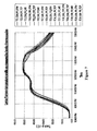
- Figure 7 shows exemplary furnace temperature profiles measured by in-situ thermal couples according to an embodiment of the present invention.
- Figure 8 shows exemplary temperature profile set points at various zones in a furnace according to an embodiment of the present invention.
- Figure 9 shows an exemplary furnace temperature profile and substrate temperature uniformity according to an embodiment of the present invention.
- Figure 10 shows an exemplary cell open-circuit voltage distribution from ten substrates in a furnace according to an embodiment of the present invention.
- the present invention relates generally to photovoltaic techniques. More particularly, the present invention provides a method and structure for a thin film photovoltaic device using a copper indium diselenide species (CIS), copper indium gallium diselenide species (CIGS), and/or others.
- CIS copper indium diselenide species
- CGS copper indium gallium diselenide species
- the invention can be applied to photovoltaic modules, flexible sheets, building or window glass, automotive, and others.
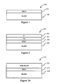
- FIG. 1 is a simplified diagram of a transparent substrate with an overlying electrode layer according to an embodiment of the present invention.
- structure 100 includes a transparent substrate 104.
- substrate 104 can be a glass substrate, for example, a soda lime glass.
- substrates include borosilicate glass, acrylic glass, sugar glass, specialty CorningTM glass, and others.
- a contact layer comprising a metal electrode layer 102 is deposited upon substrate 104.
- the metal electrode layer 102 comprises metal material that is characterized by a predetermined conductivity that is optimized for thin-film based solar cell applications.
- the metal electrode layer 102 may be deposited in various ways.
- the metal electrode layer 102 comprises primarily a film of molybdenum that is deposited by sputtering.
- the thickness may range form 200 to 700 nm.
- a sputtering apparatus such as a DC magnetron sputtering apparatus, can be used to deposit a thin film of materials upon a substrate.
- Such apparatus is well known and commercially available. But it is to be understood that other types of equipments and/or processes, such as evaporation in vacuum based environment may be used as well.
- the sputtering deposition process is described below.
- Sputter deposition is a physical vapor deposition (PVD) method of depositing thin films by sputtering, or ejecting, material from a "target", or source, which then deposits onto a substrate, such as a silicon wafer or glass.
- PVD physical vapor deposition
- Sputtered atoms ejected from the target have a wide energy distribution, typically up to 10's ofeV's (100000 K). The entire range from high-energy ballistic impact to low-energy thermalized motion is accessible by changing the background gas pressure.
- the sputtering gas is often an inert gas such as argon.
- the atomic weight of the sputtering gas should be close to the atomic weight of the target, so for sputtering light elements neon is preferable, while for heavy elements krypton or xenon are used.
- Reactive gases can also be used to sputter compounds.
- the compound can be formed on the target surface, in-flight or on the substrate depending on the process parameters. The availability of many parameters that control sputter deposition make it a complex process, but also allow experts a large degree of control over the growth and microstructure of the film.
- FIG. 2 is a simplified diagram of a composite structure including copper and indium material according to an embodiment of the present invention.
- structure 200 is includes a glass substrate 208, preferably soda lime glass, which is about 1 to 3 millimeters thick.
- the glass substrate 208 serves as a supporting layer.
- the metal layer 206 is deposited upon substrate 208.
- the metal layer 206 serves as a metal electrode layer to provide electrical contact.
- the layer 206 comprises primarily a film of molybdenum which has been deposited by sputtering to a thickness of from 200 to 700 nm.
- an initial film of chromium is first deposited upon glass 208.
- the chromium is used to insure good adhesion of the overall structure to the substrate 208.
- Other types of material may also be used in a barrier layer, such as silicon dioxide, silicon nitride, etc.
- Layers 204 and 202 include primarily a copper layer and an indium layer deposited upon metal layer 206 by a sputtering process.
- the indium layer overlays the copper layer.
- the copper layer overlays the indium layer.
- a sputtering apparatus such as a DC magnetron sputtering apparatus, is used to deposit the thin film (e.g., layer 202, 204, and/or 206) of materials upon a substrate.
- the thin film e.g., layer 202, 204, and/or 206
- various types of sputtering apparatus may be used.
- Such apparatus is well known and commercially available.
- Other material can also be used.
- techniques described throughout the present application are flexible and that other types of equipments and/or processes, such as evaporation in vacuum based environment may be used as well for depositing copper and indium material.
- gallium material (not shown in Figure 2 ) may be formed deposited in addition to the copper and indium material.
- the ratio between the copper and indium+gallium material is less than 1 (e.g., Cu/III ⁇ 0.92 ⁇ 0.96, here III means group III); that is, less than one part of copper per one part of indium material.
- the structure 200 is formed by processing the structure 100.
- the Cu and In are deposited onto the structure 100 to form the structure 200.
- sputtering process is used for forming the copper and/or indium layer.
- the Cu film and the In film are shown as two separate layers.
- a Cu/In composite or Cu/In alloy is formed during the sputtering process, as shown in Figure 2A .
- gallium material (not shown in Figure 2 ) may be formed deposited in addition to the copper and indium material
- FIG. 2A is a simplified diagram of a composite structure 210 including a copper and indium composite film according to another embodiment of the present invention.
- the structure 210 includes a transparent substrate 216.
- substrate 216 can be a glass substrate, for example, a soda lime glass.
- a back contact comprises a metal electrode layer 214 is deposited upon substrate 216.
- the layer 214 comprises primarily a film of molybdenum material is deposited by sputtering.
- an initial film of chromium is deposited upon glass 216 before depositing the molybdenum material to provide for good adhesion of the overall structure to the substrate 210.
- the layer 212 comprises primarily a copper (and gallium) indium alloy or copper (gallium) indium composite material.
- a copper (or CuGa alloy) indium alloy material is formed from separate layers of copper (or CuGa alloy) material and indium material, which diffuse into each layer.
- the process of forming of copper indium (or CuInGa) alloy material is performed by subjecting the structure to a high temperature annealing in an environment containing gaseous selenium species.
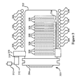
- FIG. 3 is a simplified diagram of a furnace according to an embodiment of the present invention.
- a furnace 300 includes a process chamber 302 and a chamber lid 304
- the reaction chamber 302 is characterized by avolume of more than 200 liters.
- typical volume for research related application is may be as low as a few liters, while the production furnace can increase a volume of over 2000 liters.
- the furnace 300 includes a vacuum-pumping machine that comprises a turbo molecular pump 310 and a rotary pump 312.
- the vacuum-pumping machine can be implemented by way of a combination of a mechanical booster pump and a dry pump.
- the raw material gas and/or a diluting gas such as helium, nitrogen, argon, or hydrogen can be introduced in process chamber 302 via a gas injection pipe 314, if demanded by the specific applications and/or processes.
- the chamber 302 is evacuated by the turbo molecular pump 310 via the rotary pump 312 that is connected with a manifold 316 via a gate valve and a conductance valve 318.
- a heating element 306 is mounted outside the reaction chamber 302.
- the chamber lid 304 of the chamber is built with embedded temperature control elements.
- the temperature control elements include lamps for generating heat and cooling water pipes for actual temperature control.
- the lid 304 also includes quartz baffles (not shown) that serves an element for controlling exchange of heat and mass (gases) between a main spatial region of the chamber 302 and a spatial region surrounding the lid 304.
- quartz baffles serves an element for controlling exchange of heat and mass (gases) between a main spatial region of the chamber 302 and a spatial region surrounding the lid 304.
- the furnace 300 can be used for many applications. According to an embodiment, the furnace 300 is used to apply thermal energy to various types of substrates and to introduce various types of gaseous species, among others.
- one or more glass plates or substrates are positioned vertically near the center of chamber 302. In an alternative embodiment, these substrates may be placed vertically and parallel, or diagonal, or perpendicular to the chamber lid 304. Under certain conditions, the substrates may be loaded in a horizontal configuration if proper support is in place for preventing the warping of the large glass plates during the thermal treatment. Of course, the exact configuration varies with chamber design and processes.
- substrates 308 can be similar to those described in Figures 2 and 2A (e.g., Cu/In layers or composite Cu/In layer overlying a metal contact layer on a substrate). These layers placed in the process chamber in the presence of a gas containing selenium, such as hydrogen selenide H 2 Se. After annealing the material for a given period of time, the copper, indium and selenium interdiffuse and react to form a high quality copper indium diselenide (CIS) film and/or CIGS film.
- a gas containing selenium such as hydrogen selenide H 2 Se.
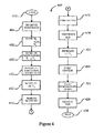
- FIG. 4 is a simplified diagram of a process for forming a copper indium diselenide layer according to an embodiment of the present invention.
- This diagram is merely an example, which should not limit the scope of the claims herein.
- One of ordinary skill in the art would recognize many other variations, modifications, and alternatives. It is also understood that the examples and embodiments described herein are for illustrative purposes only and that various modifications or changes in light thereof will be suggested to persons skilled in the art and are to be included within the spirit and purview of this process and scope of the appended claims.
- the method 400 begins at start, step 402.
- the user of the method begins at a process chamber, such as the one noted above, as well as others.
- the process chamber can be maintained at about room temperature before proceeding with the present method.
- a plurality of substrates is transferred into the process chamber, step 402.
- Each of the plurality of substrates can be provided in a vertical orientation with respect to gravity.
- the plurality of substrates can be defined by a number N, where N is greater than 5.
- the plurality of substrates can comprise 5 or more individual substrates.
- the plurality of substrates can comprise 40 or more individual substrates.
- each substrate can have a dimension of 65 cm to 165 cm or smaller. But it is understood that other dimensions are possible.
- Each of the substrates is maintained in substantially a planar configuration free from warp or damage. For example, if the substrates were provided in an orientation other than vertical with respect to gravity, the gravitational force could cause the substrates to sag and warp.
- glass substrates particular soda lime glass substrates, begin to soften at 480 °C.
- the substrates are also separate from one another according to a predetermined spacing to ensure even heating and reactions with gaseous species that are to be introduced to the furnace.
- gaseous species including a selenide species, and/or a carrier gas
- the gaseous species includes at least H 2 Se and nitrogen.
- the gaseous species other types of chemically inert gas, such as helium, argon, etc.
- the substrates are placed in the presence of a gas containing selenium, such as H 2 Se.
- the gaseous species may be introduced after a period of time so that the substrate has been heated to a predetermined temperature in an inert atmosphere (e.g., with nitrogen or argon filled at least 70% of furnace volume).
- step 408 The furnace is then heated up to a second temperature ranging from about 350 °C to 450 °C in step 408.
- the transfer of thermal energy for the purpose of heating the process chamber can be done by heating elements, heating coils, and the like.
- step 408 at least starts the formation of a copper indium diselenide film by reactions between the gaseous species and the copper and indium composite (or layered) structure on each of the substrates.
- separate layers of copper and indium material are diffused into each other to corm a single layer of copper indium alloy material.
- the second temperature is maintained for about 10 to 90 minutes at the heat treatment interval between 350 °C and 450 °C, step 410.
- the second temperature range can be from 390 °C to 410 °C.
- the period of time for maintaining the temperature at step 410 is provided to allow formation of the CIS and/or CIGS film material.
- the pressure inside the furnace may increase as well.
- a pressure release valve is used to keep the pressure within the furnace at approximately 650 torr.
- an additional carrier gas is selectively introduced into the furnace.
- the carrier case functions as a filling gas to keep the total amount of gas in the furnace constant and also helps maintain a substantially uniform temperature profile within the process chamber, step 410.
- the additional carrier gas can comprise of nitrogen gas N 2 .
- other types of chemically inert gas may be used as the additional carrier gas, such as helium, argon, carbon dioxide, among others.
- the additional carrier gas can be used to cool the furnace while maintaining a uniform temperature profile within the process chamber.
- the temperature distribution within a process chamber in a vacuum has variations and is unpredictable.
- an additional carrier gas such as nitrogen gas
- the temperature profile of within the process chamber can be stabilized without substantially altering the reaction chemistry.
- the nitrogen gas is introduced at a predetermined concentration level.
- the concentration level of nitrogen gas is dependent on the concentration level of other gas.
- various types of devices may be used in conjunction with or as a part of the furnace for the purpose of transferring the carrier gas into the furnace, in which the concentration, rate of transfer, time of injection, and/or other parameters can be controlled to ensure optimum results.
- step 412 As the temperature is maintained at the second temperature (step 410) or at least when the temperature above certain threshold, the removal of the residual selenide species begins, in step 412.
- a vacuum is formed in the process chamber through a vacuum pump, in step 414.
- a sulfide species is introduced, in step 416, while the furnace temperature is held constant for a predetermined period of time to allow the substrate reaches its desired temperature.
- the residual selenide removal process may continue until the process chamber is in vacuum configuration.
- a second temperature ramp up process is initiated, step 418.
- an optional step may include waiting before the temperature is ramped up to allow the temperature uniformity to improve for all substrates in the main spatial region of the chamber.
- the sulfide species is introduced with nitrogen.
- the nitrogen gas acts as a carrier gas occupying approximately 70 to 75% of the furnace.
- the temperature of the substrates needs to be increased.
- the temperature uniformity of the substrates is allowed to stabilize before the reaction with sulfur species takes place.
- the stabilized temperature of the substrates allow for better uniformity thin film overlaying the substrates as well as the structure integrity of the substrates themselves.
- the temperature of the furnace at this point is only allowed to increase if one or more preconditions are met.
- the precondition includes that the temperature difference of different regions of a substrate can be as small as about 20 °C.
- a specific calibrated stabilization period is used.
- the temperature of the furnace is increased to a third temperature ranging from about 500 °C to 525 °C.
- the third temperature is calibrated for reaction between the hydrogen sulfide species and the substrates in furnace.
- step 420 temperature is maintained at the third temperature for a period of time until the formation of the copper indium diselenide CIS (or CIGS if gallium is included) layer is completed.
- the step is set up for the purpose of extracting out one or more selenium species from the copper indium diselenide film in the ambient of the furnace comprising the sulfur species. It is to be appreciated that a predetermined amount of selenium are removed. In a specific embodiment, approximately 5% of the selenium is removed from the CIS film and is replaced by about 5% of sulfur. According to an embodiment, a complete reaction between the selenium with the CIS film is desired. After the removal of residual selenium, a controlled temperature ramp down process is initiated, in step 422.
- the furnace is cooled to the first temperature of about room temperature, and the remaining gaseous species are removed from the furnace, in step 424.
- the gaseous species are removed by a vacuum pumping machine.
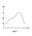
- the temperature sequence described above can be illustrated in the temperature profile in Figure 5 .
- step 420 additional steps may be performed depending on the desired end product. For example, if a CIS or CIGS type of thin-film solar cell is desired, additional processes are provided to provide additional structures, such as a transparent layer of material such as ZnO overlaying the CIS layer.
- the introduction of an additional carrier gas, step 410 can be conducted during any of the steps previously mentioned and any other process.
- other processes may include process involving the change of temperature, introduction and removal of gaseous species, change in flow rate of gaseous species, change in pressure of the process chamber, or the manipulation of any other parameter.
- steps are merely examples and should not limit the scope of the claims herein.
- One of ordinary skill in the art would recognize many other variations, modifications, and alternatives. For example, various steps outlined above may be added, removed, modified, rearranged, repeated, and/or overlapped, as contemplated within the scope of the invention.
- FIG. 5 is a simplified diagram of a temperature profile of the furnace according to an embodiment of the present invention. This diagram is merely an example, which should not limit the scope of the claims herein.
- the temperature profile further details the temperature ramping process in the above-described method outline ( Figure 4 ) and specification.
- An optimized temperature profile ( Figure 5 ) is provided to illustrate a heating process according to an embodiment of the present invention.
- the optimized profile regulates the process chamber in order to prevent the warping of large substrates at high temperatures. If the temperature is ramped up too high too quickly, warping or damage may occur due to the softening of glass.
- the total amount of thermal energy is determined in consideration of total thermal budget available to the substrates and to maintain the uniformity and structure integrity of the glass substrate.
- the substrate stays at a level of stabilization and relaxing in which the requisite structure integrity is maintained.
- material such as glass tends to deform at a temperature of 480 °C or higher, and thus caution is exercised to avoid prolong exposure of substrate at high temperatures.
- a plurality of substrates is put into the furnace.
- the plurality of substrates is provided in a vertical orientation with respect to a direction of gravity, with the plurality of substrates being defined by a number N, where N is greater than 5. In certain implementation, the number N is greater than 40.
- the substrates include glass substrates, such as soda lime glass.
- the furnace starts the process with a first temperature of about 30 °C (i.e., around room temperature). The furnace of course can start with a higher temperature, such as 100 °C. The furnace is then heated up to a second temperature ranging from about 350 °C to 450 °C.
- the second temperature is maintained for 10 to 60 minutes at the heat treatment interval between 350 °C to 450 °C.
- the size of glass substrate can be 20 cm x 20 cm up to 65 cm x 165 cm.
- a challenge in processing large substrate is the warping of the substrate at high temperatures.
- the temperature of the substrates needs to increases.
- the temperature uniformity of the substrates is allowed to stabilize before the reaction with sulfur species takes place.
- the stabilized temperature of the substrates allow for better uniformity thin film overlaying the substrates as well as the structure integrity of the substrates themselves.
- the temperature of the furnace at this point is only allowed to increase if one or more preconditions are met.
- the precondition includes that the temperature difference of different regions of a substrate is as small as about 20 °C.
- a specific calibrated stabilization period is used.
- the temperature of the furnace is increased to a third temperature ranging from about 500 °C to 525°C.
- the third temperature is calibrated for reaction between the sulfide species and the substrates in furnace. If the temperature is ramped up directly to T3, warping or damage may occur. As shown, the slope of ramping up from T2 to T3 is calibrated to reduce and/or eliminate the risk of damaging the substrate.
- the substrate can relax and stabilize. The maintaining time at this interval is set up according to the purpose of at least initiating formation of the copper indium diselenide film from the copper and indium composite structure on each of the substrates.
- the ambient of the furnace is changed such that the selenide species is removed and a sulfide species is introduced.
- a second temperature ramp up process is initiated.
- the temperature of the furnace is increased to a third temperature ranging from about 500 °C to 525 °C.
- the temperature of the furnace is maintained for 10 to 60 minutes at the heat treatment interval between 500 °C and 525 °C.
- the time interval with the temperature in a plateau in an ambient comprising a sulfur species, e.g., hydrogen sulfide gas, is set up for the purpose of extracting out one or more selenium species from the copper indium diselenide film.
- the residual selenide species can be thermally cranked or decomposed to elemental selenium particles, which can be carried away by a convective current from relative hot main spatial region of the chamber to a relative cold region such as the chamber lid.
- an exchange reaction occurs to replace sulfur species for the selenium species in the film overlying the substrate.
- a predetermined amount e.g., 5 to 10%
- selenium can be extracted to provide a proper amount of selenium concentration within the CIS film.
- a controlled temperature ramp-down process is initiated, as the furnace is then cooled to the first temperature of about room temperature.
- the cooling process is specifically calibrated. As a result of this process, the copper, indium, and selenium interdiffuse and react to form a high quality copper indium diselenide film.
- FIG. 5A is a simplified diagram of a temperature profile of the furnace according to an embodiment of the present invention. This diagram is merely an example, which should not limit the scope of the claims herein.
- the temperature profile further details the temperature ramping process in the above-described method outline ( Figure 4 ) and specification.
- An optimized temperature profile ( Figure 5A ) is provided to illustrate a heating process according to an embodiment of the present invention.
- T1 is approximately at room temperature. At this temperature, substrates are loaded into a furnace. Air is pumped out (e.g., by vacuum device) from the furnace, and H 2 Se and N 2 gas species are introduced into the furnace. For example, these gas species are introduced to the furnace so that at pressure of approximate 650 torr is reached.
- the rate of temperature ramping up is optimized to allow the relative uniform reaction between selenium and copper and indium (and possibly with addition of gallium).
- the T2 temperature is approximately between 350 °C and 450 °C.
- the furnace stays at the T2 temperature for about 10 to 60 minutes.
- the time staying at the T2 temperature is to allow for reaction between selenium and copper indium material.
- separate layers of copper and indium material form copper indium alloy while reacting with selenium material.
- CIS and/or CIGS material is formed at T2.
- the pressure inside the furnace is controlled to sustain a relative uniform pressure level of approximate 650 torr.
- a gas escape valve is used to release gases when the furnace heat up, where pressure increases due to gas expansion at high temperature.
- a sulfide gas along with inert gases (e.g., nitrogen, argon, helium, etc.) is introduced to the furnace, and the temperature inside the furnace increases from T2 to T3.
- inert gases e.g., nitrogen, argon, helium, etc.
- the temperature uniformity of the substrates is allowed to stabilize before the reaction with sulfur species takes place.
- the stabilized temperature of the substrates allow for better uniformity thin film overlaying the substrates as well as the structure integrity of the substrates themselves.
- the temperature of the furnace at this point is only allowed to increase if one or more preconditions are met.
- the precondition includes that the temperature difference of different regions of a substrate is as small as about 20 °C.
- a specific calibrated stabilization period is used.
- the temperature of the furnace is increased to a third temperature ranging from about 500 to 525°C.
- the third temperature is calibrated for reaction between the hydrogen sulfide species and the substrates in furnace.
- T3 is approximately 500 to 550 degrees Celsius.
- the temperature stays at T3 to allow the sulfide gas to interact with the CIGS and/or CIS material.
- the sulfur replaces approximately 3 to 10% of the selenium from the CIGS and/or CIS material.
- the furnace is cools down in the ambient of sulfide gas which is removed at last.
- Figure 7 shows exemplary furnace temperature profiles measured by in-situ thermal couples according to an embodiment of the present invention.
- This diagram is merely an example, which should not limit the scope of the claims herein.
- a large furnace is chosen to be the process chamber where a plurality of substrates has been loaded.
- temperature sensors are pre-installed for monitoring all substrates on bottom, middle, and top regions.
- Figure 7 shows the measured temperature profile during an actual processing run. It schematically illustrates realization of the temperature profile preset in Figure 5 or Figure 5A .
- FIG. 7 shows exemplary furnace temperature profiles measured by in-situ thermal couples according to an embodiment of the present invention.
- the furnace temperature profile is controlled by adjusting the heaters surrounding the process chamber. Additionally, depending on the internal structural design and substrate configuration when loaded in the substrate holder or boat, the temperature distribution may not be uniform. In fact, several temperature zones can be identified through experiment. Therefore, the temperature profile set point for corresponding zones can be separately controlled in order to achieve an actual temperature profile with improved uniformity.
- Figure 8 just shows exemplary temperature profile set points at various zones in a furnace according to an embodiment of the present invention.
- identifying various temperature zones in the furnace for setting independent temperature control is one method.
- Other methods of improving temperature uniformity include designing proper internal structural arrangement and substrate loading configuration. For example, adding certain baffles inside furnace's inner surface can partially isolate main processing zone for achieving better temperature uniformity and controlling the internal convective flow. Adding temperature control elements to an end cap (or lid) so that it can act as a "cryopump" inside the process chamber for reducing contamination and enhancing chemistry control of the reactive annealing of the film on substrate.
- Figure 9 shows exemplary furnace temperature profile and substrate temperature uniformity according to an embodiment of the present invention.
- FIG. 6A is a simplified diagram of a thin film copper indium diselenide device according to an embodiment of the present invention.
- structure 600 is supported on a glass substrate 610.
- the glass substrate comprises soda lime glass, which is about 1 to 3 millimeters thick.
- a back contact including a metal layer 608 is deposited upon substrate 610.
- layer 608 comprises primarily a film of molybdenum which has been deposited by sputtering.
- the first active region of the structure 600 comprises a semiconductor layer 606.
- the semiconductor layer includes p-type copper indium diselenide (CIS) material.
- CIS copper indium diselenide
- the second active portion of the structure 600 comprises layers 604 and 602 ofn-type semiconductor material, such as CdS or ZnO.
- Figure 6A shows the second active portion of the structure 600 comprising two CdS layers 602 and 604 with different levels of resistivity.
- Figure 6B shows the second active portion of the structure comprises both a CdS layer and a ZnO layer.
- FIG. 6B is a simplified diagram of a thin film copper indium diselenide device according to another embodiment of the present invention.
- structure 620 is supported on a glass substrate 630.
- the glass substrate comprises soda lime glass, which is about 1 to 3 millimeters thick.
- a back contact including a metal layer 628 is deposited upon substrate 630.
- layer 628 comprises primarily a film of molybdenum which has been deposited by sputtering.
- the first active region of the structure 620 comprises a semiconductor layer 626.
- the semiconductor layer includes p-type copper indium diselenide (CIS) material. It is to be understood that other the semiconductor layer may include other types of material, such as CIGS.
- the second active portion of the structure 620 comprises layers CdS 624 and ZnO 622 of n-type semiconductor material.
- a photovoltaic cell, or solar cell, such as device 600 described above, is configured as a large-area p-n junction.
- the photons may be reflected, pass through the transparent electrode layer, or become absorbed.
- the semiconductor layer absorbs the energy causing electron-hole pairs to be created.
- a photon needs to have greater energy than that of the band gap in order to excite an electron from the valence band into the conduction band. This allows the electrons to flow through the material to produce a current.
- the complementary positive charges, or holes flow in the direction opposite of the electrons in a photovoltaic cell.
- a solar panel having many photovoltaic cells can convert solar energy into direct current electricity.
- CIS copper indium diselenide
- the present invention provides methods for making CIS-based and/or CIGS-based solar cells on a large glass substrate for a solar panel.
- the devices structure described in Figures 6A and/or 6B can be patterned into individual solar cells on the glass substrate and interconnected to form the solar panel.
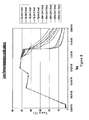
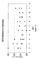
- FIG 10 shows an exemplary cell open-circuit voltage distribution from ten substrates in a furnace according to an embodiment of the present invention.
- This diagram is merely an example, which should not limit the scope of the claims herein.
- ten soda lime glass substrates have been loaded into a furnace described above and been carried out a series of large scale selenization and sufurization processes for forming a CIS based photovoltaic absorber film.
- a key parameter, cell open-circuit voltages Voc is measured around 0.5 V for cells made from those films out of the 10 substrates.
- Figure 10 just shows that the Voc value distribution has achieved desired uniformity across all substrates in this large scale production process.
Landscapes
- Chemical & Material Sciences (AREA)
- Chemical Kinetics & Catalysis (AREA)
- Engineering & Computer Science (AREA)
- Materials Engineering (AREA)
- Mechanical Engineering (AREA)
- Metallurgy (AREA)
- Organic Chemistry (AREA)
- Photovoltaic Devices (AREA)
Applications Claiming Priority (1)
| Application Number | Priority Date | Filing Date | Title |
|---|---|---|---|
| US12/568,644 US8008198B1 (en) | 2008-09-30 | 2009-09-28 | Large scale method and furnace system for selenization of thin film photovoltaic materials |
Publications (2)
| Publication Number | Publication Date |
|---|---|
| EP2302702A2 true EP2302702A2 (fr) | 2011-03-30 |
| EP2302702A3 EP2302702A3 (fr) | 2014-08-06 |
Family
ID=43480903
Family Applications (1)
| Application Number | Title | Priority Date | Filing Date |
|---|---|---|---|
| EP10181084.4A Withdrawn EP2302702A3 (fr) | 2009-09-28 | 2010-09-28 | Procédé à grande échelle et système de four pour la sélénisation de matériaux photovoltaïques à couche mince |
Country Status (4)
| Country | Link |
|---|---|
| US (1) | US8008198B1 (fr) |
| EP (1) | EP2302702A3 (fr) |
| CN (1) | CN102031497B (fr) |
| TW (1) | TWI521729B (fr) |
Families Citing this family (6)
| Publication number | Priority date | Publication date | Assignee | Title |
|---|---|---|---|---|
| KR20110097908A (ko) * | 2008-11-28 | 2011-08-31 | 볼커 프로브스트 | 반도체 층 또는 원소 셀레늄 및/또는 황으로 처리된 코팅 기판, 특히 평면 기판의 제조 방법 |
| TWI456779B (zh) * | 2011-12-28 | 2014-10-11 | 財團法人工業技術研究院 | 光吸收層之改質方法 |
| US8728855B2 (en) * | 2012-09-28 | 2014-05-20 | First Solar, Inc. | Method of processing a semiconductor assembly |
| FR3005371B1 (fr) * | 2013-05-03 | 2015-05-29 | Nexcis | Formation d'une couche semi-conductrice i-iii-vi2 par traitement thermique et chalcogenisation d'un precurseur metallique i-iii |
| CN109273355B (zh) * | 2018-06-06 | 2022-03-01 | 鹤壁维达科巽电气有限公司 | 一种硒整流片制备工艺 |
| CN115699258B (zh) * | 2020-06-04 | 2025-07-08 | 胜高股份有限公司 | 使用卧式热处理炉的硅晶圆的热处理方法 |
Citations (2)
| Publication number | Priority date | Publication date | Assignee | Title |
|---|---|---|---|---|
| US4611091A (en) | 1984-12-06 | 1986-09-09 | Atlantic Richfield Company | CuInSe2 thin film solar cell with thin CdS and transparent window layer |
| US4612411A (en) | 1985-06-04 | 1986-09-16 | Atlantic Richfield Company | Thin film solar cell with ZnO window layer |
Family Cites Families (20)
| Publication number | Priority date | Publication date | Assignee | Title |
|---|---|---|---|---|
| US4915745A (en) * | 1988-09-22 | 1990-04-10 | Atlantic Richfield Company | Thin film solar cell and method of making |
| US4996108A (en) | 1989-01-17 | 1991-02-26 | Simon Fraser University | Sheets of transition metal dichalcogenides |
| DK170189B1 (da) | 1990-05-30 | 1995-06-06 | Yakov Safir | Fremgangsmåde til fremstilling af halvlederkomponenter, samt solcelle fremstillet deraf |
| EP0460287A1 (fr) | 1990-05-31 | 1991-12-11 | Siemens Aktiengesellschaft | Nouvelle cellule solaire en chalcopyrite |
| US5261968A (en) | 1992-01-13 | 1993-11-16 | Photon Energy, Inc. | Photovoltaic cell and method |
| US5501744A (en) | 1992-01-13 | 1996-03-26 | Photon Energy, Inc. | Photovoltaic cell having a p-type polycrystalline layer with large crystals |
| US5248349A (en) | 1992-05-12 | 1993-09-28 | Solar Cells, Inc. | Process for making photovoltaic devices and resultant product |
| US6328871B1 (en) | 1999-08-16 | 2001-12-11 | Applied Materials, Inc. | Barrier layer for electroplating processes |
| JPWO2004090995A1 (ja) | 2003-04-09 | 2006-07-06 | 松下電器産業株式会社 | 太陽電池 |
| EP1521308A1 (fr) | 2003-10-02 | 2005-04-06 | Scheuten Glasgroep | Composant semiconducteur sphérique ou granulaire utilisé pour des cellules solaires et son procédé de fabrication; procédé de fabrication d'une cellule solaire avec ce composant semiconducteur et cellule solaire |
| US20070169810A1 (en) | 2004-02-19 | 2007-07-26 | Nanosolar, Inc. | High-throughput printing of semiconductor precursor layer by use of chalcogen-containing vapor |
| EP2469605A3 (fr) | 2004-02-20 | 2014-03-05 | Sharp Kabushiki Kaisha | Substrat pour dispositif de conversion photoélectrique, dispositif de conversion photoélectrique et dispositif de conversion photoélectrique empilé |
| CN100463230C (zh) * | 2004-05-11 | 2009-02-18 | 本田技研工业株式会社 | 黄铜矿型薄膜太阳能电池的制造方法 |
| JP4131965B2 (ja) * | 2004-12-28 | 2008-08-13 | 昭和シェル石油株式会社 | Cis系薄膜太陽電池の光吸収層の作製方法 |
| CN100413097C (zh) * | 2005-06-03 | 2008-08-20 | 清华大学 | 铜铟镓硒或铜铟镓硫或铜铟镓硒硫薄膜太阳能电池吸收层的制备方法 |
| US8017860B2 (en) | 2006-05-15 | 2011-09-13 | Stion Corporation | Method and structure for thin film photovoltaic materials using bulk semiconductor materials |
| TW200810167A (en) | 2006-08-09 | 2008-02-16 | Ind Tech Res Inst | Dye-sensitized solar cell and the method of fabricating thereof |
| US8426722B2 (en) | 2006-10-24 | 2013-04-23 | Zetta Research and Development LLC—AQT Series | Semiconductor grain and oxide layer for photovoltaic cells |
| JP4620105B2 (ja) * | 2007-11-30 | 2011-01-26 | 昭和シェル石油株式会社 | Cis系薄膜太陽電池の光吸収層の製造方法 |
| CN101475315B (zh) * | 2009-02-03 | 2011-08-17 | 泉州创辉光伏太阳能有限公司 | 黄铜矿类铜铟镓的硒化物或硫化物半导体薄膜材料的制备方法 |
-
2009
- 2009-09-28 US US12/568,644 patent/US8008198B1/en not_active Expired - Fee Related
-
2010
- 2010-09-28 CN CN201010503974.3A patent/CN102031497B/zh not_active Expired - Fee Related
- 2010-09-28 TW TW099132908A patent/TWI521729B/zh not_active IP Right Cessation
- 2010-09-28 EP EP10181084.4A patent/EP2302702A3/fr not_active Withdrawn
Patent Citations (2)
| Publication number | Priority date | Publication date | Assignee | Title |
|---|---|---|---|---|
| US4611091A (en) | 1984-12-06 | 1986-09-09 | Atlantic Richfield Company | CuInSe2 thin film solar cell with thin CdS and transparent window layer |
| US4612411A (en) | 1985-06-04 | 1986-09-16 | Atlantic Richfield Company | Thin film solar cell with ZnO window layer |
Also Published As
| Publication number | Publication date |
|---|---|
| US20110229989A1 (en) | 2011-09-22 |
| EP2302702A3 (fr) | 2014-08-06 |
| US8008198B1 (en) | 2011-08-30 |
| CN102031497A (zh) | 2011-04-27 |
| TWI521729B (zh) | 2016-02-11 |
| CN102031497B (zh) | 2014-12-10 |
| TW201123519A (en) | 2011-07-01 |
Similar Documents
| Publication | Publication Date | Title |
|---|---|---|
| US7910399B1 (en) | Thermal management and method for large scale processing of CIS and/or CIGS based thin films overlying glass substrates | |
| US8377736B2 (en) | System and method for transferring substrates in large scale processing of CIGS and/or CIS devices | |
| US8053274B2 (en) | Self cleaning large scale method and furnace system for selenization of thin film photovoltaic materials | |
| EP2319954A1 (fr) | Procédé pour la fabrication d'une couche mince de CIS et/ou de CIGS sur des substrats de verre | |
| JP2014513413A (ja) | 五元化合物半導体CZTSSeおよび薄膜太陽電池の製造方法 | |
| US8008198B1 (en) | Large scale method and furnace system for selenization of thin film photovoltaic materials | |
| KR101299189B1 (ko) | 멀티 스테이지공정을 이용한 대면적 유리기판 cigs 박막의 연속 제조용 인라인 장비시스템과 대면적 유리기판 cigs 박막의 제조방법 | |
| JP2012142342A (ja) | 成膜装置および光電変換素子の製造方法 | |
| US8372684B1 (en) | Method and system for selenization in fabricating CIGS/CIS solar cells | |
| Schulte et al. | Toward efficient Cu (In, Ga) Se2 solar cells prepared by reactive magnetron co‐sputtering from metallic targets in an Ar: H2Se atmosphere | |
| CN102034896B (zh) | 利用自清洁熔炉制造铜铟二硒化物半导体膜的方法 | |
| WO2011135420A1 (fr) | Procédé destiné à la production d'une couche de semi-conducteur composite |
Legal Events
| Date | Code | Title | Description |
|---|---|---|---|
| PUAI | Public reference made under article 153(3) epc to a published international application that has entered the european phase |
Free format text: ORIGINAL CODE: 0009012 |
|
| AK | Designated contracting states |
Kind code of ref document: A2 Designated state(s): AL AT BE BG CH CY CZ DE DK EE ES FI FR GB GR HR HU IE IS IT LI LT LU LV MC MK MT NL NO PL PT RO SE SI SK SM TR |
|
| AX | Request for extension of the european patent |
Extension state: BA ME RS |
|
| PUAL | Search report despatched |
Free format text: ORIGINAL CODE: 0009013 |
|
| AK | Designated contracting states |
Kind code of ref document: A3 Designated state(s): AL AT BE BG CH CY CZ DE DK EE ES FI FR GB GR HR HU IE IS IT LI LT LU LV MC MK MT NL NO PL PT RO SE SI SK SM TR |
|
| AX | Request for extension of the european patent |
Extension state: BA ME RS |
|
| RIC1 | Information provided on ipc code assigned before grant |
Ipc: H01L 31/18 20060101AFI20140702BHEP |
|
| 17P | Request for examination filed |
Effective date: 20150206 |
|
| RBV | Designated contracting states (corrected) |
Designated state(s): AL AT BE BG CH CY CZ DE DK EE ES FI FR GB GR HR HU IE IS IT LI LT LU LV MC MK MT NL NO PL PT RO SE SI SK SM TR |
|
| STAA | Information on the status of an ep patent application or granted ep patent |
Free format text: STATUS: THE APPLICATION IS DEEMED TO BE WITHDRAWN |
|
| 18D | Application deemed to be withdrawn |
Effective date: 20170401 |